EP3799019B1 - Anzeigevorrichtung - Google Patents
Anzeigevorrichtung Download PDFInfo
- Publication number
- EP3799019B1 EP3799019B1 EP20196142.2A EP20196142A EP3799019B1 EP 3799019 B1 EP3799019 B1 EP 3799019B1 EP 20196142 A EP20196142 A EP 20196142A EP 3799019 B1 EP3799019 B1 EP 3799019B1
- Authority
- EP
- European Patent Office
- Prior art keywords
- flicker
- driving
- display panel
- determiner
- driving frequency
- Prior art date
- Legal status (The legal status is an assumption and is not a legal conclusion. Google has not performed a legal analysis and makes no representation as to the accuracy of the status listed.)
- Active
Links
Images




Classifications
-
- G—PHYSICS
- G09—EDUCATION; CRYPTOGRAPHY; DISPLAY; ADVERTISING; SEALS
- G09G—ARRANGEMENTS OR CIRCUITS FOR CONTROL OF INDICATING DEVICES USING STATIC MEANS TO PRESENT VARIABLE INFORMATION
- G09G3/00—Control arrangements or circuits, of interest only in connection with visual indicators other than cathode-ray tubes
- G09G3/20—Control arrangements or circuits, of interest only in connection with visual indicators other than cathode-ray tubes for presentation of an assembly of a number of characters, e.g. a page, by composing the assembly by combination of individual elements arranged in a matrix no fixed position being assigned to or needed to be assigned to the individual characters or partial characters
-
- G—PHYSICS
- G09—EDUCATION; CRYPTOGRAPHY; DISPLAY; ADVERTISING; SEALS
- G09G—ARRANGEMENTS OR CIRCUITS FOR CONTROL OF INDICATING DEVICES USING STATIC MEANS TO PRESENT VARIABLE INFORMATION
- G09G3/00—Control arrangements or circuits, of interest only in connection with visual indicators other than cathode-ray tubes
- G09G3/20—Control arrangements or circuits, of interest only in connection with visual indicators other than cathode-ray tubes for presentation of an assembly of a number of characters, e.g. a page, by composing the assembly by combination of individual elements arranged in a matrix no fixed position being assigned to or needed to be assigned to the individual characters or partial characters
- G09G3/2007—Display of intermediate tones
-
- G—PHYSICS
- G09—EDUCATION; CRYPTOGRAPHY; DISPLAY; ADVERTISING; SEALS
- G09G—ARRANGEMENTS OR CIRCUITS FOR CONTROL OF INDICATING DEVICES USING STATIC MEANS TO PRESENT VARIABLE INFORMATION
- G09G3/00—Control arrangements or circuits, of interest only in connection with visual indicators other than cathode-ray tubes
- G09G3/20—Control arrangements or circuits, of interest only in connection with visual indicators other than cathode-ray tubes for presentation of an assembly of a number of characters, e.g. a page, by composing the assembly by combination of individual elements arranged in a matrix no fixed position being assigned to or needed to be assigned to the individual characters or partial characters
- G09G3/2092—Details of a display terminals using a flat panel, the details relating to the control arrangement of the display terminal and to the interfaces thereto
-
- G—PHYSICS
- G09—EDUCATION; CRYPTOGRAPHY; DISPLAY; ADVERTISING; SEALS
- G09G—ARRANGEMENTS OR CIRCUITS FOR CONTROL OF INDICATING DEVICES USING STATIC MEANS TO PRESENT VARIABLE INFORMATION
- G09G2310/00—Command of the display device
- G09G2310/02—Addressing, scanning or driving the display screen or processing steps related thereto
- G09G2310/0264—Details of driving circuits
- G09G2310/027—Details of drivers for data electrodes, the drivers handling digital grey scale data, e.g. use of D/A converters
-
- G—PHYSICS
- G09—EDUCATION; CRYPTOGRAPHY; DISPLAY; ADVERTISING; SEALS
- G09G—ARRANGEMENTS OR CIRCUITS FOR CONTROL OF INDICATING DEVICES USING STATIC MEANS TO PRESENT VARIABLE INFORMATION
- G09G2310/00—Command of the display device
- G09G2310/08—Details of timing specific for flat panels, other than clock recovery
-
- G—PHYSICS
- G09—EDUCATION; CRYPTOGRAPHY; DISPLAY; ADVERTISING; SEALS
- G09G—ARRANGEMENTS OR CIRCUITS FOR CONTROL OF INDICATING DEVICES USING STATIC MEANS TO PRESENT VARIABLE INFORMATION
- G09G2320/00—Control of display operating conditions
- G09G2320/02—Improving the quality of display appearance
- G09G2320/0247—Flicker reduction other than flicker reduction circuits used for single beam cathode-ray tubes
-
- G—PHYSICS
- G09—EDUCATION; CRYPTOGRAPHY; DISPLAY; ADVERTISING; SEALS
- G09G—ARRANGEMENTS OR CIRCUITS FOR CONTROL OF INDICATING DEVICES USING STATIC MEANS TO PRESENT VARIABLE INFORMATION
- G09G2320/00—Control of display operating conditions
- G09G2320/06—Adjustment of display parameters
- G09G2320/0606—Manual adjustment
-
- G—PHYSICS
- G09—EDUCATION; CRYPTOGRAPHY; DISPLAY; ADVERTISING; SEALS
- G09G—ARRANGEMENTS OR CIRCUITS FOR CONTROL OF INDICATING DEVICES USING STATIC MEANS TO PRESENT VARIABLE INFORMATION
- G09G2320/00—Control of display operating conditions
- G09G2320/08—Arrangements within a display terminal for setting, manually or automatically, display parameters of the display terminal
-
- G—PHYSICS
- G09—EDUCATION; CRYPTOGRAPHY; DISPLAY; ADVERTISING; SEALS
- G09G—ARRANGEMENTS OR CIRCUITS FOR CONTROL OF INDICATING DEVICES USING STATIC MEANS TO PRESENT VARIABLE INFORMATION
- G09G2320/00—Control of display operating conditions
- G09G2320/10—Special adaptations of display systems for operation with variable images
-
- G—PHYSICS
- G09—EDUCATION; CRYPTOGRAPHY; DISPLAY; ADVERTISING; SEALS
- G09G—ARRANGEMENTS OR CIRCUITS FOR CONTROL OF INDICATING DEVICES USING STATIC MEANS TO PRESENT VARIABLE INFORMATION
- G09G2330/00—Aspects of power supply; Aspects of display protection and defect management
- G09G2330/02—Details of power systems and of start or stop of display operation
- G09G2330/021—Power management, e.g. power saving
-
- G—PHYSICS
- G09—EDUCATION; CRYPTOGRAPHY; DISPLAY; ADVERTISING; SEALS
- G09G—ARRANGEMENTS OR CIRCUITS FOR CONTROL OF INDICATING DEVICES USING STATIC MEANS TO PRESENT VARIABLE INFORMATION
- G09G2340/00—Aspects of display data processing
- G09G2340/04—Changes in size, position or resolution of an image
-
- G—PHYSICS
- G09—EDUCATION; CRYPTOGRAPHY; DISPLAY; ADVERTISING; SEALS
- G09G—ARRANGEMENTS OR CIRCUITS FOR CONTROL OF INDICATING DEVICES USING STATIC MEANS TO PRESENT VARIABLE INFORMATION
- G09G2340/00—Aspects of display data processing
- G09G2340/04—Changes in size, position or resolution of an image
- G09G2340/0407—Resolution change, inclusive of the use of different resolutions for different screen areas
- G09G2340/0435—Change or adaptation of the frame rate of the video stream
-
- G—PHYSICS
- G09—EDUCATION; CRYPTOGRAPHY; DISPLAY; ADVERTISING; SEALS
- G09G—ARRANGEMENTS OR CIRCUITS FOR CONTROL OF INDICATING DEVICES USING STATIC MEANS TO PRESENT VARIABLE INFORMATION
- G09G2360/00—Aspects of the architecture of display systems
- G09G2360/14—Detecting light within display terminals, e.g. using a single or a plurality of photosensors
-
- G—PHYSICS
- G09—EDUCATION; CRYPTOGRAPHY; DISPLAY; ADVERTISING; SEALS
- G09G—ARRANGEMENTS OR CIRCUITS FOR CONTROL OF INDICATING DEVICES USING STATIC MEANS TO PRESENT VARIABLE INFORMATION
- G09G2360/00—Aspects of the architecture of display systems
- G09G2360/14—Detecting light within display terminals, e.g. using a single or a plurality of photosensors
- G09G2360/144—Detecting light within display terminals, e.g. using a single or a plurality of photosensors the light being ambient light
-
- G—PHYSICS
- G09—EDUCATION; CRYPTOGRAPHY; DISPLAY; ADVERTISING; SEALS
- G09G—ARRANGEMENTS OR CIRCUITS FOR CONTROL OF INDICATING DEVICES USING STATIC MEANS TO PRESENT VARIABLE INFORMATION
- G09G2360/00—Aspects of the architecture of display systems
- G09G2360/16—Calculation or use of calculated indices related to luminance levels in display data
Definitions
- Example embodiments of the present inventive concept relate to a display apparatus and examples useful for understanding the present invention relate a method of driving a display panel using the display apparatus. More particularly, example embodiments of the present inventive concept relate to a display apparatus reducing power consumption and enhancing a display quality and examples useful for understanding the present invention relate a method of driving a display panel using the display apparatus.
- US 2016/078815 A1 describes a device including an OLED pixel and a control circuit controlled at a refresh rate thereof, wherein the device includes first and second dummy control circuits having similar operating characteristics to the control circuit.
- a controller and logic circuit switch on the first and second dummy control circuits and apply an input voltage so the first and second dummy control circuits output first and second output voltages.
- US 2017/018234 A1 describes a display apparatus including a backlight to generate light, a display panel to display an image by utilizing the light, a driving part to provide image signals corresponding to the image to the display panel, and a timing controller to drive the backlight, to drive the driving part at a first frequency when the image is a moving image, and to drive the driving part at a second frequency lower than the first frequency when the image is a still image.
- the timing controller is to set the second frequency based on a value obtained by applying a reduction rate of a flicker index corresponding to a dimming index of the backlight to a flicker index of image signals of a previous frame.
- KR 2016/0053377 A describes a display device including a display panel, a driving unit, and a control unit.
- the display panel displays an image.
- the driving unit drives the display panel.
- the control unit varies a driving frequency of the driving unit in response to a change in brightness of the display panel.
- Recent research focus has been on minimizing power consumption of an electronic device, particularly a mobile device such as a tablet personal computer (PC) and a notebook PC.
- a mobile device such as a tablet personal computer (PC) and a notebook PC.
- the display panel may be driven at a low frequency mode so that power consumption of the display panel can be reduced.
- driving the display panel at a relatively low frequency mode may cause image flicker resulting in a poor display quality.
- image flickering may become a more serious issue at a portion (e.g., a lower portion) of the display panel that is farther from a data driver due to a voltage drop of a driving voltage or a data voltage over a data line.
- Examples useful for understanding the present inventive concept also relate to a method of driving a display panel using the display apparatus.
- the display apparatus includes a display panel, a data driver, and a driving controller.
- the display panel includes a data line and a pixel connected to the data line.
- the display panel is configured to display an image based on an input image data.
- the data driver is configured to output a data voltage to the data line.
- the driving controller is configured to control an operation of the data driver and to determine a driving frequency of the display panel based on the input image data.
- the driving controller includes a flicker value storage configured to store flicker values for grayscale values corresponding to the input image data, a voltage drop determiner configured to adjust a flicker value of the flicker values based on a voltage drop of the display panel, a still image determiner configured to determine whether the input image data is a still image or a video image, and a driving frequency determiner configured to determine the driving frequency of the display panel using the flicker value based on the input image data being the still image.
- a flicker value storage configured to store flicker values for grayscale values corresponding to the input image data
- a voltage drop determiner configured to adjust a flicker value of the flicker values based on a voltage drop of the display panel
- a still image determiner configured to determine whether the input image data is a still image or a video image
- a driving frequency determiner configured to determine the driving frequency of the display panel using the flicker value based on the input image data being the still image.
- the voltage drop determiner may be configured to determine a just-noticeable difference of a user according to the voltage drop of the display panel.
- the flicker value may be adjusted according to the just-noticeable difference.
- the flicker value storage may include a plurality of flicker lookup tables.
- the voltage drop determiner determines that a reference just-noticeable difference corresponds to a first just-noticeable difference according to the voltage drop of the display panel, and the driving frequency determiner may be configured to determine the driving frequency using a first flicker lookup table corresponding to the first just-noticeable difference.
- the voltage drop determiner determines that the reference just-noticeable difference corresponds to a second just-noticeable difference according to the voltage drop of the display panel, and the driving frequency determiner may be configured to determine the driving frequency using a second flicker lookup table corresponding to the second just-noticeable difference.
- the voltage drop determiner may be configured to set a reference just-noticeable difference based on the voltage drop.
- a size of a low driving grayscale range may be determined based on the just-noticeable difference.
- the voltage drop determiner may determine the voltage drop by sensing a current flowing through the pixel or a current flowing through the data line.
- the display apparatus may further include an ambient light determiner configured to adjust the flicker value based on an intensity of an ambient light.
- the ambient light determiner may be configured to determine a just-noticeable difference of a user according to the intensity of the ambient light.
- the flicker value may be adjusted according to the just-noticeable difference.
- the ambient light determiner may be configured to set a reference just-noticeable difference based on the intensity of the ambient light.
- a size of a low driving grayscale range may be determined based on the just-noticeable difference.
- the display apparatus may further include a user luminance setter configured to adjust the flicker value based on a user luminance setting value set by a user.
- the user luminance setter may be configured to determine a just-noticeable difference of the user according to the user luminance setting value.
- the flicker value may be adjusted according to the just-noticeable difference.
- the user luminance setter may be configured to set a reference just-noticeable difference based on the user luminance setting value.
- a size of a low driving grayscale range may be determined based on the just-noticeable difference.
- the driving controller may further include a fixed frequency determiner configured to determine a type of an input frequency of the input image data by counting a number of pulses of a horizontal synchronizing signal between a first pulse and a second pulse of a vertical synchronizing signal or by counting a number of pulses of a data enable signal between the first pulse and the second pulse of the vertical synchronizing signal.
- a fixed frequency determiner configured to determine a type of an input frequency of the input image data by counting a number of pulses of a horizontal synchronizing signal between a first pulse and a second pulse of a vertical synchronizing signal or by counting a number of pulses of a data enable signal between the first pulse and the second pulse of the vertical synchronizing signal.
- the fixed frequency determiner may be configured to generate a frequency flag indicating the type of the input frequency of the input image data.
- the driving frequency determiner may be configured to determine the driving frequency of the display panel based on the frequency flag.
- the display panel may include a plurality of segments.
- the driving controller may be configured to determine the driving frequency of the display panel based on the plurality of segments.
- the display apparatus may further include a driving mode setter configured to adjust the flicker value based on a luminance of a display image according to a driving mode.
- the driving mode setter may be configured to determine a just-noticeable difference of a user according to the driving mode.
- the flicker value may be adjusted according to the just-noticeable difference.
- the driving mode setter may be configured to set a reference just-noticeable difference based on the luminance of the display image according to the driving mode.
- a size of a low driving grayscale range may be determined based on the just-noticeable difference.
- the method includes determining whether an input image data is a still image or a video image, determining a driving frequency of the display panel using a flicker value storage that stores flicker values for grayscale values corresponding to the input image data based on the input image data being the still image, and outputting a data voltage to a data line of the display panel based on the driving frequency.
- the flicker value is adjusted based on a voltage drop of the display panel.
- the flicker value may be adjusted according to a just-noticeable difference of a user and the voltage drop of the display panel.
- the flicker value storage may include a plurality of flicker lookup tables.
- a reference just-noticeable difference is determined to correspond to a first just-noticeable difference according to the voltage drop of the display panel, and the driving frequency may be determined using a first flicker lookup table corresponding to the first just-noticeable difference.
- the reference just-noticeable difference is determined to correspond to a second just-noticeable difference according to the voltage drop of the display panel, and the driving frequency may be determined using a second flicker lookup table corresponding to the second just-noticeable difference.
- a reference just-noticeable difference may be set based on the voltage drop.
- a size of a low driving grayscale range may be determined based on the just-noticeable difference.
- the voltage drop may be determined by sensing a current flowing through the pixel or a current flowing through the data line.
- the flicker value may be adjusted based on an intensity of an ambient light or a user luminance setting value.
- the driving frequency is determined according to an image displayed on the display panel to reduce power consumption of the display apparatus.
- the driving frequency is determined using a flicker value of the image on the display panel to prevent a flicker of the image and enhance a display quality of the display panel.
- the display apparatus may include a voltage drop determiner for adjusting the flicker value based on the voltage drop of the display panel.
- FIG 1 is a block diagram illustrating a display apparatus according to an example embodiment of the present inventive concept.
- the display apparatus includes a display panel 100 and a display panel driver.
- the display panel driver includes a driving controller 200, a gate driver 300, a gamma reference voltage generator 400, and a data driver 500.
- the driving controller 200 and the data driver 500 may be integrally formed, and the driving controller 200, the gamma reference voltage generator 400, and the data driver 500 may be integrally formed.
- a driving module that integrally includes at least the driving controller 200 and the data driver 500 may be referred to as a timing controller embedded data driver (TED).
- the display panel 100 includes a plurality of gate lines GL, a plurality of data lines DL, and a plurality of pixels P connected to the gate lines GL and the data lines DL.
- the gate lines GL may extend in a first direction D1
- the data lines DL may extend in a second direction D2 crossing the first direction D1.
- the driving controller 200 may receive input image data IMG and an input control signal CONT from an external apparatus (not shown).
- the input image data IMG may include red image data, green image data, and blue image data.
- the input image data IMG may include white image data.
- the input image data IMG may include magenta image data, yellow image data, and cyan image data.
- the input control signal CONT may include a master clock signal and a data enable signal.
- the input control signal CONT may further include a vertical synchronizing signal and a horizontal synchronizing signal.
- the driving controller 200 generates a first control signal CONT1, a second control signal CONT2, a third control signal CONT3, and a data signal DATA based on the input image data IMG and the input control signal CONT.
- the driving controller 200 generates the first control signal CONT1 for controlling an operation of the gate driver 300 based on the input control signal CONT, and outputs the first control signal CONT1 to the gate driver 300.
- the first control signal CONT1 may include a vertical start signal and a gate clock signal.
- the driving controller 200 generates the second control signal CONT2 for controlling an operation of the data driver 500 based on the input control signal CONT, and outputs the second control signal CONT2 to the data driver 500.
- the second control signal CONT2 may include a horizontal start signal and a load signal.
- the driving controller 200 generates the data signal DATA based on the input image data IMG
- the driving controller 200 outputs the data signal DATA to the data driver 500.
- the driving controller 200 may adjust a driving frequency of the display panel 100 based on the input image data IMG
- the driving controller 200 generates the third control signal CONT3 for controlling an operation of the gamma reference voltage generator 400 based on the input control signal CONT, and outputs the third control signal CONT3 to the gamma reference voltage generator 400.
- FIGS. 2 to 6 A structure and an operation of the driving controller 200 are explained with reference to FIGS. 2 to 6 in further detail.
- the gate driver 300 generates gate signals in response to the first control signal CONT1 that is received from the driving controller 200.
- the gate driver 300 outputs the gate signals to the gate lines GL.
- the gate driver 300 may sequentially output the gate signals to the gate lines GL.
- the gate driver 300 may be mounted on the display panel 100or integrated on the display panel 100.
- the gamma reference voltage generator 400 generates a gamma reference voltage VGREF in response to the third control signal CONT3 that is received from the driving controller 200.
- the gamma reference voltage generator 400 provides the gamma reference voltage VGREF to the data driver 500.
- the gamma reference voltage VGREF may have a value corresponding to a level of the data signal DATA.
- the gamma reference voltage generator 400 may be disposed in the driving controller 200 or in the data driver 500.
- the data driver 500 receives the second control signal CONT2 and the data signal DATA from the driving controller 200 and receives the gamma reference voltage VGREF from the gamma reference voltage generator 400.
- the data driver 500 converts the data signal DATA into data voltages having an analog type using the gamma reference voltage VGREF.
- the data driver 500 outputs the data voltages to the data lines DL.
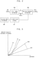
- FIG 2 is a block diagram of the driving controller 200 of FIG 1 according to an example embodiment of the present inventive concept.
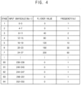
- FIG 3 is a graph illustrating a just-noticeable difference of a user.
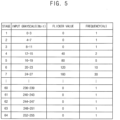
- FIG 4 is a table of an exemplary flicker value storage of FIG 2 .
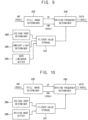
- FIG 5 is a table of an exemplary flicker value storage of FIG 2 .
- FIG 6 is a table of an exemplary flicker value storage of FIG 2 .
- the driving controller 200 includes a still image determiner 220, a driving frequency determiner 240, and a flicker value storage 260.
- the driving controller 200 further includes a voltage drop determiner 280.
- the still image determiner 220 determines whether the input image data IMG is a still image or a video image.
- the still image determiner 220 outputs a flag SF indicating whether the input image data IMG is the still image or the video image to the driving frequency determiner 240. For example, when the input image data IMG is the still image, the still image determiner 220 outputs the flag SF of 1 to the driving frequency determiner 240, and when the input image data IMG is the video image, the still image determiner 220 outputs the flag SF of 0 to the driving frequency determiner 240. If the display panel 100 operates in an always-on mode, the still image determiner 220 outputs the flag SF of 1 to the driving frequency determiner 240.
- the driving frequency determiner 240 drives the switching elements in the pixel in a low driving frequency mode.
- the driving frequency determiner 240 drives the switching elements in the pixel in a normal driving frequency mode.
- the driving frequency determiner 240 refers the flicker value storage 260 to determine the low driving frequency.
- the flicker value storage 260 includes a flicker value representing a degree of a flicker according to a grayscale value of the input image data IMG
- the flicker value storage 260 stores the grayscale value of the input image data IMG and the flicker value corresponding to the grayscale value of the input image data IMG
- the flicker value is used for determining the driving frequency of the display panel 100.
- the flicker value storage 260 includes a lookup table.
- the flicker value is set based on a just-noticeable difference of a user for the luminance.
- the just-noticeable difference represents a luminance difference which can be perceived by an average human.
- FIG 3 illustrates a curve CR of an absolute value of luminance difference of a red image, a curve CG of an absolute value of luminance difference of a green image, and a curve CB of an absolute value of luminance difference of a blue image.
- the just-noticeable difference is represented as a slope of the curve of an absolute value of luminance difference according to a luminance.
- the just-noticeable difference is determined to a first just-noticeable difference value JND1
- the flicker is not perceived to a user in an area under a line of the first just-noticeable difference value JND1 in FIG 3 .
- the flicker is not perceived to a user in an area under a line of the second just-noticeable difference value JND2 in FIG 3 .
- the just-noticeable difference is changed from the first just-noticeable difference value JND1 to the second just-noticeable difference value JND2
- the user gets more insensitive to the luminance difference.
- the just-noticeable difference is changed from the first just-noticeable difference value JND1 to the second just-noticeable difference value JND2
- the area where the user does not perceive the flicker increase, and a low driving grayscale range driven at the low driving frequency increased.
- the flicker value varies according to the just-noticeable difference.
- the voltage drop determiner 280 adjusts the flicker value based on a voltage drop of the display panel 100.
- the voltage drop includes a drop of a driving voltage of the pixel.
- the voltage drop includes a drop of the data voltage.
- the voltage drop determiner 280 determines the just-noticeable difference of the user according to the voltage drop of the display panel. In addition, the flicker value is adjusted according to the just-noticeable difference.
- the voltage drop determiner 280 sets a reference just-noticeable difference to be little. That is, the reference just-noticeable difference is inversely proportional to the voltage drop.
- the just-noticeable difference is little, a size of the low driving grayscale range is little. The size of the low driving grayscale range is proportional to the just-noticeable difference.
- the voltage drop determiner 280 sets the reference just-noticeable difference to be great.
- the just-noticeable difference is great, a size of the low driving grayscale range is great.
- the flicker value storage 260 includes a plurality of flicker lookup tables.
- FIG 4 shows a first flicker lookup table stored in the flicker value storage 260.
- FIG 5 shows a second flicker lookup table stored in the flicker value storage 260.
- FIG 6 shows a third flicker lookup table stored in the flicker value storage 260.
- the first to third flicker lookup tables is stored in a single memory (e.g. the flicker value storage 260).
- the first to third flicker lookup tables is respectively stored in independent memories.
- the driving frequency determiner 240 determines the driving frequency using the first flicker lookup table corresponding to the first just-noticeable difference.
- the driving frequency determiner 240 determines the driving frequency using the second flicker lookup table corresponding to the second just-noticeable difference.
- the voltage drop in FIG 5 is less than the voltage drop in FIG 4
- the second just-noticeable difference in FIG 5 is greater than the first just-noticeable difference in FIG 4 .
- the size of the low driving grayscale range in FIG 5 is greater than the size of the low driving grayscale range in FIG 4 .
- the driving frequency determiner 240 determines the driving frequency using the third flicker lookup table corresponding to the third just-noticeable difference.
- the voltage drop in FIG 6 is less than the voltage drop in FIG 5
- the third just-noticeable difference in FIG 6 is greater than the second just-noticeable difference in FIG 5 .
- the size of the low driving grayscale range in FIG 6 is greater than the size of the low driving grayscale range in FIG 5 .
- the input grayscale value of the input image data IMG is 8bits (i.e., 0 to 255), the minimum grayscale value of the input image data IMG is 0, and the maximum grayscale value of the input image data IMG is 255.
- the number of flicker setting stages of the flicker value storage 260 is 64. As the number of the flicker setting stages increases, the flicker is effectively removed but a logic size of the driving controller 200 increases. Thus, the number of the flicker setting stages is limited by the logic size of the driving controller 200.
- the input grayscale value of the input image data IMG is shown to be 8bits in FIGS. 4 to 6 , the present inventive concept is not limited thereto.
- the number of the grayscale values of the input image data IMG is 256, and the number of the flicker setting stages is 64, and a single flicker value in the flicker value storage 260 corresponds to four grayscale values.
- a first flicker setting stage stores the flicker value of 0 for the grayscale values of 0 to 3.
- the flicker value of 0 represents the driving frequency of 1Hz.
- a second flicker setting stage stores the flicker value of 0 for the grayscale values of 4 to 7.
- the flicker value of 0 represents the driving frequency of 1Hz.
- a third flicker setting stage stores the flicker value of 40 for the grayscale values of 8 to 11.
- the flicker value of 40 represents the driving frequency of 2Hz.
- a fourth flicker setting stage stores the flicker value of 80 for the grayscale values of 12 to 15.
- the flicker value of 80 represents the driving frequency of 5Hz.
- a fifth flicker setting stage stores the flicker value of 120 for the grayscale values of 16 to 19.
- the flicker value of 120 represents the driving frequency of 10Hz.
- a sixth flicker setting stage stores the flicker value of 160 for the grayscale values of 20 to 23.
- the flicker value of 160 represents the driving frequency of 30Hz.
- a seventh flicker setting stage stores the flicker value of 200 for the grayscale values of 24 to 27.
- the flicker value of 200 represents the driving frequency of 60Hz.
- each of an eighth flicker setting stage to a sixty first flicker setting stage stores a flicker value and a driving frequency for the corresponding grayscale values.
- a sixty second flicker setting stage stores the flicker value of 0 for the grayscale values of 244 to 247.
- the flicker value of 0 represents the driving frequency of 1Hz.
- a sixty third flicker setting stage stores the flicker value of 0 for the grayscale values of 248 to 251.
- the flicker value of 0 represents the driving frequency of 1Hz.
- a sixty fourth flicker setting stage stores the flicker value of 0 for the grayscale values of 252 to 255.
- the flicker value of 0 represents the driving frequency of 1Hz.
- the number of the grayscale values of the input image data IMG is 256 and the number of the flicker setting stages is 64, and a single flicker value in the flicker value storage 260 corresponds to four grayscale values.
- a first flicker setting stage stores the flicker value of 0 for the grayscale values of 0 to 3.
- the flicker value of 0 represents the driving frequency of 1Hz.
- a second flicker setting stage stores the flicker value of 0 for the grayscale values of 4 to 7.
- the flicker value of 0 represents the driving frequency of 1Hz.
- a third flicker setting stage stores the flicker value of 0 for the grayscale values of 8 to 11.
- the flicker value of 0 represents the driving frequency of 1Hz.
- a fourth flicker setting stage stores the flicker value of 40 for the grayscale values of 12 to 15.
- the flicker value of 40 represents the driving frequency of 2Hz.
- a fifth flicker setting stage stores the flicker value of 80 for the grayscale values of 16 to 19.
- the flicker value of 80 represents the driving frequency of 5Hz.
- a sixth flicker setting stage stores the flicker value of 120 for the grayscale values of 20 to 23.
- the flicker value of 120 represents the driving frequency of 10Hz.
- a seventh flicker setting stage stores the flicker value of 160 for the grayscale values of 24 to 27.
- the flicker value of 160 represents the driving frequency of 30Hz.
- each of an eighth flicker setting stage to a sixty first flicker setting stage stores a flicker value and a driving frequency for the corresponding grayscale values.
- a sixty second flicker setting stage stores the flicker value of 0 for the grayscale values of 244 to 247.
- the flicker value of 0 represents the driving frequency of 1Hz.
- a sixty third flicker setting stage stores the flicker value of 0 for the grayscale values of 248 to 251.
- the flicker value of 0 represents the driving frequency of 1Hz.
- a sixty fourth flicker setting stage stores the flicker value of 0 for the grayscale values of 252 to 255.
- the flicker value of 0 represents the driving frequency of 1Hz.
- the size of the low driving grayscale range in FIG 5 is greater than the size of the low driving grayscale range in FIG 4 .
- the low driving grayscale range is determined as a grayscale range having a driving frequency equal to less than 10Hz
- the low driving grayscale range in FIG 4 is between 0 and 19 whereas the low driving grayscale range in FIG 5 is between 0 and 23.
- the low driving grayscale range is determined as a grayscale range having a driving frequency equal to less than 1Hz
- the low driving grayscale range in FIG 4 is between 0 and 7 whereas the low driving grayscale range in FIG 5 is between 0 and 11.
- the number of the grayscale values of the input image data IMG is 256 and the number of the flicker setting stages is 64, and a single flicker value in the flicker value storage 260 corresponds to four grayscale values.
- a first flicker setting stage stores the flicker value of 0 for the grayscale values of 0 to 3.
- the flicker value of 0 represents the driving frequency of 1Hz.
- a second flicker setting stage stores the flicker value of 0 for the grayscale values of 4 to 7.
- the flicker value of 0 represents the driving frequency of 1Hz.
- a third flicker setting stage stores the flicker value of 0 for the grayscale values of 8 to 11.
- the flicker value of 0 represents the driving frequency of 1Hz.
- a fourth flicker setting stage stores the flicker value of 0 for the grayscale values of 12 to 15.
- the flicker value of 0 represents the driving frequency of 1Hz.
- a fifth flicker setting stage stores the flicker value of 40 for the grayscale values of 16 to 19.
- the flicker value of 40 represents the driving frequency of 2Hz.
- a sixth flicker setting stage stores the flicker value of 80 for the grayscale values of 20 to 23.
- the flicker value of 80 represents the driving frequency of 5Hz.
- a seventh flicker setting stage stores the flicker value of 120 for the grayscale values of 24 to 27.
- the flicker value of 120 represents the driving frequency of 10Hz.
- each of an eighth flicker setting stage to a sixty first flicker setting stage stores a flicker value and a driving frequency for the corresponding grayscale values.
- a sixty second flicker setting stage stores the flicker value of 0 for the grayscale values of 244 to 247.
- the flicker value of 0 represents the driving frequency of 1Hz.
- a sixty third flicker setting stage stores the flicker value of 0 for the grayscale values of 248 to 251.
- the flicker value of 0 represents the driving frequency of 1Hz.
- a sixty fourth flicker setting stage stores the flicker value of 0 for the grayscale values of 252 to 255.
- the flicker value of 0 represents the driving frequency of 1Hz.
- the size of the low driving grayscale range in FIG 6 is greater than the size of the low driving grayscale range in FIG 5 .
- the low driving grayscale range is determined as a grayscale range having a driving frequency equal to less than 10Hz
- the low driving grayscale range in FIG 5 is between 0 and 23 whereas the low driving grayscale range in FIG 6 is between 0 and 27.
- the low driving grayscale range is determined as a grayscale range having a driving frequency equal to less than 1Hz
- the low driving grayscale range in FIG 5 is between 0 and 11 whereas the low driving grayscale range in FIG 6 is between 0 and 15.
- the voltage drop determiner 280 senses a current flowing through the pixel P or the data line DL to determine a voltage drop corresponding to the pixel P.
- the voltage drop varies according to a propagation delay of the data line DL, a pixel structure of the display panel 100, a transmitting line structure of the display panel 100, a process variation of a pixel circuit of the display panel 100, a process variation of the data line DL, and a driving mode of the display panel 100.
- the voltage drop determiner 280 stores a value regarding the voltage drop of the display panel during manufacturing and/or inspection of the display apparatus.
- the voltage drop determiner 280 determines the value regarding the voltage drop of the display panel as an initial set of values for driving the display apparatus.
- the voltage drop determiner 280 determines the voltage drop of the display panel while operating the display apparatus in real time.
- the voltage drop determiner 280 generates a selection signal to select one of the first flicker lookup table, the second flicker lookup table, and the third flicker lookup table depending on a degree of the voltage drop.
- the driving frequency determiner 240 refers one of the first flicker lookup table, the second flicker lookup table, and the third flicker lookup table based on the selection signal.
- the voltage drop determiner 280 directly updates the flicker value stored in the flicker lookup table depending on the degree of the voltage drop.
- the flicker value storage 260 stores three flicker lookup tables, the present inventive concept is not limited to the number of the flicker lookup tables, and any number of flicker lookup tables is used without deviating from the scope of the present disclosure.
- a driving frequency of the display apparatus is determined according to the image displayed on the display panel 100 to reduce power consumption of the display apparatus.
- the driving frequency is determined using the flicker value of the image on the display panel 100 to prevent the flicker of the image and enhance the display quality of the display panel 100.
- the display apparatus includes the voltage drop determiner 280 for adjusting the flicker value based on the voltage drop of the display panel.
- FIG 7 is a block diagram of the driving controller 200 of a display apparatus.
- the display apparatus and the method of driving the display panel is substantially the same as the display apparatus and the method of driving the display panel explained with reference to FIGS. 1 to 6 except for the structure of the driving controller 200.
- the same reference numerals will be used to refer to the same or like parts as those described in FIGS. 1 to 6 , and any repetitive explanation concerning the above elements will be omitted.
- the driving controller 200 includes the still image determiner 220, the driving frequency determiner 240, and the flicker value storage 260.
- the driving controller 200 further includes the voltage drop determiner 280.
- the driving controller 200 further includes an ambient light determiner 290.
- the ambient light determiner 290 is shown to be included in the driving controller 200, the present inventive concept is not limited thereto.
- the ambient light determiner 290 is disposed external to the driving controller 200.
- the ambient light determiner 290 adjusts the flicker value based on an intensity of an ambient light of the display apparatus.
- the ambient light determiner 290 determines the just-noticeable difference according to the intensity of the ambient light. In addition, the flicker value is adjusted according to the just-noticeable difference determined by the ambient light determiner 290.
- the ambient light determiner 290 sets a reference just-noticeable difference to be great. That is, the reference just-noticeable difference is proportional to the ambient light.
- the just-noticeable difference is great, a size of the low driving grayscale range is great. The size of the low driving grayscale range is proportional to the just-noticeable difference.
- the ambient light determiner 290 sets the reference just-noticeable difference to be little.
- the just-noticeable difference is little, the size of the low driving grayscale range is little.
- the flicker value is adjusted based on the just-noticeable difference of the user according to the voltage drop and the just-noticeable difference of the user according to the intensity of the ambient light.
- the ambient light determiner 290 receives a data from an external ambient light sensor included in the display apparatus to determine the intensity of the ambient light.
- the display apparatus determines the driving frequency according to the image displayed on the display panel 100 to reduce the power consumption of the display apparatus.
- the driving frequency is determined using the flicker value of the image on the display panel 100 to prevent the flicker of the image and enhance the display quality of the display panel 100.
- the display apparatus includes the voltage drop determiner 280 for adjusting the flicker value based on the voltage drop of the display panel and the ambient light determiner 290 for adjusting the flicker value based on the intensity of the ambient light.
- FIG 8 is a block diagram of the driving controller 200 of a display apparatus.
- the display apparatus and the method of driving the display panel is substantially the same as the display apparatus and the method of driving the display panel explained with reference to FIGS. 1 to 6 except for the structure of the driving controller 200.
- the same reference numerals will be used to refer to the same or like parts as those described in FIGS. 1 to 6 , and any repetitive explanation concerning the above elements will be omitted.
- the driving controller 200 may include the still image determiner 220, the driving frequency determiner 240, and the flicker value storage 260.
- the driving controller 200 may further include a voltage drop determiner 280 and a user luminance setter 295.
- the user luminance setter 295 is shown to be included in the driving controller 200, the present inventive concept is not limited thereto.
- the user luminance setter 295 may be disposed external to the driving controller 200.
- the user luminance setter 295 may adjust the flicker value based on a user luminance setting value.
- the user luminance setting value may be set by an input device such as a finger of the user, a touch pen, a keyboard, and a mouse.
- the user luminance setting value may represent a setting of a maximum luminance limit of the display panel 100.
- the user luminance setter 295 may determine the just-noticeable difference according to the user luminance setting value.
- the flicker value may be adjusted according to the just-noticeable difference determined by the user luminance setter 295.
- the user luminance setter 295 may set a reference just-noticeable difference to be little. That is, the reference just-noticeable difference may be inversely proportional to the user luminance setting value. When the just-noticeable difference is little, a size of the low driving grayscale range may be little.
- the user luminance setter 295 may set the reference just-noticeable difference to be great.
- the just-noticeable difference is great, a size of the low driving grayscale range may be great.
- the flicker value may be adjusted based on the just-noticeable difference of the user according to the voltage drop and the just-noticeable difference of the user according to the user luminance setting value.
- the display apparatus determines the driving frequency is determined according to the image displayed on the display panel 100 to reduce the power consumption of the display apparatus.
- the driving frequency may be determined using the flicker value of the image on the display panel 100 to prevent the flicker of the image and enhance the display quality of the display panel 100.
- the display apparatus includes the voltage drop determiner 280 for adjusting the flicker value based on the voltage drop of the display panel and the user luminance setter 295 for adjusting the flicker value based on the user luminance setting value.
- FIG 9 is a block diagram of the driving controller 200 of a display apparatus.
- the display apparatus and the method of driving the display panel is substantially the same as the display apparatus and the method of driving the display panel explained with reference to FIGS. 1 to 6 except for the structure of the driving controller 200.
- the same reference numerals will be used to refer to the same or like parts as those described in FIGS. 1 to 6 , and any repetitive explanation concerning the above elements will be omitted.
- the driving controller 200 may include the still image determiner 220, the driving frequency determiner 240, and the flicker value storage 260.
- the driving controller 200 may further include the voltage drop determiner 280, the ambient light determiner 290, and the user luminance setter 295.
- the ambient light determiner 290 and the user luminance setter 295 are shown to be included in the driving controller 200, the present inventive concept is not limited thereto.
- at least one of the ambient light determiner 290 and the user luminance setter 295 may be disposed external to the driving controller 200.
- the flicker value may be adjusted based on the just-noticeable difference of the user according to the voltage drop, the just-noticeable difference of the user according to the intensity of the ambient light, and the just-noticeable difference of the user according to the user luminance setting value.
- the display apparatus determines the driving frequency according to the image displayed on the display panel 100 to reduce the power consumption of the display apparatus.
- the driving frequency may be determined using the flicker value of the image on the display panel 100 to prevent the flicker of the image and enhance the display quality of the display panel 100.
- the display apparatus includes the voltage drop determiner 280 for adjusting the flicker value based on the voltage drop of the display panel, the ambient light determiner 290 for adjusting the flicker value based on the intensity of the ambient light, and the user luminance setter 295 for adjusting the flicker value based on the user luminance setting value.
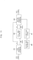
- FIG 10 is a block diagram of the driving controller 200 of a display apparatus.
- the display apparatus and the method of driving the display panel is substantially the same as the display apparatus and the method of driving the display panel explained with reference to FIGS. 1 to 6 except for the structure of the driving controller 200.
- the same reference numerals will be used to refer to the same or like parts as those described in FIGS. 1 to 6 , and any repetitive explanation concerning the above elements will be omitted.
- the driving controller 200 may include the still image determiner 220, the driving frequency determiner 240, and the flicker value storage 260.
- the driving controller 200 may further include the voltage drop determiner 280 and a driving mode setter 298.
- the driving mode setter 298 is shown to be included in the driving controller 200, the present inventive concept is not limited thereto.
- the driving mode setter 298 is disposed external to the driving controller 200.
- the driving mode setter 298 may adjust the flicker value based on a driving mode.
- the driving mode may be automatically set according to the input image data IMG
- the luminance of the display image may vary.
- the just-noticeable difference of the user may vary as well.
- the driving mode setter 298 may determine the just-noticeable difference according to the driving mode.
- the flicker value may be adjusted according to the just-noticeable difference determined by the driving mode setter 298.
- the driving mode setter 298 may set a reference just-noticeable difference to be little.
- the reference just-noticeable difference may be inversely proportional to the maximum luminance of the display image.
- a size of the low driving grayscale range may be little.
- the driving mode setter 298 may set a reference just-noticeable difference to be great.
- a size of the low driving grayscale range may be great.
- the flicker value is adjusted based on the just-noticeable difference of the user according to the voltage drop and the just-noticeable difference of the user according to the driving mode.
- the driving mode setter 298 may determine whether a high dynamic range (HDR) mode is enabled or not.
- HDR high dynamic range
- the display panel 100 may display a bright portion of the display image to be brighter and a dark portion of the display image to be darker.
- the maximum luminance of the display image increases, so that the reference just-noticeable difference may be set to be little.
- the reference just-noticeable difference may be set to be great.
- the display apparatus determines the driving frequency according to the image displayed on the display panel 100 to reduce the power consumption of the display apparatus.
- the driving frequency may be determined using the flicker value of the image on the display panel 100 to prevent the flicker of the image and enhance the display quality of the display panel 100.
- the display apparatus includes the voltage drop determiner 280 for adjusting the flicker value based on the voltage drop of the display panel and the driving mode setter 298 for adjusting the flicker value based on the driving mode.
- FIG 11 is a block diagram of the driving controller 200 of a display apparatus.
- FIG 12 is a timing diagram of a vertical synchronizing signal, a horizontal synchronizing signal, and a data enable signal in a frame.
- the display apparatus and the method of driving the display panel is substantially the same as the display apparatus and the method of driving the display panel explained with reference to FIGS. 1 to 6 except for the structure of the driving controller 200.
- the same reference numerals will be used to refer to the same or like parts as those described in FIGS. 1 to 6 , and any repetitive explanation concerning the above elements will be omitted.
- the driving controller 200 may include the still image determiner 220, the driving frequency determiner 240, and the flicker value storage 260.
- the driving controller 200 may further include the voltage drop determiner 280 and a fixed frequency determiner 210.
- the fixed frequency determiner 210 is shown to be included in the driving controller 200, the present inventive concept may not be limited thereto.
- the fixed frequency determiner 210 may be disposed external to the driving controller 200.
- the fixed frequency determiner 210 may determine whether an input frequency of the input image data IMG has a normal type. For example, the fixed frequency determiner 210 may determine whether the input frequency of the input image data IMG has the normal type by counting the number of pulses of a horizontal synchronizing signal HSYNC between a first pulse and a second pulse of a vertical synchronizing signal VSYNC or by counting the number of pulses of a data enable signal DE between the first pulse and the second pulse of the vertical synchronizing signal VSYNC.
- a time duration between the first pulse and the second pulse of the vertical synchronizing signal VSYNC may be defined as a frame (or an image frame).
- the number of the pulses of the horizontal synchronizing signal HSYNC between the first pulse and the second pulse of the vertical synchronizing signal VSYNC may be equal to or greater than 60.
- the number of the pulses of the data enable signal DE between the first pulse and the second pulse of the vertical synchronizing signal VSYNC may be 60.
- the fixed frequency determiner 210 may determine that the input frequency of the input image data IMG has the normal type. In contrast, when the number of the pulses of the data enable signal DE between the first pulse and the second pulse of the vertical synchronizing signal VSYNC is not equal to the input frequency of the input image data IMG, the fixed frequency determiner 210 may determine that the input frequency of the input image data IMG does not have the normal type.
- the fixed frequency determiner 210 may generate a frequency flag FF that represents whether the input frequency of the input image data IMG has the normal type or not.
- the fixed frequency determiner 210 may output the frequency flag FF to the driving frequency determiner 240.
- the driving frequency determiner 240 may determine the driving frequency of the display panel 100 based on the frequency flag FF. For example, when the input frequency of the input image data IMG does not have the normal type, the driving frequency determiner 240 may drive the switching elements in the pixel P in the normal driving frequency. When the input frequency of the input image data IMG does not have the normal type and the display panel 100 is driven at the low driving frequency, the display panel 100 may generate a display defect.
- the still image determiner 220 may not operate when the input frequency of the input image data IMG does not have the normal type, because the driving frequency is fixed to the normal driving frequency when the input frequency of the input image data IMG does not have the normal type.
- the still image determiner 220 may determine whether the input image data IMG is a still image or a video image.
- the still image determiner 220 may output a flag SF that represents whether the input image data IMG is the still image or the video image to the driving frequency determiner 240. For example, when the input image data IMG is the still image, the still image determiner 220 may output the flag SF of 1 to the driving frequency determiner 240. When the input image data IMG is the video image, the still image determiner 220 may output the flag SF of 0 to the driving frequency determiner 240. When the display panel 100 operates in an always-on mode, the still image determiner 220 may output the flag SF of 1 to the driving frequency determiner 240.
- the driving frequency determiner 240 may drive the switching elements in the pixel in the low driving frequency.
- the driving frequency determiner 240 may drive the switching elements in the pixel in the normal driving frequency.
- the display apparatus determines the driving frequency according to the image displayed on the display panel 100 to reduce the power consumption of the display apparatus.
- the driving frequency is determined using the flicker value of the image on the display panel 100 to prevent the flicker of the image and enhance the display quality of the display panel 100.
- FIG 13 is a conceptual diagram illustrating a display panel 100 of a display apparatus.
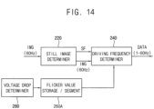
- FIG 14 is a block diagram of the driving controller 200 of the display apparatus of FIG 13 .
- the display apparatus and the method of driving the display panel is substantially the same as the display apparatus and the method of driving the display panel explained with reference to FIGS. 1 to 6 except that the display panel 100 is divided into a plurality of segments.
- the same reference numerals will be used to refer to the same or like parts as those described in FIGS. 1 to 6 , and any repetitive explanation concerning the above elements will be omitted.
- the display apparatus includes the display panel 100 and a display panel driver.
- the display panel 100 may include a plurality of segments SEG11 to SEG85. Although the display panel 100 is shown to include the segments in an eight by five matrix, the present inventive concept is not limited thereto. The display panel 100 including 40 segments in an eight by five matrix is illustrated for convenience of explanation, but the display panel 100 may include a different number of segments.
- the flicker value may be determined for a unit of pixels.
- the entire display panel may be driven at a high driving frequency to prevent the flicker in the one pixel.
- the display panel 100 may be driven at the driving frequency of 30Hz, and the power consumption of the display apparatus may be higher than necessary.
- the display panel 100 determines the flicker value for a unit of segments. If only one pixel in a segment has a high flicker value but remaining pixels in the segment has low flicker values, the flicker value of the segment is determined as an average value of the flicker values in the pixels in the same segment, and the driving frequency of the pixels in the segment is determined using the average value of the flicker values for the pixels in the segment.
- the display panel 100 may be driven at the driving frequency of 1Hz or 2Hz based on the average value of the flicker values in the pixels in the segment, which is less than the driving frequency of 30Hz.
- the display panel 100 is divided into the segments, and the flicker value is determined for a unit of the segment, the power consumption of the display apparatus may be effectively reduced.
- the driving controller 200 may determine optimal driving frequencies for the segments and may determine the maximum driving frequency among the optimal driving frequencies for the segments as the low driving frequency of the display panel 100.
- the driving controller 200 may use the low driving frequency to 10Hz.
- the driving controller 200 includes the still image determiner 220, the driving frequency determiner 240, a flicker value storage 260A, and the voltage drop determiner 280.
- the driving frequency determiner 240 may refer the flicker value storage 260A and information of the segment of the display panel 100 to determine the low driving frequency.
- the flicker value storage 260A may store the grayscale value of the input image data IMG and the flicker value corresponding to the grayscale value of the input image data IMG The flicker value may be used for determining the driving frequency of the display panel 100.
- the flicker value storage 260A may include a lookup table.
- the voltage drop determiner 280 may adjust the flicker value based on a voltage drop of the display panel 100.
- the voltage drop determiner 280 may determine the just-noticeable difference of the user according to the voltage drop of the display panel. In addition, the flicker value may be adjusted according to the just-noticeable difference.
- the voltage drop determiner 280 may set a reference just-noticeable difference to be little.
- a size of the low driving grayscale range may be little.
- the voltage drop determiner 280 may set the reference just-noticeable difference to be great.
- the just-noticeable difference is great, a size of the low driving grayscale range may be great.
- the display panel 100 determines the driving frequency according to the image displayed on the display panel 100 to reduce the power consumption of the display apparatus.
- the driving frequency may be determined using the flicker value of the image on the display panel 100 to prevent the flicker of the image and enhance the display quality of the display panel 100.
- a high frequency driving grayscale area that is driven at the high driving frequency may be decreased by adjusting the driving frequency based on segments to further reduce the power consumption of the display apparatus while effectively preventing the flicker.
- the power consumption of the display apparatus may be reduced, and the display quality of the display panel may be enhanced.
Landscapes
- Engineering & Computer Science (AREA)
- Physics & Mathematics (AREA)
- Computer Hardware Design (AREA)
- General Physics & Mathematics (AREA)
- Theoretical Computer Science (AREA)
- Liquid Crystal Display Device Control (AREA)
- Control Of Indicators Other Than Cathode Ray Tubes (AREA)
- Transforming Electric Information Into Light Information (AREA)
Claims (2)
- Anzeigeeinrichtung, umfassend:ein Anzeigefeld (100), umfassend eine Datenleitung (DL) und ein Pixel, das mit der Datenleitung (DL) verbunden ist, und das dazu konfiguriert ist, ein Bild auf Grundlage von Eingabebilddaten (IMG) anzuzeigen;einen Datentreiber (500), der dazu konfiguriert ist, eine Datenspannung an die Datenleitung (DL) auszugeben; undeine Antriebssteuerung (200), die dazu konfiguriert ist, einen Betrieb des Datentreibers (500) zu steuern und eine Antriebsfrequenz des Anzeigefelds (100) auf Grundlage der Eingabebilddaten (IMG) zu bestimmen,wobei die Antriebssteuerung (200) Folgendes umfasst:einen Flimmerwertspeicher (260), der dazu konfiguriert ist, eine Vielzahl von Flimmer-Lookup-Tabellen zu speichern, wobei die Vielzahl von Flimmer-Lookup-Tabellen eine erste Flimmer-Lookup-Tabelle und eine zweite Flimmer-Lookup-Tabelle umfasst, die sich von der ersten Flimmer-Lookup-Tabelle unterscheidet,wobei jede der Vielzahl von Flimmer-Lookup-Tabellen Flimmerwerte umfasst, die Graustufenwerten der Eingabebilddaten (IMG) entsprechen, undwobei die Flimmerwerte jeweils einen Grad eines von einem Benutzer wahrgenommenen Flimmerns für die Graustufenwerte darstellen;einen Spannungsabfallbestimmer (280), der dazu konfiguriert ist, einen Spannungsabfall einer Datenspannung zu bestimmen, die dem Pixel durch die Datenleitung (DL) zugeführt wird;einen Standbildbestimmer (220), der dazu konfiguriert ist, zu bestimmen, ob die Eingabebilddaten (IMG) ein Standbild oder ein Videobild sind; undeinen Antriebsfrequenzbestimmer (240), der dazu konfiguriert ist, die Antriebsfrequenz des Anzeigefelds (100) zu bestimmen, wenn der Standbildbestimmer (220) bestimmt, dass die Eingabebilddaten (IMG) das Standbild sind,wobei der Spannungsabfallbestimmer (280) dazu konfiguriert ist, eine gerade noch wahrnehmbare Referenzdifferenz gemäß dem bestimmten Spannungsabfall zu bestimmen,wobei der Antriebsfrequenzbestimmer (240) dazu konfiguriert ist, die Antriebsfrequenz gemäß den Flimmerwerten, die den Graustufenwerten der Eingabebilddaten (IMG) entsprechen, unter Verwendung der ersten Flimmer-Lookup-Tabelle zu bestimmen, wenn die bestimmte gerade noch wahrnehmbare Referenzdifferenz eine erste gerade noch wahrnehmbare Differenz ist, undwobei der Antriebsfrequenzbestimmer (240) dazu konfiguriert ist, die Antriebsfrequenz gemäß den Flimmerwerten, die den Graustufenwerten der Eingabebilddaten (IMG) entsprechen, unter Verwendung der zweiten Flimmer-Lookup-Tabelle zu bestimmen, wenn die bestimmte gerade noch wahrnehmbare Referenzdifferenz eine zweite gerade noch wahrnehmbare Differenz ist.
- Anzeigevorrichtung nach Anspruch 1, wobei das Anzeigefeld (100) eine Vielzahl von Segmenten umfasst und wobei die Antriebssteuerung (200) dazu konfiguriert ist, die Antriebsfrequenz des Anzeigefelds (100) auf Grundlage der Vielzahl von Segmenten zu bestimmen.
Applications Claiming Priority (1)
| Application Number | Priority Date | Filing Date | Title |
|---|---|---|---|
| KR1020190120866A KR102702294B1 (ko) | 2019-09-30 | 2019-09-30 | 표시 장치 및 이를 이용한 표시 패널의 구동 방법 |
Publications (3)
| Publication Number | Publication Date |
|---|---|
| EP3799019A2 EP3799019A2 (de) | 2021-03-31 |
| EP3799019A3 EP3799019A3 (de) | 2021-06-02 |
| EP3799019B1 true EP3799019B1 (de) | 2024-05-15 |
Family
ID=72517171
Family Applications (1)
| Application Number | Title | Priority Date | Filing Date |
|---|---|---|---|
| EP20196142.2A Active EP3799019B1 (de) | 2019-09-30 | 2020-09-15 | Anzeigevorrichtung |
Country Status (4)
| Country | Link |
|---|---|
| US (2) | US11462145B2 (de) |
| EP (1) | EP3799019B1 (de) |
| KR (1) | KR102702294B1 (de) |
| CN (1) | CN112581895B (de) |
Families Citing this family (4)
| Publication number | Priority date | Publication date | Assignee | Title |
|---|---|---|---|---|
| US20240279249A1 (en) | 2021-03-25 | 2024-08-22 | Lg Chem, Ltd. | Compound, Coating Composition Comprising Same, Organic Light-Emitting Device Using Same, and Manufacturing Method Therefor |
| US12531004B2 (en) | 2023-04-09 | 2026-01-20 | Novatek Microelectronics Corp. | Display device and grayscale compensation method thereof |
| US12374260B2 (en) * | 2023-04-09 | 2025-07-29 | Novatek Microelectronics Corp. | Display device and grayscale compensation method thereof |
| CN119252198B (zh) * | 2024-10-17 | 2026-04-10 | 广州华星光电半导体显示技术有限公司 | 显示装置及其驱动方法 |
Family Cites Families (15)
| Publication number | Priority date | Publication date | Assignee | Title |
|---|---|---|---|---|
| JP3789113B2 (ja) * | 2003-01-17 | 2006-06-21 | キヤノン株式会社 | 画像表示装置 |
| KR101256665B1 (ko) * | 2005-12-30 | 2013-04-19 | 엘지디스플레이 주식회사 | 액정패널 |
| KR20080098097A (ko) | 2007-05-04 | 2008-11-07 | 엘지이노텍 주식회사 | 액정패널의 자동화질개선장치 및 그 동작방법 |
| US9280943B2 (en) * | 2009-02-13 | 2016-03-08 | Barco, N.V. | Devices and methods for reducing artefacts in display devices by the use of overdrive |
| JP6253894B2 (ja) * | 2013-04-18 | 2017-12-27 | シャープ株式会社 | 制御装置、表示装置および制御方法 |
| KR102174236B1 (ko) * | 2014-02-11 | 2020-11-05 | 삼성디스플레이 주식회사 | 표시 패널의 구동 방법 및 이를 수행하기 위한 표시 장치 |
| KR102128969B1 (ko) * | 2014-02-17 | 2020-07-02 | 삼성디스플레이 주식회사 | 액정 표시 장치 및 그 제조 방법 |
| US10008182B2 (en) * | 2014-09-12 | 2018-06-26 | Samsung Electronics Co., Ltd. | System-on-chip (SoC) devices, display drivers and SoC systems including the same |
| FR3025921A1 (fr) * | 2014-09-15 | 2016-03-18 | St Microelectronics Int Nv | Procede de determination d'une frequence de rafraichissement d'une matrice de pixels actifs oled, et dispositif correspondant |
| KR102251686B1 (ko) | 2014-10-14 | 2021-05-14 | 삼성디스플레이 주식회사 | 표시 패널의 구동 방법 및 이를 수행하는 표시 장치 |
| KR102253677B1 (ko) | 2014-11-04 | 2021-05-21 | 엘지디스플레이 주식회사 | 표시장치와 이의 구동방법 |
| KR102353218B1 (ko) * | 2015-07-15 | 2022-01-20 | 삼성디스플레이 주식회사 | 표시 장치 및 그것의 구동 방법 |
| CN106531105B (zh) * | 2016-12-26 | 2019-06-28 | 上海天马微电子有限公司 | 显示面板的驱动方法及显示面板 |
| CN106652915A (zh) * | 2017-02-09 | 2017-05-10 | 鄂尔多斯市源盛光电有限责任公司 | 一种像素电路、显示面板、显示装置及驱动方法 |
| CN206877668U (zh) * | 2017-05-26 | 2018-01-12 | 维沃移动通信有限公司 | 一种显示屏亮度调节电路以及移动终端 |
-
2019
- 2019-09-30 KR KR1020190120866A patent/KR102702294B1/ko active Active
-
2020
- 2020-08-12 US US16/992,011 patent/US11462145B2/en active Active
- 2020-09-15 EP EP20196142.2A patent/EP3799019B1/de active Active
- 2020-09-28 CN CN202011039960.0A patent/CN112581895B/zh active Active
-
2022
- 2022-09-08 US US17/940,414 patent/US11817030B2/en active Active
Also Published As
| Publication number | Publication date |
|---|---|
| CN112581895A (zh) | 2021-03-30 |
| US20210097924A1 (en) | 2021-04-01 |
| KR20210038765A (ko) | 2021-04-08 |
| EP3799019A3 (de) | 2021-06-02 |
| CN112581895B (zh) | 2025-09-12 |
| KR102702294B1 (ko) | 2024-09-04 |
| US11817030B2 (en) | 2023-11-14 |
| EP3799019A2 (de) | 2021-03-31 |
| US20230005409A1 (en) | 2023-01-05 |
| US11462145B2 (en) | 2022-10-04 |
Similar Documents
| Publication | Publication Date | Title |
|---|---|---|
| EP3799019B1 (de) | Anzeigevorrichtung | |
| CN111833802B (zh) | 显示装置 | |
| US7394448B2 (en) | Method and apparatus for driving liquid crystal display device | |
| CN101188093B (zh) | 液晶显示器及其驱动方法 | |
| US9564085B2 (en) | Selective dimming to reduce power of a light emitting display device | |
| KR102807253B1 (ko) | 표시 장치 및 이를 이용한 표시 패널의 구동 방법 | |
| KR102713880B1 (ko) | 표시 장치와 그 구동 방법 | |
| US20160196802A1 (en) | Low-Flicker Variable Refresh Rate Display | |
| KR101978797B1 (ko) | 유기발광 표시장치 및 이의 구동방법 | |
| JP2002323876A (ja) | 液晶表示装置における画像表示方法及び液晶表示装置 | |
| CN112397003B (zh) | 显示装置及其驱动方法 | |
| CN116013179A (zh) | 显示装置 | |
| CN112419974A (zh) | 显示装置和驱动显示装置的显示面板的方法 | |
| KR102059501B1 (ko) | 표시 장치 및 그 구동 방법 | |
| US11189238B2 (en) | Display device and electronic device | |
| CN114067716A (zh) | 柔性显示装置以及利用其的显示面板的驱动方法 | |
| JP2012058351A (ja) | 画像表示装置 | |
| JP7840557B2 (ja) | 電流制限回路、表示装置、及び、電流制限方法 | |
| KR102413473B1 (ko) | 표시 장치의 구동 방법 | |
| KR101287202B1 (ko) | 화상 표시장치 | |
| JP2007041591A (ja) | 表示装置 | |
| KR102882167B1 (ko) | 구동 제어부, 이를 포함하는 표시 장치 및 이를 이용한 표시 패널의 구동 방법 | |
| KR101351888B1 (ko) | 액정표시장치와 그 구동방법 | |
| KR102753739B1 (ko) | 표시 장치 | |
| KR20100090476A (ko) | 표시 패널의 구동 방법 및 이를 수행하기 위한 표시 장치 |
Legal Events
| Date | Code | Title | Description |
|---|---|---|---|
| PUAI | Public reference made under article 153(3) epc to a published international application that has entered the european phase |
Free format text: ORIGINAL CODE: 0009012 |
|
| STAA | Information on the status of an ep patent application or granted ep patent |
Free format text: STATUS: THE APPLICATION HAS BEEN PUBLISHED |
|
| AK | Designated contracting states |
Kind code of ref document: A2 Designated state(s): AL AT BE BG CH CY CZ DE DK EE ES FI FR GB GR HR HU IE IS IT LI LT LU LV MC MK MT NL NO PL PT RO RS SE SI SK SM TR |
|
| AX | Request for extension of the european patent |
Extension state: BA ME |
|
| PUAL | Search report despatched |
Free format text: ORIGINAL CODE: 0009013 |
|
| AK | Designated contracting states |
Kind code of ref document: A3 Designated state(s): AL AT BE BG CH CY CZ DE DK EE ES FI FR GB GR HR HU IE IS IT LI LT LU LV MC MK MT NL NO PL PT RO RS SE SI SK SM TR |
|
| RIC1 | Information provided on ipc code assigned before grant |
Ipc: G09G 3/20 20060101AFI20210427BHEP |
|
| STAA | Information on the status of an ep patent application or granted ep patent |
Free format text: STATUS: REQUEST FOR EXAMINATION WAS MADE |
|
| 17P | Request for examination filed |
Effective date: 20211129 |
|
| RBV | Designated contracting states (corrected) |
Designated state(s): AL AT BE BG CH CY CZ DE DK EE ES FI FR GB GR HR HU IE IS IT LI LT LU LV MC MK MT NL NO PL PT RO RS SE SI SK SM TR |
|
| STAA | Information on the status of an ep patent application or granted ep patent |
Free format text: STATUS: EXAMINATION IS IN PROGRESS |
|
| 17Q | First examination report despatched |
Effective date: 20230217 |
|
| P01 | Opt-out of the competence of the unified patent court (upc) registered |
Effective date: 20230516 |
|
| GRAP | Despatch of communication of intention to grant a patent |
Free format text: ORIGINAL CODE: EPIDOSNIGR1 |
|
| STAA | Information on the status of an ep patent application or granted ep patent |
Free format text: STATUS: GRANT OF PATENT IS INTENDED |
|
| INTG | Intention to grant announced |
Effective date: 20240111 |
|
| GRAS | Grant fee paid |
Free format text: ORIGINAL CODE: EPIDOSNIGR3 |
|
| GRAA | (expected) grant |
Free format text: ORIGINAL CODE: 0009210 |
|
| STAA | Information on the status of an ep patent application or granted ep patent |
Free format text: STATUS: THE PATENT HAS BEEN GRANTED |
|
| AK | Designated contracting states |
Kind code of ref document: B1 Designated state(s): AL AT BE BG CH CY CZ DE DK EE ES FI FR GB GR HR HU IE IS IT LI LT LU LV MC MK MT NL NO PL PT RO RS SE SI SK SM TR |
|
| REG | Reference to a national code |
Ref country code: CH Ref legal event code: EP |
|
| REG | Reference to a national code |
Ref country code: DE Ref legal event code: R096 Ref document number: 602020030850 Country of ref document: DE |
|
| REG | Reference to a national code |
Ref country code: IE Ref legal event code: FG4D |
|
| REG | Reference to a national code |
Ref country code: LT Ref legal event code: MG9D |
|
| REG | Reference to a national code |
Ref country code: NL Ref legal event code: MP Effective date: 20240515 |
|
| PG25 | Lapsed in a contracting state [announced via postgrant information from national office to epo] |
Ref country code: IS Free format text: LAPSE BECAUSE OF FAILURE TO SUBMIT A TRANSLATION OF THE DESCRIPTION OR TO PAY THE FEE WITHIN THE PRESCRIBED TIME-LIMIT Effective date: 20240915 |
|
| PG25 | Lapsed in a contracting state [announced via postgrant information from national office to epo] |
Ref country code: BG Free format text: LAPSE BECAUSE OF FAILURE TO SUBMIT A TRANSLATION OF THE DESCRIPTION OR TO PAY THE FEE WITHIN THE PRESCRIBED TIME-LIMIT Effective date: 20240515 |
|
| PG25 | Lapsed in a contracting state [announced via postgrant information from national office to epo] |
Ref country code: FI Free format text: LAPSE BECAUSE OF FAILURE TO SUBMIT A TRANSLATION OF THE DESCRIPTION OR TO PAY THE FEE WITHIN THE PRESCRIBED TIME-LIMIT Effective date: 20240515 Ref country code: HR Free format text: LAPSE BECAUSE OF FAILURE TO SUBMIT A TRANSLATION OF THE DESCRIPTION OR TO PAY THE FEE WITHIN THE PRESCRIBED TIME-LIMIT Effective date: 20240515 |
|
| PG25 | Lapsed in a contracting state [announced via postgrant information from national office to epo] |
Ref country code: GR Free format text: LAPSE BECAUSE OF FAILURE TO SUBMIT A TRANSLATION OF THE DESCRIPTION OR TO PAY THE FEE WITHIN THE PRESCRIBED TIME-LIMIT Effective date: 20240816 |
|
| PG25 | Lapsed in a contracting state [announced via postgrant information from national office to epo] |
Ref country code: PT Free format text: LAPSE BECAUSE OF FAILURE TO SUBMIT A TRANSLATION OF THE DESCRIPTION OR TO PAY THE FEE WITHIN THE PRESCRIBED TIME-LIMIT Effective date: 20240916 |
|
| REG | Reference to a national code |
Ref country code: AT Ref legal event code: MK05 Ref document number: 1687565 Country of ref document: AT Kind code of ref document: T Effective date: 20240515 |
|
| PG25 | Lapsed in a contracting state [announced via postgrant information from national office to epo] |
Ref country code: NL Free format text: LAPSE BECAUSE OF FAILURE TO SUBMIT A TRANSLATION OF THE DESCRIPTION OR TO PAY THE FEE WITHIN THE PRESCRIBED TIME-LIMIT Effective date: 20240515 |
|
| PG25 | Lapsed in a contracting state [announced via postgrant information from national office to epo] |
Ref country code: ES Free format text: LAPSE BECAUSE OF FAILURE TO SUBMIT A TRANSLATION OF THE DESCRIPTION OR TO PAY THE FEE WITHIN THE PRESCRIBED TIME-LIMIT Effective date: 20240515 |
|
| PG25 | Lapsed in a contracting state [announced via postgrant information from national office to epo] |
Ref country code: AT Free format text: LAPSE BECAUSE OF FAILURE TO SUBMIT A TRANSLATION OF THE DESCRIPTION OR TO PAY THE FEE WITHIN THE PRESCRIBED TIME-LIMIT Effective date: 20240515 |
|
| PG25 | Lapsed in a contracting state [announced via postgrant information from national office to epo] |
Ref country code: PL Free format text: LAPSE BECAUSE OF FAILURE TO SUBMIT A TRANSLATION OF THE DESCRIPTION OR TO PAY THE FEE WITHIN THE PRESCRIBED TIME-LIMIT Effective date: 20240515 |
|
| PG25 | Lapsed in a contracting state [announced via postgrant information from national office to epo] |
Ref country code: LV Free format text: LAPSE BECAUSE OF FAILURE TO SUBMIT A TRANSLATION OF THE DESCRIPTION OR TO PAY THE FEE WITHIN THE PRESCRIBED TIME-LIMIT Effective date: 20240515 |
|
| PG25 | Lapsed in a contracting state [announced via postgrant information from national office to epo] |
Ref country code: PT Free format text: LAPSE BECAUSE OF FAILURE TO SUBMIT A TRANSLATION OF THE DESCRIPTION OR TO PAY THE FEE WITHIN THE PRESCRIBED TIME-LIMIT Effective date: 20240916 Ref country code: PL Free format text: LAPSE BECAUSE OF FAILURE TO SUBMIT A TRANSLATION OF THE DESCRIPTION OR TO PAY THE FEE WITHIN THE PRESCRIBED TIME-LIMIT Effective date: 20240515 Ref country code: NO Free format text: LAPSE BECAUSE OF FAILURE TO SUBMIT A TRANSLATION OF THE DESCRIPTION OR TO PAY THE FEE WITHIN THE PRESCRIBED TIME-LIMIT Effective date: 20240815 Ref country code: NL Free format text: LAPSE BECAUSE OF FAILURE TO SUBMIT A TRANSLATION OF THE DESCRIPTION OR TO PAY THE FEE WITHIN THE PRESCRIBED TIME-LIMIT Effective date: 20240515 Ref country code: LV Free format text: LAPSE BECAUSE OF FAILURE TO SUBMIT A TRANSLATION OF THE DESCRIPTION OR TO PAY THE FEE WITHIN THE PRESCRIBED TIME-LIMIT Effective date: 20240515 Ref country code: IS Free format text: LAPSE BECAUSE OF FAILURE TO SUBMIT A TRANSLATION OF THE DESCRIPTION OR TO PAY THE FEE WITHIN THE PRESCRIBED TIME-LIMIT Effective date: 20240915 Ref country code: HR Free format text: LAPSE BECAUSE OF FAILURE TO SUBMIT A TRANSLATION OF THE DESCRIPTION OR TO PAY THE FEE WITHIN THE PRESCRIBED TIME-LIMIT Effective date: 20240515 Ref country code: GR Free format text: LAPSE BECAUSE OF FAILURE TO SUBMIT A TRANSLATION OF THE DESCRIPTION OR TO PAY THE FEE WITHIN THE PRESCRIBED TIME-LIMIT Effective date: 20240816 Ref country code: FI Free format text: LAPSE BECAUSE OF FAILURE TO SUBMIT A TRANSLATION OF THE DESCRIPTION OR TO PAY THE FEE WITHIN THE PRESCRIBED TIME-LIMIT Effective date: 20240515 Ref country code: ES Free format text: LAPSE BECAUSE OF FAILURE TO SUBMIT A TRANSLATION OF THE DESCRIPTION OR TO PAY THE FEE WITHIN THE PRESCRIBED TIME-LIMIT Effective date: 20240515 Ref country code: BG Free format text: LAPSE BECAUSE OF FAILURE TO SUBMIT A TRANSLATION OF THE DESCRIPTION OR TO PAY THE FEE WITHIN THE PRESCRIBED TIME-LIMIT Effective date: 20240515 Ref country code: AT Free format text: LAPSE BECAUSE OF FAILURE TO SUBMIT A TRANSLATION OF THE DESCRIPTION OR TO PAY THE FEE WITHIN THE PRESCRIBED TIME-LIMIT Effective date: 20240515 Ref country code: RS Free format text: LAPSE BECAUSE OF FAILURE TO SUBMIT A TRANSLATION OF THE DESCRIPTION OR TO PAY THE FEE WITHIN THE PRESCRIBED TIME-LIMIT Effective date: 20240815 |
|
| PG25 | Lapsed in a contracting state [announced via postgrant information from national office to epo] |
Ref country code: DK Free format text: LAPSE BECAUSE OF FAILURE TO SUBMIT A TRANSLATION OF THE DESCRIPTION OR TO PAY THE FEE WITHIN THE PRESCRIBED TIME-LIMIT Effective date: 20240515 |
|
| PG25 | Lapsed in a contracting state [announced via postgrant information from national office to epo] |
Ref country code: EE Free format text: LAPSE BECAUSE OF FAILURE TO SUBMIT A TRANSLATION OF THE DESCRIPTION OR TO PAY THE FEE WITHIN THE PRESCRIBED TIME-LIMIT Effective date: 20240515 |
|
| PG25 | Lapsed in a contracting state [announced via postgrant information from national office to epo] |
Ref country code: CZ Free format text: LAPSE BECAUSE OF FAILURE TO SUBMIT A TRANSLATION OF THE DESCRIPTION OR TO PAY THE FEE WITHIN THE PRESCRIBED TIME-LIMIT Effective date: 20240515 |
|
| PG25 | Lapsed in a contracting state [announced via postgrant information from national office to epo] |
Ref country code: RO Free format text: LAPSE BECAUSE OF FAILURE TO SUBMIT A TRANSLATION OF THE DESCRIPTION OR TO PAY THE FEE WITHIN THE PRESCRIBED TIME-LIMIT Effective date: 20240515 Ref country code: SK Free format text: LAPSE BECAUSE OF FAILURE TO SUBMIT A TRANSLATION OF THE DESCRIPTION OR TO PAY THE FEE WITHIN THE PRESCRIBED TIME-LIMIT Effective date: 20240515 |
|
| PG25 | Lapsed in a contracting state [announced via postgrant information from national office to epo] |
Ref country code: SM Free format text: LAPSE BECAUSE OF FAILURE TO SUBMIT A TRANSLATION OF THE DESCRIPTION OR TO PAY THE FEE WITHIN THE PRESCRIBED TIME-LIMIT Effective date: 20240515 |
|
| PG25 | Lapsed in a contracting state [announced via postgrant information from national office to epo] |
Ref country code: SM Free format text: LAPSE BECAUSE OF FAILURE TO SUBMIT A TRANSLATION OF THE DESCRIPTION OR TO PAY THE FEE WITHIN THE PRESCRIBED TIME-LIMIT Effective date: 20240515 Ref country code: SK Free format text: LAPSE BECAUSE OF FAILURE TO SUBMIT A TRANSLATION OF THE DESCRIPTION OR TO PAY THE FEE WITHIN THE PRESCRIBED TIME-LIMIT Effective date: 20240515 Ref country code: RO Free format text: LAPSE BECAUSE OF FAILURE TO SUBMIT A TRANSLATION OF THE DESCRIPTION OR TO PAY THE FEE WITHIN THE PRESCRIBED TIME-LIMIT Effective date: 20240515 Ref country code: EE Free format text: LAPSE BECAUSE OF FAILURE TO SUBMIT A TRANSLATION OF THE DESCRIPTION OR TO PAY THE FEE WITHIN THE PRESCRIBED TIME-LIMIT Effective date: 20240515 Ref country code: DK Free format text: LAPSE BECAUSE OF FAILURE TO SUBMIT A TRANSLATION OF THE DESCRIPTION OR TO PAY THE FEE WITHIN THE PRESCRIBED TIME-LIMIT Effective date: 20240515 Ref country code: CZ Free format text: LAPSE BECAUSE OF FAILURE TO SUBMIT A TRANSLATION OF THE DESCRIPTION OR TO PAY THE FEE WITHIN THE PRESCRIBED TIME-LIMIT Effective date: 20240515 |
|
| PG25 | Lapsed in a contracting state [announced via postgrant information from national office to epo] |
Ref country code: IT Free format text: LAPSE BECAUSE OF FAILURE TO SUBMIT A TRANSLATION OF THE DESCRIPTION OR TO PAY THE FEE WITHIN THE PRESCRIBED TIME-LIMIT Effective date: 20240515 |
|
| REG | Reference to a national code |
Ref country code: DE Ref legal event code: R097 Ref document number: 602020030850 Country of ref document: DE |
|
| PLBE | No opposition filed within time limit |
Free format text: ORIGINAL CODE: 0009261 |
|
| STAA | Information on the status of an ep patent application or granted ep patent |
Free format text: STATUS: NO OPPOSITION FILED WITHIN TIME LIMIT |
|
| 26N | No opposition filed |
Effective date: 20250218 |
|
| PG25 | Lapsed in a contracting state [announced via postgrant information from national office to epo] |
Ref country code: MC Free format text: LAPSE BECAUSE OF FAILURE TO SUBMIT A TRANSLATION OF THE DESCRIPTION OR TO PAY THE FEE WITHIN THE PRESCRIBED TIME-LIMIT Effective date: 20240515 Ref country code: SI Free format text: LAPSE BECAUSE OF FAILURE TO SUBMIT A TRANSLATION OF THE DESCRIPTION OR TO PAY THE FEE WITHIN THE PRESCRIBED TIME-LIMIT Effective date: 20240515 |
|
| REG | Reference to a national code |
Ref country code: CH Ref legal event code: PL |
|
| PG25 | Lapsed in a contracting state [announced via postgrant information from national office to epo] |
Ref country code: LU Free format text: LAPSE BECAUSE OF NON-PAYMENT OF DUE FEES Effective date: 20240915 |
|
| REG | Reference to a national code |
Ref country code: BE Ref legal event code: MM Effective date: 20240930 |
|
| PG25 | Lapsed in a contracting state [announced via postgrant information from national office to epo] |
Ref country code: BE Free format text: LAPSE BECAUSE OF NON-PAYMENT OF DUE FEES Effective date: 20240930 |
|
| PG25 | Lapsed in a contracting state [announced via postgrant information from national office to epo] |
Ref country code: CH Free format text: LAPSE BECAUSE OF NON-PAYMENT OF DUE FEES Effective date: 20240930 |
|
| PG25 | Lapsed in a contracting state [announced via postgrant information from national office to epo] |
Ref country code: IE Free format text: LAPSE BECAUSE OF NON-PAYMENT OF DUE FEES Effective date: 20240915 |
|
| PG25 | Lapsed in a contracting state [announced via postgrant information from national office to epo] |
Ref country code: SE Free format text: LAPSE BECAUSE OF FAILURE TO SUBMIT A TRANSLATION OF THE DESCRIPTION OR TO PAY THE FEE WITHIN THE PRESCRIBED TIME-LIMIT Effective date: 20240515 |
|
| PGFP | Annual fee paid to national office [announced via postgrant information from national office to epo] |
Ref country code: DE Payment date: 20250820 Year of fee payment: 6 |
|
| PGFP | Annual fee paid to national office [announced via postgrant information from national office to epo] |
Ref country code: GB Payment date: 20250820 Year of fee payment: 6 |
|
| PGFP | Annual fee paid to national office [announced via postgrant information from national office to epo] |
Ref country code: FR Payment date: 20250821 Year of fee payment: 6 |
|
| PG25 | Lapsed in a contracting state [announced via postgrant information from national office to epo] |
Ref country code: CY Free format text: LAPSE BECAUSE OF FAILURE TO SUBMIT A TRANSLATION OF THE DESCRIPTION OR TO PAY THE FEE WITHIN THE PRESCRIBED TIME-LIMIT; INVALID AB INITIO Effective date: 20200915 |
|
| PG25 | Lapsed in a contracting state [announced via postgrant information from national office to epo] |
Ref country code: HU Free format text: LAPSE BECAUSE OF FAILURE TO SUBMIT A TRANSLATION OF THE DESCRIPTION OR TO PAY THE FEE WITHIN THE PRESCRIBED TIME-LIMIT; INVALID AB INITIO Effective date: 20200915 |