EP3796399A1 - Photodetector - Google Patents
Photodetector Download PDFInfo
- Publication number
- EP3796399A1 EP3796399A1 EP19804105.5A EP19804105A EP3796399A1 EP 3796399 A1 EP3796399 A1 EP 3796399A1 EP 19804105 A EP19804105 A EP 19804105A EP 3796399 A1 EP3796399 A1 EP 3796399A1
- Authority
- EP
- European Patent Office
- Prior art keywords
- silicon
- zener diode
- type
- layer
- photodiode
- Prior art date
- Legal status (The legal status is an assumption and is not a legal conclusion. Google has not performed a legal analysis and makes no representation as to the accuracy of the status listed.)
- Granted
Links
Images



Classifications
-
- H—ELECTRICITY
- H10—SEMICONDUCTOR DEVICES; ELECTRIC SOLID-STATE DEVICES NOT OTHERWISE PROVIDED FOR
- H10F—INORGANIC SEMICONDUCTOR DEVICES SENSITIVE TO INFRARED RADIATION, LIGHT, ELECTROMAGNETIC RADIATION OF SHORTER WAVELENGTH OR CORPUSCULAR RADIATION
- H10F30/00—Individual radiation-sensitive semiconductor devices in which radiation controls the flow of current through the devices, e.g. photodetectors
- H10F30/20—Individual radiation-sensitive semiconductor devices in which radiation controls the flow of current through the devices, e.g. photodetectors the devices having potential barriers, e.g. phototransistors
- H10F30/21—Individual radiation-sensitive semiconductor devices in which radiation controls the flow of current through the devices, e.g. photodetectors the devices having potential barriers, e.g. phototransistors the devices being sensitive to infrared, visible or ultraviolet radiation
- H10F30/22—Individual radiation-sensitive semiconductor devices in which radiation controls the flow of current through the devices, e.g. photodetectors the devices having potential barriers, e.g. phototransistors the devices being sensitive to infrared, visible or ultraviolet radiation the devices having only one potential barrier, e.g. photodiodes
- H10F30/223—Individual radiation-sensitive semiconductor devices in which radiation controls the flow of current through the devices, e.g. photodetectors the devices having potential barriers, e.g. phototransistors the devices being sensitive to infrared, visible or ultraviolet radiation the devices having only one potential barrier, e.g. photodiodes the potential barrier being a PIN barrier
-
- H—ELECTRICITY
- H10—SEMICONDUCTOR DEVICES; ELECTRIC SOLID-STATE DEVICES NOT OTHERWISE PROVIDED FOR
- H10D—INORGANIC ELECTRIC SEMICONDUCTOR DEVICES
- H10D8/00—Diodes
- H10D8/20—Breakdown diodes, e.g. avalanche diodes
- H10D8/25—Zener diodes
-
- H—ELECTRICITY
- H10—SEMICONDUCTOR DEVICES; ELECTRIC SOLID-STATE DEVICES NOT OTHERWISE PROVIDED FOR
- H10D—INORGANIC ELECTRIC SEMICONDUCTOR DEVICES
- H10D89/00—Aspects of integrated devices not covered by groups H10D84/00 - H10D88/00
- H10D89/60—Integrated devices comprising arrangements for electrical or thermal protection, e.g. protection circuits against electrostatic discharge [ESD]
-
- H—ELECTRICITY
- H10—SEMICONDUCTOR DEVICES; ELECTRIC SOLID-STATE DEVICES NOT OTHERWISE PROVIDED FOR
- H10F—INORGANIC SEMICONDUCTOR DEVICES SENSITIVE TO INFRARED RADIATION, LIGHT, ELECTROMAGNETIC RADIATION OF SHORTER WAVELENGTH OR CORPUSCULAR RADIATION
- H10F39/00—Integrated devices, or assemblies of multiple devices, comprising at least one element covered by group H10F30/00, e.g. radiation detectors comprising photodiode arrays
- H10F39/10—Integrated devices
- H10F39/103—Integrated devices the at least one element covered by H10F30/00 having potential barriers, e.g. integrated devices comprising photodiodes or phototransistors
-
- H—ELECTRICITY
- H10—SEMICONDUCTOR DEVICES; ELECTRIC SOLID-STATE DEVICES NOT OTHERWISE PROVIDED FOR
- H10F—INORGANIC SEMICONDUCTOR DEVICES SENSITIVE TO INFRARED RADIATION, LIGHT, ELECTROMAGNETIC RADIATION OF SHORTER WAVELENGTH OR CORPUSCULAR RADIATION
- H10F77/00—Constructional details of devices covered by this subclass
- H10F77/10—Semiconductor bodies
- H10F77/12—Active materials
- H10F77/122—Active materials comprising only Group IV materials
-
- H—ELECTRICITY
- H10—SEMICONDUCTOR DEVICES; ELECTRIC SOLID-STATE DEVICES NOT OTHERWISE PROVIDED FOR
- H10F—INORGANIC SEMICONDUCTOR DEVICES SENSITIVE TO INFRARED RADIATION, LIGHT, ELECTROMAGNETIC RADIATION OF SHORTER WAVELENGTH OR CORPUSCULAR RADIATION
- H10F77/00—Constructional details of devices covered by this subclass
- H10F77/40—Optical elements or arrangements
- H10F77/413—Optical elements or arrangements directly associated or integrated with the devices, e.g. back reflectors
-
- H—ELECTRICITY
- H10—SEMICONDUCTOR DEVICES; ELECTRIC SOLID-STATE DEVICES NOT OTHERWISE PROVIDED FOR
- H10D—INORGANIC ELECTRIC SEMICONDUCTOR DEVICES
- H10D62/00—Semiconductor bodies, or regions thereof, of devices having potential barriers
- H10D62/80—Semiconductor bodies, or regions thereof, of devices having potential barriers characterised by the materials
- H10D62/82—Heterojunctions
- H10D62/822—Heterojunctions comprising only Group IV materials heterojunctions, e.g. Si/Ge heterojunctions
-
- H—ELECTRICITY
- H10—SEMICONDUCTOR DEVICES; ELECTRIC SOLID-STATE DEVICES NOT OTHERWISE PROVIDED FOR
- H10D—INORGANIC ELECTRIC SEMICONDUCTOR DEVICES
- H10D89/00—Aspects of integrated devices not covered by groups H10D84/00 - H10D88/00
- H10D89/60—Integrated devices comprising arrangements for electrical or thermal protection, e.g. protection circuits against electrostatic discharge [ESD]
- H10D89/601—Integrated devices comprising arrangements for electrical or thermal protection, e.g. protection circuits against electrostatic discharge [ESD] for devices having insulated gate electrodes, e.g. for IGFETs or IGBTs
- H10D89/611—Integrated devices comprising arrangements for electrical or thermal protection, e.g. protection circuits against electrostatic discharge [ESD] for devices having insulated gate electrodes, e.g. for IGFETs or IGBTs using diodes as protective elements
Definitions
- the present invention relates to a photodetector used in an optical communication system and an optical information processing system, and more particularly to a structure for providing a photodetector excellent in resistance to electrostatic discharge.
- Fig. 1 is a view schematically showing a structure of a conventional waveguide-coupling vertical type GePD.
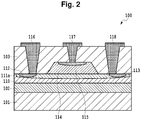
- Fig. 2 is a cross-sectional view taken along the line II-II' of Fig. 1 . It should be noted that in Fig. 1 , in order to make the structure easier to understand, an upper cladding layer 103 and electrodes 116 to 118 shown in Fig.
- Electrodes 116 to 118 are in contact with a p ++ silicon electrode unit 112, a p ++ silicon electrode unit 113, and a n-type Ge region 115 are indicated by squares. These squares indicate the connection surfaces of the electrodes 116 to 118.
- the p ++ silicon electrode unit 112 is also referred to as a p ++ Si electrode unit or a p-type silicon electrode part.
- the GePD is formed on an SOI (Silicon On Insulator) substrate made of a Si substrate, a Si oxide film, and a surface Si layer by using a lithography technique or the like.
- a GePD 100 shown in Fig. 2 is provide with a Si substrate 101, a lower cladding layer 102 made of a Si oxide film on the Si substrate, a core layer 110, a waveguide (silicon waveguide layer) 109 that guides a signal light, a germanium (Ge) layer 114 that absorbs light formed on the core layer 110, and an upper cladding layer 103 formed on the core layer 110 and the Ge layer 114.
- SOI Silicon On Insulator
- a p-type silicon (Si) slab 111a doped with p-type impurity ions, a p ++ silicon electrode unit 112 and a p ++ silicon electrode unit 113 doped with p-type impurities in high concentration and acting as electrodes are formed.
- the Ge layer 114 is stacked by epitaxial growth, and an n-type Ge region 115 doped with n-type impurities is formed on the upper part of the Ge layer 114.
- the electrodes 116 to 118 are provided on the p ++ silicon electrode unit 112, the p ++ silicon electrode unit 113, and the n-type Ge region 115 so as to be in contact therewith.
- Patent Literature 1 Japanese Patent No. 5370857
- a general GePD shown in Fig. 1 and Fig. 2 have a problem that it is vulnerable to electrostatic discharge.
- Electrostatic discharge is a phenomenon in which a high-voltage pulse is instantaneously applied to a device
- general standard models for electrostatic discharge include a charging device model, a machine model, and a human body model.
- a general GePD has a breakdown voltage of approximately 50 to 150 V in a human body model.
- the breakdown voltage in a human body model required for a general device is approximately 250 to 500 V, and the breakdown voltage of GePDs is insufficient.
- Common means to increase the breakdown voltage for electrostatic discharge include addition of a capacitor in parallel, addition of a resistor in series, and addition of a varistor or a Zener diode in parallel.
- the present invention has been made in view of such problems, and an object thereof is to provide a photodetector that is capable of preventing breakdown caused by electrostatic discharge and with which a breakdown voltage can be expected to enhance by at least 100 V.
- the present invention has been made to solve such problems, and is a photodetector provided with a Zener diode that can be monolithically integrated into a general GePD by a silicon photonics technology.
- the Zener diode provided in the present invention has an extremely low capacity and a low series resistance, and has an operation voltage of 0.5 to -7 V, which not only covers the general operation voltage of GePDs, which is from 0 to 3 V, but also protects GePDs because its threshold voltage is as low as -7 V. This prevents deterioration of the high-speed characteristics of GePDs, and with the monolithic integration, an increase in the circuit scale and the number of manufacturing processes is suppressed.
- the photodetector of the present invention has the following structure. As shown in Fig. 3 , a Zener diode 301 made of a germanium and a silicon is connected in parallel to a general GePD 300. The Zener diode connected in the present invention has a cross-sectional structure as shown in Fig. 4 .
- a first aspect of the present invention is a photodetector including a photodiode and a Zener diode, in which the photodiode is provided with an anode electrode and a cathode electrode, and the Zener diode is provided with a silicon substrate; a lower cladding layer on the silicon substrate; a silicon core layer on the lower cladding layer, including a first-type silicon region doped with first-type impurity ions and a second-type silicon region doped with second-type impurity ions; a silicon waveguide layer connected to the silicon core layer; a germanium layer on the silicon core layer; an upper cladding layer on the germanium layer; and an anode electrode and a cathode electrode each connected to either one of the first-type silicon region and the second-type silicon region, and the anode electrode of the Zener diode is connected to the anode electrode of the photodiode, and the cathode electrode of the Zener dio
- a second aspect of the present invention is the photodetector according to the first aspect, in which, in the Zener diode, the second-type silicon region is disposed directly below the germanium layer; an intrinsic silicon region is disposed between a bottom surface of the germanium layer and the first-type silicon region; and the intrinsic silicon region is disposed between the first-type silicon region and the second-type silicon region.
- a third aspect of the present invention is the photodetector according to the first aspect or the second aspect, in which the photodiode is provided with a silicon substrate; a lower cladding layer on the silicon substrate; a silicon core layer on the lower cladding layer, including a first-type silicon slab doped with first-type impurity ions; a silicon waveguide layer connected to the silicon core layer; a germanium layer on the silicon core layer, including a second-type germanium region doped with second-type impurities; an upper cladding layer on the silicon core layer and the germanium layer; and electrodes connected to the first-type silicon slab and the second-type germanium region, respectively.
- a fourth aspect of the present invention is the photodetector according to the third aspect, in which the silicon substrate, the lower cladding layer, the silicon core layer, and the upper cladding layer provided in the photodiode and the Zener diode are shared by the photodiode and the Zener diode.
- a fifth aspect of the present invention is the photodetector according to the fourth aspect, in which the photodiode and the Zener diode are aligned in an incident direction of light passing through the silicon waveguide layer provided in the photodiode.
- a sixth aspect of the present invention is the photodetector according to the fourth aspect, in which the photodiode and the Zener diode are aligned in a direction perpendicular to an incident direction of light passing through the silicon waveguide layer provided in the photodiode.
- a seventh aspect of the present invention is the photodetector according to any one of the first to sixth aspects, in which a plurality of the Zener diodes is connected to the photodiode.
- an eighth aspect of the present invention is the photodetector according to any one of the first to seventh aspects, in which the first-type impurity ions are p-type impurity ions, and the second-type impurity ions are n-type impurity ions.
- the photodetector of the present invention is capable of preventing breakdown caused by electrostatic discharge because the voltage applied to the GePD is constant for protection until the Zener diode is broken. Further, with the photodetector of the present invention, the breakdown voltage can be expected to enhance by at least 100 V as compared with the general GePD, thereby making it possible to reach the breakdown voltage generally required for the human body model.
- Fig. 3 shows a structure of a photodetector of the present invention.
- the GePD has the same structure as a general GePD 100 of Fig. 1 .
- a GePD 300 and a Zener diode 301 are configured to be aligned in a straight line when viewed from a waveguide 109, and configured to be oriented in an incident direction of light from the waveguide 109.
- a cross-sectional view taken along the broken line II-II' and a cross-sectional view taken along the broken line IV-IV' in Fig.3 correspond to Figs. 2 and Fig, 4 , respectively.
- a p-type silicon slab 111a doped with p-type impurity ions, a P ++ silicon electrode unit 112 doped with p-type impurities in high concentration and acting as an electrode, a n-type silicon slab 119 doped with n-type impurity ions, and an n ++ silicon electrode unit 120 doped with n-type impurities in high concentration and acting as an electrode are formed on a core layer 110 made of a silicon (also referred to as a silicon core layer).
- the n-type silicon slab is also referred to as an n-type Si slab or an n-type silicon region.
- the n ++ silicon electrode unit is also referred to as an n unit silicon electrode unit or an n-type electrode unit.
- a Ge layer 114 is stacked by epitaxial growth. Then, an electrode 116 and an electrode 117 are provided on the p ++ silicon electrode unit 112 and the n ++ silicon electrode unit 120 so as to be in contact therewith. The electrode 116 and the electrode 117 are connected to electrodes of the GePD 300.
- the Ge layer 114 is formed on the n-type silicon slab 119 and is not formed on a p-type silicon (Si) region 111b. There is a gap between the p-type silicon region 111b and the n-type silicon slab 119, where an intrinsic silicon region 125 is provided. The size of the gap determines a threshold value on the reverse bias side of the Zener diode.
- An anode electrode of the Zener diode 301 and an anode electrode of the GePD 300 are connected, and a cathode electrode of the Zener diode 301 and a cathode electrode of the GePD 300 are connected.
- the electrode 116 functions as an anode electrode
- the electrode 117 and an electrode 118 function as cathode electrodes.
- the electrodes 117 and 118 function as anode electrodes.
- Fig. 4 is a cross-sectional view taken along the line III-III' of the Zener diode 301 of the present invention.
- the p ++ silicon electrode unit 112 is disposed on the p-type silicon region 111b
- the n ++ silicon electrode unit 120 is disposed on the n-type silicon slab 119
- the p ++ silicon electrode unit 112 is connected to the electrode 116.
- the n ++ silicon electrode unit 120 is connected to the electrode 117.
- the intrinsic silicon region 125 is disposed without ion implantation.
- the operation threshold of the Zener diode is determined by the size of the intrinsic silicon region 125 and the doping concentrations of the p-type silicon region 111b and the n-type silicon slab 119.
- the intrinsic silicon region 125 may be eliminated, and the p-type silicon region 111b and the n-type silicon slab 119 may be brought into contact with each other. At this time, the p-type silicon region 111b may enter directly under the Ge layer 114.
- the Zener diode provided in the photodetector of the present invention shows current-voltage characteristics as shown by (1) of Fig. 5 .
- Current-voltage characteristics of the general GePD is shown by (2) of Fig. 5 .
- (3) of Fig. 5 shows current-voltage characteristics of the photodetector having the structure of Fig. 3 in which the GePD having the structure of Example 1 is provided with a Zener diode.
- the Zener diode of the present invention increases a current at a time from approximately -7V at the reverse bias side, and increases a current at a time from approximately 0.5 V at the forward bias side. Further, a current passing between 0.5 V and -7 V is approximately several n A, which is a typical Zener diode behavior. Seen from the current-voltage characteristics of the photodetector having a structure of the present invention as shown by (3) of Fig. 5 , unlike the current-voltage characteristics of the conventional GePD as shown by (2) of Fig. 5 , a behavior is exhibited as if the current-voltage characteristics of the Zener diode of (1) of Fig.
- the breakdown voltage can be expected to enhance by at least 100 V as compared with the general GePD, thereby making it possible to reach the breakdown voltage generally required for the human body model.
- Fig. 6 shows a change in resistance when a forward bias is applied to the Zener diode of the present invention. It is saturated at approximately 30 ⁇ , indicating that a series resistance component of the Zener diode is approximately 30 ⁇ .
- Fig. 7 shows a change in capacitance of the Zener diode of the present invention with respect to a reverse bias.
- the capacitance is shifting between approximately 8-15 fF.
- the GePD 300 is not limited to the vertical type GePD shown in Fig. 1 and Fig. 2 , but may be changed to another photodiode manufactured by silicon photonics.
- Fig. 4 is a cross-sectional view taken along the line III-III' of the Zener diode 301 of the present invention.
- the p ++ silicon electrode unit 112 is disposed on the p-type silicon region 111b
- the n ++ silicon electrode unit 120 is disposed on the n-type silicon slab 119
- the p ++ silicon electrode unit 112 is connected to the electrode 116.
- the n ++ silicon electrode unit 120 is connected to the electrode 117.
- the intrinsic silicon region 125 is disposed without ion implantation.
- the operation threshold of the Zener diode is determined by the size of the intrinsic silicon region 125 and the doping concentrations of the p-type silicon region 111b and the n-type silicon slab 119.
- the intrinsic silicon region 125 may be eliminated, and the p-type silicon region 111b and the n-type silicon slab 119 may be brought into contact with each other. At this time, the p-type silicon region 111b may enter directly under the Ge layer 114.
- Fig. 8 is an example in which the Zener diode 301 of the present invention is arranged next to the GePD 300. While the GePD 300 and the Zener diode 301 are configured so as to be aligned in a straight line when viewed from the waveguide 109 in Example 1 of Fig. 3 , the GePD 300 and the Zener diode 301 are configured so as not to be aligned in a straight line when viewed from the waveguide 109, but so as to be arranged in a direction perpendicular to an incident direction of light from the waveguide 109 in Example 2 of Fig. 8 .
- the longitudinal direction of the Ge layer 114 of the GePD 300 and the longitudinal direction of the Ge layer 114 of the Zener diode 301 are in a substantially parallel relation.
- a cross-sectional view taken along the broken line II-II' and a cross-sectional view taken along the broken line IV-IV' in Fig. 8 correspond to Fig. 2 and Fig. 4 , respectively.
- one Zener diode 301 is connected to the GePD 300, but a plurality of Zener diodes 301 may be connected. In that case, although the high-speed operation characteristics of the GePD is affected, higher resistance to electrostatic discharge can be obtained.
- the present invention relates to a photodetector used in an optical communication system and an optical information processing system, and can be applied particularly to a photodetector excellent in resistance to electrostatic discharge.
Landscapes
- Light Receiving Elements (AREA)
- Optical Integrated Circuits (AREA)
Abstract
Description
- The present invention relates to a photodetector used in an optical communication system and an optical information processing system, and more particularly to a structure for providing a photodetector excellent in resistance to electrostatic discharge.
- With the recent spread of optical communication, cost reduction of optical communication devices is demanded. As one of the solutions, there is a method of forming an optical circuit constituting an optical communication device on a large-diameter wafer such as a silicon wafer by using a micro optical circuit technique such as silicon photonics. This allows the material cost per chip to be dramatically reduced, thereby achieving cost reduction of the optical communication devices.
- As a typical photodetector formed on a silicon (Si) substrate using such a technique, there is a germanium photodetector (GePD) capable of monolithic integration.
Fig. 1 is a view schematically showing a structure of a conventional waveguide-coupling vertical type GePD.Fig. 2 is a cross-sectional view taken along the line II-II' ofFig. 1 . It should be noted that inFig. 1 , in order to make the structure easier to understand, anupper cladding layer 103 andelectrodes 116 to 118 shown inFig. 2 are omitted and only the positions ofelectrodes 116 to 118 that are in contact with a p++silicon electrode unit 112, a p++silicon electrode unit 113, and a n-type Ge region 115 are indicated by squares. These squares indicate the connection surfaces of theelectrodes 116 to 118. The p++silicon electrode unit 112 is also referred to as a p++ Si electrode unit or a p-type silicon electrode part. - The GePD is formed on an SOI (Silicon On Insulator) substrate made of a Si substrate, a Si oxide film, and a surface Si layer by using a lithography technique or the like. A GePD 100 shown in
Fig. 2 is provide with aSi substrate 101, alower cladding layer 102 made of a Si oxide film on the Si substrate, acore layer 110, a waveguide (silicon waveguide layer) 109 that guides a signal light, a germanium (Ge)layer 114 that absorbs light formed on thecore layer 110, and anupper cladding layer 103 formed on thecore layer 110 and theGe layer 114. - Over the
core layer 110, a p-type silicon (Si)slab 111a doped with p-type impurity ions, a p++silicon electrode unit 112 and a p++silicon electrode unit 113 doped with p-type impurities in high concentration and acting as electrodes are formed. TheGe layer 114 is stacked by epitaxial growth, and an n-type Ge region 115 doped with n-type impurities is formed on the upper part of theGe layer 114. Then, theelectrodes 116 to 118 are provided on the p++silicon electrode unit 112, the p++silicon electrode unit 113, and the n-type Ge region 115 so as to be in contact therewith. - In the GePD, when light is made to enter the
core layer 110 and is absorbed by theGe layer 114, a photocurrent passes between theelectrode 117 and theelectrodes 116, and between theelectrode 117 and theelectrode 118, and the light is detected by detecting the current. - Patent Literature 1: Japanese Patent No.
5370857 - A general GePD shown in
Fig. 1 andFig. 2 have a problem that it is vulnerable to electrostatic discharge. Electrostatic discharge is a phenomenon in which a high-voltage pulse is instantaneously applied to a device, and general standard models for electrostatic discharge include a charging device model, a machine model, and a human body model. For example, a general GePD has a breakdown voltage of approximately 50 to 150 V in a human body model. The breakdown voltage in a human body model required for a general device is approximately 250 to 500 V, and the breakdown voltage of GePDs is insufficient. Common means to increase the breakdown voltage for electrostatic discharge include addition of a capacitor in parallel, addition of a resistor in series, and addition of a varistor or a Zener diode in parallel. However, addition of a resistor or a capacitor causes a problem of degrading high-speed characteristics of GePDs. Additionally, there are challenges that a general varistor or Zener diode cannot show the operation threshold that provides appropriate protection; a capacitance of a varistor or a Zener diode itself is a factor that degrades the high-speed characteristics of GePDs, and the circuit scale increases because a varistor or a Zener diode is a component attached externally due to its difficulty in monolithic integration on a silicon substrate. - The present invention has been made in view of such problems, and an object thereof is to provide a photodetector that is capable of preventing breakdown caused by electrostatic discharge and with which a breakdown voltage can be expected to enhance by at least 100 V.
- The present invention has been made to solve such problems, and is a photodetector provided with a Zener diode that can be monolithically integrated into a general GePD by a silicon photonics technology. The Zener diode provided in the present invention has an extremely low capacity and a low series resistance, and has an operation voltage of 0.5 to -7 V, which not only covers the general operation voltage of GePDs, which is from 0 to 3 V, but also protects GePDs because its threshold voltage is as low as -7 V. This prevents deterioration of the high-speed characteristics of GePDs, and with the monolithic integration, an increase in the circuit scale and the number of manufacturing processes is suppressed.
- The photodetector of the present invention has the following structure. As shown in
Fig. 3 , a Zenerdiode 301 made of a germanium and a silicon is connected in parallel to ageneral GePD 300. The Zener diode connected in the present invention has a cross-sectional structure as shown inFig. 4 . - To achieve the above object, a first aspect of the present invention is a photodetector including a photodiode and a Zener diode, in which the photodiode is provided with an anode electrode and a cathode electrode, and the Zener diode is provided with a silicon substrate; a lower cladding layer on the silicon substrate; a silicon core layer on the lower cladding layer, including a first-type silicon region doped with first-type impurity ions and a second-type silicon region doped with second-type impurity ions; a silicon waveguide layer connected to the silicon core layer; a germanium layer on the silicon core layer; an upper cladding layer on the germanium layer; and an anode electrode and a cathode electrode each connected to either one of the first-type silicon region and the second-type silicon region, and the anode electrode of the Zener diode is connected to the anode electrode of the photodiode, and the cathode electrode of the Zener diode is connected to the cathode electrode of the photodiode.
- Further, a second aspect of the present invention is the photodetector according to the first aspect, in which, in the Zener diode, the second-type silicon region is disposed directly below the germanium layer; an intrinsic silicon region is disposed between a bottom surface of the germanium layer and the first-type silicon region; and the intrinsic silicon region is disposed between the first-type silicon region and the second-type silicon region.
- Further, a third aspect of the present invention is the photodetector according to the first aspect or the second aspect, in which the photodiode is provided with a silicon substrate; a lower cladding layer on the silicon substrate; a silicon core layer on the lower cladding layer, including a first-type silicon slab doped with first-type impurity ions; a silicon waveguide layer connected to the silicon core layer; a germanium layer on the silicon core layer, including a second-type germanium region doped with second-type impurities; an upper cladding layer on the silicon core layer and the germanium layer; and electrodes connected to the first-type silicon slab and the second-type germanium region, respectively.
- Further, a fourth aspect of the present invention is the photodetector according to the third aspect, in which the silicon substrate, the lower cladding layer, the silicon core layer, and the upper cladding layer provided in the photodiode and the Zener diode are shared by the photodiode and the Zener diode.
- Further, a fifth aspect of the present invention is the photodetector according to the fourth aspect, in which the photodiode and the Zener diode are aligned in an incident direction of light passing through the silicon waveguide layer provided in the photodiode.
- Further, a sixth aspect of the present invention is the photodetector according to the fourth aspect, in which the photodiode and the Zener diode are aligned in a direction perpendicular to an incident direction of light passing through the silicon waveguide layer provided in the photodiode.
- Further, a seventh aspect of the present invention is the photodetector according to any one of the first to sixth aspects, in which a plurality of the Zener diodes is connected to the photodiode.
- Further, an eighth aspect of the present invention is the photodetector according to any one of the first to seventh aspects, in which the first-type impurity ions are p-type impurity ions, and the second-type impurity ions are n-type impurity ions.
- The photodetector of the present invention is capable of preventing breakdown caused by electrostatic discharge because the voltage applied to the GePD is constant for protection until the Zener diode is broken. Further, with the photodetector of the present invention, the breakdown voltage can be expected to enhance by at least 100 V as compared with the general GePD, thereby making it possible to reach the breakdown voltage generally required for the human body model.
-
- [
Fig. 1] Fig. 1 is a view showing a conventional vertical type GePD. - [
Fig. 2] Fig. 2 is a view showing a cross-sectional structure of the GePD ofFIG 1 . - [
Fig. 3] Fig. 3 is a view showing a structure of the photodetector of the present invention. - [
Fig. 4] Fig. 4 is a view showing a cross-sectional structure of a Zener diode provided in the photodetector of the present invention. - [
Fig. 5] Fig. 5 is a diagram showing current-voltage curves of the photodetector of the present invention, the general vertical GePD, and the Zener diode provided in the photodetector of the present invention. - [
Fig. 6] Fig. 6 is a diagram showing a voltage-resistance curve of the Zener diode provided in the photodetector of the present invention. - [
Fig. 7] Fig. 7 is a diagram showing a voltage-capacitance curve of the Zener diode provided in the photodetector of the present invention. - [
Fig. 8] Fig. 8 is a view showing the photodetector related to Example 2 of the present invention. - Hereinafter, an embodiment of an optical modulator of the present invention will be described in detail with reference to examples and drawings. It should be noted that in the drawings, portions having the same function are given the same numbers to clarify the explanation. However, the present invention is not limited to the description of the embodiment described below, and it is obvious to those skilled in the art that various changes in form and details can be made without departing from the spirit of the invention disclosed in this specification and the like.
-
Fig. 3 shows a structure of a photodetector of the present invention. The GePD has the same structure as ageneral GePD 100 ofFig. 1 . In this example, a GePD 300 and a Zenerdiode 301 are configured to be aligned in a straight line when viewed from awaveguide 109, and configured to be oriented in an incident direction of light from thewaveguide 109. A cross-sectional view taken along the broken line II-II' and a cross-sectional view taken along the broken line IV-IV' inFig.3 correspond toFigs. 2 andFig, 4 , respectively. - In the
Zener diode 301 ofFig. 3 , a p-type silicon slab 111a doped with p-type impurity ions, a P++silicon electrode unit 112 doped with p-type impurities in high concentration and acting as an electrode, a n-type silicon slab 119 doped with n-type impurity ions, and an n++silicon electrode unit 120 doped with n-type impurities in high concentration and acting as an electrode are formed on acore layer 110 made of a silicon (also referred to as a silicon core layer). The n-type silicon slab is also referred to as an n-type Si slab or an n-type silicon region. The n++ silicon electrode unit is also referred to as an n unit silicon electrode unit or an n-type electrode unit. AGe layer 114 is stacked by epitaxial growth. Then, anelectrode 116 and anelectrode 117 are provided on the p++silicon electrode unit 112 and the n++silicon electrode unit 120 so as to be in contact therewith. Theelectrode 116 and theelectrode 117 are connected to electrodes of theGePD 300. - The
Ge layer 114 is formed on the n-type silicon slab 119 and is not formed on a p-type silicon (Si)region 111b. There is a gap between the p-type silicon region 111b and the n-type silicon slab 119, where anintrinsic silicon region 125 is provided. The size of the gap determines a threshold value on the reverse bias side of the Zener diode. - An anode electrode of the
Zener diode 301 and an anode electrode of theGePD 300 are connected, and a cathode electrode of theZener diode 301 and a cathode electrode of theGePD 300 are connected. - When the
electrode 116 functions as an anode electrode, theelectrode 117 and anelectrode 118 function as cathode electrodes. Further, when theelectrode 116 functions as a cathode electrode, theelectrodes -
Fig. 4 is a cross-sectional view taken along the line III-III' of theZener diode 301 of the present invention. There is no p-type silicon region 111b, which is laid on thecore layer 110, directly under theGe layer 114, and the n-type silicon slab 119 is disposed under theGe layer 114. The p++silicon electrode unit 112 is disposed on the p-type silicon region 111b, the n++silicon electrode unit 120 is disposed on the n-type silicon slab 119, and the p++silicon electrode unit 112 is connected to theelectrode 116. Further, the n++silicon electrode unit 120 is connected to theelectrode 117. Between the p-type silicon region 111b and the n-type silicon slab 119, theintrinsic silicon region 125 is disposed without ion implantation. The operation threshold of the Zener diode is determined by the size of theintrinsic silicon region 125 and the doping concentrations of the p-type silicon region 111b and the n-type silicon slab 119. In order to adjust the operation threshold, theintrinsic silicon region 125 may be eliminated, and the p-type silicon region 111b and the n-type silicon slab 119 may be brought into contact with each other. At this time, the p-type silicon region 111b may enter directly under theGe layer 114. - In the present example, the current-voltage relations among the photodetector of the present invention, the general vertical type GePD, and the Zener diode provided in the photodetector of the present invention will be described with reference to
Fig. 5 . - The Zener diode provided in the photodetector of the present invention shows current-voltage characteristics as shown by (1) of
Fig. 5 . Current-voltage characteristics of the general GePD is shown by (2) ofFig. 5 . Further, (3) ofFig. 5 shows current-voltage characteristics of the photodetector having the structure ofFig. 3 in which the GePD having the structure of Example 1 is provided with a Zener diode. - As shown by (1) of
Fig. 5 , the Zener diode of the present invention increases a current at a time from approximately -7V at the reverse bias side, and increases a current at a time from approximately 0.5 V at the forward bias side. Further, a current passing between 0.5 V and -7 V is approximately several n A, which is a typical Zener diode behavior. Seen from the current-voltage characteristics of the photodetector having a structure of the present invention as shown by (3) ofFig. 5 , unlike the current-voltage characteristics of the conventional GePD as shown by (2) ofFig. 5 , a behavior is exhibited as if the current-voltage characteristics of the Zener diode of (1) ofFig. 5 has been overlapped, where the current is increased at a time from approximately 7 V. When there is an instantaneous voltage increase due to electrostatic discharge, the sudden current increase of the Zener diode serves a function to maintain a voltage applied to the GePD at approximately 7 V. Thus, breakdown caused by electrostatic discharge can be prevented because the voltage applied to the GePD is constant for protection until the Zener diode is broken. With the photodetector of the present invention, the breakdown voltage can be expected to enhance by at least 100 V as compared with the general GePD, thereby making it possible to reach the breakdown voltage generally required for the human body model. -
Fig. 6 shows a change in resistance when a forward bias is applied to the Zener diode of the present invention. It is saturated at approximately 30 Ω, indicating that a series resistance component of the Zener diode is approximately 30 Ω. -
Fig. 7 shows a change in capacitance of the Zener diode of the present invention with respect to a reverse bias. The capacitance is shifting between approximately 8-15 fF. - CR time constants calculated from the capacitance and the resistance of
Figs. 6 and7 greatly exceeds 100 GHz, and it is understood that the addition of the Zener diode does not degrade the high-speed operation characteristics of the GePD. TheGePD 300 is not limited to the vertical type GePD shown inFig. 1 andFig. 2 , but may be changed to another photodiode manufactured by silicon photonics. -
Fig. 4 is a cross-sectional view taken along the line III-III' of theZener diode 301 of the present invention. There is no p-type silicon region 111b, which is laid on thecore layer 110, directly under theGe layer 114, and the n-type silicon slab 119 is disposed under theGe layer 114. The p++silicon electrode unit 112 is disposed on the p-type silicon region 111b, the n++silicon electrode unit 120 is disposed on the n-type silicon slab 119, and the p++silicon electrode unit 112 is connected to theelectrode 116. Further, the n++silicon electrode unit 120 is connected to theelectrode 117. Between the p-type silicon region 111b and the n-type silicon slab 119, theintrinsic silicon region 125 is disposed without ion implantation. The operation threshold of the Zener diode is determined by the size of theintrinsic silicon region 125 and the doping concentrations of the p-type silicon region 111b and the n-type silicon slab 119. In order to adjust the operation threshold, theintrinsic silicon region 125 may be eliminated, and the p-type silicon region 111b and the n-type silicon slab 119 may be brought into contact with each other. At this time, the p-type silicon region 111b may enter directly under theGe layer 114. -
Fig. 8 is an example in which theZener diode 301 of the present invention is arranged next to theGePD 300. While theGePD 300 and theZener diode 301 are configured so as to be aligned in a straight line when viewed from thewaveguide 109 in Example 1 ofFig. 3 , theGePD 300 and theZener diode 301 are configured so as not to be aligned in a straight line when viewed from thewaveguide 109, but so as to be arranged in a direction perpendicular to an incident direction of light from thewaveguide 109 in Example 2 ofFig. 8 . The longitudinal direction of theGe layer 114 of theGePD 300 and the longitudinal direction of theGe layer 114 of theZener diode 301 are in a substantially parallel relation. A cross-sectional view taken along the broken line II-II' and a cross-sectional view taken along the broken line IV-IV' inFig. 8 correspond toFig. 2 andFig. 4 , respectively. - In the structure of
Fig. 8 , since the light traveling straight from thewaveguide 109 does not enter theZener diode 301, the photocurrent is not detected by the Zener diode. - Further, in
Fig. 8 , oneZener diode 301 is connected to theGePD 300, but a plurality ofZener diodes 301 may be connected. In that case, although the high-speed operation characteristics of the GePD is affected, higher resistance to electrostatic discharge can be obtained. - The present invention relates to a photodetector used in an optical communication system and an optical information processing system, and can be applied particularly to a photodetector excellent in resistance to electrostatic discharge.
-
- 100, 300
- GePD
- 101
- Si substrate
- 102
- Lower cladding layer
- 103
- Upper cladding layer
- 109
- Waveguide
- 110
- Core layer
- 111a
- P-type silicon slab
- 111b
- P-type silicon region
- 112
- P++ silicon electrode unit
- 113
- P++ silicon electrode unit
- 114
- Ge layer
- 115
- N-type Ge region
- 116, 117, 118
- Electrode
- 119
- N-type silicon slab
- 120
- N++ silicon electrode unit
- 125
- Intrinsic silicon region
- 301
- Zener diode
Claims (8)
- A photodetector comprising a photodiode and a Zener diode, wherein:the photodiode is provided with an anode electrode and a cathode electrode, and the Zener diode is provided with a silicon substrate;a lower cladding layer on the silicon substrate;a silicon core layer on the lower cladding layer, including a first-type silicon region doped with first-type impurity ions and a second-type silicon region doped with second-type impurity ions;a germanium layer on the silicon core layer;an upper cladding layer on the germanium layer; andan anode electrode and a cathode electrode each connected to either one of the first-type silicon region and the second-type silicon region, andthe anode electrode of the Zener diode is connected to the anode electrode of the photodiode, and the cathode electrode of the Zener diode is connected to the cathode electrode of the photodiode.
- The photodetector according to Claim 1, wherein:in the Zener diode,the second-type silicon region is disposed directly below the germanium layer;an intrinsic silicon region is disposed between a bottom surface of the germanium layer and the first-type silicon region; andthe intrinsic silicon region is disposed between the first-type silicon region and the second-type silicon region.
- The photodetector according to Claim 1 or Claim 2, wherein:the photodiode is provided with a silicon substrate;a lower cladding layer on the silicon substrate;a silicon core layer on the lower cladding layer, including a first-type silicon slab doped with first-type impurity ions;a silicon waveguide layer connected to the silicon core layer;a germanium layer on the silicon core layer, including a second-type germanium region doped with second-type impurities;an upper cladding layer on the silicon core layer and the germanium layer; andelectrodes connected to the first-type silicon slab and the second-type germanium region, respectively.
- The photodetector according to Claim 3, wherein the silicon substrate, the lower cladding layer, the silicon core layer, and the upper cladding layer provided in the photodiode and the Zener diode are shared by the photodiode and the Zener diode.
- The photodetector according to Claim 4, wherein the photodiode and the Zener diode are aligned in an incident direction of light passing through the silicon waveguide layer provided in the photodiode.
- The photodetector according to Claim 4, wherein the photodiode and the Zener diode are aligned in a direction perpendicular to an incident direction of light passing through the silicon waveguide layer provided in the photodiode.
- The photodetector according to any one of Claims 1 to 6, wherein a plurality of the Zener diodes is connected to the photodiode.
- The photodetector according to any one of Claims 1 to 7, wherein the first-type impurity ions are p-type impurity ions, and the second-type impurity ions are n-type impurity ions.
Applications Claiming Priority (2)
| Application Number | Priority Date | Filing Date | Title |
|---|---|---|---|
| JP2018095451A JP6981365B2 (en) | 2018-05-17 | 2018-05-17 | Photodetector |
| PCT/JP2019/017353 WO2019220891A1 (en) | 2018-05-17 | 2019-04-24 | Photodetector |
Publications (3)
| Publication Number | Publication Date |
|---|---|
| EP3796399A1 true EP3796399A1 (en) | 2021-03-24 |
| EP3796399A4 EP3796399A4 (en) | 2022-03-16 |
| EP3796399B1 EP3796399B1 (en) | 2024-05-08 |
Family
ID=68540297
Family Applications (1)
| Application Number | Title | Priority Date | Filing Date |
|---|---|---|---|
| EP19804105.5A Active EP3796399B1 (en) | 2018-05-17 | 2019-04-24 | Waveguide photodetector with protection against electrostatic discharges |
Country Status (5)
| Country | Link |
|---|---|
| US (1) | US11404453B2 (en) |
| EP (1) | EP3796399B1 (en) |
| JP (1) | JP6981365B2 (en) |
| CN (1) | CN112119507B (en) |
| WO (1) | WO2019220891A1 (en) |
Families Citing this family (4)
| Publication number | Priority date | Publication date | Assignee | Title |
|---|---|---|---|---|
| JP7208494B2 (en) * | 2019-01-16 | 2023-01-19 | 日本電信電話株式会社 | photodetector |
| GB2608813B (en) * | 2021-07-12 | 2023-11-15 | Rockley Photonics Ltd | Semiconductor photodiode |
| JP7846415B2 (en) * | 2022-06-30 | 2026-04-15 | Ntt株式会社 | Photodetector |
| US12507489B2 (en) * | 2022-12-08 | 2025-12-23 | Cisco Technology, Inc. | Photodetector with rotated electric field |
Family Cites Families (19)
| Publication number | Priority date | Publication date | Assignee | Title |
|---|---|---|---|---|
| BE517808A (en) * | 1952-03-14 | |||
| US2840770A (en) * | 1955-03-14 | 1958-06-24 | Texas Instruments Inc | Semiconductor device and method of manufacture |
| US2967793A (en) * | 1959-02-24 | 1961-01-10 | Westinghouse Electric Corp | Semiconductor devices with bi-polar injection characteristics |
| JP3421895B2 (en) * | 1995-12-20 | 2003-06-30 | ソニー株式会社 | Zener diode |
| US20090283848A1 (en) * | 2008-05-13 | 2009-11-19 | Jds Uniphase Corporation | Photodiode Assembly With Improved Electrostatic Discharge Damage Threshold |
| US8198703B2 (en) * | 2010-01-18 | 2012-06-12 | Freescale Semiconductor, Inc. | Zener diode with reduced substrate current |
| JP5370857B2 (en) | 2010-03-04 | 2013-12-18 | 日本電信電話株式会社 | GERMANIUM RECEIVER AND MANUFACTURING METHOD THEREOF |
| US11121272B2 (en) * | 2011-02-09 | 2021-09-14 | Utica Leaseco, Llc | Self-bypass diode function for gallium arsenide photovoltaic devices |
| US8492866B1 (en) * | 2012-01-09 | 2013-07-23 | International Business Machines Corporation | Isolated Zener diode |
| FR3011122A1 (en) * | 2013-09-26 | 2015-03-27 | St Microelectronics Sa | PROTECTIVE COMPONENTS AGAINST OVERVOLTAGES IN AN ELECTRONIC OPTOELECTRONIC CIRCUIT |
| DE102014105188A1 (en) * | 2014-04-11 | 2015-10-15 | Osram Opto Semiconductors Gmbh | Semiconductor chip, optoelectronic component with semiconductor chip and method for producing a semiconductor chip |
| US9768325B2 (en) * | 2015-06-04 | 2017-09-19 | Globalfoundries Inc. | Diodes and fabrication methods thereof |
| SG11201801176SA (en) * | 2015-08-28 | 2018-03-28 | Nippon Telegraph & Telephone | Photodetector |
| CN105742396A (en) * | 2016-03-28 | 2016-07-06 | 电子科技大学 | Zener diode auxiliary type photoconductive detector |
| US9806112B1 (en) * | 2016-05-02 | 2017-10-31 | Huawei Technologies Co., Ltd. | Electrostatic discharge guard structure |
| CN107346791B (en) * | 2016-05-06 | 2020-10-16 | 北大方正集团有限公司 | Transient voltage suppression diode and preparation method thereof |
| US9726841B1 (en) * | 2016-07-12 | 2017-08-08 | Inphi Corporation | Integrated photo detector, method of making the same |
| JP6646559B2 (en) * | 2016-11-04 | 2020-02-14 | 日本電信電話株式会社 | Photo detector |
| US10578800B2 (en) * | 2017-06-06 | 2020-03-03 | Sifotonics Technologies Co., Ltd. | Silicon photonic integrated circuit with electrostatic discharge protection mechanism for static electric shocks |
-
2018
- 2018-05-17 JP JP2018095451A patent/JP6981365B2/en active Active
-
2019
- 2019-04-24 WO PCT/JP2019/017353 patent/WO2019220891A1/en not_active Ceased
- 2019-04-24 CN CN201980032956.0A patent/CN112119507B/en active Active
- 2019-04-24 US US17/056,152 patent/US11404453B2/en active Active
- 2019-04-24 EP EP19804105.5A patent/EP3796399B1/en active Active
Also Published As
| Publication number | Publication date |
|---|---|
| JP2019201133A (en) | 2019-11-21 |
| CN112119507B (en) | 2025-01-10 |
| WO2019220891A1 (en) | 2019-11-21 |
| US11404453B2 (en) | 2022-08-02 |
| EP3796399A4 (en) | 2022-03-16 |
| JP6981365B2 (en) | 2021-12-15 |
| CN112119507A (en) | 2020-12-22 |
| US20210217785A1 (en) | 2021-07-15 |
| EP3796399B1 (en) | 2024-05-08 |
Similar Documents
| Publication | Publication Date | Title |
|---|---|---|
| US11404453B2 (en) | Photodetector | |
| US8377757B2 (en) | Device and method for transient voltage suppressor | |
| US9142463B2 (en) | Semiconductor device | |
| US10037987B2 (en) | Semiconductor structure of ESD protection device and method for manufacturing the same | |
| EP2747154B1 (en) | Lateral single-photon avalanche diode and method of producing a lateral single-photon avalanche diode | |
| US20150002967A1 (en) | Semiconductor device | |
| EP4564843A2 (en) | Photodetector device | |
| CN113167642B (en) | Light detection device and method for manufacturing light detection device | |
| KR102076374B1 (en) | ElectroStatic Discharge device and method of fabricating the same | |
| CN118315467A (en) | Single photon avalanche diode | |
| US8723264B2 (en) | Electrostatic discharge devices and method of making the same | |
| US20120074539A1 (en) | Device and methods for electrostatic discharge protection | |
| US20140070367A1 (en) | Semiconductor device | |
| US10290760B2 (en) | Process of manufacturing an avalanche diode | |
| JP6867868B2 (en) | Photodetector | |
| US8704270B2 (en) | Shockley diode having a low turn-on voltage | |
| US9530922B2 (en) | Overvoltage protection components in an optoelectronic circuit on SOI | |
| US20040169233A1 (en) | Semiconductor device with surge protection circuit | |
| US8575647B2 (en) | Bidirectional shockley diode with extended mesa | |
| JP5303793B2 (en) | Photodiode | |
| US11901378B2 (en) | Photodetector | |
| US20200303580A1 (en) | Light detection device | |
| US11784220B2 (en) | Semiconductor device | |
| EP4550427A1 (en) | Photodetector | |
| KR101951195B1 (en) | Bi-directional ULC-TVS semiconductor device and manufacturing method thereof |
Legal Events
| Date | Code | Title | Description |
|---|---|---|---|
| STAA | Information on the status of an ep patent application or granted ep patent |
Free format text: STATUS: THE INTERNATIONAL PUBLICATION HAS BEEN MADE |
|
| PUAI | Public reference made under article 153(3) epc to a published international application that has entered the european phase |
Free format text: ORIGINAL CODE: 0009012 |
|
| STAA | Information on the status of an ep patent application or granted ep patent |
Free format text: STATUS: REQUEST FOR EXAMINATION WAS MADE |
|
| 17P | Request for examination filed |
Effective date: 20201117 |
|
| AK | Designated contracting states |
Kind code of ref document: A1 Designated state(s): AL AT BE BG CH CY CZ DE DK EE ES FI FR GB GR HR HU IE IS IT LI LT LU LV MC MK MT NL NO PL PT RO RS SE SI SK SM TR |
|
| AX | Request for extension of the european patent |
Extension state: BA ME |
|
| DAV | Request for validation of the european patent (deleted) | ||
| DAX | Request for extension of the european patent (deleted) | ||
| A4 | Supplementary search report drawn up and despatched |
Effective date: 20220211 |
|
| RIC1 | Information provided on ipc code assigned before grant |
Ipc: H01L 29/165 20060101ALN20220207BHEP Ipc: H01L 31/10 20060101ALI20220207BHEP Ipc: H01L 21/329 20060101ALI20220207BHEP Ipc: G02B 6/12 20060101ALI20220207BHEP Ipc: H01L 29/866 20060101ALI20220207BHEP Ipc: H01L 27/144 20060101ALI20220207BHEP Ipc: H01L 27/02 20060101ALI20220207BHEP Ipc: H01L 31/028 20060101ALI20220207BHEP Ipc: H01L 31/0232 20140101ALI20220207BHEP Ipc: H01L 31/105 20060101AFI20220207BHEP |
|
| STAA | Information on the status of an ep patent application or granted ep patent |
Free format text: STATUS: EXAMINATION IS IN PROGRESS |
|
| 17Q | First examination report despatched |
Effective date: 20221128 |
|
| REG | Reference to a national code |
Ref country code: DE Ref legal event code: R079 Free format text: PREVIOUS MAIN CLASS: H01L0031100000 Ipc: H01L0031105000 Ref document number: 602019052011 Country of ref document: DE |
|
| GRAP | Despatch of communication of intention to grant a patent |
Free format text: ORIGINAL CODE: EPIDOSNIGR1 |
|
| STAA | Information on the status of an ep patent application or granted ep patent |
Free format text: STATUS: GRANT OF PATENT IS INTENDED |
|
| RIC1 | Information provided on ipc code assigned before grant |
Ipc: H01L 29/165 20060101ALN20231114BHEP Ipc: G02B 6/12 20060101ALI20231114BHEP Ipc: H01L 29/866 20060101ALI20231114BHEP Ipc: H01L 27/144 20060101ALI20231114BHEP Ipc: H01L 21/329 20060101ALI20231114BHEP Ipc: H01L 31/10 20060101ALI20231114BHEP Ipc: H01L 27/02 20060101ALI20231114BHEP Ipc: H01L 31/028 20060101ALI20231114BHEP Ipc: H01L 31/0232 20140101ALI20231114BHEP Ipc: H01L 31/105 20060101AFI20231114BHEP |
|
| INTG | Intention to grant announced |
Effective date: 20231128 |
|
| GRAS | Grant fee paid |
Free format text: ORIGINAL CODE: EPIDOSNIGR3 |
|
| GRAA | (expected) grant |
Free format text: ORIGINAL CODE: 0009210 |
|
| STAA | Information on the status of an ep patent application or granted ep patent |
Free format text: STATUS: THE PATENT HAS BEEN GRANTED |
|
| AK | Designated contracting states |
Kind code of ref document: B1 Designated state(s): AL AT BE BG CH CY CZ DE DK EE ES FI FR GB GR HR HU IE IS IT LI LT LU LV MC MK MT NL NO PL PT RO RS SE SI SK SM TR |
|
| REG | Reference to a national code |
Ref country code: GB Ref legal event code: FG4D |
|
| REG | Reference to a national code |
Ref country code: CH Ref legal event code: EP |
|
| REG | Reference to a national code |
Ref country code: DE Ref legal event code: R096 Ref document number: 602019052011 Country of ref document: DE |
|
| REG | Reference to a national code |
Ref country code: IE Ref legal event code: FG4D |
|
| REG | Reference to a national code |
Ref country code: LT Ref legal event code: MG9D |
|
| REG | Reference to a national code |
Ref country code: NL Ref legal event code: MP Effective date: 20240508 |
|
| PG25 | Lapsed in a contracting state [announced via postgrant information from national office to epo] |
Ref country code: IS Free format text: LAPSE BECAUSE OF FAILURE TO SUBMIT A TRANSLATION OF THE DESCRIPTION OR TO PAY THE FEE WITHIN THE PRESCRIBED TIME-LIMIT Effective date: 20240908 |
|
| PG25 | Lapsed in a contracting state [announced via postgrant information from national office to epo] |
Ref country code: BG Free format text: LAPSE BECAUSE OF FAILURE TO SUBMIT A TRANSLATION OF THE DESCRIPTION OR TO PAY THE FEE WITHIN THE PRESCRIBED TIME-LIMIT Effective date: 20240508 |
|
| PG25 | Lapsed in a contracting state [announced via postgrant information from national office to epo] |
Ref country code: HR Free format text: LAPSE BECAUSE OF FAILURE TO SUBMIT A TRANSLATION OF THE DESCRIPTION OR TO PAY THE FEE WITHIN THE PRESCRIBED TIME-LIMIT Effective date: 20240508 Ref country code: FI Free format text: LAPSE BECAUSE OF FAILURE TO SUBMIT A TRANSLATION OF THE DESCRIPTION OR TO PAY THE FEE WITHIN THE PRESCRIBED TIME-LIMIT Effective date: 20240508 |
|
| PG25 | Lapsed in a contracting state [announced via postgrant information from national office to epo] |
Ref country code: GR Free format text: LAPSE BECAUSE OF FAILURE TO SUBMIT A TRANSLATION OF THE DESCRIPTION OR TO PAY THE FEE WITHIN THE PRESCRIBED TIME-LIMIT Effective date: 20240809 |
|
| PG25 | Lapsed in a contracting state [announced via postgrant information from national office to epo] |
Ref country code: PT Free format text: LAPSE BECAUSE OF FAILURE TO SUBMIT A TRANSLATION OF THE DESCRIPTION OR TO PAY THE FEE WITHIN THE PRESCRIBED TIME-LIMIT Effective date: 20240909 |
|
| REG | Reference to a national code |
Ref country code: AT Ref legal event code: MK05 Ref document number: 1685751 Country of ref document: AT Kind code of ref document: T Effective date: 20240508 |
|
| PG25 | Lapsed in a contracting state [announced via postgrant information from national office to epo] |
Ref country code: NL Free format text: LAPSE BECAUSE OF FAILURE TO SUBMIT A TRANSLATION OF THE DESCRIPTION OR TO PAY THE FEE WITHIN THE PRESCRIBED TIME-LIMIT Effective date: 20240508 |
|
| PG25 | Lapsed in a contracting state [announced via postgrant information from national office to epo] |
Ref country code: ES Free format text: LAPSE BECAUSE OF FAILURE TO SUBMIT A TRANSLATION OF THE DESCRIPTION OR TO PAY THE FEE WITHIN THE PRESCRIBED TIME-LIMIT Effective date: 20240508 |
|
| PG25 | Lapsed in a contracting state [announced via postgrant information from national office to epo] |
Ref country code: AT Free format text: LAPSE BECAUSE OF FAILURE TO SUBMIT A TRANSLATION OF THE DESCRIPTION OR TO PAY THE FEE WITHIN THE PRESCRIBED TIME-LIMIT Effective date: 20240508 |
|
| PG25 | Lapsed in a contracting state [announced via postgrant information from national office to epo] |
Ref country code: PL Free format text: LAPSE BECAUSE OF FAILURE TO SUBMIT A TRANSLATION OF THE DESCRIPTION OR TO PAY THE FEE WITHIN THE PRESCRIBED TIME-LIMIT Effective date: 20240508 |
|
| PG25 | Lapsed in a contracting state [announced via postgrant information from national office to epo] |
Ref country code: LV Free format text: LAPSE BECAUSE OF FAILURE TO SUBMIT A TRANSLATION OF THE DESCRIPTION OR TO PAY THE FEE WITHIN THE PRESCRIBED TIME-LIMIT Effective date: 20240508 |
|
| PG25 | Lapsed in a contracting state [announced via postgrant information from national office to epo] |
Ref country code: PT Free format text: LAPSE BECAUSE OF FAILURE TO SUBMIT A TRANSLATION OF THE DESCRIPTION OR TO PAY THE FEE WITHIN THE PRESCRIBED TIME-LIMIT Effective date: 20240909 Ref country code: PL Free format text: LAPSE BECAUSE OF FAILURE TO SUBMIT A TRANSLATION OF THE DESCRIPTION OR TO PAY THE FEE WITHIN THE PRESCRIBED TIME-LIMIT Effective date: 20240508 Ref country code: NO Free format text: LAPSE BECAUSE OF FAILURE TO SUBMIT A TRANSLATION OF THE DESCRIPTION OR TO PAY THE FEE WITHIN THE PRESCRIBED TIME-LIMIT Effective date: 20240808 Ref country code: NL Free format text: LAPSE BECAUSE OF FAILURE TO SUBMIT A TRANSLATION OF THE DESCRIPTION OR TO PAY THE FEE WITHIN THE PRESCRIBED TIME-LIMIT Effective date: 20240508 Ref country code: LV Free format text: LAPSE BECAUSE OF FAILURE TO SUBMIT A TRANSLATION OF THE DESCRIPTION OR TO PAY THE FEE WITHIN THE PRESCRIBED TIME-LIMIT Effective date: 20240508 Ref country code: IS Free format text: LAPSE BECAUSE OF FAILURE TO SUBMIT A TRANSLATION OF THE DESCRIPTION OR TO PAY THE FEE WITHIN THE PRESCRIBED TIME-LIMIT Effective date: 20240908 Ref country code: HR Free format text: LAPSE BECAUSE OF FAILURE TO SUBMIT A TRANSLATION OF THE DESCRIPTION OR TO PAY THE FEE WITHIN THE PRESCRIBED TIME-LIMIT Effective date: 20240508 Ref country code: GR Free format text: LAPSE BECAUSE OF FAILURE TO SUBMIT A TRANSLATION OF THE DESCRIPTION OR TO PAY THE FEE WITHIN THE PRESCRIBED TIME-LIMIT Effective date: 20240809 Ref country code: FI Free format text: LAPSE BECAUSE OF FAILURE TO SUBMIT A TRANSLATION OF THE DESCRIPTION OR TO PAY THE FEE WITHIN THE PRESCRIBED TIME-LIMIT Effective date: 20240508 Ref country code: ES Free format text: LAPSE BECAUSE OF FAILURE TO SUBMIT A TRANSLATION OF THE DESCRIPTION OR TO PAY THE FEE WITHIN THE PRESCRIBED TIME-LIMIT Effective date: 20240508 Ref country code: BG Free format text: LAPSE BECAUSE OF FAILURE TO SUBMIT A TRANSLATION OF THE DESCRIPTION OR TO PAY THE FEE WITHIN THE PRESCRIBED TIME-LIMIT Effective date: 20240508 Ref country code: AT Free format text: LAPSE BECAUSE OF FAILURE TO SUBMIT A TRANSLATION OF THE DESCRIPTION OR TO PAY THE FEE WITHIN THE PRESCRIBED TIME-LIMIT Effective date: 20240508 Ref country code: RS Free format text: LAPSE BECAUSE OF FAILURE TO SUBMIT A TRANSLATION OF THE DESCRIPTION OR TO PAY THE FEE WITHIN THE PRESCRIBED TIME-LIMIT Effective date: 20240808 |
|
| REG | Reference to a national code |
Ref country code: DE Ref legal event code: R079 Ref document number: 602019052011 Country of ref document: DE Free format text: PREVIOUS MAIN CLASS: H01L0031105000 Ipc: H10F0030223000 |
|
| PG25 | Lapsed in a contracting state [announced via postgrant information from national office to epo] |
Ref country code: DK Free format text: LAPSE BECAUSE OF FAILURE TO SUBMIT A TRANSLATION OF THE DESCRIPTION OR TO PAY THE FEE WITHIN THE PRESCRIBED TIME-LIMIT Effective date: 20240508 |
|
| PG25 | Lapsed in a contracting state [announced via postgrant information from national office to epo] |
Ref country code: EE Free format text: LAPSE BECAUSE OF FAILURE TO SUBMIT A TRANSLATION OF THE DESCRIPTION OR TO PAY THE FEE WITHIN THE PRESCRIBED TIME-LIMIT Effective date: 20240508 |
|
| PG25 | Lapsed in a contracting state [announced via postgrant information from national office to epo] |
Ref country code: CZ Free format text: LAPSE BECAUSE OF FAILURE TO SUBMIT A TRANSLATION OF THE DESCRIPTION OR TO PAY THE FEE WITHIN THE PRESCRIBED TIME-LIMIT Effective date: 20240508 |
|
| PG25 | Lapsed in a contracting state [announced via postgrant information from national office to epo] |
Ref country code: SK Free format text: LAPSE BECAUSE OF FAILURE TO SUBMIT A TRANSLATION OF THE DESCRIPTION OR TO PAY THE FEE WITHIN THE PRESCRIBED TIME-LIMIT Effective date: 20240508 Ref country code: RO Free format text: LAPSE BECAUSE OF FAILURE TO SUBMIT A TRANSLATION OF THE DESCRIPTION OR TO PAY THE FEE WITHIN THE PRESCRIBED TIME-LIMIT Effective date: 20240508 |
|
| PG25 | Lapsed in a contracting state [announced via postgrant information from national office to epo] |
Ref country code: SM Free format text: LAPSE BECAUSE OF FAILURE TO SUBMIT A TRANSLATION OF THE DESCRIPTION OR TO PAY THE FEE WITHIN THE PRESCRIBED TIME-LIMIT Effective date: 20240508 |
|
| PG25 | Lapsed in a contracting state [announced via postgrant information from national office to epo] |
Ref country code: SM Free format text: LAPSE BECAUSE OF FAILURE TO SUBMIT A TRANSLATION OF THE DESCRIPTION OR TO PAY THE FEE WITHIN THE PRESCRIBED TIME-LIMIT Effective date: 20240508 Ref country code: SK Free format text: LAPSE BECAUSE OF FAILURE TO SUBMIT A TRANSLATION OF THE DESCRIPTION OR TO PAY THE FEE WITHIN THE PRESCRIBED TIME-LIMIT Effective date: 20240508 Ref country code: RO Free format text: LAPSE BECAUSE OF FAILURE TO SUBMIT A TRANSLATION OF THE DESCRIPTION OR TO PAY THE FEE WITHIN THE PRESCRIBED TIME-LIMIT Effective date: 20240508 Ref country code: EE Free format text: LAPSE BECAUSE OF FAILURE TO SUBMIT A TRANSLATION OF THE DESCRIPTION OR TO PAY THE FEE WITHIN THE PRESCRIBED TIME-LIMIT Effective date: 20240508 Ref country code: DK Free format text: LAPSE BECAUSE OF FAILURE TO SUBMIT A TRANSLATION OF THE DESCRIPTION OR TO PAY THE FEE WITHIN THE PRESCRIBED TIME-LIMIT Effective date: 20240508 Ref country code: CZ Free format text: LAPSE BECAUSE OF FAILURE TO SUBMIT A TRANSLATION OF THE DESCRIPTION OR TO PAY THE FEE WITHIN THE PRESCRIBED TIME-LIMIT Effective date: 20240508 |
|
| PG25 | Lapsed in a contracting state [announced via postgrant information from national office to epo] |
Ref country code: IT Free format text: LAPSE BECAUSE OF FAILURE TO SUBMIT A TRANSLATION OF THE DESCRIPTION OR TO PAY THE FEE WITHIN THE PRESCRIBED TIME-LIMIT Effective date: 20240508 |
|
| REG | Reference to a national code |
Ref country code: DE Ref legal event code: R097 Ref document number: 602019052011 Country of ref document: DE |
|
| PLBE | No opposition filed within time limit |
Free format text: ORIGINAL CODE: 0009261 |
|
| STAA | Information on the status of an ep patent application or granted ep patent |
Free format text: STATUS: NO OPPOSITION FILED WITHIN TIME LIMIT |
|
| 26N | No opposition filed |
Effective date: 20250211 |
|
| PG25 | Lapsed in a contracting state [announced via postgrant information from national office to epo] |
Ref country code: SI Free format text: LAPSE BECAUSE OF FAILURE TO SUBMIT A TRANSLATION OF THE DESCRIPTION OR TO PAY THE FEE WITHIN THE PRESCRIBED TIME-LIMIT Effective date: 20240508 |
|
| PGFP | Annual fee paid to national office [announced via postgrant information from national office to epo] |
Ref country code: DE Payment date: 20250422 Year of fee payment: 7 |
|
| PGFP | Annual fee paid to national office [announced via postgrant information from national office to epo] |
Ref country code: GB Payment date: 20250423 Year of fee payment: 7 |
|
| PGFP | Annual fee paid to national office [announced via postgrant information from national office to epo] |
Ref country code: FR Payment date: 20250425 Year of fee payment: 7 |
|
| PG25 | Lapsed in a contracting state [announced via postgrant information from national office to epo] |
Ref country code: SE Free format text: LAPSE BECAUSE OF FAILURE TO SUBMIT A TRANSLATION OF THE DESCRIPTION OR TO PAY THE FEE WITHIN THE PRESCRIBED TIME-LIMIT Effective date: 20240508 |
|
| REG | Reference to a national code |
Ref country code: CH Ref legal event code: H13 Free format text: ST27 STATUS EVENT CODE: U-0-0-H10-H13 (AS PROVIDED BY THE NATIONAL OFFICE) Effective date: 20251125 |
|
| PG25 | Lapsed in a contracting state [announced via postgrant information from national office to epo] |
Ref country code: LU Free format text: LAPSE BECAUSE OF NON-PAYMENT OF DUE FEES Effective date: 20250424 |
|
| PG25 | Lapsed in a contracting state [announced via postgrant information from national office to epo] |
Ref country code: MC Free format text: LAPSE BECAUSE OF FAILURE TO SUBMIT A TRANSLATION OF THE DESCRIPTION OR TO PAY THE FEE WITHIN THE PRESCRIBED TIME-LIMIT Effective date: 20240508 |
|
| REG | Reference to a national code |
Ref country code: BE Ref legal event code: MM Effective date: 20250430 |
|
| PG25 | Lapsed in a contracting state [announced via postgrant information from national office to epo] |
Ref country code: BE Free format text: LAPSE BECAUSE OF NON-PAYMENT OF DUE FEES Effective date: 20250430 |
|
| PG25 | Lapsed in a contracting state [announced via postgrant information from national office to epo] |
Ref country code: CH Free format text: LAPSE BECAUSE OF NON-PAYMENT OF DUE FEES Effective date: 20250430 |
|
| REG | Reference to a national code |
Ref country code: DE Ref legal event code: R081 Ref document number: 602019052011 Country of ref document: DE Owner name: NTT, INC., JP Free format text: FORMER OWNER: NIPPON TELEGRAPH AND TELEPHONE CORPORATION, TOKYO, JP Ref country code: DE Ref legal event code: R082 Ref document number: 602019052011 Country of ref document: DE Representative=s name: DENNEMEYER & ASSOCIATES RECHTSANWALTSGESELLSCH, DE |
|
| PG25 | Lapsed in a contracting state [announced via postgrant information from national office to epo] |
Ref country code: IE Free format text: LAPSE BECAUSE OF NON-PAYMENT OF DUE FEES Effective date: 20250424 |