EP3795923A1 - Optical element, lighting apparatus, and solar cell device - Google Patents
Optical element, lighting apparatus, and solar cell device Download PDFInfo
- Publication number
- EP3795923A1 EP3795923A1 EP20159739.0A EP20159739A EP3795923A1 EP 3795923 A1 EP3795923 A1 EP 3795923A1 EP 20159739 A EP20159739 A EP 20159739A EP 3795923 A1 EP3795923 A1 EP 3795923A1
- Authority
- EP
- European Patent Office
- Prior art keywords
- optical element
- refractive index
- medium
- light
- wavelength
- Prior art date
- Legal status (The legal status is an assumption and is not a legal conclusion. Google has not performed a legal analysis and makes no representation as to the accuracy of the status listed.)
- Granted
Links
Images


Classifications
-
- H—ELECTRICITY
- H02—GENERATION; CONVERSION OR DISTRIBUTION OF ELECTRIC POWER
- H02S—GENERATION OF ELECTRIC POWER BY CONVERSION OF INFRARED RADIATION, VISIBLE LIGHT OR ULTRAVIOLET LIGHT, e.g. USING PHOTOVOLTAIC [PV] MODULES
- H02S40/00—Components or accessories in combination with PV modules, not provided for in groups H02S10/00 - H02S30/00
- H02S40/20—Optical components
- H02S40/22—Light-reflecting or light-concentrating means
-
- H—ELECTRICITY
- H10—SEMICONDUCTOR DEVICES; ELECTRIC SOLID-STATE DEVICES NOT OTHERWISE PROVIDED FOR
- H10F—INORGANIC SEMICONDUCTOR DEVICES SENSITIVE TO INFRARED RADIATION, LIGHT, ELECTROMAGNETIC RADIATION OF SHORTER WAVELENGTH OR CORPUSCULAR RADIATION
- H10F19/00—Integrated devices, or assemblies of multiple devices, comprising at least one photovoltaic cell covered by group H10F10/00, e.g. photovoltaic modules
- H10F19/80—Encapsulations or containers for integrated devices, or assemblies of multiple devices, having photovoltaic cells
-
- F—MECHANICAL ENGINEERING; LIGHTING; HEATING; WEAPONS; BLASTING
- F21—LIGHTING
- F21K—NON-ELECTRIC LIGHT SOURCES USING LUMINESCENCE; LIGHT SOURCES USING ELECTROCHEMILUMINESCENCE; LIGHT SOURCES USING CHARGES OF COMBUSTIBLE MATERIAL; LIGHT SOURCES USING SEMICONDUCTOR DEVICES AS LIGHT-GENERATING ELEMENTS; LIGHT SOURCES NOT OTHERWISE PROVIDED FOR
- F21K9/00—Light sources using semiconductor devices as light-generating elements, e.g. using light-emitting diodes [LED] or lasers
- F21K9/60—Optical arrangements integrated in the light source, e.g. for improving the colour rendering index or the light extraction
- F21K9/61—Optical arrangements integrated in the light source, e.g. for improving the colour rendering index or the light extraction using light guides
-
- F—MECHANICAL ENGINEERING; LIGHTING; HEATING; WEAPONS; BLASTING
- F21—LIGHTING
- F21K—NON-ELECTRIC LIGHT SOURCES USING LUMINESCENCE; LIGHT SOURCES USING ELECTROCHEMILUMINESCENCE; LIGHT SOURCES USING CHARGES OF COMBUSTIBLE MATERIAL; LIGHT SOURCES USING SEMICONDUCTOR DEVICES AS LIGHT-GENERATING ELEMENTS; LIGHT SOURCES NOT OTHERWISE PROVIDED FOR
- F21K9/00—Light sources using semiconductor devices as light-generating elements, e.g. using light-emitting diodes [LED] or lasers
- F21K9/60—Optical arrangements integrated in the light source, e.g. for improving the colour rendering index or the light extraction
- F21K9/64—Optical arrangements integrated in the light source, e.g. for improving the colour rendering index or the light extraction using wavelength conversion means distinct or spaced from the light-generating element, e.g. a remote phosphor layer
-
- F—MECHANICAL ENGINEERING; LIGHTING; HEATING; WEAPONS; BLASTING
- F21—LIGHTING
- F21V—FUNCTIONAL FEATURES OR DETAILS OF LIGHTING DEVICES OR SYSTEMS THEREOF; STRUCTURAL COMBINATIONS OF LIGHTING DEVICES WITH OTHER ARTICLES, NOT OTHERWISE PROVIDED FOR
- F21V5/00—Refractors for light sources
- F21V5/04—Refractors for light sources of lens shape
- F21V5/043—Refractors for light sources of lens shape the lens having cylindrical faces, e.g. rod lenses, toric lenses
-
- F—MECHANICAL ENGINEERING; LIGHTING; HEATING; WEAPONS; BLASTING
- F24—HEATING; RANGES; VENTILATING
- F24S—SOLAR HEAT COLLECTORS; SOLAR HEAT SYSTEMS
- F24S21/00—Solar heat collectors not provided for in groups F24S10/00-F24S20/00
-
- G—PHYSICS
- G02—OPTICS
- G02B—OPTICAL ELEMENTS, SYSTEMS OR APPARATUS
- G02B19/00—Condensers, e.g. light collectors or similar non-imaging optics
- G02B19/0004—Condensers, e.g. light collectors or similar non-imaging optics characterised by the optical means employed
- G02B19/0009—Condensers, e.g. light collectors or similar non-imaging optics characterised by the optical means employed having refractive surfaces only
- G02B19/0014—Condensers, e.g. light collectors or similar non-imaging optics characterised by the optical means employed having refractive surfaces only at least one surface having optical power
-
- G—PHYSICS
- G02—OPTICS
- G02B—OPTICAL ELEMENTS, SYSTEMS OR APPARATUS
- G02B19/00—Condensers, e.g. light collectors or similar non-imaging optics
- G02B19/0033—Condensers, e.g. light collectors or similar non-imaging optics characterised by the use
- G02B19/0038—Condensers, e.g. light collectors or similar non-imaging optics characterised by the use for use with ambient light
- G02B19/0042—Condensers, e.g. light collectors or similar non-imaging optics characterised by the use for use with ambient light for use with direct solar radiation
-
- G—PHYSICS
- G02—OPTICS
- G02B—OPTICAL ELEMENTS, SYSTEMS OR APPARATUS
- G02B19/00—Condensers, e.g. light collectors or similar non-imaging optics
- G02B19/0033—Condensers, e.g. light collectors or similar non-imaging optics characterised by the use
- G02B19/0047—Condensers, e.g. light collectors or similar non-imaging optics characterised by the use for use with a light source
- G02B19/0071—Condensers, e.g. light collectors or similar non-imaging optics characterised by the use for use with a light source adapted to illuminate a complete hemisphere or a plane extending 360 degrees around the source
-
- G—PHYSICS
- G02—OPTICS
- G02B—OPTICAL ELEMENTS, SYSTEMS OR APPARATUS
- G02B19/00—Condensers, e.g. light collectors or similar non-imaging optics
- G02B19/0033—Condensers, e.g. light collectors or similar non-imaging optics characterised by the use
- G02B19/0076—Condensers, e.g. light collectors or similar non-imaging optics characterised by the use for use with a detector
- G02B19/008—Condensers, e.g. light collectors or similar non-imaging optics characterised by the use for use with a detector adapted to collect light from a complete hemisphere or a plane extending 360 degrees around the detector
-
- G—PHYSICS
- G02—OPTICS
- G02B—OPTICAL ELEMENTS, SYSTEMS OR APPARATUS
- G02B19/00—Condensers, e.g. light collectors or similar non-imaging optics
- G02B19/0033—Condensers, e.g. light collectors or similar non-imaging optics characterised by the use
- G02B19/0085—Condensers, e.g. light collectors or similar non-imaging optics characterised by the use for use with both a detector and a source
-
- G—PHYSICS
- G02—OPTICS
- G02B—OPTICAL ELEMENTS, SYSTEMS OR APPARATUS
- G02B3/00—Simple or compound lenses
- G02B3/0087—Simple or compound lenses with index gradient
-
- G—PHYSICS
- G02—OPTICS
- G02B—OPTICAL ELEMENTS, SYSTEMS OR APPARATUS
- G02B3/00—Simple or compound lenses
- G02B3/02—Simple or compound lenses with non-spherical faces
- G02B3/06—Simple or compound lenses with non-spherical faces with cylindrical or toric faces
-
- H—ELECTRICITY
- H10—SEMICONDUCTOR DEVICES; ELECTRIC SOLID-STATE DEVICES NOT OTHERWISE PROVIDED FOR
- H10F—INORGANIC SEMICONDUCTOR DEVICES SENSITIVE TO INFRARED RADIATION, LIGHT, ELECTROMAGNETIC RADIATION OF SHORTER WAVELENGTH OR CORPUSCULAR RADIATION
- H10F19/00—Integrated devices, or assemblies of multiple devices, comprising at least one photovoltaic cell covered by group H10F10/00, e.g. photovoltaic modules
- H10F19/80—Encapsulations or containers for integrated devices, or assemblies of multiple devices, having photovoltaic cells
- H10F19/804—Materials of encapsulations
-
- H—ELECTRICITY
- H10—SEMICONDUCTOR DEVICES; ELECTRIC SOLID-STATE DEVICES NOT OTHERWISE PROVIDED FOR
- H10F—INORGANIC SEMICONDUCTOR DEVICES SENSITIVE TO INFRARED RADIATION, LIGHT, ELECTROMAGNETIC RADIATION OF SHORTER WAVELENGTH OR CORPUSCULAR RADIATION
- H10F77/00—Constructional details of devices covered by this subclass
- H10F77/40—Optical elements or arrangements
- H10F77/42—Optical elements or arrangements directly associated or integrated with photovoltaic cells, e.g. light-reflecting means or light-concentrating means
- H10F77/484—Refractive light-concentrating means, e.g. lenses
-
- F—MECHANICAL ENGINEERING; LIGHTING; HEATING; WEAPONS; BLASTING
- F21—LIGHTING
- F21Y—INDEXING SCHEME ASSOCIATED WITH SUBCLASSES F21K, F21L, F21S and F21V, RELATING TO THE FORM OR THE KIND OF THE LIGHT SOURCES OR OF THE COLOUR OF THE LIGHT EMITTED
- F21Y2115/00—Light-generating elements of semiconductor light sources
- F21Y2115/10—Light-emitting diodes [LED]
-
- F—MECHANICAL ENGINEERING; LIGHTING; HEATING; WEAPONS; BLASTING
- F24—HEATING; RANGES; VENTILATING
- F24S—SOLAR HEAT COLLECTORS; SOLAR HEAT SYSTEMS
- F24S23/00—Arrangements for concentrating solar-rays for solar heat collectors
- F24S23/30—Arrangements for concentrating solar-rays for solar heat collectors with lenses
-
- F—MECHANICAL ENGINEERING; LIGHTING; HEATING; WEAPONS; BLASTING
- F24—HEATING; RANGES; VENTILATING
- F24S—SOLAR HEAT COLLECTORS; SOLAR HEAT SYSTEMS
- F24S60/00—Arrangements for storing heat collected by solar heat collectors
-
- Y—GENERAL TAGGING OF NEW TECHNOLOGICAL DEVELOPMENTS; GENERAL TAGGING OF CROSS-SECTIONAL TECHNOLOGIES SPANNING OVER SEVERAL SECTIONS OF THE IPC; TECHNICAL SUBJECTS COVERED BY FORMER USPC CROSS-REFERENCE ART COLLECTIONS [XRACs] AND DIGESTS
- Y02—TECHNOLOGIES OR APPLICATIONS FOR MITIGATION OR ADAPTATION AGAINST CLIMATE CHANGE
- Y02E—REDUCTION OF GREENHOUSE GAS [GHG] EMISSIONS, RELATED TO ENERGY GENERATION, TRANSMISSION OR DISTRIBUTION
- Y02E10/00—Energy generation through renewable energy sources
- Y02E10/40—Solar thermal energy, e.g. solar towers
-
- Y—GENERAL TAGGING OF NEW TECHNOLOGICAL DEVELOPMENTS; GENERAL TAGGING OF CROSS-SECTIONAL TECHNOLOGIES SPANNING OVER SEVERAL SECTIONS OF THE IPC; TECHNICAL SUBJECTS COVERED BY FORMER USPC CROSS-REFERENCE ART COLLECTIONS [XRACs] AND DIGESTS
- Y02—TECHNOLOGIES OR APPLICATIONS FOR MITIGATION OR ADAPTATION AGAINST CLIMATE CHANGE
- Y02E—REDUCTION OF GREENHOUSE GAS [GHG] EMISSIONS, RELATED TO ENERGY GENERATION, TRANSMISSION OR DISTRIBUTION
- Y02E10/00—Energy generation through renewable energy sources
- Y02E10/50—Photovoltaic [PV] energy
- Y02E10/52—PV systems with concentrators
Definitions
- Embodiments described herein relate generally to an optical element, a lighting apparatus and a solar cell device.
- a conventional optical element such as a wide-angle lens
- light rays can be collected from a wide viewing angle.
- the object to be achieved by the embodiments includes providing an omnidirectionally light-collecting optical element, a lighting apparatus including the optical element, and a solar cell device including the optical element.
- the optical element includes a continuous gradient index distribution area which is configured to continuously attenuate a refractive index from a center of the optical element in a radial direction.
- the optical element includes a first medium at the center.
- the first medium includes an area where absolute value of imaginary part of a complex refractive index is greater than zero.
- FIGS. 1 to 4 will be referred to for explaining an optical element 10 according to a first embodiment.
- the optical element 10 according to the embodiment is formed from a medium (first medium) transparent to optical waves.
- the optical element 10 according to the present embodiment is for example, of a spherical shape.
- the optical element 10 is not limited to such a shape and may adopt any shape as long as it is axisymmetrical.
- the optical element 10 may be of a cylindrical shape.
- the optical element 10 may be a substantially-axisymmetric polygonal prism.
- the optical element 10 according to the present embodiment uses for example, a meta-lens.
- Optical waves here includes visible light, x-rays, millimeter waves, or electromagnetic waves and are waves that include an electric field component and a magnetic field component.
- Transparent refers to a property of transmitting even a small amount of light and may involve absorption of optical waves.
- the optical wave is visible light and the medium is silicon.
- N is a real part and generally called a refractive index.
- K is an imaginary part and generally called an extinction coefficient.
- FIG. 2 is a perspective view of the spherical optical element 10 according to the present embodiment, cut at a plane through the center O.
- the center O of the optical element 10 of the present embodiment is set as the origin and Cartesian coordinates (x, y, z) are placed.
- the refractive index N of the optical element 10 according to the present embodiment continuously changes from the center O towards an outer side.
- the refractive index N does not drastically decrease, but rather gradually decreases from the center O towards the outer side in the radial direction.
- the optical element 10 includes a continuous gradient index distribution area which continuously attenuates the refractive index from the center O in a radial direction. In other words, the refractive index N of the optical element 10 becomes higher towards the center O.
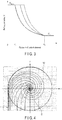
- the refractive index N is plotted with respect to the radius r.
- the area within the radius r c from the center O of the optical element 10 is called "core C.”
- the refractive index N o of the environment is 1.
- the refractive index N o of the environment is a constant which may take a different value depending on the environment.
- another example of the environment aside from air can be water.
- the refractive index N o of the environment is, for example, 1.33.
- the refractive index N of the continuous gradient index distribution area of the optical element 10 fulfills N ⁇ N 0 r 0 r for the area having the radius r of the optical element 10 of from r c to r o .
- the inner side of the core C containing the center O is provided with the first medium (for example, silicon).
- the inner side of the core C containing the center O has a refractive index that matches the maximum value N max of the refractive index N of the optical element 10.
- the radius of the contact area is r c and the maximum value of the radius r is r o .
- the core C (first medium) includes an area where the absolute value of the imaginary part K of the complex refractive index n is greater than zero.
- the optical element 10 includes an area which continuously attenuates the refractive index N as the radius r becomes larger, so that the refractive index N meets the equation (3) for the radius r from the center O.
- the optical element 10 matches the refractive index N o of the environment at the radius r o .
- the radius r o corresponds to, for example, the outer circumference of the optical element 10.
- Optical waves (which will be denoted by L) bend toward an area showing a higher refractive index N.
- the optical wave L incident on the optical element 10 having the distribution of the refractive index N that meets the equation (3) is always directed towards the center O of the optical element 10, regardless of its incident direction.
- each optical wave L here travels from the negative side to the positive side along the y-axis, and the optical wave L that intersects the x-axis in the negative domain is directed towards the center O with a higher refractive index N.
- This behavior is not limited to such a two-dimensional case as the xy-plane, but is also true in three-dimensional cases such as the xyz Cartesian coordinate system. Therefore, no matter what direction the optical wave L is incident upon the optical element 10, the optical wave L is directed towards the center O. Thus, when the optical wave L is incident upon the optical element 10, the optical wave L reaches the core C of the radius r c containing the center O.
- the refractive index N is continuous at the boundary (contact area) of the core C.
- the optical element 10 has no gap in the refractive index N at the boundary (contact area) of the core C. Therefore, there is no drastic change in the refractive index at the boundary (contact area) of the core C, which serves as a prevention against loss of light due to the Fresnel reflection in the optical element 10.
- the core C of the optical element 10 includes an area having an absolute value of the imaginary part K of the complex refractive index n that is greater than zero.
- the optical wave L is absorbed at this area in the core C of the optical element 10, where the absolute value of the imaginary part K of the complex refractive index n of the core C is greater than zero.
- the optical wave L entering the core C would exit the core C.
- the optical element 10 is adapted to collect the omnidirectional optical waves L to the core C and absorb the omnidirectional optical waves L. More specifically, by for example disposing an area sensor which converts the energy of the absorbed optical waves L into electricity, the omnidirectional information can be acquired as an image.
- an ordinary lens is not able to collect the omnidirectional optical waves L in the core C.
- an optical element 10 capable of collecting light omnidirectionally can be provided.
- the optical element 10 according to the first embodiment is of a spherical shape.
- the optical element 10 is not limited to a spherical shape.
- the shape of the optical element 10 of the present modification example is for example, a cylindrical shape.
- the shape of the optical element 10 may be another shape as long as the shape includes a cross section having a distribution of the refractive index N that meets the equation (3).
- any cross section intersecting the central axis of the cylinder is an xy-plane. In this case, similar to those shown in FIG. 4 , the incident optical wave L parallel to the xy-plane is directed to the center O along the xy-plane.
- an optical element 10 capable of collecting light omnidirectionally can be provided.
- FIG. 5 will be referred to for explaining a lighting apparatus 20 according to a second embodiment.
- the lighting apparatus 20 according to the second embodiment uses the optical element 10 explained in the first embodiment.
- the lighting apparatus 20 includes the spherical optical element 10, a fluorescent body 22, a transparent rod 24, and a light source 26.
- the rod 24 is for example, of a substantially cylindrical shape.
- the rod 24 supports the spherical optical element 10.
- the rod 24 and the spherical optical element 10 may be integrated. It is preferable if a refractive index of the rod 24 and the refractive index N of the optical element 10 at the radius r o (i.e., a refractive index of a boundary between the rod 24 and the optical element 10) match or substantially match each other.
- the light source 26 is disposed on, for example, the opposite side from the optical element 10.
- the light source 26 uses, for example, an LED (light-emitting diode).
- the light source 26 may for example be an LD (laser diode) or a laser.
- the light source 26 may be a tungsten filament as used in halogen lamps, etc.
- Various configurations or components may be used as the light source 26.
- a wavelength of the optical wave L emitted from the light source 26 may be, for example, 450 nm, and this will be called a first wavelength.
- the rod 24 transmits the optical wave L of the first wavelength emitted from the light source 26.
- a portion of the core C containing the center O explained in the first embodiment is constituted by the fluorescent body 22.
- the fluorescent body 22 is of a spherical shape.
- the fluorescent body 22 absorbs the first wavelength light and converts it to light of a second wavelength on the longer wavelength side.
- the second wavelength is 550 nm.
- the optical wave L of the first wavelength emitted from the light source 26 is incident on the transparent rod 24, and repeats total reflection in the rod 24 to reach the spherical optical element 10. A part of the optical wave L directly reaches the spherical optical element 10 without the total reflection in the rod 24.
- the optical wave L having reached the spherical optical element 10 is directed towards the core C of the optical element 10 as explained in the first embodiment.
- the optical wave L is directed toward the fluorescent body 22.
- the optical wave L of the first wavelength is absorbed by the fluorescent body 22.
- the optical wave L of the first wavelength absorbed by the fluorescent body 22 is emitted from the fluorescent body 22 as a optical wave having the second wavelength.
- Such optical waves are eventually emitted from the spherical optical element 10.
- the optical wave emitted from the fluorescent body 22 is an incoherent optical wave having a wide wavelength interval as compared to the optical wave of the first wavelength.
- the optical wave emitted from the fluorescent body 22 is dispersed in a wide light distribution. Such characteristics match the requirement of the lighting usage and are effective for the lighting usage.
- the optical wave L having the first wavelength emitted from the light source 26 is converted to the optical wave having the second wavelength at the fluorescent body 22 in the core C of the optical element 10, and emitted from the same.
- the optical element 10 endows the light with characteristics required for the lighting usage, such as a wide wavelength interval, incoherency, and a wide light distribution.
- the lighting apparatus 20 can realize characteristics required for the lighting usage, such as a wide wavelength interval, incoherency, and a wide light distribution.
- the lighting apparatus 20 can collect all of the light incident on the optical element 10 to the fluorescent body 22 in the core C.
- the optical wave L collected to the fluorescent body 22 in the core C is then emitted to the exterior with the wavelength changed.
- a lighting apparatus 20 giving an extremely high efficiency such as 100% is provided.
- the rod 24 is not essential.
- the light from the light source 26 may be directly incident on the optical element 10.
- FIG. 6 will be referred to for explaining a solar cell device 30 according to a third embodiment.
- the solar cell device 30 according to the third embodiment uses the optical element 10 explained in the first embodiment.
- the solar cell device 30 includes the spherical optical element 10 and a solar cell 32 as shown in FIG. 6 .
- the spherical optical element 10 is the same as the first embodiment except that the solar cell 32 is disposed in the core C. More specifically, the solar cell 32 is included as the medium (first medium) of the core C containing the center O. In other words, the solar cell 32 is in the medium (first medium) of the core C containing the center O.
- the solar cell 32 may be an energy-converting element used in photovoltaic generation or a reactor used in solar thermal power generation.
- the solar cell 32 may be a heat storage material.
- the solar cell 32 may be placed at a light collector for collecting light from the sun or a heat collector for collecting thermal energy converted from light from the sun.
- the optical element 10 according to the present embodiment can collect sunlight from every direction, as well as solar thermal energy based on sunlight, in the solar cell 32 (or the heat storage material) disposed in the core C. That is, the solar cell device 30 according to the present embodiment can collect sunlight from every direction in the solar cell 32 in the core C.
- the photovoltaic generation or solar thermal power generation can be efficiently performed without having to track the direction of the sun.
- the solar cell device 30 according to the present embodiment can collect all of the light incident on the optical element 10 in the core C. Therefore, all of the sunlight incident on the optical element 10 can be collected in the core C. In addition, all of the thermal energy obtained from the sunlight can be collected in the core C. Thus, according to the present embodiment, a solar cell device 30 giving an extremely high efficiency is provided.
Landscapes
- Physics & Mathematics (AREA)
- Optics & Photonics (AREA)
- Engineering & Computer Science (AREA)
- General Physics & Mathematics (AREA)
- General Engineering & Computer Science (AREA)
- Microelectronics & Electronic Packaging (AREA)
- Life Sciences & Earth Sciences (AREA)
- Sustainable Development (AREA)
- Toxicology (AREA)
- Health & Medical Sciences (AREA)
- Sustainable Energy (AREA)
- Thermal Sciences (AREA)
- Chemical & Material Sciences (AREA)
- Combustion & Propulsion (AREA)
- Mechanical Engineering (AREA)
- Non-Portable Lighting Devices Or Systems Thereof (AREA)
- Optical Elements Other Than Lenses (AREA)
- Photovoltaic Devices (AREA)
Abstract
Description
- Embodiments described herein relate generally to an optical element, a lighting apparatus and a solar cell device.
- In a conventional optical element such as a wide-angle lens, light rays can be collected from a wide viewing angle.
- In a normal wide-angle lens, it is difficult to collect light from a viewing angle of 360°, in other words, omnidirectionally.
-
-
FIG. 1 is a schematic view of a spherical optical element according to a first embodiment. -
FIG. 2 is a schematic view including a perspective view of the optical element shown inFIG. 1 cut in half at a plane including the center of the optical element, and an indication of a continuous gradient index distribution area which continuously and radially attenuates a refractive index from the center. -
FIG. 3 is a schematic graph showing a refractive index distribution between a refractive index of an area from the center to an outer edge of the core of the optical element shown inFIG. 1 , and a refractive index of a peripheral environment of the optical element. -
FIG. 4 is a schematic view showing a path of a optical wave in an xy-plane when the optical wave enters the optical element shown inFIG. 1 from a given direction. -
FIG. 5 is a schematic perspective view showing a lighting apparatus including the optical element shown inFIG. 1 , according to a second embodiment. -
FIG. 6 is a schematic view showing a solar cell device including the optical element shown inFIG. 1 , according to a third embodiment. - Hereinafter, embodiments will be described with reference to the accompanying drawings. The drawings are schematically or conceptually illustrated.
- The object to be achieved by the embodiments includes providing an omnidirectionally light-collecting optical element, a lighting apparatus including the optical element, and a solar cell device including the optical element.
- The optical element according to an embodiment includes a continuous gradient index distribution area which is configured to continuously attenuate a refractive index from a center of the optical element in a radial direction. The optical element includes a first medium at the center. The first medium includes an area where absolute value of imaginary part of a complex refractive index is greater than zero.
-
FIGS. 1 to 4 will be referred to for explaining anoptical element 10 according to a first embodiment. - The
optical element 10 according to the embodiment is formed from a medium (first medium) transparent to optical waves. As shown inFIG. 1 , theoptical element 10 according to the present embodiment is for example, of a spherical shape. Theoptical element 10 is not limited to such a shape and may adopt any shape as long as it is axisymmetrical. Thus, theoptical element 10 may be of a cylindrical shape. Theoptical element 10 may be a substantially-axisymmetric polygonal prism. Theoptical element 10 according to the present embodiment uses for example, a meta-lens. - Optical waves here includes visible light, x-rays, millimeter waves, or electromagnetic waves and are waves that include an electric field component and a magnetic field component. Transparent refers to a property of transmitting even a small amount of light and may involve absorption of optical waves. In one example, the optical wave is visible light and the medium is silicon. The complex refractive index n of the medium is given as:

- N is a real part and generally called a refractive index. K is an imaginary part and generally called an extinction coefficient.
-
FIG. 2 is a perspective view of the sphericaloptical element 10 according to the present embodiment, cut at a plane through the center O. The center O of theoptical element 10 of the present embodiment is set as the origin and Cartesian coordinates (x, y, z) are placed. InFIG. 2 , as one example, theoptical element 10 is cut in half at the plane of z=0. The refractive index N is shown by a color contour (gray scale contour) on the z=0 plane (xy-plane). The refractive index N of theoptical element 10 according to the present embodiment continuously changes from the center O towards an outer side. The refractive index N does not drastically decrease, but rather gradually decreases from the center O towards the outer side in the radial direction. Thus, theoptical element 10 includes a continuous gradient index distribution area which continuously attenuates the refractive index from the center O in a radial direction. In other words, the refractive index N of theoptical element 10 becomes higher towards the center O. - In
FIG. 3 , with the origin O as the center of theoptical element 10 according to the present embodiment, the refractive index N is plotted with respect to the radius r. The area within the radius rc from the center O of theoptical element 10 is called "core C." The distribution of the refractive index N shown inFIG. 3 , for the area having the radius r of from rc to ro, is represented as:
- According to the present embodiment, another example of the environment aside from air can be water. In such a case, the refractive index No of the environment is, for example, 1.33.
- m is a constant of 1 or more. In
FIG. 3 , a solid line shows when m is 1.0 and dashed lines show when m is 1.5 and when m is 2.0, respectively. The case where m is 1.5 is shown between the case where m is 1.0 and the case where m is 2.0. Thus, the refractive index N of the continuous gradient index distribution area of theoptical element 10 fulfills
optical element 10 of from rc to ro. Further, the maximum value Nmax of the refractive index of a contact area where the medium of the core C (first medium) contacts the continuous gradient index distribution area outside the core C is represented by:
optical element 10. In theoptical element 10, the radius of the contact area is rc and the maximum value of the radius r is ro. - The core C (first medium) includes an area where the absolute value of the imaginary part K of the complex refractive index n is greater than zero.
- As can be seen from the above, the
optical element 10 according to the present embodiment includes an area which continuously attenuates the refractive index N as the radius r becomes larger, so that the refractive index N meets the equation (3) for the radius r from the center O. Theoptical element 10 matches the refractive index No of the environment at the radius ro. The radius ro corresponds to, for example, the outer circumference of theoptical element 10. - The operation of the
optical element 10 according to the present embodiment will be explained. - Optical waves (which will be denoted by L) bend toward an area showing a higher refractive index N. According to the calculation based on a ray equation derived from Lagrangian optics, the optical wave L incident on the
optical element 10 having the distribution of the refractive index N that meets the equation (3) is always directed towards the center O of theoptical element 10, regardless of its incident direction. - For simplification of the explanation, as one example, an xy-plane where z=0 as shown in
FIG. 4 will be considered. Each optical wave L here travels from the negative side to the positive side along the y-axis, and the optical wave L that intersects the x-axis in the negative domain is directed towards the center O with a higher refractive index N. This behavior is not limited to such a two-dimensional case as the xy-plane, but is also true in three-dimensional cases such as the xyz Cartesian coordinate system. Therefore, no matter what direction the optical wave L is incident upon theoptical element 10, the optical wave L is directed towards the center O. Thus, when the optical wave L is incident upon theoptical element 10, the optical wave L reaches the core C of the radius rc containing the center O. - From the equation (4), the refractive index N is continuous at the boundary (contact area) of the core C. Thus, the
optical element 10 has no gap in the refractive index N at the boundary (contact area) of the core C. Therefore, there is no drastic change in the refractive index at the boundary (contact area) of the core C, which serves as a prevention against loss of light due to the Fresnel reflection in theoptical element 10. - The core C of the
optical element 10 includes an area having an absolute value of the imaginary part K of the complex refractive index n that is greater than zero. Thus, the optical wave L is absorbed at this area in the core C of theoptical element 10, where the absolute value of the imaginary part K of the complex refractive index n of the core C is greater than zero. On the other hand, if the absolute value of the imaginary part K is zero, the optical wave L entering the core C would exit the core C. In other words, theoptical element 10 is adapted to collect the omnidirectional optical waves L to the core C and absorb the omnidirectional optical waves L. More specifically, by for example disposing an area sensor which converts the energy of the absorbed optical waves L into electricity, the omnidirectional information can be acquired as an image. On the other hand, an ordinary lens is not able to collect the omnidirectional optical waves L in the core C. - According to the present embodiment, an
optical element 10 capable of collecting light omnidirectionally can be provided. - The
optical element 10 according to the first embodiment is of a spherical shape. Theoptical element 10 is not limited to a spherical shape. The shape of theoptical element 10 of the present modification example is for example, a cylindrical shape. The shape of theoptical element 10 may be another shape as long as the shape includes a cross section having a distribution of the refractive index N that meets the equation (3). By conforming the z-axis to the central axis of the cylinder, any cross section intersecting the central axis of the cylinder is an xy-plane. In this case, similar to those shown inFIG. 4 , the incident optical wave L parallel to the xy-plane is directed to the center O along the xy-plane. - According to the modification example, an
optical element 10 capable of collecting light omnidirectionally can be provided. - Next,
FIG. 5 will be referred to for explaining alighting apparatus 20 according to a second embodiment. Thelighting apparatus 20 according to the second embodiment uses theoptical element 10 explained in the first embodiment. - As shown in
FIG. 5 , thelighting apparatus 20 according to the present embodiment includes the sphericaloptical element 10, afluorescent body 22, atransparent rod 24, and alight source 26. - The
rod 24 is for example, of a substantially cylindrical shape. Therod 24 supports the sphericaloptical element 10. Therod 24 and the sphericaloptical element 10 may be integrated. It is preferable if a refractive index of therod 24 and the refractive index N of theoptical element 10 at the radius ro (i.e., a refractive index of a boundary between therod 24 and the optical element 10) match or substantially match each other. - In the
rod 24, thelight source 26 is disposed on, for example, the opposite side from theoptical element 10. Thelight source 26 uses, for example, an LED (light-emitting diode). Thelight source 26 may for example be an LD (laser diode) or a laser. Thelight source 26 may be a tungsten filament as used in halogen lamps, etc. Various configurations or components may be used as thelight source 26. A wavelength of the optical wave L emitted from thelight source 26 may be, for example, 450 nm, and this will be called a first wavelength. Therod 24 transmits the optical wave L of the first wavelength emitted from thelight source 26. - In the spherical
optical element 10, a portion of the core C containing the center O explained in the first embodiment is constituted by thefluorescent body 22. Thefluorescent body 22 is of a spherical shape. Thefluorescent body 22 absorbs the first wavelength light and converts it to light of a second wavelength on the longer wavelength side. For example, the second wavelength is 550 nm. - The operation of the
lighting apparatus 20 according to the present embodiment will be explained. - The optical wave L of the first wavelength emitted from the
light source 26 is incident on thetransparent rod 24, and repeats total reflection in therod 24 to reach the sphericaloptical element 10. A part of the optical wave L directly reaches the sphericaloptical element 10 without the total reflection in therod 24. - The optical wave L having reached the spherical
optical element 10 is directed towards the core C of theoptical element 10 as explained in the first embodiment. Thus, the optical wave L is directed toward thefluorescent body 22. The optical wave L of the first wavelength is absorbed by thefluorescent body 22. The optical wave L of the first wavelength absorbed by thefluorescent body 22 is emitted from thefluorescent body 22 as a optical wave having the second wavelength. Such optical waves are eventually emitted from the sphericaloptical element 10. - The optical wave emitted from the
fluorescent body 22 is an incoherent optical wave having a wide wavelength interval as compared to the optical wave of the first wavelength. The optical wave emitted from thefluorescent body 22 is dispersed in a wide light distribution. Such characteristics match the requirement of the lighting usage and are effective for the lighting usage. - With the above operation, the optical wave L having the first wavelength emitted from the
light source 26 is converted to the optical wave having the second wavelength at thefluorescent body 22 in the core C of theoptical element 10, and emitted from the same. In the course of this, theoptical element 10 endows the light with characteristics required for the lighting usage, such as a wide wavelength interval, incoherency, and a wide light distribution. Thus, thelighting apparatus 20 can realize characteristics required for the lighting usage, such as a wide wavelength interval, incoherency, and a wide light distribution. - The
lighting apparatus 20 according to the present embodiment can collect all of the light incident on theoptical element 10 to thefluorescent body 22 in the core C. The optical wave L collected to thefluorescent body 22 in the core C is then emitted to the exterior with the wavelength changed. Thus, according to the present embodiment, alighting apparatus 20 giving an extremely high efficiency such as 100% is provided. - Note that the
rod 24 is not essential. The light from thelight source 26 may be directly incident on theoptical element 10. - Next,
FIG. 6 will be referred to for explaining asolar cell device 30 according to a third embodiment. Thesolar cell device 30 according to the third embodiment uses theoptical element 10 explained in the first embodiment. - The
solar cell device 30 according to the present embodiment includes the sphericaloptical element 10 and asolar cell 32 as shown inFIG. 6 . - The spherical
optical element 10 is the same as the first embodiment except that thesolar cell 32 is disposed in the core C. More specifically, thesolar cell 32 is included as the medium (first medium) of the core C containing the center O. In other words, thesolar cell 32 is in the medium (first medium) of the core C containing the center O. Thesolar cell 32 may be an energy-converting element used in photovoltaic generation or a reactor used in solar thermal power generation. Thesolar cell 32 may be a heat storage material. Thesolar cell 32 may be placed at a light collector for collecting light from the sun or a heat collector for collecting thermal energy converted from light from the sun. - The
optical element 10 according to the present embodiment can collect sunlight from every direction, as well as solar thermal energy based on sunlight, in the solar cell 32 (or the heat storage material) disposed in the core C. That is, thesolar cell device 30 according to the present embodiment can collect sunlight from every direction in thesolar cell 32 in the core C. Thus, by using thesolar cell device 30 according to the present embodiment, the photovoltaic generation or solar thermal power generation can be efficiently performed without having to track the direction of the sun. - The
solar cell device 30 according to the present embodiment can collect all of the light incident on theoptical element 10 in the core C. Therefore, all of the sunlight incident on theoptical element 10 can be collected in the core C. In addition, all of the thermal energy obtained from the sunlight can be collected in the core C. Thus, according to the present embodiment, asolar cell device 30 giving an extremely high efficiency is provided. - According to the above embodiments, the following clauses can be obtained.
- Clause 1. An optical element comprising:
- a continuous gradient index distribution area which is configured to continuously attenuate gradient index from a center of the optical element in a radial direction; and
- a first medium at the center, the first medium including an area where absolute value of imaginary part of a complex refractive index is greater than zero.
- Clause 2. The optical element according to clause 1, wherein when a refractive index of the continuous gradient index distribution area is N, a radius from the center is r, a maximum value of the radius r is ro, and No is a constant,

- Clause 3. The optical element according to clause 1, wherein when a refractive index of a contact area between the first medium and the continuous gradient index distribution area is Nmax,
a radius of the contact area is rc,
a maximum value of a radius r of the optical element is ro, No is a constant, and m is a constant of 1 or more, and
- Clause 4. The optical element according to any one of clauses 1 to 3, wherein the first medium is a solar cell.
- Clause 5. A lighting apparatus comprising:
- the optical element according to any one of clauses 1 to 3; and
- a light source,
- wherein:
- the first medium is a fluorescent body,
- the light source is configured to emit light of a first wavelength, and
- the fluorescent body is configured to absorb the light of the first wavelength, convert the light of the first wavelength to light of a second wavelength longer than the first wavelength, and emit the light of the second wavelength.
- Clause 6. A solar cell device comprising;
the optical element according to any one of clauses 1 to 3; and
a solar cell which is in the first medium. - While certain arrangements have been described, these arrangements have been presented by way of example only, and are not intended to limit the scope of the inventions. Indeed, the apparatuses described herein may be embodied in a variety of other forms; furthermore, various omissions, substitutions and changes in the form of the apparatuses described herein may be made.
Claims (6)
- An optical element comprising:a continuous gradient index distribution area which is configured to continuously attenuate gradient index from a center of the optical element in a radial direction; anda first medium at the center, the first medium including an area where absolute value of imaginary part of a complex refractive index is greater than zero.
- The optical element according to claim 1, wherein when a refractive index of the continuous gradient index distribution area is N, a radius from the center is r, a maximum value of the radius r is ro, and No is a constant,

- The optical element according to claim 1, wherein when a refractive index of a contact area between the first medium and the continuous gradient index distribution area is Nmax,
a radius of the contact area is rc,
a maximum value of a radius r of the optical element is ro, No is a constant, and m is a constant of 1 or more, and
- The optical element according to any one of claims 1 to 3, wherein the first medium is a solar cell.
- A lighting apparatus comprising:the optical element according to any one of claims 1 to 3; anda light source,wherein:the first medium is a fluorescent body,the light source is configured to emit light of a first wavelength, andthe fluorescent body is configured to absorb the light of the first wavelength, convert the light of the first wavelength to light of a second wavelength longer than the first wavelength, and emit the light of the second wavelength.
- A solar cell device comprising;
the optical element according to any one of claims 1 to 3; and
a solar cell which is in the first medium.
Applications Claiming Priority (1)
| Application Number | Priority Date | Filing Date | Title |
|---|---|---|---|
| JP2019168953A JP7317646B2 (en) | 2019-09-18 | 2019-09-18 | Optical element, illumination device, and solar cell device |
Publications (2)
| Publication Number | Publication Date |
|---|---|
| EP3795923A1 true EP3795923A1 (en) | 2021-03-24 |
| EP3795923B1 EP3795923B1 (en) | 2024-11-06 |
Family
ID=69742729
Family Applications (1)
| Application Number | Title | Priority Date | Filing Date |
|---|---|---|---|
| EP20159739.0A Active EP3795923B1 (en) | 2019-09-18 | 2020-02-27 | Optical element, lighting apparatus, and solar cell device |
Country Status (3)
| Country | Link |
|---|---|
| US (1) | US11888438B2 (en) |
| EP (1) | EP3795923B1 (en) |
| JP (1) | JP7317646B2 (en) |
Citations (3)
| Publication number | Priority date | Publication date | Assignee | Title |
|---|---|---|---|---|
| JP2007214292A (en) * | 2006-02-08 | 2007-08-23 | Matsushita Electric Ind Co Ltd | Light receiving module and optical space transmission device |
| WO2011109096A1 (en) * | 2010-03-03 | 2011-09-09 | Cree, Inc | Led lamp incorporating remote phosphor with heat dissipation features |
| WO2012033840A2 (en) * | 2010-09-07 | 2012-03-15 | The Trustees Of Columbia University In The City Of New York | Spherical gradient index (grin) lenses and their uses in solar concentration |
Family Cites Families (11)
| Publication number | Priority date | Publication date | Assignee | Title |
|---|---|---|---|---|
| JP3396118B2 (en) | 1995-11-02 | 2003-04-14 | オリンパス光学工業株式会社 | Graded-index optical element and optical apparatus using the graded-index optical element |
| JPH10221558A (en) * | 1997-02-04 | 1998-08-21 | Mitsubishi Rayon Co Ltd | Optical transmitter, method of manufacturing the same, array, and method of using them |
| JP3002656B2 (en) * | 1997-09-16 | 2000-01-24 | 三菱レイヨン株式会社 | Manufacturing method of refractive index distribution type optical transmitter |
| KR101001547B1 (en) * | 2004-01-28 | 2010-12-17 | 삼성에스디아이 주식회사 | Fibrous solar cell and manufacturing method thereof |
| JP2005283771A (en) * | 2004-03-29 | 2005-10-13 | Fujikura Ltd | Gradient index rod lens, optical components |
| JP2009122146A (en) * | 2007-11-09 | 2009-06-04 | Panasonic Corp | Beam converter and light receiving device |
| EP2278369A1 (en) | 2008-05-13 | 2011-01-26 | Sumitomo Electric Industries, Ltd. | Photoelectric conversion unit |
| US9228761B2 (en) * | 2010-07-26 | 2016-01-05 | Purdue Research Foundation | Electromagnetic wave concentrator and absorber |
| KR20130024690A (en) * | 2011-08-29 | 2013-03-08 | 정재헌 | A light condensing lens |
| JP6045864B2 (en) * | 2012-09-20 | 2016-12-14 | 株式会社東芝 | LED lighting device |
| CN105009313B (en) | 2013-10-29 | 2017-04-12 | 飞利浦照明控股有限公司 | Phosphor-based lighting device and method for generating light output |
-
2019
- 2019-09-18 JP JP2019168953A patent/JP7317646B2/en active Active
-
2020
- 2020-02-27 EP EP20159739.0A patent/EP3795923B1/en active Active
- 2020-02-28 US US16/804,027 patent/US11888438B2/en active Active
Patent Citations (3)
| Publication number | Priority date | Publication date | Assignee | Title |
|---|---|---|---|---|
| JP2007214292A (en) * | 2006-02-08 | 2007-08-23 | Matsushita Electric Ind Co Ltd | Light receiving module and optical space transmission device |
| WO2011109096A1 (en) * | 2010-03-03 | 2011-09-09 | Cree, Inc | Led lamp incorporating remote phosphor with heat dissipation features |
| WO2012033840A2 (en) * | 2010-09-07 | 2012-03-15 | The Trustees Of Columbia University In The City Of New York | Spherical gradient index (grin) lenses and their uses in solar concentration |
Non-Patent Citations (2)
| Title |
|---|
| HAIBING CHEN ET AL: "Modified Luneburg Lens Based on Metamaterials", INTERNATIONAL JOURNAL OF ANTENNAS AND PROPAGATION, vol. 2015, 1 January 2015 (2015-01-01), pages 1 - 6, XP055736130, ISSN: 1687-5869, DOI: 10.1155/2015/902634 * |
| JEFFREY M. GORDON: "Spherical gradient-index lenses as perfect imaging and maximum power transfer devices", APPLIED OPTICS, vol. 39, no. 22, 1 August 2000 (2000-08-01), US, pages 3825, XP055736106, ISSN: 0003-6935, DOI: 10.1364/AO.39.003825 * |
Also Published As
| Publication number | Publication date |
|---|---|
| JP7317646B2 (en) | 2023-07-31 |
| US20210083620A1 (en) | 2021-03-18 |
| US11888438B2 (en) | 2024-01-30 |
| EP3795923B1 (en) | 2024-11-06 |
| JP2021047267A (en) | 2021-03-25 |
Similar Documents
| Publication | Publication Date | Title |
|---|---|---|
| JP4290900B2 (en) | Light source device | |
| EP3373049B1 (en) | Projection light source device | |
| WO2006102317A2 (en) | Multi-junction solar cells with an aplanatic imaging system | |
| US11855705B2 (en) | Distributed optical resonator with thin receiver unit | |
| US8355214B2 (en) | Light collection apparatus, system and method | |
| KR101791130B1 (en) | Solar cell module | |
| US7102824B2 (en) | Optical element for efficient sensing at large angles of incidence | |
| EP2133928A2 (en) | Reflective Light Concentrator | |
| US8633377B2 (en) | Light concentration apparatus, systems and methods | |
| EP3795923B1 (en) | Optical element, lighting apparatus, and solar cell device | |
| US20060274439A1 (en) | Optical system using tailored imaging designs | |
| CN215641912U (en) | Diaphragm and laser | |
| US11456396B2 (en) | Photoelectric conversion device for solar photovoltaic generation | |
| CN215641913U (en) | Diaphragm and laser | |
| WO2002007228A1 (en) | Light emitting diode with lens | |
| US8684545B2 (en) | Light concentration apparatus, systems and methods | |
| KR101480565B1 (en) | Photovoltaic device | |
| CN206515548U (en) | Off-axis four-mirror optical imaging system in the deep ultraviolet spectrum | |
| US20120111397A1 (en) | Kohler homogenizer for solar concentrator | |
| JP2014045133A (en) | Concentrating solar cell module | |
| JP2018018981A (en) | Fluorescent light confinement structure of sunlight excitation laser device | |
| Evans | Principles Of Stray Light Suppression And Conceptual Application To The Design Of The Diffuse Infrared Background Experiment For NASA's Cosmic Background Explorer. | |
| Nakar et al. | Near-field tailored imaging optics for coupling ultra-bright light sources into optical fibers |
Legal Events
| Date | Code | Title | Description |
|---|---|---|---|
| PUAI | Public reference made under article 153(3) epc to a published international application that has entered the european phase |
Free format text: ORIGINAL CODE: 0009012 |
|
| STAA | Information on the status of an ep patent application or granted ep patent |
Free format text: STATUS: REQUEST FOR EXAMINATION WAS MADE |
|
| 17P | Request for examination filed |
Effective date: 20200227 |
|
| AK | Designated contracting states |
Kind code of ref document: A1 Designated state(s): AL AT BE BG CH CY CZ DE DK EE ES FI FR GB GR HR HU IE IS IT LI LT LU LV MC MK MT NL NO PL PT RO RS SE SI SK SM TR |
|
| AX | Request for extension of the european patent |
Extension state: BA ME |
|
| STAA | Information on the status of an ep patent application or granted ep patent |
Free format text: STATUS: EXAMINATION IS IN PROGRESS |
|
| 17Q | First examination report despatched |
Effective date: 20230222 |
|
| GRAP | Despatch of communication of intention to grant a patent |
Free format text: ORIGINAL CODE: EPIDOSNIGR1 |
|
| STAA | Information on the status of an ep patent application or granted ep patent |
Free format text: STATUS: GRANT OF PATENT IS INTENDED |
|
| INTG | Intention to grant announced |
Effective date: 20240726 |
|
| GRAS | Grant fee paid |
Free format text: ORIGINAL CODE: EPIDOSNIGR3 |
|
| GRAA | (expected) grant |
Free format text: ORIGINAL CODE: 0009210 |
|
| STAA | Information on the status of an ep patent application or granted ep patent |
Free format text: STATUS: THE PATENT HAS BEEN GRANTED |
|
| AK | Designated contracting states |
Kind code of ref document: B1 Designated state(s): AL AT BE BG CH CY CZ DE DK EE ES FI FR GB GR HR HU IE IS IT LI LT LU LV MC MK MT NL NO PL PT RO RS SE SI SK SM TR |
|
| REG | Reference to a national code |
Ref country code: GB Ref legal event code: FG4D |
|
| REG | Reference to a national code |
Ref country code: CH Ref legal event code: EP |
|
| REG | Reference to a national code |
Ref country code: DE Ref legal event code: R096 Ref document number: 602020040646 Country of ref document: DE |
|
| REG | Reference to a national code |
Ref country code: IE Ref legal event code: FG4D |
|
| REG | Reference to a national code |
Ref country code: LT Ref legal event code: MG9D |
|
| REG | Reference to a national code |
Ref country code: NL Ref legal event code: MP Effective date: 20241106 |
|
| PG25 | Lapsed in a contracting state [announced via postgrant information from national office to epo] |
Ref country code: HR Free format text: LAPSE BECAUSE OF FAILURE TO SUBMIT A TRANSLATION OF THE DESCRIPTION OR TO PAY THE FEE WITHIN THE PRESCRIBED TIME-LIMIT Effective date: 20241106 Ref country code: PT Free format text: LAPSE BECAUSE OF FAILURE TO SUBMIT A TRANSLATION OF THE DESCRIPTION OR TO PAY THE FEE WITHIN THE PRESCRIBED TIME-LIMIT Effective date: 20250306 Ref country code: IS Free format text: LAPSE BECAUSE OF FAILURE TO SUBMIT A TRANSLATION OF THE DESCRIPTION OR TO PAY THE FEE WITHIN THE PRESCRIBED TIME-LIMIT Effective date: 20250306 |
|
| PG25 | Lapsed in a contracting state [announced via postgrant information from national office to epo] |
Ref country code: FI Free format text: LAPSE BECAUSE OF FAILURE TO SUBMIT A TRANSLATION OF THE DESCRIPTION OR TO PAY THE FEE WITHIN THE PRESCRIBED TIME-LIMIT Effective date: 20241106 Ref country code: NL Free format text: LAPSE BECAUSE OF FAILURE TO SUBMIT A TRANSLATION OF THE DESCRIPTION OR TO PAY THE FEE WITHIN THE PRESCRIBED TIME-LIMIT Effective date: 20241106 |
|
| REG | Reference to a national code |
Ref country code: AT Ref legal event code: MK05 Ref document number: 1739724 Country of ref document: AT Kind code of ref document: T Effective date: 20241106 |
|
| PG25 | Lapsed in a contracting state [announced via postgrant information from national office to epo] |
Ref country code: BG Free format text: LAPSE BECAUSE OF FAILURE TO SUBMIT A TRANSLATION OF THE DESCRIPTION OR TO PAY THE FEE WITHIN THE PRESCRIBED TIME-LIMIT Effective date: 20241106 |
|
| PG25 | Lapsed in a contracting state [announced via postgrant information from national office to epo] |
Ref country code: ES Free format text: LAPSE BECAUSE OF FAILURE TO SUBMIT A TRANSLATION OF THE DESCRIPTION OR TO PAY THE FEE WITHIN THE PRESCRIBED TIME-LIMIT Effective date: 20241106 |
|
| PG25 | Lapsed in a contracting state [announced via postgrant information from national office to epo] |
Ref country code: NO Free format text: LAPSE BECAUSE OF FAILURE TO SUBMIT A TRANSLATION OF THE DESCRIPTION OR TO PAY THE FEE WITHIN THE PRESCRIBED TIME-LIMIT Effective date: 20250206 |
|
| PG25 | Lapsed in a contracting state [announced via postgrant information from national office to epo] |
Ref country code: GR Free format text: LAPSE BECAUSE OF FAILURE TO SUBMIT A TRANSLATION OF THE DESCRIPTION OR TO PAY THE FEE WITHIN THE PRESCRIBED TIME-LIMIT Effective date: 20250207 Ref country code: LV Free format text: LAPSE BECAUSE OF FAILURE TO SUBMIT A TRANSLATION OF THE DESCRIPTION OR TO PAY THE FEE WITHIN THE PRESCRIBED TIME-LIMIT Effective date: 20241106 Ref country code: AT Free format text: LAPSE BECAUSE OF FAILURE TO SUBMIT A TRANSLATION OF THE DESCRIPTION OR TO PAY THE FEE WITHIN THE PRESCRIBED TIME-LIMIT Effective date: 20241106 |
|
| PG25 | Lapsed in a contracting state [announced via postgrant information from national office to epo] |
Ref country code: PL Free format text: LAPSE BECAUSE OF FAILURE TO SUBMIT A TRANSLATION OF THE DESCRIPTION OR TO PAY THE FEE WITHIN THE PRESCRIBED TIME-LIMIT Effective date: 20241106 |
|
| PG25 | Lapsed in a contracting state [announced via postgrant information from national office to epo] |
Ref country code: RS Free format text: LAPSE BECAUSE OF FAILURE TO SUBMIT A TRANSLATION OF THE DESCRIPTION OR TO PAY THE FEE WITHIN THE PRESCRIBED TIME-LIMIT Effective date: 20250206 |
|
| PG25 | Lapsed in a contracting state [announced via postgrant information from national office to epo] |
Ref country code: SM Free format text: LAPSE BECAUSE OF FAILURE TO SUBMIT A TRANSLATION OF THE DESCRIPTION OR TO PAY THE FEE WITHIN THE PRESCRIBED TIME-LIMIT Effective date: 20241106 |
|
| PG25 | Lapsed in a contracting state [announced via postgrant information from national office to epo] |
Ref country code: DK Free format text: LAPSE BECAUSE OF FAILURE TO SUBMIT A TRANSLATION OF THE DESCRIPTION OR TO PAY THE FEE WITHIN THE PRESCRIBED TIME-LIMIT Effective date: 20241106 |
|
| PG25 | Lapsed in a contracting state [announced via postgrant information from national office to epo] |
Ref country code: EE Free format text: LAPSE BECAUSE OF FAILURE TO SUBMIT A TRANSLATION OF THE DESCRIPTION OR TO PAY THE FEE WITHIN THE PRESCRIBED TIME-LIMIT Effective date: 20241106 |
|
| PG25 | Lapsed in a contracting state [announced via postgrant information from national office to epo] |
Ref country code: RO Free format text: LAPSE BECAUSE OF FAILURE TO SUBMIT A TRANSLATION OF THE DESCRIPTION OR TO PAY THE FEE WITHIN THE PRESCRIBED TIME-LIMIT Effective date: 20241106 |
|
| PG25 | Lapsed in a contracting state [announced via postgrant information from national office to epo] |
Ref country code: SK Free format text: LAPSE BECAUSE OF FAILURE TO SUBMIT A TRANSLATION OF THE DESCRIPTION OR TO PAY THE FEE WITHIN THE PRESCRIBED TIME-LIMIT Effective date: 20241106 |
|
| PG25 | Lapsed in a contracting state [announced via postgrant information from national office to epo] |
Ref country code: CZ Free format text: LAPSE BECAUSE OF FAILURE TO SUBMIT A TRANSLATION OF THE DESCRIPTION OR TO PAY THE FEE WITHIN THE PRESCRIBED TIME-LIMIT Effective date: 20241106 |
|
| PG25 | Lapsed in a contracting state [announced via postgrant information from national office to epo] |
Ref country code: IT Free format text: LAPSE BECAUSE OF FAILURE TO SUBMIT A TRANSLATION OF THE DESCRIPTION OR TO PAY THE FEE WITHIN THE PRESCRIBED TIME-LIMIT Effective date: 20241106 |
|
| REG | Reference to a national code |
Ref country code: DE Ref legal event code: R097 Ref document number: 602020040646 Country of ref document: DE |
|
| PG25 | Lapsed in a contracting state [announced via postgrant information from national office to epo] |
Ref country code: SE Free format text: LAPSE BECAUSE OF FAILURE TO SUBMIT A TRANSLATION OF THE DESCRIPTION OR TO PAY THE FEE WITHIN THE PRESCRIBED TIME-LIMIT Effective date: 20241106 |
|
| PLBE | No opposition filed within time limit |
Free format text: ORIGINAL CODE: 0009261 |
|
| STAA | Information on the status of an ep patent application or granted ep patent |
Free format text: STATUS: NO OPPOSITION FILED WITHIN TIME LIMIT |
|
| PG25 | Lapsed in a contracting state [announced via postgrant information from national office to epo] |
Ref country code: MC Free format text: LAPSE BECAUSE OF FAILURE TO SUBMIT A TRANSLATION OF THE DESCRIPTION OR TO PAY THE FEE WITHIN THE PRESCRIBED TIME-LIMIT Effective date: 20241106 |
|
| REG | Reference to a national code |
Ref country code: CH Ref legal event code: PL |
|
| 26N | No opposition filed |
Effective date: 20250807 |
|
| PG25 | Lapsed in a contracting state [announced via postgrant information from national office to epo] |
Ref country code: LU Free format text: LAPSE BECAUSE OF NON-PAYMENT OF DUE FEES Effective date: 20250227 |
|
| PG25 | Lapsed in a contracting state [announced via postgrant information from national office to epo] |
Ref country code: CH Free format text: LAPSE BECAUSE OF NON-PAYMENT OF DUE FEES Effective date: 20250228 |
|
| GBPC | Gb: european patent ceased through non-payment of renewal fee |
Effective date: 20250227 |
|
| REG | Reference to a national code |
Ref country code: BE Ref legal event code: MM Effective date: 20250228 |
|
| PG25 | Lapsed in a contracting state [announced via postgrant information from national office to epo] |
Ref country code: GB Free format text: LAPSE BECAUSE OF NON-PAYMENT OF DUE FEES Effective date: 20250227 |
|
| PG25 | Lapsed in a contracting state [announced via postgrant information from national office to epo] |
Ref country code: FR Free format text: LAPSE BECAUSE OF NON-PAYMENT OF DUE FEES Effective date: 20250228 |
|
| PG25 | Lapsed in a contracting state [announced via postgrant information from national office to epo] |
Ref country code: BE Free format text: LAPSE BECAUSE OF NON-PAYMENT OF DUE FEES Effective date: 20250228 |
|
| PG25 | Lapsed in a contracting state [announced via postgrant information from national office to epo] |
Ref country code: IE Free format text: LAPSE BECAUSE OF NON-PAYMENT OF DUE FEES Effective date: 20250227 |
|
| PGFP | Annual fee paid to national office [announced via postgrant information from national office to epo] |
Ref country code: DE Payment date: 20260102 Year of fee payment: 7 |