EP3794362B1 - Metalldetektor - Google Patents
Metalldetektor Download PDFInfo
- Publication number
- EP3794362B1 EP3794362B1 EP19803062.9A EP19803062A EP3794362B1 EP 3794362 B1 EP3794362 B1 EP 3794362B1 EP 19803062 A EP19803062 A EP 19803062A EP 3794362 B1 EP3794362 B1 EP 3794362B1
- Authority
- EP
- European Patent Office
- Prior art keywords
- signal
- output
- vector
- resistive component
- notch module
- Prior art date
- Legal status (The legal status is an assumption and is not a legal conclusion. Google has not performed a legal analysis and makes no representation as to the accuracy of the status listed.)
- Active
Links
Images


Classifications
-
- G—PHYSICS
- G01—MEASURING; TESTING
- G01V—GEOPHYSICS; GRAVITATIONAL MEASUREMENTS; DETECTING MASSES OR OBJECTS; TAGS
- G01V3/00—Electric or magnetic prospecting or detecting; Measuring magnetic field characteristics of the earth, e.g. declination, deviation
- G01V3/15—Electric or magnetic prospecting or detecting; Measuring magnetic field characteristics of the earth, e.g. declination, deviation specially adapted for use during transport, e.g. by a person, vehicle or boat
- G01V3/165—Electric or magnetic prospecting or detecting; Measuring magnetic field characteristics of the earth, e.g. declination, deviation specially adapted for use during transport, e.g. by a person, vehicle or boat operating with magnetic or electric fields produced or modified by the object or by the detecting device
-
- G—PHYSICS
- G01—MEASURING; TESTING
- G01V—GEOPHYSICS; GRAVITATIONAL MEASUREMENTS; DETECTING MASSES OR OBJECTS; TAGS
- G01V3/00—Electric or magnetic prospecting or detecting; Measuring magnetic field characteristics of the earth, e.g. declination, deviation
- G01V3/08—Electric or magnetic prospecting or detecting; Measuring magnetic field characteristics of the earth, e.g. declination, deviation operating with magnetic or electric fields produced or modified by objects or geological structures or by detecting devices
- G01V3/10—Electric or magnetic prospecting or detecting; Measuring magnetic field characteristics of the earth, e.g. declination, deviation operating with magnetic or electric fields produced or modified by objects or geological structures or by detecting devices using induction coils
-
- G—PHYSICS
- G01—MEASURING; TESTING
- G01V—GEOPHYSICS; GRAVITATIONAL MEASUREMENTS; DETECTING MASSES OR OBJECTS; TAGS
- G01V3/00—Electric or magnetic prospecting or detecting; Measuring magnetic field characteristics of the earth, e.g. declination, deviation
- G01V3/38—Processing data, e.g. for analysis, for interpretation, for correction
Definitions
- the present invention relates to metal detectors and, more particularly, to a mixed domain metal detector that applies inverse transfer functions to improve ability to detect desired targets.
- Metal detectors exist in a variety of forms and are designed to detect desirable metal objects, herein referred to as targets. These include hand-held battery operated metal detectors, vehicle mounted metal detectors, walk through metal detectors and so on.
- a typical metal detector has a search sensor composed of a transmit coil and a receive coil. In some metal detectors a single coil acts as both the transmit coil and the receive coil.
- the transmit coil generates a time-varying magnetic field signal which excites various targets such as coins, mines, artifacts and so on that are buried in mediums such as soil, salt water beaches, clay, black sand and so on.
- targets In response to a transmitted magnetic field signal, targets generate secondary magnetic fields. Further, a medium that is conductive, magnetic, or conductive and magnetic will also generate its own secondary magnetic field in response to the transmitted magnetic field signal.
- the physics is well known.
- the receive coil picks up a response signal that is a function of the sum of the secondary magnetic fields from the target and the medium. Signal processing on the response signal is performed to produce an alert output to an operator to indicate when a desirable target is detected.
- the patent application document US2007/0046288 discloses, for example, a detector of metal target objects with a transmitter coil driven by a current pulse, a receiver coil and a compensation circuit formed by a compensating coil that determines a signal generated at the transmitter coil and provides a correction voltage level to a pre-amplifier of the signal of the receiver coil, to generate a signal compensated for the voltage generated by direct coupling between the transmitter and receiver coils.
- the metal detector further comprises a resistive component demodulator that outputs a resistive component of the compensated signal and a reactive component demodulator that outputs a reactive component of the compensated signal.
- the patent application document US2012/0025815 discloses a detector of metal target objects, which comprises a transmitter coil and a receiver coil, a notch or/and a low-pass filter, a synchronous demodulator of resistive and reactive components of a received signal.
- the notch or/and a low-pass filter reduces environmental magnetic noise from an amplified received signal by removing higher harmonics before the signal is input to the synchronous demodulator.
- the parameters of the response signal are affected by a variety of factors including target and medium transfer functions, distance from the search sensor, parameters of search sensor coils, generated transmit magnetic field, and frequency of transmit signal and so on.
- the parameters of search sensor coils include, for example dimensions of the coils, number of turns, coil DC resistance and so on.
- a target's electromagnetic behavior can be modeled with a target transfer function which is represented as a sum of a target magnetic component transfer function and a target resistive component transfer function.
- a medium electromagnetic behavior can be modeled with a medium transfer function which is represented as a sum of a medium magnetic component transfer function and a medium resistive component transfer function.
- the response signal from a target will be a sum of target magnetic and target resistive components.
- the medium response signal will be a sum of medium magnetic and medium resistive components.
- the medium is uniform, there is a correlation between the resistive and the magnetic components of the medium response signal. This makes it relatively easy to compensate or remove the undesired medium signal.
- the medium is not uniform, there may be little or no correlation between the resistive and magnetic components of the medium response signal. If the undesirable medium signal is not removed or compensated for, the performance of the metal detector may suffer by producing false positive outputs to the operator, reducing the detectable range of a desired target, completely masking a secondary target signal or resulting in incorrect target
- Figure 1 shows a simplified block diagram for a metal detector.
- the metal detector uses a medium resistive component inverse transfer function to compensate for the medium resistive component and uses preset target resistive component inverse transfer functions to properly identify the target.
- the metal detector signal processing applies the preset medium resistive component inverse transfer function (1/ W mr ) to the signal received by the metal detector's receiver and processes it in a time domain manner to compensate and remove the medium's resistive component from the signal received by the metal detector's receiver.
- the response signal is demodulated with vector resistive, denoted R, and vector reactive, denoted X, quadrature synchronous demodulators to be analyzed in the frequency domain and to remove the medium's magnetic component.
- the R demodulator is most sensitive to the purely resistive secondary field and the X demodulator is most sensitive to the purely reactive secondary field components for the demodulator's reference signal frequency.
- the phase reference signals frequency of the R and X demodulators can be the fundamental or harmonic frequency of the metal detector excitation signal as required to analyze the response signal vector at that frequency in the frequency domain.
- Figure 1 shows that the metal detector includes a search sensor 5 that has a transmitter component composed of a transmit coil 3 and a receiver component composed of a receive coil 6.
- transmit coil 3 is modeled as an effective transmit coil inductive component 2 in series with a resistive component 1.
- Resistive component 1 is the sum of the transmit coil DC resistance, search sensor cable DC resistance and a voltage power amplifier 20 output resistance.
- a typical range for inductance (L tc ) of effective transmit coil inductive (L tc ) component 2 is 200 Microhenry ( ⁇ H) to 1000 ⁇ H.
- a typical range for resistance (R tc ) of resistive component 1 is 0.5 Ohms to 2.0 Ohms.
- Voltage power amplifier 20, connected to transmit coil 3, generates a voltage signal that results in an excitation signal 100 that emanates from transmit coil 3 to produce an alternating magnet field 302.
- Alternating magnetic field 302 induces voltage in a target 301 and induces voltage in a medium 300.
- the induced voltage in target 301 and medium 300 generate a secondary target magnetic field 303 and a secondary medium magnetic field 304.
- a timing generator 30 presents a bipolar square waveform system excitation signal 126 to voltage power amplifier 20 that voltage power amplifier 20 amplifies to produce excitation signal 100.
- Figure 1 shows a target 301 within medium 300.
- Figure 2 shows an example waveform 200 of bipolar square waveform system excitation signal 126.
- Waveform 200 has a period with duration 201.
- Figure 3 shows an example waveform 202 of excitation signal 100.
- Waveform 202 also has a period with duration 201.
- the waveform of excitation signal can vary from what is shown in Figure 3 .
- excitation signal 100 can have, a square waveform, a bipolar square waveform, a rectangular waveform, a multilevel rectangular waveform or another type of waveform.
- a receive coil 6 has an inductive component 4.
- the induced voltage, response signal 305, in receive coil 6 inductive component 4 is a product of the alternating magnetic field generated by transmit coil 3. This is a sum of the secondary target magnetic field 303 and the secondary medium magnetic field 304.
- a pre-amplifier 41 amplifies response signal 305 and forwards an amplified signal 1010 to compensation circuitry 42.
- Compensation circuitry 42 includes transmit coil transfer function compensation electronics that produce a detected signal 101.
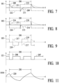
- Figure 11 shows an example waveform 220 for amplified signal 1010.
- Figure 7 shows waveform examples for detected signal 101 illustrating metal detector response to secondary target magnetic field 303 and secondary medium magnetic field 304 at compensation circuitry 42 output.
- a waveform 211 represents the response from the medium resistive component (M mr ).
- a waveform 212 represents the response from the medium magnetic component (M mm ).
- Waveform 209 represents the non-ferrous target response.
- the target is non-ferrous (target magnetic component is zero).
- a metal detector module 8 includes a notch module 7.
- Notch module 7 is used to filter out the medium resistive component from detected signal 101.
- Notch module 7 includes medium resistive component compensation electronics 51, with a transfer function the same as the medium's resistive component inverse transfer function and adjustable timing constant, and a gate 52.
- a regulator 54 is used to adjust the medium resistive component compensation circuit 51 preset timing constant (T mrc ) to the medium resistive component transfer function timing constant.
- Medium resistive component compensation circuit 51 generates an output signal 102.
- Figure 8 shows example waveforms for output signal 102.
- the waveforms includes target waveform 216 that represents the secondary magnetic field from the target, includes medium resistive component waveform 215 that represents the resistive component (M mr ) for the medium and includes medium magnetic component waveform 218 that represents the magnetic component (M mm ) for the medium.
- Timing generator 30 generates a gate control signal 120 to control gate 52 in order to produce gate output signal 103.
- gate control signal 120 is high, control gate 52 is open and output signal 102 passes through control gate 52.
- gate control signal 120 is Low, output signal 102 is blocked.
- a noise rejection low pass filter 53 filters gate output signal 103.
- noise rejection low pass filter 53 has a cutoff frequency between 60 kHz and 70 kHz.
- FIG. 6 shows an example waveform 205 for digital control signal 120.
- each falling edge is aligned with a transition (either a falling edge or a rising edge) of waveform 200 for bipolar square waveform system excitation signal 126, shown in Figure 2 .
- a falling edge is followed by a rising edge after digital control signal time width 206.
- Figure 9 shows sample waveforms for gate output signal 103.
- the waveforms includes target waveform 217 that represents the secondary magnetic field from the target and includes medium magnetic component waveform 219 that represents the magnetic component (M mm ) for the medium.
- Metal detector module 8 also includes quadrature signal 103 vector resistive (R) and reactive (X) components synchronous demodulators consisting of a vector resistive (R) component demodulator 61 and a vector reactive (X) component demodulator 62.
- Noise rejection low pass filter 53 forwards the filtered signal to signal's vector resistive component demodulator 61 and a signal's vector reactive component demodulator 62.
- Demodulator 61 and demodulator 62 each include a low pass filter (LPF) with, for example, a 15Hz to 20Hz cutoff frequency. The low pass filters within demodulator 61 and demodulator 62 filter all undesirable products from the demodulation process.
- LPF low pass filter
- Timing generator 30 provides an in-phase (with signal 126 with waveform 200) reference signal 124 with waveform 203 received on an input 129 of demodulator 61 and a quadrature to signal 126 with waveform 200 reference signal 125 with waveform 204 received on an input 130 of demodulator 62.
- Demodulator 61 produces an output signal 127 that is proportional to the vector resistive component of gate output signal 103, for gate output signal 103 having a fundamental frequency with a period duration 201.
- Demodulator 62 produces an output signal 128 that is proportional to the vector reactive component for gate output signal 103 fundamental frequency with a period duration 201.
- Figure 4 shows an example waveform 203 of in-phase reference signal 124.
- Figure 5 shows an example waveform 204 quadrature reference signal 125. Both, waveform 202 and waveform 203 have a period with duration 201.
- a multi-channel analog-to-digital converter (ADC) 70 digitizes output signals from demodulator 61 and demodulator 62 to provide digitized signals for further signal processing by a digital signal processor (DSP) and control module 80.
- DSP digital signal processor
- An indicator module 90 connected to DSP and control module 80, produces a desirable metal detected signal to the operator when a desired target is detected.
- timing generator 30 can be incorporated into DSP and control module 80.
- introducing multiple modules with transfer functions with preset timing constants and analyzing the modules composite signals increases resolution used in determination of a timing constant (Tt) for the target resistive component transfer function and allows identification of the target.
- Tt timing constant
- a metal detector module 8a and a metal detector module 8n which represent any number of multiple modules 8a...8n with the internal target resistive component notch modules 7a...7n.
- the modules 7a..7n target resistive component compensation circuits 51a...51n transfer function is the target resistive component inversed transfer function and different preset timing constants T51a...T51n. Analyzing the composite signals S7a... S7n product of the module's 8a...8n outputs, allows determination of the timing constant (Tt) for the target and the target identification.
- Figure 1 shows gate output signal 103 providing input to target resistive component compensation circuit 51a of a notch module 7a within metal detector module 8a and providing input to target resistive component transfer function compensation circuit 51n of a notch module 7n within metal detector module 8n.
- Notch module 7a is used to filter out target's resistive component with a transfer function timing constant equal to target resistive component compensation circuit 51a transfer function preset timing constant, still present in gate output signal 103.
- notch module 7n is used to filter out another target's resistive component with a transfer function timing constant equal to the target resistive component compensation circuit 51n transfer function preset timing constant, still present in gate output signal 103.
- Timing generator 30 generates a digital gate control signal 121 to control a gate 52a in order to produce gate output signal 103a and to control a gate 52n in order to produce gate output signal 103n.
- gate control signal 121 When gate control signal 121 is high, the gates are open and signals pass through the gates. When gate control signal 121 is Low the signals are blocked.
- Figure 10 shows an example waveform 207 for digital control signal 121 used to control gates 52a...52n. Every falling edge for waveform 207 for digital control signal 121 is aligned with a corresponding falling edge of waveform 205 for digital control signal 120, shown in Figure 6 . In waveform 207, a falling edge is followed by a rising edge after a time duration 208 where time duration 208 greater than digital control signal time width 206 of waveform 205.
- a noise reduction low pass filter (LPF) 53a input receives gate output signal 103a from gate 52a output.
- LPF 53a has a cutoff frequency between 60 kHz and 70 kHz.
- An output of LPF 53a is used to drive quadrature, Ra and Xa, synchronous demodulators 61a and 62a.
- Timing generator 30 provides in-phase reference signal 124 received on an input 129a of demodulator 61a and quadrature reference signal 125 received on an input 130a of demodulator 62a.
- Demodulator 61a produces an output signal 127a that is proportional to signal 103a vector resistive component of gate output signal 103a.
- Demodulator 62a produces an output signal 128a that is proportional to signal 103a vector reactive component.
- FIG. 1 shows the timing generator 30 providing fundamental transmit signal frequency quadrature reference signal pair 124 and 125 to demodulator 61a and demodulator 62a
- Demodulators 61a and 62a include a low pass filter (LPF) with, for example, a 15Hz to 20Hz cutoff frequency.
- LPF low pass filter
- Demodulators 61a and 62a LPF filter all undesirable products from the demodulation process.
- transmit signal harmonics frequency quadrature reference signal pairs being generated by timing generator 30 are represented in Figure 1 by transmit signal harmonics frequency quadrature reference signal pair 124a and 125a, and by transmit signal harmonics frequency quadrature reference signal pair 124n and 125n.
- a noise reduction LPF 53n input receives gate output signal 103n from gate 52n output.
- An output of LPF 53n is used to drive quadrature, Rn and Xn, synchronous demodulators 61n and 62n.
- Demodulators 61n and 62n include a low pass filter (LPF) with, for example, a 15Hz to 20Hz cutoff frequency. Demodulators 61n and 62n LPF filter all undesirable products from the demodulation process.
- Timing generator 30 provides an in-phase reference signal 124n received on an input 129n of demodulator 61n and a quadrature reference signal 125n received on an input 130n of demodulator 62n.
- Demodulator 61n produces an output signal 127n that is proportional to the vector resistive component of gate output signal 103n.
- Demodulator 62n produces an output signal 128n that is proportional to the vector reactive component.
- Figure 1 shows the timing generator 30 providing fundamental transmit signal frequency quadrature reference signal pair 124 and 125 to demodulator 61n and demodulator 62n, instead one of the transmit signal harmonics frequency quadrature reference signal pairs may be supplied. These are represented in Figure 1 by transmit signal harmonics frequency quadrature reference signal pair 124a and 125a, and by transmit signal harmonics frequency quadrature reference signal pair 124n and 125n.
- each of metal detector modules 8a...8n are identical modules with different target resistive component compensation circuits 51a...51n preset timing constants T51a...T51n as determined by target resistive component compensation circuits 51a...51n.
- the parallel connection arrangement of metal detector modules 8a...8n improves target resistive component identification resolution.
- the metal detector modules 8a...8n, inputs are connected to gate output signal 103, free of the medium resistive component, and outputs 127a...127n and outputs 128a...128n are all connected to the multi-channel ADC 70 for digitizing.
- the number of modules can be varied to give sufficient resolution for an intended target.
- the target is a coin three to four metal detector modules 8a...8n with different timing constants T51a...T51n provides resolution sufficient for a good target identification where, T51a ⁇ T51b ⁇ ... ⁇ T51n, and where timing constants T51a...T51n are in range of 10 Microseconds ( ⁇ S) to 200 ⁇ S.
- DSP and control module 80 evaluates digitized signals resulting from multi-channel ADC 70.
- the signals are analyzed as a system of transfer functions.
- transmit signal fundamental frequency of excitation signal 100 can be in range of 5 KHz to 30 KHz.
- Equation 1 represents voltage U 101 in complex form for detected signal 101.
- Excitation signal 100 with voltage U 100 and a bipolar square waveform is the system excitation signal.
- the medium's transfer function is represented as a sum of the W mr medium resistive component transfer function multiplied by the medium resistive component coupling coefficient K mr and the medium magnetic component transfer function W mm multiplied by the medium magnetic component coupling coefficient K mm .
- the target transfer function is represented as a sum of the target resistive component transfer function W tr and the target magnetic component transfer function W tm multiplied by the target coupling coefficient Kt.
- U 101 s U 100 K s W tcc W tc W tr + W tm K t + W mr K mr + W mm K mm
- Voltage U 102 for output signal 102 is given in Equation 3 with a waveform such as that shown in Figure 7 .
- the product of the medium restive component U mrpr is calculated in Equation 5 as a derivative with only U 100 as a variable.
- the result is medium waveform 215 for output signal 102, as shown in Figure 8 .
- U 100 has a square waveform, a rectangular waveform, or a multilevel rectangular waveform, the result will be the same.
- gate 52 In order to completely remove the resistive component for medium 300, gate 52 has to be closed for a short period of time, for example, 2 micro seconds (uS) to 4uS. This is illustrated in Figure 6 for gate 52, digital control signal 120 waveform 205 has a falling edge aligned with every signal 126 transient and digital control signal time width 206.
- Gate output signal 103 generated by gate 52, is free of the resistive component of medium 300.
- Equation 7 is an approximate equation for voltage U 103 for gate output signal 103.
- the remaining medium magnetic component U mmpr represented in Equation 6, is nulled by summing the weighted reactive vector component (output signal 128) and the resistive component (output signal 127), in the frequency domain.
- the resulted composite signal S7 will indicate the target presence.
- Signal S7 is an internal signal for module 80.
- the signal's 103 vector phase provides the target identification (ID) information.
- the input to notch module 7a is gate output signal 103, which will be free of the resistive component from medium 300.
- the target resistive component compensation circuit 51a transfer function Equation 8 is inversed target's resistive component transfer function with preset timing constant T51a.
- the output response to the target's resistive component (due to: finite U 100 transient time, finite system frequency response, system finite response time) will have a fast decaying waveform.
- the gate 52a has to be closed for a short time duration 208 as illustrated in Figure 10 and as controlled by digital control signal 121.
- the time duration 208 is larger than digital control signal time width 206 by one to three Microseconds.
- Nulling the remaining medium magnetic component is done by summing the weighted reactive vector component (signal 128a) and the resistive component (signal 127a) for metal detector module 8a.
- the resulted composite signal S7a will be free of the magnetic component for medium 300.
- the composite signal S7a for targets with a resistive component transfer function timing constant Tt will be:
- multiple modules 8a..8n with preset timing constants T51a...T51n and analyzing the modules composite signals S7a... S7n allows determination of the timing constant Tt range and the identification of target 301.
Landscapes
- Life Sciences & Earth Sciences (AREA)
- Physics & Mathematics (AREA)
- Engineering & Computer Science (AREA)
- Remote Sensing (AREA)
- Environmental & Geological Engineering (AREA)
- Geology (AREA)
- General Life Sciences & Earth Sciences (AREA)
- General Physics & Mathematics (AREA)
- Geophysics (AREA)
- Electromagnetism (AREA)
- Geophysics And Detection Of Objects (AREA)
Claims (15)
- Metalldetektor zum Detektieren, wenn ein Ziel, das ein erwünschtes Metallobjekt ist, sich innerhalb eines Mediums befindet, umfassend:einen Sender (3), der so konfiguriert ist, dass er ein Magnetfeldsignal (302) in das Medium sendet;einen Empfänger (6), der so konfiguriert ist, dass er ein Antwortsignal (305) vom Medium empfängt, wobei das Antwortsignal ein sekundäres Mediumantwortsignal (304) vom Medium und ein sekundäres Zielantwortsignal (303) vom Ziel enthält, wenn das Ziel sich innerhalb des Mediums befindet;einen Vorverstärker (41), der so konfiguriert ist, dass er das Antwortsignal verstärkt, um ein verstärktes Signal zu erzeugen;eine Kompensationsschaltung (42), die so konfiguriert ist, dass sie an dem verstärkten Signal eine Kompensation der Übertragungsfunktion der Sendespule durchführt, um ein kompensiertes Signal zu erzeugen;dadurch gekennzeichnet, dass der Metalldetektor ferner Folgendes umfasst:ein Kerbmodul (7), das so konfiguriert ist, dass es eine resistive Komponente des sekundären Mediumantwortsignals aus dem kompensierten Signal entfernt;einen Demodulator für vektorresistive Signalkomponente (61), der so konfiguriert ist, dass er ein Outputsignal mit vektorresistiver Komponente vom Output des Kerbmoduls erzeugt;einen Demodulator für vektorreaktive Komponente (62), der so konfiguriert ist, dass er ein Outputsignal mit vektorreaktiver Komponente aus dem Output des Kerbmoduls erzeugt;einen Analog-Digital-Wandler (70), der so konfiguriert ist, dass er den Output aus dem Demodulator für die vektorresistive Komponente des Signals und dem Demodulator für die vektorreaktive Komponente digitalisiert, um digitale Signale zu erzeugen; undeinen digitalen Signalprozessor (80), der so konfiguriert ist, dass er die digitalen Signale verarbeitet, wobei das Kerbmodul (7) Folgendes umfasst:eine Kompensationsschaltung für die Übertragungsfunktion der mediumresistiven Komponente (51) ;ein Gatter (52),wobei das Gatter und die Kompensationsschaltung für die Übertragungsfunktion der mediumresistiven Komponente (51) so konfiguriert sind, dass sie die resistive Komponente des sekundären Mediumantwortsignals aus dem kompensierten Signal entfernen; undeinen Regler (54), der so konfiguriert ist, dass er eine Timing-Konstante für die Übertragungsfunktion der mediumresistiven Komponente einstellt.
- Metalldetektor nach Anspruch 1, der zusätzlich einen Tiefpassfilter umfasst, der so konfiguriert ist, dass er Tiefpassfilterung am Output vom Kerbmodul durchführt, ehe der Output aus dem Kerbmodul vom Demodulator für die vektorresistive Komponente des Signals und dem Demodulator für die vektorreaktive Komponente empfangen wird, und wobei der Sender gegebenenfalls eine Sendespule und der Empfänger eine Empfangsspule enthält.
- Metalldetektor nach Anspruch 1, zusätzlich umfassend:ein zweites Kerbmodul, das so konfiguriert ist, dass es eine resistive Komponente des sekundären Zielantwortsignals aus dem Output des Kerbmoduls entfernt, wenn das Ziel sich innerhalb des Mediums befindet;einen zweiten Demodulator für die vektorresistive Komponente des Signals, der so konfiguriert ist, dass er ein Outputsignal mit vektorresistiver Komponente aus dem Output des zweiten Kerbmoduls erzeugt; undeinen zweiten Demodulator für die vektorreaktive Komponente, der so konfiguriert ist, dass er ein zweites Outputsignal mit vektorreaktiver Komponente aus dem Output des zweiten Kerbmoduls erzeugt;wobei der Analog-Digital-Wandler so konfiguriert ist, dass er den Output aus dem zweiten Demodulator für die vektorresistive Komponente des Signals und dem zweiten Demodulator für die vektorreaktive Komponente des Signals digitalisiert, wenn er digitale Signale erzeugt.
- Metalldetektor nach Anspruch 3, zusätzlich umfassend:ein drittes Kerbmodul, das so konfiguriert ist, dass es eine resistive Komponente des sekundären Zielantwortsignals aus dem Output des Kerbmoduls entfernt, wenn das Ziel sich innerhalb des Mediums befindet;einen dritten Demodulator für die vektorresistive Komponente des Signals, der so konfiguriert ist, dass er ein Outputsignal mit vektorresistiver Komponente aus dem Output des dritten Kerbmoduls erzeugt;einen dritten Demodulator für die vektorreaktive Komponente, der so konfiguriert ist, dass er ein zweites Outputsignal mit vektorreaktiver Komponente aus dem Output des dritten Kerbmoduls erzeugt;wobei der Analog-Digital-Wandler so konfiguriert ist, dass er den Output vom dritten Demodulator für die vektorresistive Komponente des Signals und dem dritten Demodulator für die vektorreaktive Komponente des Signals digitalisiert, wenn er die digitalen Signale erzeugt.
- Metalldetektor nach Anspruch 3, wobei das zweite Kerbmodul Folgendes umfasst:eine Kompensationsschaltung für die Übertragungsfunktion der zielresistiven Komponente; undein Gatter, wobei das Gatter und die Kompensationsschaltung für die Übertragungsfunktion der zielresistiven Komponente so konfiguriert sind, dass sie die resistive Komponente des sekundären Zielantwortsignals aus dem Output des Kerbmoduls entfernen.
- Metalldetektor nach Anspruch 3, zusätzlich umfassend:
einen Timing-Generator, der so konfiguriert ist, dass er Timing-Signale an einen Leistungsverstärker für den Sender, das Kerbmodul, den Demodulator für die vektorresistive Komponente des Signals, den Demodulator für die vektorreaktive Komponente des Signals, das zweite Kerbmodul, den zweiten Demodulator für die vektorresistive Komponente des Signals und den zweiten Demodulator für die vektorreaktive Komponente des Signals liefert. - Metalldetektor nach Anspruch 3, der zusätzlich einen Niederpassfilter umfasst, der so konfiguriert ist, dass er eine Niederpassfilterung am Output des zweiten Kerbmoduls durchführt, ehe der Output aus dem zweiten Kerbmodul vom zweiten Demodulator der vekktorresistiven Signalkomponente und dem zweiten Demodulator für die vektorreaktive Komponente des Signals empfangen wird.
- Metalldetektor nach Anspruch 1, der zusätzlich
einen Timing-Generator umfasst, der so konfiguriert ist, dass er Timing-Signale an einen Leistungsverstärker für den Sender, das Kerbmodul, den Demodulator für die vektorresistive Komponente des Signals und den Demodulator für die vektorreaktive Komponente des Signals liefert. - Verfahren zum Detektieren, wenn ein Ziel, das ein erwünschtes Metallobjekt ist, sich innerhalb eines Mediums befindet, umfassend:Senden eines Magnetfeldsignals in das Medium;Empfangen eines Antwortsignals vom Medium, wobei das Antwortsignal ein sekundäres Mediumantwortsignal vom Medium und ein sekundäres Zielantwortsignal vom Ziel enthält, wenn das Ziel sich innerhalb des Mediums befindet;Verstärken des Antwortsignals, um ein verstärktes Signal zu erzeugen;Anwenden einer Kompensationsschaltung, um eine Kompensation der Sendespulenübertragungsfunktion am verstärkten Signal durchzuführen, um ein kompensiertes Signal zu erzeugen;dadurch gekennzeichnet, dass das Verfahren ferner Folgendes umfasst:Entfernen einer resistiven Komponente des sekundären Mediumantwortsignals aus dem kompensierten Signal durch ein Kerbmodul;Anwenden eines Demodulators für die vektorresistive Komponente des Signals, um ein Outputsignal mit vektorresistiver Komponente aus dem Output des Kerbmoduls zu erzeugen;Anwenden eines Demodulators für die vektorreaktive Komponente des Signals, um ein Outputsignal mit vektorreaktiver Komponente aus dem Output des Kerbmoduls zu erzeugen;Digitalisieren des Outputs vom Demodulator für die vektorresistive Komponente des Signals und dem Demodulator für die vektorreaktive Komponente des Signals, um digitale Signale zu erzeugen; undAnwenden eines digitalen Signalprozessors, um die digitalen Signale zu verarbeiten, wobei das Entfernen der resistiven Komponente des sekundären Mediumantwortsignals aus dem kompensierten Signal durch das Kerbmodul mithilfe einer Kompensationsschaltung für die Übertragungsfunktion der mediumresistiven Komponente und eines Gatters durchgeführt wird, wobei das Gatter und die Kompensationsschaltung für die Übertragungsfunktion der mediumresistiven Komponente so konfiguriert sind, dass sie die resistive Komponente des sekundären Mediumantwortsignals aus dem kompensierten Signal entfernen, und wobei ein Regler eine Timing-Konstante für die Übertragungsfunktion der mediumresistiven Komponente einstellt.
- Verfahren nach Anspruch 9, zusätzlich umfassend:
Ausführen einer Niederpassfilterung am Output vom Kerbmodul, ehe der Output des Kerbmoduls vom Demodulator für die vektorresistive Komponente des Signals und dem Demodulator für die vektorreaktive Komponente des Signals empfangen wird, wobei das Verfahren gegebenenfalls Folgendes einschließt:Senden des Signals wird unter Anwendung einer Sendespule ausgeführt; undEmpfangen des Anwortsignals wird unter Anwendung einer Empfangsspule ausgeführt. - Verfahren nach Anspruch 9, zusätzlich umfassend:Entfernen einer resistiven Komponente des sekundären Zielantwortsignals aus dem Output des Kerbmoduls, wenn das Ziel sich innerhalb eines Mediums befindet, durch ein zweites Kerbmodul;Erzeugen eines Outputsignals der vektorresistiven Komponente aus dem Output des sekundären Kerbmoduls; undErzeugen eines zweiten Outputsignals der vektorreaktiven Komponente aus dem Output des zweiten Kerbmoduls.
- Verfahren nach Anspruch 11, zusätzlich umfassend:Entfernen einer zusätzlichen resistiven Komponente des sekundären Zielantwortsignals aus dem Output des Kerbmoduls, wenn das Ziel sich innerhalb des Mediums befindet, durch ein drittes Kerbmodul;Erzeugen eines Outputsignals mit vektorresistiver Komponente aus dem Output des dritten Kerbmoduls; undErzeugen eines zweiten Outputsignals mit vektorreaktiver Komponente aus dem Output des dritten Kernmoduls.
- Verfahren nach Anspruch 11, wobei das Entfernen der resistiven Komponente des sekundären Zielantwortsignals aus dem Output des Kerbmoduls durch das zweite Kerbmodul unter Anwendung einer Kompensationsschaltung für die Übertragungsfunktion einer zielresistiven Komponente und eines Gatters ausgeführt wird, wobei das Gatter und die Kompensationsschaltung für die Übertragungsfunktion der zielresistiven Komponente so konfiguriert sind, dass sie die resistive Komponente des sekundären Zielantwortsignals aus dem Output des Kerbmoduls entfernen.
- Verfahren nach Anspruch 11, zusätzlich umfassend:
Anwenden eines Timing-Generators, um Timing-Signale an einen Leistungsverstärker zum Senden des Signals, das Kerbmodul, den Demodulator für die vektorresistive Komponente des Signals, den Demodulator für die vektorreaktive Komponente und das zweite Kerbmodul zu liefern. - Verfahren nach Anspruch 11, zusätzlich umfassend:
Durchführen einer Niederpass-Filterung am Output vom zweiten Kerbmodul, ehe der Output vom zweiten Kerbmodul durch den zweiten Demodulator für die vektorresistive Komponente des Signals und den zweiten Demodulator für die vektorreaktive Komponente empfangen wird, wobei das Verfahren gegebenenfalls Folgendes umfasst:
Anwenden eines Timing-Generators, um Timing-Signale an einen Leistungsverstärker zum Senden des Signals, das Kerbmodul, den Demodulator für die vektorresistive Komponente des Signals und den Demodulator für die reaktive Komponente zu liefern.
Applications Claiming Priority (3)
| Application Number | Priority Date | Filing Date | Title |
|---|---|---|---|
| US201862673021P | 2018-05-17 | 2018-05-17 | |
| US16/408,459 US10969512B2 (en) | 2018-05-17 | 2019-05-09 | Metal detector |
| PCT/US2019/031893 WO2019222067A1 (en) | 2018-05-17 | 2019-05-10 | Metal detector |
Publications (4)
| Publication Number | Publication Date |
|---|---|
| EP3794362A1 EP3794362A1 (de) | 2021-03-24 |
| EP3794362A4 EP3794362A4 (de) | 2022-02-23 |
| EP3794362B1 true EP3794362B1 (de) | 2024-03-20 |
| EP3794362C0 EP3794362C0 (de) | 2024-03-20 |
Family
ID=68533554
Family Applications (1)
| Application Number | Title | Priority Date | Filing Date |
|---|---|---|---|
| EP19803062.9A Active EP3794362B1 (de) | 2018-05-17 | 2019-05-10 | Metalldetektor |
Country Status (4)
| Country | Link |
|---|---|
| US (1) | US10969512B2 (de) |
| EP (1) | EP3794362B1 (de) |
| ES (1) | ES2980158T3 (de) |
| WO (1) | WO2019222067A1 (de) |
Families Citing this family (4)
| Publication number | Priority date | Publication date | Assignee | Title |
|---|---|---|---|---|
| WO2017222962A1 (en) * | 2016-06-21 | 2017-12-28 | SeeScan, Inc. | Systems and methods for uniquely identifying buried utilities in a multi-utility environment |
| US20230037278A9 (en) * | 2018-05-17 | 2023-02-02 | Tarsacci, LLC | Metal detector |
| CN110989004B (zh) * | 2019-12-18 | 2022-04-01 | 吉林大学 | 一种自补偿三分量拖曳瞬变电磁勘探装置及勘探方法 |
| EP4016138A1 (de) * | 2020-12-16 | 2022-06-22 | Cassel Meßtechnik GmbH | Vorrichtung zur detektion von metallischen objekten in und an sich gegenüber der vorrichtung bewegenden gegenständen |
Family Cites Families (10)
| Publication number | Priority date | Publication date | Assignee | Title |
|---|---|---|---|---|
| FR2329536A1 (fr) | 1973-07-02 | 1977-05-27 | Somepla Sa | Nouvelle capsule a vis inviolable et imperdable |
| US4628265A (en) * | 1983-04-22 | 1986-12-09 | Frl, Inc. | Metal detector and classifier with automatic compensation for soil magnetic minerals and sensor misalignment |
| FR2785264B1 (fr) | 1998-10-29 | 2001-01-05 | Crown Cork & Seal Tech Corp | Dispositif de bouchage |
| US6559645B2 (en) * | 2000-11-17 | 2003-05-06 | The United States Of America As Represented By The Administrator Of The National Aeronautics And Space Administration | Detector apparatus and method |
| US20090236304A1 (en) | 2005-04-15 | 2009-09-24 | Richard Wayne Watson | Environmentally Friendly Tamper-Evident Safety Closure |
| US7701337B2 (en) * | 2005-08-31 | 2010-04-20 | Allan Westersten | Hybrid-technology metal detector |
| WO2007070927A1 (en) * | 2005-12-20 | 2007-06-28 | Minelab Electronics Pty Limited | Real-time rectangular-wave transmitting metal detector platform with user selectable transmission and reception properties |
| WO2009122452A2 (en) | 2008-04-01 | 2009-10-08 | Glonav Limited | An integrated circuit |
| US9166731B2 (en) | 2013-05-23 | 2015-10-20 | Qualcomm Incorporated | Transformer with integrated notch filter |
| US9776779B2 (en) | 2014-03-10 | 2017-10-03 | Phillip John Campbell | Closure with spring loaded tether docking |
-
2019
- 2019-05-09 US US16/408,459 patent/US10969512B2/en active Active
- 2019-05-10 WO PCT/US2019/031893 patent/WO2019222067A1/en not_active Ceased
- 2019-05-10 EP EP19803062.9A patent/EP3794362B1/de active Active
- 2019-05-10 ES ES19803062T patent/ES2980158T3/es active Active
Also Published As
| Publication number | Publication date |
|---|---|
| ES2980158T3 (es) | 2024-09-30 |
| EP3794362A4 (de) | 2022-02-23 |
| EP3794362C0 (de) | 2024-03-20 |
| EP3794362A1 (de) | 2021-03-24 |
| WO2019222067A1 (en) | 2019-11-21 |
| US20190353818A1 (en) | 2019-11-21 |
| US10969512B2 (en) | 2021-04-06 |
Similar Documents
| Publication | Publication Date | Title |
|---|---|---|
| EP3794362B1 (de) | Metalldetektor | |
| US8237560B2 (en) | Real-time rectangular-wave transmitting metal detector platform with user selectable transmission and reception properties | |
| US5537041A (en) | Discriminating time domain conducting metal detector utilizing multi-period rectangular transmitted pulses | |
| US7791345B2 (en) | Rectangular-wave transmitting metal detector | |
| US8106770B2 (en) | Metal detector with improved magnetic soil response cancellation | |
| EP0087271B1 (de) | Elektromagnetisches System und Gerät zur geophysikalischen Überwachung | |
| US5576624A (en) | Pulse induction time domain metal detector | |
| US20170299753A1 (en) | Metal Detector for Salt Soils | |
| AU2019200964B2 (en) | A signal processing technique for a metal detector | |
| US7474102B2 (en) | Rectangular-wave transmitting metal detector | |
| US7078906B2 (en) | Simultaneous time-domain and frequency-domain metal detector | |
| EP2291685A1 (de) | Konstantstrom-metalldetektor mit angetriebener sendespule | |
| US20120212227A1 (en) | metal detector target discrimination in mineralized soils | |
| US20220268961A1 (en) | Metal detector | |
| US7579839B2 (en) | Metal detector | |
| Ifantis et al. | Exploratory analysis of electrotelluric field data for earthquake prediction | |
| Dalichaouch et al. | Broadband frequency-domain magnetic system for landmine/UXO detection and discrimination | |
| AU2011101687A4 (en) | Metal detector for salt soils |
Legal Events
| Date | Code | Title | Description |
|---|---|---|---|
| STAA | Information on the status of an ep patent application or granted ep patent |
Free format text: STATUS: THE INTERNATIONAL PUBLICATION HAS BEEN MADE |
|
| PUAI | Public reference made under article 153(3) epc to a published international application that has entered the european phase |
Free format text: ORIGINAL CODE: 0009012 |
|
| STAA | Information on the status of an ep patent application or granted ep patent |
Free format text: STATUS: REQUEST FOR EXAMINATION WAS MADE |
|
| 17P | Request for examination filed |
Effective date: 20201217 |
|
| AK | Designated contracting states |
Kind code of ref document: A1 Designated state(s): AL AT BE BG CH CY CZ DE DK EE ES FI FR GB GR HR HU IE IS IT LI LT LU LV MC MK MT NL NO PL PT RO RS SE SI SK SM TR |
|
| AX | Request for extension of the european patent |
Extension state: BA ME |
|
| DAV | Request for validation of the european patent (deleted) | ||
| DAX | Request for extension of the european patent (deleted) | ||
| REG | Reference to a national code |
Ref country code: DE Ipc: G01V0003100000 Ref country code: DE Ref legal event code: R079 Ref document number: 602019048698 Country of ref document: DE Free format text: PREVIOUS MAIN CLASS: G01R0033000000 Ipc: G01V0003100000 |
|
| A4 | Supplementary search report drawn up and despatched |
Effective date: 20220124 |
|
| RIC1 | Information provided on ipc code assigned before grant |
Ipc: G01V 3/38 20060101ALI20220118BHEP Ipc: G01V 3/10 20060101AFI20220118BHEP |
|
| GRAP | Despatch of communication of intention to grant a patent |
Free format text: ORIGINAL CODE: EPIDOSNIGR1 |
|
| STAA | Information on the status of an ep patent application or granted ep patent |
Free format text: STATUS: GRANT OF PATENT IS INTENDED |
|
| INTG | Intention to grant announced |
Effective date: 20230929 |
|
| GRAS | Grant fee paid |
Free format text: ORIGINAL CODE: EPIDOSNIGR3 |
|
| GRAA | (expected) grant |
Free format text: ORIGINAL CODE: 0009210 |
|
| STAA | Information on the status of an ep patent application or granted ep patent |
Free format text: STATUS: THE PATENT HAS BEEN GRANTED |
|
| AK | Designated contracting states |
Kind code of ref document: B1 Designated state(s): AL AT BE BG CH CY CZ DE DK EE ES FI FR GB GR HR HU IE IS IT LI LT LU LV MC MK MT NL NO PL PT RO RS SE SI SK SM TR |
|
| REG | Reference to a national code |
Ref country code: GB Ref legal event code: FG4D |
|
| REG | Reference to a national code |
Ref country code: CH Ref legal event code: EP |
|
| REG | Reference to a national code |
Ref country code: DE Ref legal event code: R096 Ref document number: 602019048698 Country of ref document: DE |
|
| REG | Reference to a national code |
Ref country code: IE Ref legal event code: FG4D |
|
| U01 | Request for unitary effect filed |
Effective date: 20240410 |
|
| U07 | Unitary effect registered |
Designated state(s): AT BE BG DE DK EE FI FR IT LT LU LV MT NL PT SE SI Effective date: 20240418 |
|
| U20 | Renewal fee for the european patent with unitary effect paid |
Year of fee payment: 6 Effective date: 20240517 |
|
| PG25 | Lapsed in a contracting state [announced via postgrant information from national office to epo] |
Ref country code: GR Free format text: LAPSE BECAUSE OF FAILURE TO SUBMIT A TRANSLATION OF THE DESCRIPTION OR TO PAY THE FEE WITHIN THE PRESCRIBED TIME-LIMIT Effective date: 20240621 |
|
| PG25 | Lapsed in a contracting state [announced via postgrant information from national office to epo] |
Ref country code: RS Free format text: LAPSE BECAUSE OF FAILURE TO SUBMIT A TRANSLATION OF THE DESCRIPTION OR TO PAY THE FEE WITHIN THE PRESCRIBED TIME-LIMIT Effective date: 20240620 Ref country code: HR Free format text: LAPSE BECAUSE OF FAILURE TO SUBMIT A TRANSLATION OF THE DESCRIPTION OR TO PAY THE FEE WITHIN THE PRESCRIBED TIME-LIMIT Effective date: 20240320 |
|
| PG25 | Lapsed in a contracting state [announced via postgrant information from national office to epo] |
Ref country code: RS Free format text: LAPSE BECAUSE OF FAILURE TO SUBMIT A TRANSLATION OF THE DESCRIPTION OR TO PAY THE FEE WITHIN THE PRESCRIBED TIME-LIMIT Effective date: 20240620 Ref country code: NO Free format text: LAPSE BECAUSE OF FAILURE TO SUBMIT A TRANSLATION OF THE DESCRIPTION OR TO PAY THE FEE WITHIN THE PRESCRIBED TIME-LIMIT Effective date: 20240620 Ref country code: HR Free format text: LAPSE BECAUSE OF FAILURE TO SUBMIT A TRANSLATION OF THE DESCRIPTION OR TO PAY THE FEE WITHIN THE PRESCRIBED TIME-LIMIT Effective date: 20240320 Ref country code: GR Free format text: LAPSE BECAUSE OF FAILURE TO SUBMIT A TRANSLATION OF THE DESCRIPTION OR TO PAY THE FEE WITHIN THE PRESCRIBED TIME-LIMIT Effective date: 20240621 |
|
| REG | Reference to a national code |
Ref country code: ES Ref legal event code: FG2A Ref document number: 2980158 Country of ref document: ES Kind code of ref document: T3 Effective date: 20240930 |
|
| PG25 | Lapsed in a contracting state [announced via postgrant information from national office to epo] |
Ref country code: IS Free format text: LAPSE BECAUSE OF FAILURE TO SUBMIT A TRANSLATION OF THE DESCRIPTION OR TO PAY THE FEE WITHIN THE PRESCRIBED TIME-LIMIT Effective date: 20240720 |
|
| PG25 | Lapsed in a contracting state [announced via postgrant information from national office to epo] |
Ref country code: SM Free format text: LAPSE BECAUSE OF FAILURE TO SUBMIT A TRANSLATION OF THE DESCRIPTION OR TO PAY THE FEE WITHIN THE PRESCRIBED TIME-LIMIT Effective date: 20240320 |
|
| PG25 | Lapsed in a contracting state [announced via postgrant information from national office to epo] |
Ref country code: CZ Free format text: LAPSE BECAUSE OF FAILURE TO SUBMIT A TRANSLATION OF THE DESCRIPTION OR TO PAY THE FEE WITHIN THE PRESCRIBED TIME-LIMIT Effective date: 20240320 |
|
| PG25 | Lapsed in a contracting state [announced via postgrant information from national office to epo] |
Ref country code: PL Free format text: LAPSE BECAUSE OF FAILURE TO SUBMIT A TRANSLATION OF THE DESCRIPTION OR TO PAY THE FEE WITHIN THE PRESCRIBED TIME-LIMIT Effective date: 20240320 |
|
| PG25 | Lapsed in a contracting state [announced via postgrant information from national office to epo] |
Ref country code: SK Free format text: LAPSE BECAUSE OF FAILURE TO SUBMIT A TRANSLATION OF THE DESCRIPTION OR TO PAY THE FEE WITHIN THE PRESCRIBED TIME-LIMIT Effective date: 20240320 |
|
| PG25 | Lapsed in a contracting state [announced via postgrant information from national office to epo] |
Ref country code: SM Free format text: LAPSE BECAUSE OF FAILURE TO SUBMIT A TRANSLATION OF THE DESCRIPTION OR TO PAY THE FEE WITHIN THE PRESCRIBED TIME-LIMIT Effective date: 20240320 Ref country code: SK Free format text: LAPSE BECAUSE OF FAILURE TO SUBMIT A TRANSLATION OF THE DESCRIPTION OR TO PAY THE FEE WITHIN THE PRESCRIBED TIME-LIMIT Effective date: 20240320 Ref country code: RO Free format text: LAPSE BECAUSE OF FAILURE TO SUBMIT A TRANSLATION OF THE DESCRIPTION OR TO PAY THE FEE WITHIN THE PRESCRIBED TIME-LIMIT Effective date: 20240320 Ref country code: PL Free format text: LAPSE BECAUSE OF FAILURE TO SUBMIT A TRANSLATION OF THE DESCRIPTION OR TO PAY THE FEE WITHIN THE PRESCRIBED TIME-LIMIT Effective date: 20240320 Ref country code: IS Free format text: LAPSE BECAUSE OF FAILURE TO SUBMIT A TRANSLATION OF THE DESCRIPTION OR TO PAY THE FEE WITHIN THE PRESCRIBED TIME-LIMIT Effective date: 20240720 Ref country code: CZ Free format text: LAPSE BECAUSE OF FAILURE TO SUBMIT A TRANSLATION OF THE DESCRIPTION OR TO PAY THE FEE WITHIN THE PRESCRIBED TIME-LIMIT Effective date: 20240320 |
|
| REG | Reference to a national code |
Ref country code: DE Ref legal event code: R097 Ref document number: 602019048698 Country of ref document: DE |
|
| REG | Reference to a national code |
Ref country code: CH Ref legal event code: PL |
|
| PG25 | Lapsed in a contracting state [announced via postgrant information from national office to epo] |
Ref country code: MC Free format text: LAPSE BECAUSE OF FAILURE TO SUBMIT A TRANSLATION OF THE DESCRIPTION OR TO PAY THE FEE WITHIN THE PRESCRIBED TIME-LIMIT Effective date: 20240320 |
|
| PLBE | No opposition filed within time limit |
Free format text: ORIGINAL CODE: 0009261 |
|
| STAA | Information on the status of an ep patent application or granted ep patent |
Free format text: STATUS: NO OPPOSITION FILED WITHIN TIME LIMIT |
|
| PG25 | Lapsed in a contracting state [announced via postgrant information from national office to epo] |
Ref country code: MC Free format text: LAPSE BECAUSE OF FAILURE TO SUBMIT A TRANSLATION OF THE DESCRIPTION OR TO PAY THE FEE WITHIN THE PRESCRIBED TIME-LIMIT Effective date: 20240320 Ref country code: CH Free format text: LAPSE BECAUSE OF NON-PAYMENT OF DUE FEES Effective date: 20240531 |
|
| 26N | No opposition filed |
Effective date: 20241223 |
|
| PG25 | Lapsed in a contracting state [announced via postgrant information from national office to epo] |
Ref country code: IE Free format text: LAPSE BECAUSE OF NON-PAYMENT OF DUE FEES Effective date: 20240510 |
|
| U20 | Renewal fee for the european patent with unitary effect paid |
Year of fee payment: 7 Effective date: 20250331 |
|
| PGFP | Annual fee paid to national office [announced via postgrant information from national office to epo] |
Ref country code: ES Payment date: 20250611 Year of fee payment: 7 |
|
| PG25 | Lapsed in a contracting state [announced via postgrant information from national office to epo] |
Ref country code: CY Free format text: LAPSE BECAUSE OF FAILURE TO SUBMIT A TRANSLATION OF THE DESCRIPTION OR TO PAY THE FEE WITHIN THE PRESCRIBED TIME-LIMIT; INVALID AB INITIO Effective date: 20190510 |
|
| PG25 | Lapsed in a contracting state [announced via postgrant information from national office to epo] |
Ref country code: HU Free format text: LAPSE BECAUSE OF FAILURE TO SUBMIT A TRANSLATION OF THE DESCRIPTION OR TO PAY THE FEE WITHIN THE PRESCRIBED TIME-LIMIT; INVALID AB INITIO Effective date: 20190510 |
|
| PGFP | Annual fee paid to national office [announced via postgrant information from national office to epo] |
Ref country code: GB Payment date: 20260317 Year of fee payment: 8 |
|
| U20 | Renewal fee for the european patent with unitary effect paid |
Year of fee payment: 8 Effective date: 20260306 |