EP3793934B1 - Refractive-index sensor and method - Google Patents
Refractive-index sensor and method Download PDFInfo
- Publication number
- EP3793934B1 EP3793934B1 EP19803795.4A EP19803795A EP3793934B1 EP 3793934 B1 EP3793934 B1 EP 3793934B1 EP 19803795 A EP19803795 A EP 19803795A EP 3793934 B1 EP3793934 B1 EP 3793934B1
- Authority
- EP
- European Patent Office
- Prior art keywords
- metasurface
- illumination
- refractive
- refractive index
- transmitted signal
- Prior art date
- Legal status (The legal status is an assumption and is not a legal conclusion. Google has not performed a legal analysis and makes no representation as to the accuracy of the status listed.)
- Active
Links
Images



Classifications
-
- G—PHYSICS
- G02—OPTICS
- G02B—OPTICAL ELEMENTS, SYSTEMS OR APPARATUS
- G02B1/00—Optical elements characterised by the material of which they are made; Optical coatings for optical elements
- G02B1/002—Optical elements characterised by the material of which they are made; Optical coatings for optical elements made of materials engineered to provide properties not available in nature, e.g. metamaterials
- G02B1/005—Optical elements characterised by the material of which they are made; Optical coatings for optical elements made of materials engineered to provide properties not available in nature, e.g. metamaterials made of photonic crystals or photonic band gap materials
-
- G—PHYSICS
- G01—MEASURING; TESTING
- G01N—INVESTIGATING OR ANALYSING MATERIALS BY DETERMINING THEIR CHEMICAL OR PHYSICAL PROPERTIES
- G01N21/00—Investigating or analysing materials by the use of optical means, i.e. using sub-millimetre waves, infrared, visible or ultraviolet light
- G01N21/17—Systems in which incident light is modified in accordance with the properties of the material investigated
- G01N21/41—Refractivity; Phase-affecting properties, e.g. optical path length
- G01N21/4133—Refractometers, e.g. differential
-
- G—PHYSICS
- G02—OPTICS
- G02B—OPTICAL ELEMENTS, SYSTEMS OR APPARATUS
- G02B1/00—Optical elements characterised by the material of which they are made; Optical coatings for optical elements
- G02B1/002—Optical elements characterised by the material of which they are made; Optical coatings for optical elements made of materials engineered to provide properties not available in nature, e.g. metamaterials
-
- B—PERFORMING OPERATIONS; TRANSPORTING
- B82—NANOTECHNOLOGY
- B82Y—SPECIFIC USES OR APPLICATIONS OF NANOSTRUCTURES; MEASUREMENT OR ANALYSIS OF NANOSTRUCTURES; MANUFACTURE OR TREATMENT OF NANOSTRUCTURES
- B82Y15/00—Nanotechnology for interacting, sensing or actuating, e.g. quantum dots as markers in protein assays or molecular motors
-
- B—PERFORMING OPERATIONS; TRANSPORTING
- B82—NANOTECHNOLOGY
- B82Y—SPECIFIC USES OR APPLICATIONS OF NANOSTRUCTURES; MEASUREMENT OR ANALYSIS OF NANOSTRUCTURES; MANUFACTURE OR TREATMENT OF NANOSTRUCTURES
- B82Y20/00—Nanooptics, e.g. quantum optics or photonic crystals
Definitions
- Biochemical sensors relying on optical resonances have recently drawn attention due to their sensitivity to changes in the bulk refractive index of their surroundings as well as direct interaction with particulates, such as proteins, useful in biomedical applications. In several configurations, these sensors may be re-usable, or capable of real-time detection in a microscale, portable format.
- US 2012/0140208A1 discloses a method for measuring a refractive index.
- OLLANIK ADAM J. ET AL: "High-Efficiency All-Dielectric Huygens Metasurfaces from the Ultraviolet to the Infrared", ACS PHOTONICS, vol. 5, no. 4, 25 February 2018, pages 1351-1358 also discloses method for measuring a refractive index of a medium.
- US 2009/148955 A1 discloses a biosensor able to measure the refractive index difference between various buffer solutions.
- the present invention is directed to a refractive sensor as defined in appended independent claim 1 and to a method for sensing refractive index as defined in appended independent claim 6.
- Embodiments disclosed herein include dielectric metasurface platforms with potential to provide more affordable, highly effective refractive index and biosensing. Transmittance-based single-wavelength amplitude measurements using said embodiments can potentially significantly reduce the cost and physical size of sensing devices without compromising sensitivity, and compatible fabrication processes could allow integration with complementary metal-oxide-semiconductor (CMOS) or other chip-based devices.
- CMOS complementary metal-oxide-semiconductor
- a method for measuring a refractive index of a medium includes exciting a first antisymmetric resonance of a metasurface with illumination incident on the metasurface at a non-normal incidence angle with respect to the substrate surface.
- the metasurface includes a periodic array of resonators formed on the substrate surface.
- the medium whose refractive index is being measured encapsulates the periodic array of resonators.
- the method also includes determining a refractive index of the medium from a amplitude of a transmitted signal that includes a portion of the illumination transmitted through the metasurface.
- FIG. 1 is a cross-sectional view of a refractive-index sensor 100 in a plane 101 parallel to the x-z plane of a coordinate system 198.
- directions and planes described by one or more axes x, y, and z refer to coordinate system 198 unless otherwise specified.
- Refractive-index sensor 100 includes an optics unit 104 and a light source 150, and, in certain embodiments, a photodetector 158.
- Optics unit 104 includes a substrate 110, a plurality of dielectric resonators 121 arranged as a periodic array 120, and a microfluidic chip 140.
- FIG. 2 is a cross-sectional view of optics unit 104 in a cross-sectional plane 102 that is parallel to the x-y plane.
- FIG. 3 is a three-dimensional view of optics unit 104, with a portion of microfluidic chip 140 omitted to provide a clear view of dielectric resonators 121.
- FIGs. 1-3 are best viewed together in the following description.
- Substrate 110 has a top surface 112.
- Microfluidic chip 140 is on top surface 112 and has a non-planar bottom surface 141 that forms a channel 144 bounded between top surface 112 and a portion of non-planar bottom surface 141 not in contact with top surface 112.
- Channel 144 has a channel depth 146 in a direction perpendicular to top surface 112.
- Each dielectric resonator 121 is on top surface 112 and extends into channel 144 to a height 122 above top surface 112. Height 122 is less than channel depth 146.
- Each dielectric resonator 121 has a width 124.
- Periodic array 120 has a unit cell spacing 123, which is a center-to-center distance between nearest-neighbor dielectric resonators 121. While resonators 121 have a circular cross-section in the example depicted in FIGs. 1-3 , they may have differently-shaped cross-sections, such as polygonal, without departing from the scope of the embodiments.
- Light source 150 is configured to illuminate periodic array 120 with illumination 152 incident on top surface 112 at a non-normal incident angle 156.
- Examples of light source 150 include light-emitting diodes, fixed-wavelength lasers, and tunable lasers.
- illumination 152 is unpolarized.
- Illumination 152 has a center wavelength ⁇ 0 exceeding each of height 122, width 124, and unit cell spacing 123.
- Each dielectric resonator 121 has a refractive index n r ( ⁇ 0 ) and substrate 110 has a refractive index n s ( ⁇ o ).
- illumination includes illumination 154 incident on a region 106 ( FIG. 2 ) of optics unit 104 that does not include periodic array 120.
- Optics unit 104 transmits at least a portion of illumination 154 as a reference signal 154T, which may be used for normalization, e.g., to determine a single-wavelength transmittance or transmittance spectrum of metasurface 130.
- Optics unit 104 transmits at least a portion of incident illumination 152 as transmitted illumination 152T that, in embodiments, is detected by photodetector 158.
- spectral properties of transmitted illumination 152T are used to measure the refractive index of an encapsulating medium 132 in channel 144, as described herein.
- Encapsulating medium 132 may be a gas or a fluid.
- Encapsulating medium 132 and periodic array 120 form a metasurface 130 within channel 144.
- the callout referring to metasurface 130 touches a dashed box adjacent to surfaces 112 and 141.
- the spectral bandwidth of illumination 152 is narrower than a stopband of metasurface 130.
- Illumination 152 may have a center wavelength within the stopband.
- Light source 150 may include a bandpass filter to achieve said spectral bandwidth relationship.
- metasurface 130 is a Huygens metasurface, that is, a metasurface with spectrally overlapping electric and magnetic dipole resonances.
- metasurface 130 is not a Huygens metasurface, such that any overlap of electric dipole resonance and magnetic dipole resonance is insufficient for the metasurface to qualify as a Huygens metasurface.
- the electric dipole resonance is spectrally adjacent to the magnetic dipole resonance.
- a spectral separation between the electric dipole resonance and an adjacent magnetic dipole resonance is at least one of (a) less than a linewidth of illumination 152 and (b) greater than 1 ⁇ 2( ⁇ E + ⁇ B ) , where ⁇ E and ⁇ B are respective spectral widths of the electric dipole resonance and the magnetic dipole resonance.
- the refractive index of encapsulating medium 132 is referred to as the encapsulant refractive index.
- n s ( ⁇ 0 ) ⁇ ⁇ n r ( ⁇ 0 ) - ⁇ for sufficient refractive index contrast of dielectric resonators 121 to the encapsulant refractive index to yield a stopband.
- coefficient ⁇ is between 0.6 and 0.7 and offset ⁇ is between 0.08 and 1.2.
- Coefficient ⁇ may equal the encapsulant refractive index divided by n r .
- the encapsulant refractive index may differ from substrate refractive index n s by less than offset ⁇ .
- FIG. 4 illustrates electric field amplitudes of illumination 452 incident upon, and propagating through, one of a plurality of dielectric resonators 421 of a metasurface 430 at a four-degree incidence angle.
- Metasurface 430 is on substrate 110 and has an electric dipole resonance that spectrally overlaps its magnetic dipole resonance at a center wavelength of illumination 452. As a result, metasurface 430 transmits nearly one-hundred percent of illumination 452 as transmitted illumination 453.
- Metasurface 430 is an example of metasurface 130.
- FIG. 5 illustrates electric field amplitudes of illumination 552 incident upon one of a plurality of dielectric resonators 421 of metasurface 430 at a wavelength that excites an antisymmetric mode 432 of metasurface 430.
- the electric field amplitude of illumination 552 is antisymmetric about a plane 592.
- metasurface 430 transmits only an evanescent field into substrate 110, rather than a propagating electromagnetic field in which energy flows into substrate 110.
- FIG. 6 illustrates electric field amplitudes of illumination 652 normally-incident upon, and reflected by, one of a plurality of dielectric resonators 521 of a metasurface 630.
- Metasurface 630 is on substrate 110 and has an electric dipole resonance that is spectrally adjacent to, and not overlapping with its magnetic dipole resonance.
- the center wavelength of illumination 652 is between the respective electric and magnetic dipole resonance wavelengths of metasurface 630, which results in metasurface 630 reflecting nearly one-hundred percent of illumination 652 as reflected illumination 653.
- Metasurface 630 is an example of metasurface 130.
- FIG. 7 is a simulated transmittance plot 790 for an embodiment of metasurface 130 that has spectrally overlapping electric and magnetic dipole resonances.
- substrate 110 is formed of SiO 2 , polydimethylsiloxane (PDMS) fills channel 144, and height 122, unit cell spacing 123, and width 124 are, respectively, 220 nm, 782 nm, and 482 nm.
- PDMS polydimethylsiloxane
- Transmittance plot 700 includes numerically-simulated transmittance spectra 700 and 704, which correspond to illumination 152 incident on optics unit 104 at incidence angle 156 equal to zero degrees and four degrees, respectively.
- Transmittance spectrum 704 has a stopband 710, which corresponds to an excitation of both the electric dipole resonance and the magnetic dipole resonance of metasurface 130 excited by illumination 152 incident at four-degrees.
- Stopband 710 has a center wavelength 712 and a linewidth 714. Center wavelength 712 is approximately 1237 nm.
- illumination 152 has a spectral linewidth that is less than linewidth 714. In another embodiment, illumination 152 has a spectral linewidth that is exceeds linewidth 714.
- FIG. 8 is a transmittance plot 890 for embodiment A of metasurface 130 corresponding to FIG. 7 for two refractive index values of encapsulant material filling channel 144.
- illumination 152 has a spectral linewidth that is less than a linewidth of either stopband 803 and 808.
- Transmittance plot 990 includes numerically-simulated transmittance 910, and its derivative 912 ( dT / dn ) with respect to cavity refractive index.
- FIG. 10 is a schematic illustrating a cross-section of a refractive-index sensor 1000, which is an example of refractive-index sensor 100.
- Refractive-index sensor 1000 includes an optics unit 1004 and a light source 1050, which are examples of optics unit 104 and light source 150 respectively.
- Optics unit 1004 includes microfluidic chip 140 on substrate 110, periodic array 120, and a second periodic array 1020.
- Periodic arrays 120 and 1020 are in channel 144 between surfaces 112 and 141, and are part of respective metasurfaces 130 and 1030.
- Light source 1050 is configured to simultaneously illuminate each of periodic array 120 and 1020 with respective illumination 1052(1) and 1052(2).
- Second periodic array 1020 is an example of periodic array 120, and includes a plurality of second dielectric resonators arranged as second periodic array 1020 on top surface 112. In embodiments, at least one of (i) a second width of each of the plurality of second dielectric resonators differs from width 124 of resonators 121 and (ii) a second unit cell size of the second periodic array differs from the unit cell size 123 of resonators 121. In embodiments, periodic array 1020 is identical to periodic array 120.
- refractive-index sensor 1000 includes at least one of photodetector 158 and a photodetector 1058.
- Photodetector 1058 is configured to detect illumination 1052(2) transmitted by metasurface 1030.
- FIG. 11 is a schematic transmittance plot 1190 that includes a stopband 1110 of metasurface 130 and a stopband 1120 of metasurface 1030.
- stopbands 1110 and 1120 result from excitation of a respective antisymmetric resonances (either electric dipole or magnetic dipole) of respective metasurfaces 130 and 1030 by illumination 1052, where angle 156 is between two degrees and ten degrees.
- stopbands 1110 and 1120 result from excitation of non-antisymmetric (e.g., symmetric) resonances of respective metasurfaces 130 and 1030 by illumination 1052, where angle 156 is between negative two degrees and positive two degrees such that illumination 1052 is at normal or near-normal incidence.
- Stopband 1110 has a center wavelength 1112 ( ⁇ 1 ) and a stopband linewidth 1114 ( ⁇ 1 ).
- Stopband 1120 has a center wavelength 1122 ( ⁇ 2 ) and a stopband linewidth 1124 ( ⁇ ⁇ 2 ).
- illumination 1052 has an illumination center wavelength 1151 ( ⁇ 1151 ), that is between stopband center wavelengths 1112 and 1122: ⁇ 1 ⁇ ⁇ 1151 ⁇ ⁇ 2 .
- stopband linewidth ⁇ 1 is greater than two times the spectral separation ( ⁇ 1151 - ⁇ 1 ) such that the stopband 1110 includes illumination center wavelength 1151 ( ⁇ 1151 ): ( ⁇ 1151 - ⁇ 1 ) ⁇ 0.5 ⁇ 1 .
- ( ⁇ 2 - ⁇ 0 ) ⁇ 0.5 ⁇ 2 , such that the stopband 1120 also includes illumination center wavelength 1151 ( ⁇ 1151 ).
- FIG. 12 is a transmittance plot 1290 of embodiment A of metasurface 130 for two refractive index values of encapsulating medium 132.
- Stopbands 1210 and 1220 are examples of stopbands 1110 and 1120, respectively, where illumination 1052 excites non-antisymmetric resonances (e.g., symmetric resonances) of metasurfaces 130 and 1030. Since transmittance plot 1290 is of embodiment A with two different encapsulant materials, periodic arrays 120 and 1020 are identical, such that differences between stopbands 1210 and 1220 are due to differences in the encapsulant refractive index.
- Stopband 1210 results from metasurface 130 having an electric dipole resonance, center wavelength ⁇ E 1210 thereof being less than center wavelength 1212, and a magnetic dipole resonance, center wavelength ⁇ B 1210 thereof being greater than center wavelength 1212.
- stopband 1220 results from metasurface 130 having an electric dipole resonance, center wavelength ⁇ E 1220 thereof being less than center wavelength 1222, and a magnetic dipole resonance, center wavelength ⁇ B 1220 thereof being greater than center wavelength 1222.
- each of stopbands 1210 and 1220 have an "electric side" less than their respective center wavelengths and a "magnetic side" greater than their respective center wavelengths.
- Respective magnetic sides of stopbands 1210 and 1220 more closely overlap ( ⁇ 0 ⁇ 1425-1450 nm) than do their respective electric sides ( ⁇ 0 ⁇ 1325-1350 nm).
- wavelength range 1231 is smaller than wavelength range 1232. This occurs because the electric dipole resonance of metasurface 130 is more sensitive to encapsulant refractive index than is the magnetic dipole resonance.
- This asymmetry of stopbands 1210 and 1220 enables distinguishing between (i) a drift in a stopband center wavelength that results from drift in illumination center wavelength 1151 and (ii) a change in refractive index of encapsulating medium 132.
- metasurfaces 130 and 1030 have respective stop bands less than and greater than center wavelength 1151.
- stopbands 1110 and 1120 are stop bands of metasurfaces 130 and 1030, respectively.
- Such positioning of stop bands enables distinguishing between wavelength drift (of center wavelength 1151) and the encapsulant refractive index of encapsulating medium 130, which may be common to both metasurfaces 130 and 1030.
- encapsulating medium 130 is a fluid that flows through and surrounds both resonator arrays 120 and 1020.
- both stopbands 1110 and 1120 shift to a greater wavelength (as in FIG. 12 ), such that the detected transmittance of metasurface 130 decreases while the detected transmittance of metasurface 1030 increases.
- center wavelength 1151 decreases
- the detected transmittance of metasurface 130 decreases while the detected transmittance of metasurface 1030 increases.
- center wavelength 1151 correspond to the "electric" side of stopband 1110 and the "magnetic" side of stopband 1120, then, in response to a change in encapsulant refractive index, the transmittance of metasurface 130 (stopband 1110) will change more than that of metasurface 1030 (stopband 1120) because the electric dipole resonance is more sensitive to change in encapsulant refractive index. A drift in center wavelength 1151 would cause a significantly smaller transmittance-change difference between metasurface 130 and 1030.
- center wavelength 1112 of stopband 1110 is determined by an electric dipole resonance and a magnetic dipole resonance of metasurface 130 having respective center wavelengths ⁇ E 1 and ⁇ B 1 .
- center wavelength 1122 of stopband 1120 is determined by an electric dipole resonance and a magnetic dipole resonance of the second metasurface having respective center wavelengths ⁇ E 2 and ⁇ B 2 .
- illumination 1052 has an illumination center wavelength 1151 between center wavelengths 1112 and 1122, either (i) ⁇ E 1 > ⁇ B 1 and ⁇ E 2 > ⁇ B 2 or (ii) ⁇ E 1 ⁇ ⁇ B 1 and ⁇ E 2 ⁇ ⁇ B 2 .
- both ⁇ 1 and ⁇ 2 are either less than illumination center wavelength 1151 or greater than illumination center wavelength 1151, either (iii) ⁇ E 1 > ⁇ B 1 and ⁇ E 2 ⁇ ⁇ B 2 or (iv) ⁇ E 1 ⁇ ⁇ B 1 and ⁇ E 2 > ⁇ B 2 .
- FIG. 13 is a schematic of a refractive-index sensor 1300, which is an example of refractive-index sensor 100.
- Refractive-index sensor 1300 includes a light source 1350, an optics unit 1304, a detector 1358, and a post-processor 1310.
- Light sources 150 and 1050 are examples of light source 1350.
- Light source 1350 emits illumination 1352, of which illumination 152 and 1052 are examples.
- Optics units 104 and 1004 are examples of optics unit 1304 and transmits at least a portion of illumination 1352 as transmitted illumination 1352T.
- Detector 1358 includes at least one detector 158, such as photodetector 1058, FIG. 10 .
- Post-processor 1310 includes a processor 1302 and a memory 1320.
- Detector 1358 is communicatively coupled to post-processor 1310, for example to one or both of processor 1302 and memory 1320.
- Memory 1320 may be transitory and/or non-transitory and may include one or both of volatile memory (e.g., SRAM, DRAM, computational RAM, other volatile memory, or any combination thereof) and non-volatile memory (e.g., FLASH, ROM, magnetic media, optical media, other non-volatile memory, or any combination thereof). Part or all of memory 1320 may be integrated into processor 1302.
- volatile memory e.g., SRAM, DRAM, computational RAM, other volatile memory, or any combination thereof
- non-volatile memory e.g., FLASH, ROM, magnetic media, optical media, other non-volatile memory, or any combination thereof
- Memory 1320 stores at least one of a reference optical signal 1321, a metasurface optical signal 1322, a wavelength lookup table 1324, a transmittance lookup table 1326, software 1330, a center wavelength 1342, and a measured refractive index 1348.
- An example of reference optical signal 1321 is output of photodetector 158 in response to transmitted illumination 154T.
- An example of metasurface optical signal 1322 is output of photodetector 158 in response to transmitted illumination 152T.
- Transmittance lookup table 1326 includes a plurality of transmittance values, such as simulated transmittance 910 ( FIG. 9 ), paired with a respective one of a plurality of candidate refractive indices (such as the abscissa of plot 990) of encapsulating medium 130.
- a full-wave electromagnetic simulation of metasurface 130 generates entries of at least one of lookup tables 1324 and 1326.
- Software 1330 includes at least one of a stopband analyzer 1332, a wavelength interpolator 1334, and a transmittance interpolator 1336.
- wavelength interpolator 1334 determines a measured refractive index 1348 from center wavelength 1342 and wavelength lookup table 1324.
- FIG. 14 is a flowchart illustrating a method 1400 for measuring a refractive index of a medium.
- Method 1400 may be implemented within one or more embodiments of refractive-index sensor 1300 to determine the encapsulant refractive index of encapsulating medium 132.
- software 1330 encodes method 1400 as computer-readable instructions
- method 1400 is implemented by processor 1302 executing the computer-readable instructions of software 1330.
- Method 1400 includes at least one of steps 1410, 1420, and 1430.
- Step 1410 includes exciting a first antisymmetric resonance of a first metasurface with illumination incident on the first metasurface at a non-normal incidence angle with respect to a substrate surface.
- the first metasurface includes a first periodic array of resonators formed on the substrate surface.
- the medium, whose refractive index is being measured, encapsulates the first periodic array of resonators.
- optics unit 1304 of refractive-index sensor 1300 is optics unit 1004, and light source 1350 excites an antisymmetric resonance of metasurface 130 with illumination 1352.
- the medium is encapsulating medium 132.
- step 1410 includes step 1412.
- Step 1412 includes exciting, with the illumination, a second antisymmetric resonance of a second metasurface including a second periodic array of resonators formed on a substrate surface, the second periodic array geometrically differing from the first periodic array.
- the incidence angle of the illumination on the second metasurface equals the incidence angle of step 1410.
- light source 1050 excites an antisymmetric resonance of metasurface 1030 with illumination 1052(2), FIG. 10 .
- Step 1420 includes determining a refractive index of the medium from a first amplitude of a first transmitted signal that includes a portion of the illumination transmitted through the first metasurface.
- refractive-index sensor 1300 determines measured refractive index 1348 of encapsulating medium 132.
- step 1420 includes steps 1422 and 1424, which are applicable when a spectrum of the first transmitted signal has a stopband at a center wavelength ⁇ 1 with a linewidth ⁇ 1 , and the illumination has a spectral bandwidth exceeding linewidth ⁇ 1 and including center wavelength ⁇ 1 .
- Step 1422 includes determining center wavelength ⁇ 1 from the first transmitted signal.
- stopband analyzer 1332 determines center wavelength 1342 from metasurface optical signal 1322, where metasurface optical signal 1322 includes transmittance spectrum and detector 1358 includes a spectrum analyzer.
- Step 1424 includes determining the refractive index at center wavelength ⁇ 1 according to a lookup table that maps each of a plurality of stopband center-wavelengths to a respective one of a plurality of candidate refractive indices of the medium.
- wavelength interpolator 1334 determines measured refractive index 1348 at center wavelength 1342 according to wavelength lookup table 1324.
- wavelength lookup table 1324 maps each of a plurality of stopband center-wavelengths to a respective one of a plurality of candidate refractive indices of medium 132.
- step 1420 includes step 1426, which is applicable when a spectrum of the first transmitted signal has a stopband with a linewidth ⁇ 1 and the illumination has a center wavelength ⁇ 0 and a spectral bandwidth less than linewidth ⁇ 1 .
- light source 1350 may be a fixed-wavelength source, which is more economical and space-efficient than a tunable source, and optical signals 1321 and 1322 corresponding to optical power measured by detector 1358 may be single-wavelength measurements.
- Step 1426 includes determining the refractive index from the first transmitted signal according to a lookup table that maps each of a plurality of numerically-simulated transmittances of the medium, at center wavelength ⁇ 0 , to a respective one of a plurality of refractive indices of the medium.
- transmittance interpolator 1336 determines measured refractive index 1348 from metasurface optical signal 1322, reference optical signal 1321, and transmittance lookup table 1326.
- step 1420 includes step 1428, for example, when step 1410 includes step 1412.
- Step 1428 includes determining the refractive index of the medium from a second amplitude of a second transmitted signal and the first amplitude, the second transmitted signal including a portion of the illumination transmitted through the second metasurface.
- metasurface optical signal 1322 includes a second optical signal 1323, which may be a transmitted-power spectrum or a single-wavelength transmitted power value of metasurface 1030.
- Software 1330 determines a second measured refractive index 1349 of metasurface 1030 via either steps 1422 and 1424, or via step 1426.
- Post-processor 1310 may generate an error message when measured refractive index and second measured refractive index differ by more than a predetermined value.
- method 1400 includes both steps 1412 and a subsequent step 1430.
- Step 1430 includes determining whether a change in the first amplitude is caused by a change in center wavelength of the illumination or the change in the refractive index of the medium by comparing the change in the first amplitude to a change in the second amplitude.
- Step 1430 may apply when (a) the first metasurface has spectrally adjacent electric dipole and magnetic dipole resonances and (b) the second metasurface has spectrally adjacent electric dipole and magnetic dipole resonances.
- metasurfaces 130 and 1030 of refractive index sensor 1000 have respective stop bands 1110 and 1120 relative to center wavelength 1151, FIG. 11 , and software 1330 compares changes in transmittance of metasurfaces 130 and 1030.
- metasurfaces 130 and 1030 have respective electric and magnetic dipole resonances per embodiment B described above.
- when illumination 1052 has an illumination center wavelength 1151 between center wavelengths 1112 and 1122 either (i) ⁇ E 1 > ⁇ B 1 and ⁇ E 2 > ⁇ B 2 or (ii) ⁇ E 1 ⁇ ⁇ B 1 and ⁇ E 2 ⁇ ⁇ B 2 .
- both ⁇ 1 and ⁇ 2 are either less than illumination center wavelength 1151 or greater than illumination center wavelength 1151, either (iii) ⁇ E 1 > ⁇ B 1 and ⁇ E 2 ⁇ ⁇ B 2 or (iv) ⁇ E 1 ⁇ ⁇ B 1 and ⁇ E 2 > ⁇ B 2 .
- FIG. 15 is a flowchart illustrating a method 1500 for distinguishing a change in refractive index of a medium from a change of a center wavelength of illumination that illuminates the medium.
- Method 1500 may be implemented within one or more embodiments of refractive-index sensor 1300 to determine the encapsulant refractive index of encapsulating medium 132.
- software 1330 encodes method 1400 as computer-readable instructions, and method 1500 is implemented by processor 1302 executing the computer-readable instructions of software 1330.
- Method 1500 includes steps 1510 and 1512, which are similar to respective steps 1410 and 1412 of method 1400.
- steps 1510 and 1512 unlike steps 1410 and 1412, the resonances need not be antisymmetric and the incidence angle may correspond to normal incidence.
- Steps 1510 and 1512 involve a first metasurface and a second metasurface respectively.
- the first metasurface has spectrally adjacent electric dipole and magnetic dipole resonances
- the second metasurface has spectrally adjacent electric dipole and magnetic dipole resonances, for example, as in the example of step 1430 above.
- Method 1500 also includes step 1530, which is similar to step 1430 of method 1400.
- Step 1510 includes exciting a first resonance of a first metasurface with illumination incident on the first metasurface an incidence angle with respect to a substrate surface.
- the incidence angle may be zero degrees (normal incidence), near-normal incidence (between ⁇ 2 degrees) or between two degrees and ten degrees.
- the first resonance may be symmetric, antisymmetric, or non-antisymmetric.
- the first metasurface includes a first periodic array of resonators formed on the substrate surface.
- optics unit 1304 of refractive-index sensor 1300 is optics unit 1004, and light source 1350 excites a resonance of metasurface 130 with illumination 1352.
- the medium is encapsulating medium 132.
- Step 1512 includes exciting, with the illumination, a second resonance of a second metasurface including a second periodic array of resonators formed on a substrate surface, the second periodic array geometrically differing from the first periodic array.
- the incidence angle of the illumination on the second metasurface equals the incidence angle of step 1510.
- light source 1050 excites a resonance of metasurface 1030 with illumination 1052(2), FIG. 10 .
- Step 1530 includes determining whether a change in a first amplitude, of a first transmitted signal, is caused by a change in the center wavelength of the illumination or a change in the refractive index of the medium by comparing the change in the first amplitude to a change in a second amplitude of a second transmitted signal.
- the first transmitted signal includes a first portion of the illumination transmitted through the first metasurface.
- the second transmitted signal includes a second portion of the illumination transmitted through the second metasurface.
- An example of step 1530 is the same as the example of step 1430 provided above.
Landscapes
- Physics & Mathematics (AREA)
- General Physics & Mathematics (AREA)
- Chemical & Material Sciences (AREA)
- General Health & Medical Sciences (AREA)
- Analytical Chemistry (AREA)
- Biochemistry (AREA)
- Life Sciences & Earth Sciences (AREA)
- Health & Medical Sciences (AREA)
- Immunology (AREA)
- Pathology (AREA)
- Optics & Photonics (AREA)
- Crystallography & Structural Chemistry (AREA)
- Investigating Or Analysing Materials By Optical Means (AREA)
Description
- This invention was made with government support under Grant No. DMR-1654765 awarded by the National Science Foundation. The government has certain rights in the invention.
- Biochemical sensors relying on optical resonances have recently drawn attention due to their sensitivity to changes in the bulk refractive index of their surroundings as well as direct interaction with particulates, such as proteins, useful in biomedical applications. In several configurations, these sensors may be re-usable, or capable of real-time detection in a microscale, portable format.
US 2012/0140208A1 discloses a method for measuring a refractive index. OLLANIK ADAM J. ET AL: "High-Efficiency All-Dielectric Huygens Metasurfaces from the Ultraviolet to the Infrared", ACS PHOTONICS, vol. 5, no. 4, 25 February 2018, pages 1351-1358, also discloses method for measuring a refractive index of a medium.US 2009/148955 A1 discloses a biosensor able to measure the refractive index difference between various buffer solutions. - The present invention is directed to a refractive sensor as defined in appended
independent claim 1 and to a method for sensing refractive index as defined in appended independent claim 6. Embodiments disclosed herein include dielectric metasurface platforms with potential to provide more affordable, highly effective refractive index and biosensing. Transmittance-based single-wavelength amplitude measurements using said embodiments can potentially significantly reduce the cost and physical size of sensing devices without compromising sensitivity, and compatible fabrication processes could allow integration with complementary metal-oxide-semiconductor (CMOS) or other chip-based devices. - In a first aspect, a method for measuring a refractive index of a medium is disclosed. The method includes exciting a first antisymmetric resonance of a metasurface with illumination incident on the metasurface at a non-normal incidence angle with respect to the substrate surface. The metasurface includes a periodic array of resonators formed on the substrate surface. The medium whose refractive index is being measured encapsulates the periodic array of resonators. The method also includes determining a refractive index of the medium from a amplitude of a transmitted signal that includes a portion of the illumination transmitted through the metasurface.
-
-
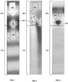
FIGs. 1 and 2 are respective cross-sectional views of a refractive-index sensor, in an embodiment. -
FIG. 3 is a three-dimensional view of an optics unit of the refractive-index sensor ofFIGs. 1 and 2 , in an embodiment. -
FIG. 4 illustrates electric field amplitudes of illumination incident upon, and propagating through, a dielectric resonator of a metasurface of the optics unit ofFIG. 3 , in an embodiment. -
FIG. 5 illustrates electric field amplitudes of an antisymmetric mode of a metasurface of the optics unit ofFIG. 3 , in an embodiment. -
FIG. 6 illustrates electric field amplitudes of illumination reflected by a metasurface of the optics unit ofFIG. 3 , in an embodiment. -
FIG. 7 is a transmittance plot of the metasurface of the optics unit ofFIG. 3 , in an embodiment. -
FIG. 8 is a transmittance plot of the metasurface associated withFIG. 7 for two refractive index values of encapsulant material, in an embodiment. -
FIG. 9 is a transmittance plot of the metasurface associated withFIG. 7 as a function of encapsulant refractive index, in an embodiment. -
FIG. 10 is a schematic illustrating a cross-section of a refractive-index sensor, which is an example of the refractive-index sensor ofFIGs. 1 and 2 . -
FIG. 11 is a schematic plot that includes a stopband of two metasurfaces of refractive-index sensors disclosed herein, in an embodiment. -
FIG. 12 is a transmittance plot of the metasurface associated withFIG. 7 for two refractive index values of encapsulant material filling, in an embodiment. -
FIG. 13 is a schematic illustrating a cross-section of a refractive-index sensor, which is an example of the refractive-index sensor ofFIG. 1 . -
FIG. 14 is a flowchart illustrating a method for measuring a refractive index of a medium, in an embodiment. -
FIG. 15 is a flowchart illustrating a method for distinguishing a change in refractive index from a change in illumination wavelength, in an embodiment. -
FIG. 1 is a cross-sectional view of a refractive-index sensor 100 in aplane 101 parallel to the x-z plane of acoordinate system 198. Hereinafter, directions and planes described by one or more axes x, y, and z refer to coordinatesystem 198 unless otherwise specified. - Refractive-
index sensor 100 includes anoptics unit 104 and alight source 150, and, in certain embodiments, aphotodetector 158.Optics unit 104 includes asubstrate 110, a plurality ofdielectric resonators 121 arranged as aperiodic array 120, and amicrofluidic chip 140.FIG. 2 is a cross-sectional view ofoptics unit 104 in across-sectional plane 102 that is parallel to the x-y plane.FIG. 3 is a three-dimensional view ofoptics unit 104, with a portion ofmicrofluidic chip 140 omitted to provide a clear view ofdielectric resonators 121.FIGs. 1-3 are best viewed together in the following description. -
Substrate 110 has atop surface 112.Microfluidic chip 140 is ontop surface 112 and has anon-planar bottom surface 141 that forms achannel 144 bounded betweentop surface 112 and a portion ofnon-planar bottom surface 141 not in contact withtop surface 112. Channel 144 has achannel depth 146 in a direction perpendicular totop surface 112. - Each
dielectric resonator 121 is ontop surface 112 and extends intochannel 144 to aheight 122 abovetop surface 112.Height 122 is less thanchannel depth 146. Eachdielectric resonator 121 has awidth 124.Periodic array 120 has aunit cell spacing 123, which is a center-to-center distance between nearest-neighbordielectric resonators 121. Whileresonators 121 have a circular cross-section in the example depicted inFIGs. 1-3 , they may have differently-shaped cross-sections, such as polygonal, without departing from the scope of the embodiments. -
Light source 150 is configured to illuminateperiodic array 120 withillumination 152 incident ontop surface 112 at anon-normal incident angle 156. Examples oflight source 150 include light-emitting diodes, fixed-wavelength lasers, and tunable lasers. In certain embodiments,illumination 152 is unpolarized. -
Illumination 152 has a center wavelength λ 0 exceeding each ofheight 122,width 124, andunit cell spacing 123. Eachdielectric resonator 121 has a refractive index nr (λ 0) andsubstrate 110 has a refractive index ns (λ o). In certain embodiments, illumination includesillumination 154 incident on a region 106 (FIG. 2 ) ofoptics unit 104 that does not includeperiodic array 120.Optics unit 104 transmits at least a portion ofillumination 154 as a reference signal 154T, which may be used for normalization, e.g., to determine a single-wavelength transmittance or transmittance spectrum ofmetasurface 130. -
Optics unit 104 transmits at least a portion ofincident illumination 152 as transmittedillumination 152T that, in embodiments, is detected byphotodetector 158. In operation, spectral properties of transmittedillumination 152T are used to measure the refractive index of anencapsulating medium 132 inchannel 144, as described herein. Encapsulatingmedium 132 may be a gas or a fluid. Encapsulatingmedium 132 andperiodic array 120 form ametasurface 130 withinchannel 144. InFIG. 1 , the callout referring tometasurface 130 touches a dashed box adjacent tosurfaces illumination 152 is narrower than a stopband ofmetasurface 130.Illumination 152 may have a center wavelength within the stopband.Light source 150 may include a bandpass filter to achieve said spectral bandwidth relationship. - In embodiments in accordance with the present invention,
metasurface 130 is a Huygens metasurface, that is, a metasurface with spectrally overlapping electric and magnetic dipole resonances. In certain other embodiments,metasurface 130 is not a Huygens metasurface, such that any overlap of electric dipole resonance and magnetic dipole resonance is insufficient for the metasurface to qualify as a Huygens metasurface. In such other embodiments, the electric dipole resonance is spectrally adjacent to the magnetic dipole resonance. For example, a spectral separation between the electric dipole resonance and an adjacent magnetic dipole resonance is at least one of (a) less than a linewidth ofillumination 152 and (b) greater than ½(δE + δB ), where δE and δB are respective spectral widths of the electric dipole resonance and the magnetic dipole resonance. - Herein, the refractive index of encapsulating medium 132 is referred to as the encapsulant refractive index. In embodiments, ns (λ 0) < αnr (λ 0) - β for sufficient refractive index contrast of
dielectric resonators 121 to the encapsulant refractive index to yield a stopband. In embodiments, coefficient α is between 0.6 and 0.7 and offset β is between 0.08 and 1.2. Coefficient α may equal the encapsulant refractive index divided by nr . The encapsulant refractive index may differ from substrate refractive index ns by less than offset β. -
FIG. 4 illustrates electric field amplitudes ofillumination 452 incident upon, and propagating through, one of a plurality ofdielectric resonators 421 of ametasurface 430 at a four-degree incidence angle.Metasurface 430 is onsubstrate 110 and has an electric dipole resonance that spectrally overlaps its magnetic dipole resonance at a center wavelength ofillumination 452. As a result,metasurface 430 transmits nearly one-hundred percent ofillumination 452 as transmittedillumination 453.Metasurface 430 is an example ofmetasurface 130. -
FIG. 5 illustrates electric field amplitudes ofillumination 552 incident upon one of a plurality ofdielectric resonators 421 ofmetasurface 430 at a wavelength that excites anantisymmetric mode 432 ofmetasurface 430. Indielectric resonators 421, the electric field amplitude ofillumination 552 is antisymmetric about aplane 592. As a result of a symmetry mismatch betweenincident illumination 552 and the excited an antisymmetric mode,metasurface 430 transmits only an evanescent field intosubstrate 110, rather than a propagating electromagnetic field in which energy flows intosubstrate 110. -
FIG. 6 illustrates electric field amplitudes ofillumination 652 normally-incident upon, and reflected by, one of a plurality ofdielectric resonators 521 of ametasurface 630.Metasurface 630 is onsubstrate 110 and has an electric dipole resonance that is spectrally adjacent to, and not overlapping with its magnetic dipole resonance. The center wavelength ofillumination 652 is between the respective electric and magnetic dipole resonance wavelengths ofmetasurface 630, which results inmetasurface 630 reflecting nearly one-hundred percent ofillumination 652 as reflectedillumination 653.Metasurface 630 is an example ofmetasurface 130. -
FIG. 7 is asimulated transmittance plot 790 for an embodiment ofmetasurface 130 that has spectrally overlapping electric and magnetic dipole resonances. In this embodiment, hereinafter embodiment A,substrate 110 is formed of SiO2, polydimethylsiloxane (PDMS) fillschannel 144, andheight 122, unit cell spacing 123, andwidth 124 are, respectively, 220 nm, 782 nm, and 482 nm. -
Transmittance plot 700 includes numerically-simulatedtransmittance spectra illumination 152 incident onoptics unit 104 atincidence angle 156 equal to zero degrees and four degrees, respectively.Transmittance spectrum 704 has astopband 710, which corresponds to an excitation of both the electric dipole resonance and the magnetic dipole resonance ofmetasurface 130 excited byillumination 152 incident at four-degrees.Stopband 710 has a center wavelength 712 and alinewidth 714. Center wavelength 712 is approximately 1237 nm. In one embodiment,illumination 152 has a spectral linewidth that is less thanlinewidth 714. In another embodiment,illumination 152 has a spectral linewidth that is exceedslinewidth 714. -
FIG. 8 is atransmittance plot 890 for embodiment A ofmetasurface 130 corresponding toFIG. 7 for two refractive index values of encapsulantmaterial filling channel 144.Transmittance plot 890 includes numerically-simulatedtransmittance spectra Transmittance spectra respective stopbands media 132, Δn = 0.005. In certain embodiments,illumination 152 has a spectral linewidth that is less than a linewidth of eitherstopband -
FIG. 9 is atransmittance plot 990 for embodiment A ofmetasurface 130 at λ = 1212.02 nm where the PDMS inchannel 144 has an encapsulant refractive index ranging from 1.333 to 1.338.Transmittance plot 990 includes numerically-simulated transmittance 910, and its derivative 912 (dT/dn) with respect to cavity refractive index. -
FIG. 10 is a schematic illustrating a cross-section of a refractive-index sensor 1000, which is an example of refractive-index sensor 100. Refractive-index sensor 1000 includes anoptics unit 1004 and alight source 1050, which are examples ofoptics unit 104 andlight source 150 respectively.Optics unit 1004 includesmicrofluidic chip 140 onsubstrate 110,periodic array 120, and a secondperiodic array 1020.Periodic arrays channel 144 betweensurfaces respective metasurfaces Light source 1050 is configured to simultaneously illuminate each ofperiodic array - Second
periodic array 1020 is an example ofperiodic array 120, and includes a plurality of second dielectric resonators arranged as secondperiodic array 1020 ontop surface 112. In embodiments, at least one of (i) a second width of each of the plurality of second dielectric resonators differs fromwidth 124 ofresonators 121 and (ii) a second unit cell size of the second periodic array differs from theunit cell size 123 ofresonators 121. In embodiments,periodic array 1020 is identical toperiodic array 120. - In certain embodiments, refractive-index sensor 1000 includes at least one of
photodetector 158 and aphotodetector 1058.Photodetector 1058 is configured to detect illumination 1052(2) transmitted bymetasurface 1030. -
FIG. 11 is aschematic transmittance plot 1190 that includes astopband 1110 ofmetasurface 130 and astopband 1120 ofmetasurface 1030. In one embodiment,stopbands respective metasurfaces illumination 1052, whereangle 156 is between two degrees and ten degrees. In another embodiment,stopbands respective metasurfaces illumination 1052, whereangle 156 is between negative two degrees and positive two degrees such thatillumination 1052 is at normal or near-normal incidence. -
Stopband 1110 has a center wavelength 1112 (λ 1) and a stopband linewidth 1114 (δλ 1).Stopband 1120 has a center wavelength 1122 (λ 2) and a stopband linewidth 1124 (δλ 2). In embodiments,illumination 1052 has an illumination center wavelength 1151 (λ 1151), that is between stopband center wavelengths 1112 and 1122: λ 1 < λ 1151 < λ 2. Also, in certain embodiments, stopband linewidth δλ 1 is greater than two times the spectral separation (λ 1151 - λ1) such that thestopband 1110 includes illumination center wavelength 1151 (λ 1151): (λ 1151 - λ 1) < 0.5δλ 1. Similarly, in embodiments, (λ 2 - λ0) < 0.5δλ2, such that thestopband 1120 also includes illumination center wavelength 1151 (λ1151). -
FIG. 12 is atransmittance plot 1290 of embodiment A ofmetasurface 130 for two refractive index values of encapsulatingmedium 132.Transmittance plot 1290 includes numerically-simulated stopbands Stopbands respective center wavelengths -
Stopbands stopbands illumination 1052 excites non-antisymmetric resonances (e.g., symmetric resonances) ofmetasurfaces transmittance plot 1290 is of embodiment A with two different encapsulant materials,periodic arrays stopbands -
Stopband 1210 results frommetasurface 130 having an electric dipole resonance, center wavelength λ E1210 thereof being less thancenter wavelength 1212, and a magnetic dipole resonance, center wavelength λ B1210 thereof being greater thancenter wavelength 1212. Similarly,stopband 1220 results frommetasurface 130 having an electric dipole resonance, center wavelength λ E1220 thereof being less thancenter wavelength 1222, and a magnetic dipole resonance, center wavelength λ B1220 thereof being greater thancenter wavelength 1222. Hence, each ofstopbands - Respective magnetic sides of
stopbands transmittance plot 1290,wavelength range 1231 is smaller thanwavelength range 1232. This occurs because the electric dipole resonance ofmetasurface 130 is more sensitive to encapsulant refractive index than is the magnetic dipole resonance. This asymmetry ofstopbands medium 132. - In certain embodiments,
metasurfaces stopbands metasurfaces metasurfaces medium 130 is a fluid that flows through and surrounds bothresonator arrays - When the encapsulant refractive index increases, both
stopbands FIG. 12 ), such that the detected transmittance ofmetasurface 130 decreases while the detected transmittance ofmetasurface 1030 increases. However, if center wavelength 1151 decreases, the detected transmittance ofmetasurface 130 decreases while the detected transmittance ofmetasurface 1030 increases. Hence, merely evaluating a whether transmittance increases or decreases is insufficient for distinguishing between center-wavelength drift and change in encapsulant refractive index. - Yet, if center wavelength 1151 correspond to the "electric" side of
stopband 1110 and the "magnetic" side ofstopband 1120, then, in response to a change in encapsulant refractive index, the transmittance of metasurface 130 (stopband 1110) will change more than that of metasurface 1030 (stopband 1120) because the electric dipole resonance is more sensitive to change in encapsulant refractive index. A drift in center wavelength 1151 would cause a significantly smaller transmittance-change difference betweenmetasurface - Other relationships between illumination center wavelengths and electric/magnetic dipole resonances result in the above-mentioned asymmetric wavelength shift that enables distinguishing between illumination wavelength drift and change in encapsulant refractive index. Examples of such relationships are described in the following. In an embodiment B, center wavelength 1112 of
stopband 1110 is determined by an electric dipole resonance and a magnetic dipole resonance ofmetasurface 130 having respective center wavelengths λ E1 and λ B1. In embodiment B,center wavelength 1122 ofstopband 1120 is determined by an electric dipole resonance and a magnetic dipole resonance of the second metasurface having respective center wavelengths λ E2 and λ B2. Whenillumination 1052 has an illumination center wavelength 1151 betweencenter wavelengths 1112 and 1122, either (i) λ E1 > λ B1 and λ E2 > λ B2 or (ii) λ E1 < λ B1 and λ E2 < λ B2. When both λ 1 and λ2 are either less than illumination center wavelength 1151 or greater than illumination center wavelength 1151, either (iii) λ E1 > λ B1 and λ E2 < λ B2 or (iv) λ E1 < λ B1 and λ E2 > λ B2. -
FIG. 13 is a schematic of a refractive-index sensor 1300, which is an example of refractive-index sensor 100. Refractive-index sensor 1300 includes alight source 1350, anoptics unit 1304, adetector 1358, and a post-processor 1310.Light sources light source 1350.Light source 1350 emitsillumination 1352, of whichillumination Optics units optics unit 1304 and transmits at least a portion ofillumination 1352 as transmittedillumination 1352T.Detector 1358 includes at least onedetector 158, such asphotodetector 1058,FIG. 10 . Post-processor 1310 includes aprocessor 1302 and amemory 1320.Detector 1358 is communicatively coupled to post-processor 1310, for example to one or both ofprocessor 1302 andmemory 1320. -
Memory 1320 may be transitory and/or non-transitory and may include one or both of volatile memory (e.g., SRAM, DRAM, computational RAM, other volatile memory, or any combination thereof) and non-volatile memory (e.g., FLASH, ROM, magnetic media, optical media, other non-volatile memory, or any combination thereof). Part or all ofmemory 1320 may be integrated intoprocessor 1302. -
Memory 1320 stores at least one of a referenceoptical signal 1321, a metasurfaceoptical signal 1322, a wavelength lookup table 1324, a transmittance lookup table 1326,software 1330, acenter wavelength 1342, and a measuredrefractive index 1348. An example of referenceoptical signal 1321 is output ofphotodetector 158 in response to transmitted illumination 154T. An example of metasurfaceoptical signal 1322 is output ofphotodetector 158 in response to transmittedillumination 152T. - Transmittance lookup table 1326 includes a plurality of transmittance values, such as simulated transmittance 910 (
FIG. 9 ), paired with a respective one of a plurality of candidate refractive indices (such as the abscissa of plot 990) of encapsulatingmedium 130. In certain embodiments, a full-wave electromagnetic simulation ofmetasurface 130 generates entries of at least one of lookup tables 1324 and 1326. -
Software 1330 includes at least one of astopband analyzer 1332, awavelength interpolator 1334, and atransmittance interpolator 1336. In embodiments,stopband analyzer 1332 determinescenter wavelength 1342 from transmittance spectra 1325. Examples ofcenter wavelengths 1342 includes center wavelength 712 (FIG. 7 ), respective center wavelengths λ = 1210 nm and λ = 1212 nm ofstopbands 803 and 808 (FIG. 8 ), center wavelengths 1112 and 1122 (FIG. 11 ), andcenter wavelengths 1212 and 1222 (FIG. 12 ). In embodiments,wavelength interpolator 1334 determines a measuredrefractive index 1348 fromcenter wavelength 1342 and wavelength lookup table 1324. -
FIG. 14 is a flowchart illustrating amethod 1400 for measuring a refractive index of a medium.Method 1400 may be implemented within one or more embodiments of refractive-index sensor 1300 to determine the encapsulant refractive index of encapsulatingmedium 132. In certain embodiments,software 1330encodes method 1400 as computer-readable instructions, andmethod 1400 is implemented byprocessor 1302 executing the computer-readable instructions ofsoftware 1330.Method 1400 includes at least one ofsteps -
Step 1410 includes exciting a first antisymmetric resonance of a first metasurface with illumination incident on the first metasurface at a non-normal incidence angle with respect to a substrate surface. The first metasurface includes a first periodic array of resonators formed on the substrate surface. The medium, whose refractive index is being measured, encapsulates the first periodic array of resonators. In an example ofstep 1410,optics unit 1304 of refractive-index sensor 1300 isoptics unit 1004, andlight source 1350 excites an antisymmetric resonance ofmetasurface 130 withillumination 1352. The medium is encapsulating medium 132. - In certain embodiments,
step 1410 includesstep 1412.Step 1412 includes exciting, with the illumination, a second antisymmetric resonance of a second metasurface including a second periodic array of resonators formed on a substrate surface, the second periodic array geometrically differing from the first periodic array. In certain embodiments, the incidence angle of the illumination on the second metasurface equals the incidence angle ofstep 1410. In an example ofstep 1412,light source 1050 excites an antisymmetric resonance ofmetasurface 1030 with illumination 1052(2),FIG. 10 . -
Step 1420 includes determining a refractive index of the medium from a first amplitude of a first transmitted signal that includes a portion of the illumination transmitted through the first metasurface. In an example ofstep 1420, refractive-index sensor 1300 determines measuredrefractive index 1348 of encapsulatingmedium 132. - In certain embodiments,
step 1420 includessteps -
Step 1422 includes determining center wavelength λ 1 from the first transmitted signal. In an example ofstep 1422,stopband analyzer 1332 determinescenter wavelength 1342 from metasurfaceoptical signal 1322, where metasurfaceoptical signal 1322 includes transmittance spectrum anddetector 1358 includes a spectrum analyzer. -
Step 1424 includes determining the refractive index at center wavelength λ 1 according to a lookup table that maps each of a plurality of stopband center-wavelengths to a respective one of a plurality of candidate refractive indices of the medium. In an example ofstep 1424,wavelength interpolator 1334 determines measuredrefractive index 1348 atcenter wavelength 1342 according to wavelength lookup table 1324. In this example, wavelength lookup table 1324 maps each of a plurality of stopband center-wavelengths to a respective one of a plurality of candidate refractive indices ofmedium 132. - In certain embodiments,
step 1420 includesstep 1426, which is applicable when a spectrum of the first transmitted signal has a stopband with a linewidth δλ 1 and the illumination has a center wavelength λ 0 and a spectral bandwidth less than linewidth δλ 1. In such embodiments,light source 1350 may be a fixed-wavelength source, which is more economical and space-efficient than a tunable source, andoptical signals detector 1358 may be single-wavelength measurements. -
Step 1426 includes determining the refractive index from the first transmitted signal according to a lookup table that maps each of a plurality of numerically-simulated transmittances of the medium, at center wavelength λ0, to a respective one of a plurality of refractive indices of the medium. In an example ofstep 1426,transmittance interpolator 1336 determines measuredrefractive index 1348 from metasurfaceoptical signal 1322, referenceoptical signal 1321, and transmittance lookup table 1326. - In certain embodiments,
step 1420 includesstep 1428, for example, whenstep 1410 includesstep 1412.Step 1428 includes determining the refractive index of the medium from a second amplitude of a second transmitted signal and the first amplitude, the second transmitted signal including a portion of the illumination transmitted through the second metasurface. In an example ofstep 1428, metasurfaceoptical signal 1322 includes a secondoptical signal 1323, which may be a transmitted-power spectrum or a single-wavelength transmitted power value ofmetasurface 1030.Software 1330 determines a second measured refractive index 1349 ofmetasurface 1030 via eithersteps step 1426. Post-processor 1310 may generate an error message when measured refractive index and second measured refractive index differ by more than a predetermined value. - In certain embodiments,
method 1400 includes bothsteps 1412 and asubsequent step 1430.Step 1430 includes determining whether a change in the first amplitude is caused by a change in center wavelength of the illumination or the change in the refractive index of the medium by comparing the change in the first amplitude to a change in the second amplitude.Step 1430 may apply when (a) the first metasurface has spectrally adjacent electric dipole and magnetic dipole resonances and (b) the second metasurface has spectrally adjacent electric dipole and magnetic dipole resonances. - In an example of
step 1430, metasurfaces 130 and 1030 of refractive index sensor 1000 haverespective stop bands FIG. 11 , andsoftware 1330 compares changes in transmittance ofmetasurfaces step 1430, metasurfaces 130 and 1030 have respective electric and magnetic dipole resonances per embodiment B described above. Also in this example ofstep 1430, whenillumination 1052 has an illumination center wavelength 1151 betweencenter wavelengths 1112 and 1122, either (i) λ E1 > λ B1 and λ E2 > λ B2 or (ii) λ E1 < λ B1 and λ E2 < λ B2. When both λ 1 and λ 2 are either less than illumination center wavelength 1151 or greater than illumination center wavelength 1151, either (iii) λ E1 > λ B1 and λ E2 < λ B2 or (iv) λ E1 < λ B1 and λ E2 > λ B2. -
FIG. 15 is a flowchart illustrating amethod 1500 for distinguishing a change in refractive index of a medium from a change of a center wavelength of illumination that illuminates the medium.Method 1500 may be implemented within one or more embodiments of refractive-index sensor 1300 to determine the encapsulant refractive index of encapsulatingmedium 132. In certain embodiments,software 1330encodes method 1400 as computer-readable instructions, andmethod 1500 is implemented byprocessor 1302 executing the computer-readable instructions ofsoftware 1330. -
Method 1500 includessteps respective steps method 1400. Insteps steps Steps step 1430 above.Method 1500 also includesstep 1530, which is similar to step 1430 ofmethod 1400. -
Step 1510 includes exciting a first resonance of a first metasurface with illumination incident on the first metasurface an incidence angle with respect to a substrate surface. The incidence angle may be zero degrees (normal incidence), near-normal incidence (between ±2 degrees) or between two degrees and ten degrees. The first resonance may be symmetric, antisymmetric, or non-antisymmetric. The first metasurface includes a first periodic array of resonators formed on the substrate surface. The medium, whose refractive index is being measured, encapsulates the first periodic array of resonators. In an example ofstep 1410,optics unit 1304 of refractive-index sensor 1300 isoptics unit 1004, andlight source 1350 excites a resonance ofmetasurface 130 withillumination 1352. The medium is encapsulating medium 132. -
Step 1512 includes exciting, with the illumination, a second resonance of a second metasurface including a second periodic array of resonators formed on a substrate surface, the second periodic array geometrically differing from the first periodic array. In certain embodiments, the incidence angle of the illumination on the second metasurface equals the incidence angle ofstep 1510. In an example ofstep 1412,light source 1050 excites a resonance ofmetasurface 1030 with illumination 1052(2),FIG. 10 . -
Step 1530 includes determining whether a change in a first amplitude, of a first transmitted signal, is caused by a change in the center wavelength of the illumination or a change in the refractive index of the medium by comparing the change in the first amplitude to a change in a second amplitude of a second transmitted signal. The first transmitted signal includes a first portion of the illumination transmitted through the first metasurface. The second transmitted signal includes a second portion of the illumination transmitted through the second metasurface. An example ofstep 1530 is the same as the example ofstep 1430 provided above.
Claims (8)
- A refractive-index sensor (100), comprising:a substrate (110) having a top surface (112);a microfluidic chip (140) on the top surface and having a non-planar bottom surface (141) that forms a channel (144) between the top surface and the non-planar bottom surface, the channel having a channel depth (146) in a direction perpendicular to the top surface;characterized in that the refractive-index sensor includes:a plurality of dielectric resonators (121) forming a metasurface (130,430,1030) on the top surface, each of the plurality of dielectric resonators extending into the channel to a height (122) above the top surface that is less than the channel depth, the metasurface having an electric dipole resonance and a magnetic dipole resonance that are either (i) spectrally overlapping or (ii) spectrally adjacent; anda light source (150) configured to illuminate the metasurface with illumination (152) incident on the top surface at an incidence angle (156), the illumination (152) having a center wavelength λ 0 exceeding the height (122), a width (124) of each of the plurality of dielectric resonators, and a unit cell size (123) of the metasurface.
- The refractive-index sensor (100) of claim 1, further comprising:a photodetector (158) configured to detect a transmitted signal that includes a portion of the illumination (152) transmitted through the substrate (110) and the metasurface (130,430,1030);a processor (1302) communicatively coupled to the photodetector; anda memory (1320) storing non-transitory computer-readable instructions that, when executed by the processor, control the processor to determine a refractive index, of an encapsulating medium (132) in the channel (144), from an amplitude of the transmitted signal.
- The refractive-index sensor (100) of claim 1, the incidence angle (156) being non-zero.
- The refractive-index sensor (100) of claim 1, each of the substrate (110) and microfluidic chip (140) being at least partially transmissive at the center wavelength λ 0.
- A method for sensing refractive index, comprising:illuminating, with the light source of the refractive-index sensor (100) of claim 1, the metasurface (130,430,1030) of the refractive-index sensor with illumination (152) to excite an optical resonance of the metasurface;detecting, with a photodetector (158), a transmitted signal that includes a portion of the illumination transmitted through the substrate (110) and the metasurface; anddetermining, based on a power of the transmitted signal, a refractive index of an encapsulant medium (132) in the channel (144) of the refractive-index sensor.
- The method of claim 5, further comprising flowing the encapsulant medium (132) through the channel (144).
- The method of claim 5, wherein:said illuminating the metasurface (130,430,1030) includes illuminating the metasurface with a first incident beam of the illumination (152);said detecting the transmitted signal includes detecting a first transmitted signal;the method further includes:illuminating, with a second incident beam of the illumination, a portion of the refractive-index sensor (100) adjacent to the metasurface; anddetecting a second transmitted signal that includes a portion of the second incident beam that is transmitted through the substrate (110) and the encapsulant medium (132) but not the metasurface; andsaid determining the refractive index is based on an intensity of each of the first and second transmitted signals.
- The method of claim 7, wherein said determining the refractive index includes normalizing the intensity of the first transmitted signal with the intensity of the second transmitted signal.
Applications Claiming Priority (2)
| Application Number | Priority Date | Filing Date | Title |
|---|---|---|---|
| US201862671707P | 2018-05-15 | 2018-05-15 | |
| PCT/US2019/031952 WO2019222070A1 (en) | 2018-05-15 | 2019-05-13 | Refractive-index sensor and method |
Publications (3)
| Publication Number | Publication Date |
|---|---|
| EP3793934A1 EP3793934A1 (en) | 2021-03-24 |
| EP3793934A4 EP3793934A4 (en) | 2021-12-29 |
| EP3793934B1 true EP3793934B1 (en) | 2025-02-19 |
Family
ID=68541053
Family Applications (1)
| Application Number | Title | Priority Date | Filing Date |
|---|---|---|---|
| EP19803795.4A Active EP3793934B1 (en) | 2018-05-15 | 2019-05-13 | Refractive-index sensor and method |
Country Status (4)
| Country | Link |
|---|---|
| US (2) | US11506602B2 (en) |
| EP (1) | EP3793934B1 (en) |
| CN (1) | CN112585083A (en) |
| WO (1) | WO2019222070A1 (en) |
Families Citing this family (9)
| Publication number | Priority date | Publication date | Assignee | Title |
|---|---|---|---|---|
| CN111198414B (en) * | 2020-01-13 | 2021-06-01 | 电子科技大学 | Self-biased magneto-optical nonreciprocal super-structured surface device |
| FR3107364B1 (en) * | 2020-02-19 | 2023-11-17 | Commissariat Energie Atomique | Optical component with encapsulated metasurface and method of manufacturing such a component |
| CN111650156B (en) * | 2020-06-15 | 2021-04-30 | 武汉理工大学 | High-quality-factor refractive index sensor based on all-dielectric super surface and manufacturing method thereof |
| CN112113916B (en) * | 2020-08-07 | 2023-03-31 | 华南师范大学 | Double-channel refractive index sensor and method based on all-dielectric super-surface |
| CN113376121A (en) * | 2021-06-01 | 2021-09-10 | 北京邮电大学 | high-Q-value super-surface refractive index sensor based on connection of double semicircular ring holes |
| CN113376122A (en) * | 2021-06-01 | 2021-09-10 | 北京邮电大学 | All-dielectric super-surface refractive index sensor based on four-rectangular silicon pillar structure |
| CN115356266B (en) * | 2022-08-25 | 2025-09-19 | 中国科学院微电子研究所 | Tunable measurement method and measurement system for super-surface device |
| CN119595592B (en) * | 2023-09-11 | 2025-10-10 | 中国科学院大连化学物理研究所 | A silicon-based metasurface large-range refractive index sensor |
| CN121253483B (en) * | 2025-12-08 | 2026-04-17 | 中国科学院西安光学精密机械研究所 | Compact fluid refractive index measurement system and fluid refractive index measurement method |
Family Cites Families (11)
| Publication number | Priority date | Publication date | Assignee | Title |
|---|---|---|---|---|
| US8111401B2 (en) * | 1999-11-05 | 2012-02-07 | Robert Magnusson | Guided-mode resonance sensors employing angular, spectral, modal, and polarization diversity for high-precision sensing in compact formats |
| US7118710B2 (en) | 2000-10-30 | 2006-10-10 | Sru Biosystems, Inc. | Label-free high-throughput optical technique for detecting biomolecular interactions |
| US7371562B2 (en) * | 2000-10-30 | 2008-05-13 | Sru Biosystems, Inc. | Guided mode resonant filter biosensor using a linear grating surface structure |
| AU2007319975B2 (en) * | 2006-11-09 | 2011-03-03 | Sru Biosystems, Inc. | Photonic crystal sensors with integrated fluid containment structure |
| CN102519907B (en) * | 2011-12-16 | 2014-11-05 | 浙江大学 | Reflection type refractive index sensor based on optical fibre and micro-fluidic chip |
| EP2942618B1 (en) * | 2014-05-09 | 2017-07-12 | Samsung Electronics Co., Ltd | Spectro-sensor and spectrometer employing the same |
| JP2017527857A (en) * | 2014-09-15 | 2017-09-21 | カリフォルニア インスティチュート オブ テクノロジー | Simultaneous polarization and wavefront control using planar devices |
| US9685765B2 (en) * | 2015-08-31 | 2017-06-20 | Sandia Corporation | High quality-factor fano metasurface comprising a single resonator unit cell |
| CN106092906B (en) * | 2016-08-15 | 2019-01-18 | 福州大学 | A kind of circular dichroism spectra and refractometry system based on linearly polarized light incidence |
| EP3451027A1 (en) * | 2017-09-01 | 2019-03-06 | Thomson Licensing | Optical device capable of providing at least two different optical functions |
| CN107579328B (en) * | 2017-09-26 | 2020-01-14 | 中国计量大学 | E-shaped full-medium super-surface electromagnetic induction transparent resonance device |
-
2019
- 2019-05-13 CN CN201980046169.1A patent/CN112585083A/en active Pending
- 2019-05-13 US US17/055,833 patent/US11506602B2/en active Active
- 2019-05-13 EP EP19803795.4A patent/EP3793934B1/en active Active
- 2019-05-13 WO PCT/US2019/031952 patent/WO2019222070A1/en not_active Ceased
-
2022
- 2022-01-03 US US17/567,677 patent/US20220128464A1/en not_active Abandoned
Also Published As
| Publication number | Publication date |
|---|---|
| US20220128464A1 (en) | 2022-04-28 |
| WO2019222070A1 (en) | 2019-11-21 |
| CN112585083A (en) | 2021-03-30 |
| EP3793934A4 (en) | 2021-12-29 |
| EP3793934A1 (en) | 2021-03-24 |
| US20210223170A1 (en) | 2021-07-22 |
| US11506602B2 (en) | 2022-11-22 |
Similar Documents
| Publication | Publication Date | Title |
|---|---|---|
| US20220128464A1 (en) | Refractive-index sensor and method | |
| CN105899983B (en) | Guided Mode Resonance Equipment | |
| KR102138607B1 (en) | Critical angle optical sensor apparatus | |
| JP4909285B2 (en) | Single mode (SM) fiber optic reader system and method for interrogating a resonant waveguide grating sensor | |
| US20080298740A1 (en) | Integrated Optical Waveguide Sensors With Reduced Signal Modulation | |
| US6661938B2 (en) | Optical micro-cavity sensors | |
| US9335263B2 (en) | Optical circuit for sensing a biological entity in a fluid and method of configuring the same | |
| CN101413881A (en) | System for measuring gas concentration of optical fiber grating with tunable filtering characteristic | |
| US20100182606A1 (en) | Apparatus and method for multi-parameter optical measurements | |
| CN103884683B (en) | Based on the optical sensor of F-P semiconductor laser and the cascade of film F-P optical filter | |
| EP2053385A2 (en) | Apparatus and method for detecting the presence of an agent | |
| US9068950B2 (en) | Vernier photonic sensor data-analysis | |
| WO2014198409A1 (en) | Integrated optical waveguide sensor system | |
| CN108801455A (en) | A kind of excitation of Raman optical signal and collection device | |
| JP2005091467A (en) | Photonic crystal optical functional element | |
| Gupta et al. | A novel leaky waveguide grating (LWG) device for evanescent wave broadband absorption spectroscopy in microfluidic flow cells | |
| US20230417992A1 (en) | Optical sensor chip and optical sensing system | |
| KR102715035B1 (en) | Optical filter and spectrometer including sub-wavelength reflector, and electronic apparatus including the spectrometer | |
| JP5311852B2 (en) | Sensing device | |
| JP5365594B2 (en) | Refractive index measuring apparatus and refractive index measuring method using guided mode resonance grating | |
| CN114018402B (en) | Optical resonant cavity sensing signal enhancement method | |
| JPS62159027A (en) | Detecting device for degree of deterioration of oil | |
| RU2773389C1 (en) | Integrated optical sensor for determining the content of impurities in gas-air media | |
| EP4103929B1 (en) | Method of analysis of refractive index using a polarisation-sensitive optical sensor and sensor system comprising the optical sensor | |
| Wang et al. | Silicon chip-based dual Fabry–Pérot biosensor employing the Vernier effect for enhanced sensitivity |
Legal Events
| Date | Code | Title | Description |
|---|---|---|---|
| STAA | Information on the status of an ep patent application or granted ep patent |
Free format text: STATUS: THE INTERNATIONAL PUBLICATION HAS BEEN MADE |
|
| PUAI | Public reference made under article 153(3) epc to a published international application that has entered the european phase |
Free format text: ORIGINAL CODE: 0009012 |
|
| STAA | Information on the status of an ep patent application or granted ep patent |
Free format text: STATUS: REQUEST FOR EXAMINATION WAS MADE |
|
| 17P | Request for examination filed |
Effective date: 20201203 |
|
| AK | Designated contracting states |
Kind code of ref document: A1 Designated state(s): AL AT BE BG CH CY CZ DE DK EE ES FI FR GB GR HR HU IE IS IT LI LT LU LV MC MK MT NL NO PL PT RO RS SE SI SK SM TR |
|
| AX | Request for extension of the european patent |
Extension state: BA ME |
|
| DAV | Request for validation of the european patent (deleted) | ||
| DAX | Request for extension of the european patent (deleted) | ||
| A4 | Supplementary search report drawn up and despatched |
Effective date: 20211129 |
|
| RIC1 | Information provided on ipc code assigned before grant |
Ipc: B82Y 20/00 20110101ALN20211123BHEP Ipc: B82Y 15/00 20110101ALN20211123BHEP Ipc: B01L 3/00 20060101ALI20211123BHEP Ipc: G02F 1/00 20060101ALI20211123BHEP Ipc: G02B 5/00 20060101ALI20211123BHEP Ipc: G02B 1/00 20060101ALI20211123BHEP Ipc: G01N 21/41 20060101AFI20211123BHEP |
|
| REG | Reference to a national code |
Ref country code: DE Ref legal event code: R079 Free format text: PREVIOUS MAIN CLASS: B82Y0020000000 Ipc: G01N0021410000 Ref document number: 602019066224 Country of ref document: DE |
|
| STAA | Information on the status of an ep patent application or granted ep patent |
Free format text: STATUS: EXAMINATION IS IN PROGRESS |
|
| RIC1 | Information provided on ipc code assigned before grant |
Ipc: B82Y 20/00 20110101ALN20220804BHEP Ipc: B82Y 15/00 20110101ALN20220804BHEP Ipc: G02B 1/00 20060101ALI20220804BHEP Ipc: G01N 21/41 20060101AFI20220804BHEP |
|
| RIC1 | Information provided on ipc code assigned before grant |
Ipc: B82Y 20/00 20110101ALN20220808BHEP Ipc: B82Y 15/00 20110101ALN20220808BHEP Ipc: G02B 1/00 20060101ALI20220808BHEP Ipc: G01N 21/41 20060101AFI20220808BHEP |
|
| 17Q | First examination report despatched |
Effective date: 20220819 |
|
| P01 | Opt-out of the competence of the unified patent court (upc) registered |
Effective date: 20230519 |
|
| GRAP | Despatch of communication of intention to grant a patent |
Free format text: ORIGINAL CODE: EPIDOSNIGR1 |
|
| STAA | Information on the status of an ep patent application or granted ep patent |
Free format text: STATUS: GRANT OF PATENT IS INTENDED |
|
| RIC1 | Information provided on ipc code assigned before grant |
Ipc: B82Y 20/00 20110101ALN20240327BHEP Ipc: B82Y 15/00 20110101ALN20240327BHEP Ipc: G02B 1/00 20060101ALI20240327BHEP Ipc: G01N 21/41 20060101AFI20240327BHEP |
|
| RIC1 | Information provided on ipc code assigned before grant |
Ipc: B82Y 20/00 20110101ALN20240408BHEP Ipc: B82Y 15/00 20110101ALN20240408BHEP Ipc: G02B 1/00 20060101ALI20240408BHEP Ipc: G01N 21/41 20060101AFI20240408BHEP |
|
| INTG | Intention to grant announced |
Effective date: 20240424 |
|
| GRAS | Grant fee paid |
Free format text: ORIGINAL CODE: EPIDOSNIGR3 |
|
| GRAL | Information related to payment of fee for publishing/printing deleted |
Free format text: ORIGINAL CODE: EPIDOSDIGR3 |
|
| GRAJ | Information related to disapproval of communication of intention to grant by the applicant or resumption of examination proceedings by the epo deleted |
Free format text: ORIGINAL CODE: EPIDOSDIGR1 |
|
| STAA | Information on the status of an ep patent application or granted ep patent |
Free format text: STATUS: EXAMINATION IS IN PROGRESS |
|
| GRAS | Grant fee paid |
Free format text: ORIGINAL CODE: EPIDOSNIGR3 |
|
| STAA | Information on the status of an ep patent application or granted ep patent |
Free format text: STATUS: GRANT OF PATENT IS INTENDED |
|
| GRAP | Despatch of communication of intention to grant a patent |
Free format text: ORIGINAL CODE: EPIDOSNIGR1 |
|
| INTC | Intention to grant announced (deleted) | ||
| INTG | Intention to grant announced |
Effective date: 20240910 |
|
| RIC1 | Information provided on ipc code assigned before grant |
Ipc: B82Y 20/00 20110101ALN20240902BHEP Ipc: B82Y 15/00 20110101ALN20240902BHEP Ipc: G02B 1/00 20060101ALI20240902BHEP Ipc: G01N 21/41 20060101AFI20240902BHEP |
|
| GRAA | (expected) grant |
Free format text: ORIGINAL CODE: 0009210 |
|
| STAA | Information on the status of an ep patent application or granted ep patent |
Free format text: STATUS: THE PATENT HAS BEEN GRANTED |
|
| AK | Designated contracting states |
Kind code of ref document: B1 Designated state(s): AL AT BE BG CH CY CZ DE DK EE ES FI FR GB GR HR HU IE IS IT LI LT LU LV MC MK MT NL NO PL PT RO RS SE SI SK SM TR |
|
| REG | Reference to a national code |
Ref country code: GB Ref legal event code: FG4D |
|
| REG | Reference to a national code |
Ref country code: CH Ref legal event code: EP |
|
| REG | Reference to a national code |
Ref country code: DE Ref legal event code: R096 Ref document number: 602019066224 Country of ref document: DE |
|
| REG | Reference to a national code |
Ref country code: IE Ref legal event code: FG4D |
|
| REG | Reference to a national code |
Ref country code: NL Ref legal event code: MP Effective date: 20250219 |
|
| PG25 | Lapsed in a contracting state [announced via postgrant information from national office to epo] |
Ref country code: RS Free format text: LAPSE BECAUSE OF FAILURE TO SUBMIT A TRANSLATION OF THE DESCRIPTION OR TO PAY THE FEE WITHIN THE PRESCRIBED TIME-LIMIT Effective date: 20250519 |
|
| PG25 | Lapsed in a contracting state [announced via postgrant information from national office to epo] |
Ref country code: FI Free format text: LAPSE BECAUSE OF FAILURE TO SUBMIT A TRANSLATION OF THE DESCRIPTION OR TO PAY THE FEE WITHIN THE PRESCRIBED TIME-LIMIT Effective date: 20250219 |
|
| PG25 | Lapsed in a contracting state [announced via postgrant information from national office to epo] |
Ref country code: PL Free format text: LAPSE BECAUSE OF FAILURE TO SUBMIT A TRANSLATION OF THE DESCRIPTION OR TO PAY THE FEE WITHIN THE PRESCRIBED TIME-LIMIT Effective date: 20250219 |
|
| PG25 | Lapsed in a contracting state [announced via postgrant information from national office to epo] |
Ref country code: ES Free format text: LAPSE BECAUSE OF FAILURE TO SUBMIT A TRANSLATION OF THE DESCRIPTION OR TO PAY THE FEE WITHIN THE PRESCRIBED TIME-LIMIT Effective date: 20250219 |
|
| REG | Reference to a national code |
Ref country code: LT Ref legal event code: MG9D |
|
| PG25 | Lapsed in a contracting state [announced via postgrant information from national office to epo] |
Ref country code: NO Free format text: LAPSE BECAUSE OF FAILURE TO SUBMIT A TRANSLATION OF THE DESCRIPTION OR TO PAY THE FEE WITHIN THE PRESCRIBED TIME-LIMIT Effective date: 20250519 Ref country code: IS Free format text: LAPSE BECAUSE OF FAILURE TO SUBMIT A TRANSLATION OF THE DESCRIPTION OR TO PAY THE FEE WITHIN THE PRESCRIBED TIME-LIMIT Effective date: 20250619 |
|
| PG25 | Lapsed in a contracting state [announced via postgrant information from national office to epo] |
Ref country code: NL Free format text: LAPSE BECAUSE OF FAILURE TO SUBMIT A TRANSLATION OF THE DESCRIPTION OR TO PAY THE FEE WITHIN THE PRESCRIBED TIME-LIMIT Effective date: 20250219 |
|
| PG25 | Lapsed in a contracting state [announced via postgrant information from national office to epo] |
Ref country code: HR Free format text: LAPSE BECAUSE OF FAILURE TO SUBMIT A TRANSLATION OF THE DESCRIPTION OR TO PAY THE FEE WITHIN THE PRESCRIBED TIME-LIMIT Effective date: 20250219 |
|
| PG25 | Lapsed in a contracting state [announced via postgrant information from national office to epo] |
Ref country code: PT Free format text: LAPSE BECAUSE OF FAILURE TO SUBMIT A TRANSLATION OF THE DESCRIPTION OR TO PAY THE FEE WITHIN THE PRESCRIBED TIME-LIMIT Effective date: 20250620 Ref country code: LV Free format text: LAPSE BECAUSE OF FAILURE TO SUBMIT A TRANSLATION OF THE DESCRIPTION OR TO PAY THE FEE WITHIN THE PRESCRIBED TIME-LIMIT Effective date: 20250219 |
|
| PG25 | Lapsed in a contracting state [announced via postgrant information from national office to epo] |
Ref country code: GR Free format text: LAPSE BECAUSE OF FAILURE TO SUBMIT A TRANSLATION OF THE DESCRIPTION OR TO PAY THE FEE WITHIN THE PRESCRIBED TIME-LIMIT Effective date: 20250520 Ref country code: BG Free format text: LAPSE BECAUSE OF FAILURE TO SUBMIT A TRANSLATION OF THE DESCRIPTION OR TO PAY THE FEE WITHIN THE PRESCRIBED TIME-LIMIT Effective date: 20250219 |
|
| REG | Reference to a national code |
Ref country code: AT Ref legal event code: MK05 Ref document number: 1768698 Country of ref document: AT Kind code of ref document: T Effective date: 20250219 |
|
| PG25 | Lapsed in a contracting state [announced via postgrant information from national office to epo] |
Ref country code: SE Free format text: LAPSE BECAUSE OF FAILURE TO SUBMIT A TRANSLATION OF THE DESCRIPTION OR TO PAY THE FEE WITHIN THE PRESCRIBED TIME-LIMIT Effective date: 20250219 |
|
| PG25 | Lapsed in a contracting state [announced via postgrant information from national office to epo] |
Ref country code: SM Free format text: LAPSE BECAUSE OF FAILURE TO SUBMIT A TRANSLATION OF THE DESCRIPTION OR TO PAY THE FEE WITHIN THE PRESCRIBED TIME-LIMIT Effective date: 20250219 |
|
| PG25 | Lapsed in a contracting state [announced via postgrant information from national office to epo] |
Ref country code: DK Free format text: LAPSE BECAUSE OF FAILURE TO SUBMIT A TRANSLATION OF THE DESCRIPTION OR TO PAY THE FEE WITHIN THE PRESCRIBED TIME-LIMIT Effective date: 20250219 |
|
| PG25 | Lapsed in a contracting state [announced via postgrant information from national office to epo] |
Ref country code: IT Free format text: LAPSE BECAUSE OF FAILURE TO SUBMIT A TRANSLATION OF THE DESCRIPTION OR TO PAY THE FEE WITHIN THE PRESCRIBED TIME-LIMIT Effective date: 20250219 |
|
| PG25 | Lapsed in a contracting state [announced via postgrant information from national office to epo] |
Ref country code: AT Free format text: LAPSE BECAUSE OF FAILURE TO SUBMIT A TRANSLATION OF THE DESCRIPTION OR TO PAY THE FEE WITHIN THE PRESCRIBED TIME-LIMIT Effective date: 20250219 |
|
| PG25 | Lapsed in a contracting state [announced via postgrant information from national office to epo] |
Ref country code: CZ Free format text: LAPSE BECAUSE OF FAILURE TO SUBMIT A TRANSLATION OF THE DESCRIPTION OR TO PAY THE FEE WITHIN THE PRESCRIBED TIME-LIMIT Effective date: 20250219 Ref country code: EE Free format text: LAPSE BECAUSE OF FAILURE TO SUBMIT A TRANSLATION OF THE DESCRIPTION OR TO PAY THE FEE WITHIN THE PRESCRIBED TIME-LIMIT Effective date: 20250219 |
|
| PG25 | Lapsed in a contracting state [announced via postgrant information from national office to epo] |
Ref country code: RO Free format text: LAPSE BECAUSE OF FAILURE TO SUBMIT A TRANSLATION OF THE DESCRIPTION OR TO PAY THE FEE WITHIN THE PRESCRIBED TIME-LIMIT Effective date: 20250219 |
|
| PG25 | Lapsed in a contracting state [announced via postgrant information from national office to epo] |
Ref country code: SK Free format text: LAPSE BECAUSE OF FAILURE TO SUBMIT A TRANSLATION OF THE DESCRIPTION OR TO PAY THE FEE WITHIN THE PRESCRIBED TIME-LIMIT Effective date: 20250219 |
|
| REG | Reference to a national code |
Ref country code: DE Ref legal event code: R097 Ref document number: 602019066224 Country of ref document: DE |
|
| REG | Reference to a national code |
Ref country code: CH Ref legal event code: H13 Free format text: ST27 STATUS EVENT CODE: U-0-0-H10-H13 (AS PROVIDED BY THE NATIONAL OFFICE) Effective date: 20251223 |
|
| PLBE | No opposition filed within time limit |
Free format text: ORIGINAL CODE: 0009261 |
|
| STAA | Information on the status of an ep patent application or granted ep patent |
Free format text: STATUS: NO OPPOSITION FILED WITHIN TIME LIMIT |
|
| PG25 | Lapsed in a contracting state [announced via postgrant information from national office to epo] |
Ref country code: LU Free format text: LAPSE BECAUSE OF NON-PAYMENT OF DUE FEES Effective date: 20250513 |
|
| PG25 | Lapsed in a contracting state [announced via postgrant information from national office to epo] |
Ref country code: CH Free format text: LAPSE BECAUSE OF NON-PAYMENT OF DUE FEES Effective date: 20250531 |
|
| 26N | No opposition filed |
Effective date: 20251120 |
|
| GBPC | Gb: european patent ceased through non-payment of renewal fee |
Effective date: 20250519 |
|
| REG | Reference to a national code |
Ref country code: BE Ref legal event code: MM Effective date: 20250531 |
|
| PG25 | Lapsed in a contracting state [announced via postgrant information from national office to epo] |
Ref country code: MC Free format text: LAPSE BECAUSE OF FAILURE TO SUBMIT A TRANSLATION OF THE DESCRIPTION OR TO PAY THE FEE WITHIN THE PRESCRIBED TIME-LIMIT Effective date: 20250219 |
|
| PG25 | Lapsed in a contracting state [announced via postgrant information from national office to epo] |
Ref country code: GB Free format text: LAPSE BECAUSE OF NON-PAYMENT OF DUE FEES Effective date: 20250519 |
|
| PG25 | Lapsed in a contracting state [announced via postgrant information from national office to epo] |
Ref country code: IE Free format text: LAPSE BECAUSE OF NON-PAYMENT OF DUE FEES Effective date: 20250513 |
|
| PG25 | Lapsed in a contracting state [announced via postgrant information from national office to epo] |
Ref country code: BE Free format text: LAPSE BECAUSE OF NON-PAYMENT OF DUE FEES Effective date: 20250531 |
|
| PG25 | Lapsed in a contracting state [announced via postgrant information from national office to epo] |
Ref country code: LT Free format text: LAPSE BECAUSE OF FAILURE TO SUBMIT A TRANSLATION OF THE DESCRIPTION OR TO PAY THE FEE WITHIN THE PRESCRIBED TIME-LIMIT Effective date: 20250219 |
|
| PGFP | Annual fee paid to national office [announced via postgrant information from national office to epo] |
Ref country code: DE Payment date: 20260331 Year of fee payment: 8 |
|
| PGFP | Annual fee paid to national office [announced via postgrant information from national office to epo] |
Ref country code: FR Payment date: 20260401 Year of fee payment: 8 |
|
| PG25 | Lapsed in a contracting state [announced via postgrant information from national office to epo] |
Ref country code: CY Free format text: LAPSE BECAUSE OF FAILURE TO SUBMIT A TRANSLATION OF THE DESCRIPTION OR TO PAY THE FEE WITHIN THE PRESCRIBED TIME-LIMIT Effective date: 20250219 |