EP3792953A1 - Control method for electron microscope and electron microscope - Google Patents
Control method for electron microscope and electron microscope Download PDFInfo
- Publication number
- EP3792953A1 EP3792953A1 EP20195345.2A EP20195345A EP3792953A1 EP 3792953 A1 EP3792953 A1 EP 3792953A1 EP 20195345 A EP20195345 A EP 20195345A EP 3792953 A1 EP3792953 A1 EP 3792953A1
- Authority
- EP
- European Patent Office
- Prior art keywords
- filament
- condition
- current
- thermionic
- value
- Prior art date
- Legal status (The legal status is an assumption and is not a legal conclusion. Google has not performed a legal analysis and makes no representation as to the accuracy of the status listed.)
- Granted
Links
Images



Classifications
-
- H—ELECTRICITY
- H01—ELECTRIC ELEMENTS
- H01J—ELECTRIC DISCHARGE TUBES OR DISCHARGE LAMPS
- H01J37/00—Discharge tubes with provision for introducing objects or material to be exposed to the discharge, e.g. for the purpose of examination or processing thereof
- H01J37/02—Details
- H01J37/04—Arrangements of electrodes and associated parts for generating or controlling the discharge, e.g. electron-optical arrangement or ion-optical arrangement
- H01J37/06—Electron sources; Electron guns
- H01J37/075—Electron guns using thermionic emission from cathodes heated by particle bombardment or by irradiation, e.g. by laser
-
- H—ELECTRICITY
- H01—ELECTRIC ELEMENTS
- H01J—ELECTRIC DISCHARGE TUBES OR DISCHARGE LAMPS
- H01J37/00—Discharge tubes with provision for introducing objects or material to be exposed to the discharge, e.g. for the purpose of examination or processing thereof
- H01J37/26—Electron or ion microscopes; Electron or ion diffraction tubes
- H01J37/261—Details
- H01J37/265—Controlling the tube; circuit arrangements adapted to a particular application not otherwise provided, e.g. bright-field-dark-field illumination
-
- H—ELECTRICITY
- H01—ELECTRIC ELEMENTS
- H01J—ELECTRIC DISCHARGE TUBES OR DISCHARGE LAMPS
- H01J37/00—Discharge tubes with provision for introducing objects or material to be exposed to the discharge, e.g. for the purpose of examination or processing thereof
- H01J37/02—Details
- H01J37/24—Circuit arrangements not adapted to a particular application of the tube and not otherwise provided for
- H01J37/241—High voltage power supply or regulation circuits
-
- H—ELECTRICITY
- H01—ELECTRIC ELEMENTS
- H01J—ELECTRIC DISCHARGE TUBES OR DISCHARGE LAMPS
- H01J37/00—Discharge tubes with provision for introducing objects or material to be exposed to the discharge, e.g. for the purpose of examination or processing thereof
- H01J37/02—Details
- H01J37/24—Circuit arrangements not adapted to a particular application of the tube and not otherwise provided for
- H01J37/243—Beam current control or regulation circuits
-
- H—ELECTRICITY
- H01—ELECTRIC ELEMENTS
- H01J—ELECTRIC DISCHARGE TUBES OR DISCHARGE LAMPS
- H01J37/00—Discharge tubes with provision for introducing objects or material to be exposed to the discharge, e.g. for the purpose of examination or processing thereof
- H01J37/26—Electron or ion microscopes; Electron or ion diffraction tubes
- H01J37/28—Electron or ion microscopes; Electron or ion diffraction tubes with scanning beams
-
- H—ELECTRICITY
- H01—ELECTRIC ELEMENTS
- H01J—ELECTRIC DISCHARGE TUBES OR DISCHARGE LAMPS
- H01J2237/00—Discharge tubes exposing object to beam, e.g. for analysis treatment, etching, imaging
- H01J2237/06—Sources
- H01J2237/063—Electron sources
- H01J2237/06308—Thermionic sources
-
- H—ELECTRICITY
- H01—ELECTRIC ELEMENTS
- H01J—ELECTRIC DISCHARGE TUBES OR DISCHARGE LAMPS
- H01J2237/00—Discharge tubes exposing object to beam, e.g. for analysis treatment, etching, imaging
- H01J2237/245—Detection characterised by the variable being measured
- H01J2237/24507—Intensity, dose or other characteristics of particle beams or electromagnetic radiation
- H01J2237/24514—Beam diagnostics including control of the parameter or property diagnosed
- H01J2237/24535—Beam current
Definitions
- the present invention relates to a control method for an electron microscope and an electron microscope.
- a thermionic-emission gun As an electron gun used in an electron microscope, a thermionic-emission gun is known. As the thermionic-emission gun, there is used a thermionic-emission gun that uses a filament made of tungsten or a thermionic-emission gun that uses a filament made of a single crystal of lanthanum boride (LaB 6 ).
- the filament when the filament is replaced, there may be a case where the brightness of the electron gun changes due to misalignment in a step of manufacturing the filament or an installation error of the filament.
- an amount of an illumination current i.e., a probe current
- an observation result or an analysis result is influenced, and hence continuous observation or analysis is hindered.
- EDS analysis when the probe current changes due to replacement of the filament, it is not possible to simply compare an EDS spectrum obtained before the replacement of the filament with an EDS spectrum obtained after the replacement of the filament.
- a control method for an electron microscope including a thermionic-emission gun of self-bias type using a fixed bias resistor, an accelerating voltage power supply supplying an accelerating voltage to the thermionic-emission gun, and an optical system for irradiating a specimen with an electron beam, the control method including:
- an electron microscope including:
- control section sets the condition of the optical system based on the filament height, and hence it is possible to reduce the change of the probe current caused by the replacement of the filament.
- FIG. 1 is a diagram illustrating a configuration of an electron microscope 100 according to an embodiment of the invention.
- the electron microscope 100 includes an electron gun 10, an accelerating voltage power supply 20, an optical system 30, a detector 40, an amplifier 42, an AD converter 44, an alignment power supply 50, a condenser lens power supply 52, an objective lens power supply 54, a scanning signal generating circuit 56, and a control device 60 (an example of a control section).
- the electron gun 10 emits an electron beam.
- the electron gun 10 is a thermionic-emission gun.
- the thermionic-emission gun is an electron gun which uses thermionic emission.
- the electron gun 10 includes a cathode 12, a Wehnelt electrode 14, an anode 16, and a bias resistor 18.
- the cathode 12 is, e.g., a filament made of tungsten. Note that the cathode 12 may also be a filament made of a single crystal of lanthanum boride (LaB 6 ).
- the Wehnelt electrode 14 is disposed between the cathode 12 and the anode 16. A minus bias voltage is applied to the cathode 12, and the Wehnelt electrode 14 is used to control the amount of emitted electrons.
- the anode 16 is, e.g., a ground potential, and acceleration energy of the electron beam to a specimen S is determined by a potential difference between the cathode 12 and the anode 16. A crossover is formed by lens action of the cathode 12, the Wehnelt electrode 14, and the anode 16.
- the bias resistor 18 is a resistor for generating a self-bias voltage.
- the bias resistor 18 is disposed between the cathode 12 and the Wehnelt electrode 14.
- the resistance value of the bias resistor 18 is fixed.
- the electron gun 10 is a thermionic-emission gun of self-bias type using the fixed bias resistor 18.
- thermoelectron is emitted by heating the cathode 12.
- the emitted electron is accelerated by the accelerating voltage applied between the cathode 12 and the anode 16.
- An emission current is controlled by a bias voltage applied to the Wehnelt electrode 14.
- the emission current is an electron current emitted from the electron gun 10.
- the crossover is formed by the lens action of the cathode 12, the Wehnelt electrode 14, and the anode 16.
- the electron gun 10 a voltage generated in the bias resistor 18 by the passage of the emission current through the bias resistor 18 is used as the bias voltage. With this, the emission current is limited. The bias voltage is proportional to the emission current.
- the electron gun 10 is the thermionic-emission gun of self-bias type in which the bias voltage is dependent on the emission current.
- the bias voltage i.e., the self-bias voltage
- a voltage corresponding to a voltage drop caused when the whole emission current passes through the bias resistor 18 is applied between the cathode 12 and the Wehnelt electrode 14, and a type of feedback action is generated. Accordingly, even when a factor which fluctuates the emission current occurs, the fluctuation of the emission current is reduced by the action of the self-bias voltage. Consequently, in the electron gun 10, it is possible to stabilize the emission current.
- the accelerating voltage power supply 20 supplies an accelerating voltage for accelerating electrons.
- the accelerating voltage is a voltage applied between the cathode 12 and the anode 16.
- the accelerating voltage power supply 20 has an ammeter 22 for measuring the value of a load current.
- the load current is a current passing through the accelerating voltage power supply 20, and is obtained by adding the emission current to a current passing through the accelerating voltage power supply 20 for generating the accelerating voltage.
- the optical system 30 includes a first alignment coil 32a, a second alignment coil 32b, a condenser lens 34, an objective aperture 35, an objective lens 36, and a deflection coil 38.
- Each of the first alignment coil 32a and the second alignment coil 32b deflects an electron beam emitted from the electron gun 10.
- the first alignment coil 32a and the second alignment coil 32b are used in, e.g., GUN alignment.
- the GUN alignment denotes axis alignment in which the electron beam emitted from the electron gun 10 is deflected so as to coincide with the optical axis of the condenser lens 34.
- the condenser lens 34 condenses the electron beam.
- the condenser lens 34 is used to control the probe current and a probe diameter. For example, when excitation of the condenser lens 34 is strengthened, the amount of electrons passing through the objective aperture 35 is reduced and, when the excitation of the condenser lens 34 is weakened, the amount of electrons passing through the objective aperture 35 is increased. In addition, when the excitation of the condenser lens 34 is strengthened, a focal length is reduced, and the reduction ratio of an electron probe is increased. By using these functions, it is possible to control the probe current and the probe diameter.
- the probe current is a current passing through the electron probe applied to a specimen.
- the objective lens 36 is a lens for focusing the electron probe onto a specimen surface.
- the electron beam is condensed and focused and the electron probe is formed by the condenser lens 34 and the objective lens 36.
- the deflection coil 38 is a coil for performing scanning of the electron probe.
- the scanning of the electron probe is performed by supplying a scanning signal to the deflection coil 38.
- the detector 40 detects electrons generated by irradiating the specimen S with the electron beam.
- a signal detected by the detector 40 is amplified in the amplifier 42 and is then converted to a digital signal by the AD converter 44, and the digital signal is sent to the control device 60.
- the alignment power supply 50 supplies an alignment current to the first alignment coil 32a and the second alignment coil 32b.
- the condenser lens power supply 52 supplies an excitation current to the condenser lens 34.
- the objective lens power supply 54 supplies the excitation current to the objective lens 36.
- the scanning signal generating circuit 56 generates a scanning signal, and supplies the scanning signal to the deflection coil 38.
- the control device 60 controls individual sections constituting the electron microscope 100.
- the control device 60 includes, e.g., a central processing unit (CPU), a storage device (random access memory (RAM)), and a read only memory (ROM).
- CPU central processing unit
- RAM random access memory
- ROM read only memory
- the CPU executes programs stored in the storage device to thereby perform various calculation processing and various control processing.
- the control device 60 controls the scanning signal generating circuit 56 such that a desired area of the specimen S is scanned by the electron probe.
- the scanning signal is supplied to the deflection coil 38 from the scanning signal generating circuit 56, and the desired area of the specimen S is scanned by the electron probe.
- Electrons generated by irradiating the specimen S with the electron beam are detected by the detector 40, and a detection signal is amplified by the amplifier 42 and is then sent to the control device 60.
- the control device 60 generates the SEM image based on the detection signal.
- control device 60 controls the condenser lens power supply 52 such that the change of the probe current caused by the replacement of the filament of the electron gun 10 is reduced.
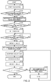
- FIG. 2 is a flowchart illustrating an example of processing of the control device 60 after the filament of the electron gun 10 is replaced.
- each of an optical column and a specimen chamber of the electron microscope 100 has atmospheric pressure. Accordingly, a vacuum pump is operated and the evacuation of the optical column and the specimen chamber is started (S100).
- the control device 60 monitors the degree of vacuum measured by a vacuum gauge disposed in each of the optical column and the specimen chamber and, in the case where a predetermined degree of vacuum is reached (Yes in S102), the control device 60 notifies a user that observation can be performed (S104).
- the notification to the user is performed by, e.g., displaying an image notifying the user that that observation can be performed in a display section such as, e.g., a liquid crystal display.
- the control device 60 When the control device 60 receives input of an observation start instruction from the user (Yes in S 106), the control device 60 sets observation conditions of the SEM image in the accelerating voltage power supply 20, the alignment power supply 50, the condenser lens power supply 52, the objective lens power supply 54, and the scanning signal generating circuit 56 (S 108).
- the observation conditions of the SEM image may be preset initial conditions of SEM image observation, or may also be observation conditions of the SEM image input by the user.
- the control device 60 waits for a preset predetermined time period (S110). With this, it is possible to stabilize the individual sections constituting the electron microscope 100.
- the predetermined time period is, e.g., from 10 seconds to 60 seconds.
- the control device 60 After a lapse of the predetermined time period (Yes in S110), the control device 60 obtains the value of a load current I L0 from the ammeter 22 of the accelerating voltage power supply 20 (S112).
- the control device 60 sets the condition of the condenser lens 34 based on the obtained value of the load current I L0 (S114). Specifically, the control device 60 determines a filament height based on the obtained value of the load current I L0 , and determines the condition of the condenser lens 34 based on the determined filament height. The control device 60 controls the condenser lens power supply 52 such that the determined condition of the condenser lens 34 is achieved. With this, the condenser lens 34 has the determined condition. The detail of a setting method of the condition of the condenser lens 34 will be described later.
- the control device 60 performs adjustment of the GUN alignment (S118).
- the control device 60 operates the first alignment coil 32a and the second alignment coil 32b such that the electron beam emitted from the electron gun 10 coincides with the optical axis of the condenser lens 34.
- the operation of each of the first alignment coil 32a and the second alignment coil 32b can be controlled by controlling the alignment power supply 50.
- the control device 60 executes known automatic GUN alignment to thereby perform the alignment adjustment.
- the adjustment of the GUN alignment is performed by moving the electron beam in two directions in a plane to search for optimum conditions by controlling the excitation current supplied to two alignment coils (the first alignment coil 32a and the second alignment coil 32b).
- the excitation current supplied to two alignment coils the first alignment coil 32a and the second alignment coil 32b.
- the adjustment of the GUN alignment is performed during the time period for stabilizing the condenser lens 34 in the present processing, and hence the adjustment of the GUN alignment is performed efficiently, and it is possible to reduce a time period required before the observation can be started after the filament replacement.
- control device 60 performs adjustment of focus (S 120).
- the control device 60 operates the objective lens 36 such that the optimum focus is obtained.
- the operation of the objective lens 36 can be controlled by controlling the objective lens power supply 54.
- the control device 60 executes known autofocus to thereby perform the adjustment of the focus. Note that the above-described gain adjustment may be performed also when the adjustment of the focus is performed.
- control device 60 obtains the value of a load current I L1 from the ammeter 22 of the accelerating voltage power supply 20 (S122).
- the control device 60 determines a difference between the value of the load current I L1 and the value of the load current I L0 , and determines whether or not the difference is less than a preset reference value ⁇ I L (S124). That is, it is determined whether or not
- the control device 60 sets the condition of the condenser lens 34 based on the obtained value of the load current I L1 (S 126). Specifically, the control device 60 determines the filament height based on the obtained value of the load current I L1 , and determines the condition of the condenser lens 34 based on the determined filament height. The control device 60 controls the condenser lens power supply 52 such that the determined condition of the condenser lens 34 is achieved. With this, the condenser lens 34 has the determined condition. The detail of a setting method of the condition of the condenser lens 34 will be described later.
- control device 60 sets the condition of the condenser lens 34 based on the obtained value of the load current I L1 , the control device 60 sets the value of the load current I L1 as the value of the load current I L0 (S128), and returns to Step S118. Subsequently, the control device 60 repeats the steps of the processing Step S118, Step S120, Step S122, Step S124, Step S126, and Step S128 until
- Processing operations of setting the condition of the condenser lens 34 S116 and S126 include processing of determining the filament height based on the obtained value of the load current I L0 , and processing of setting the condition of the condenser lens 34 based on the determined filament height.
- the filament height is a distance between the tip of the filament and the tip of the Wehnelt electrode 14 (see a filament height H in FIG. 5 ).
- FIG. 3 is a graph illustrating a relationship between the value of the load current I L and the filament height H.
- FIG. 3 illustrates the relationship between the value of the load current I L and the filament height H for each accelerating voltage. Specifically, FIG. 3 illustrates the relationship between the value of the load current I L and the filament height H in the case where the accelerating voltage is 5 kV, the relationship between the value of the load current I L and the filament height H in the case where the accelerating voltage is 10 kV, and the relationship between the value of the load current I L and the filament height H in the case where the accelerating voltage is 15 kV.
- FIG. 4 is a table 2 illustrating a relationship between the filament height H and the condition of the condenser lens 34.
- the condition (excitation current) of the condenser lens 34 is determined by the filament height H and the desired probe current.
- the probe current can be set to five levels consisting of Biggest, Large, Middle, Standard, and Small.
- the probe current is about 10 nA in the case of Biggest
- the probe current is about 2 nA in the case of Large
- the probe current is about 400 pA in the case of Middle
- the probe current is about 80 pA in the case of Standard
- the probe current is about 16 pA in the case of Small.
- the probe current can be optionally selected by the user. For example, in the case where a large probe current is required as in the case of EDS analysis, Biggest or Large is selected and, in the case of normal SEM observation, Middle or Standard is selected. In addition, in the case where a specimen vulnerable to the electron beam is observed, Small is selected. With regard to the selection of the probe current, for example, the user may input the desired probe current together with an instruction to start the observation. Note that the probe current may also be set in advance.
- the excitation current of the condenser lens 34 is a1 [A].
- the excitation current of the condenser lens 34 is b3 [A].
- the excitation current is selected as the condition of the condenser lens 34, but the condition of the condenser lens 34 is not limited thereto, and the condition of the condenser lens 34 may be any condition as long as the condition is a control value for controlling the condenser lens 34.
- a control value includes a DAC value.
- FIGS. 5 and 6 illustrate an evaluation result of the crossover by electric field simulation.
- measurement is performed at an accelerating voltage of 15 kV while the filament height H is changed. Note that a bias electric field is corrected based on the result of the value of the load current I L illustrated in FIG. 3 .
- FIG. 5 illustrates the case where the filament height H is in the vicinity of 0.4 mm, and the value of the load current is about 100 ⁇ A.
- FIG. 6 illustrates the case where the filament height H is in the vicinity of 0.6 mm, and the value of the load current is about 60 ⁇ A.
- the bias resistor is set to 4 M ⁇
- the electron emitted from the filament is a thermoelectron, and hence, in reality, the initial energy has an energy distribution wider than 0.1 eV. Consequently, the actual operation of the electron gun does not completely coincide with examples in FIGS. 5 and 6 . However, a little increase or decrease in initial energy does not significantly change the position of the crossover, and the change of the filament height H changes the position of the crossover more significantly than the increase or decrease in initially energy. The change of the brightness of the electron gun has been studied with the same filament used and the filament height changed.
- FIG. 7 is a graph illustrating a relationship between the filament height H and the probe current Ip.
- the graph in FIG. 7 is a result obtained by measuring the change of the probe current Ip in the case where the condition of the condenser lens is constant and the condition of the GUN alignment is optimized when the same combination of the filament and the Wehnelt electrode is used and the filament height H is changed.
- the change of the probe current Ip in FIG. 7 is obtained when the condition of the condenser lens is constant. Consequently, the change of the probe current Ip corresponds to the change of the brightness of the electron gun.
- the brightness denotes a quantity indicative of the intensity of the electron gun, and is expressed in terms of a current density per unit solid angle.
- the change of the probe current Ip includes the change of the position of the crossover described above, and the change of the position of the crossover is small relative to a distance from the position of the crossover to the condenser lens. For example, while the distance from the position of the crossover to the condenser lens is several centimeters, the change of the position of the crossover is several millimeters or less. Accordingly, the change of the probe current Ip (i.e., the change of the brightness) caused by the change of the position of the cross over is considered to be extremely small (e.g., 10% or less).
- the graph is divided into an area A close to the Wehnelt electrode, an area B in which brightness is reduced, an area C in which optimum brightness is obtained, and an area D in which brightness is reduced.
- Each of the area A and the area B has a condition which has a weak bias effect, and the area D has an extremely strong bias effect, and hence the brightness is reduced.
- the bias effect denotes a degree of limitation of the emission current by the bias voltage and, as the bias effect becomes stronger, the emission current is limited more significantly.
- the bias voltage is determined by the value of the load current including dark current, and the bias effect is changed by the filament height H.
- a maximum brightness condition is present before a cut-off voltage, and the brightness is reduced under a condition which weakens the bias effect before the maximum brightness condition.
- the area B, the area C, and the area D satisfy the above relationship.
- the bias effect is weak in the area A, and hence the probe current is increased and the apparent brightness is increased, but the area A has a problem in which the crossover is split into a plurality of bright spots, and hence this condition is not the optimum bias condition. From this, when the filament height H is in the area C, the bias effect is optimized and high brightness is obtained.
- the graph in FIG. 7 illustrates the change of the probe current when the condition of the condenser lens is fixed and the filament height H is changed, and the condition of the condenser lens which makes the probe current constant is used for setting the condition of the condenser lens.
- This condition has a curve similar to that in the graph in FIG. 7 and the curve can be approximately formed by using three or more curves.
- the table 2 in FIG. 4 collectively illustrates the conditions of the condenser lens which make the probe current constant when the filament height is changed.
- the probe current Ip is represented by the following relational expression: I p AccV , C 1 , H ⁇ ⁇ A AccV , C 1 ⁇ H 3 + B AccV , C 1 ⁇ H 2 ⁇ C AccV , C 1 ⁇ H + D AccV , C 1 wherein Ip is the probe current, AccV is the accelerating voltage, and C1 is the condition of the condenser lens.
- Ip is the probe current
- AccV is the accelerating voltage
- C1 is the condition of the condenser lens.
- A, B, C, and D are coefficients which change individually according to the filament height H.
- the above table 2 can be created from the above expression.
- a control method for an electron microscope including the thermionic-emission gun 10 of self-bias type using the fixed bias resistor 18, the accelerating voltage power supply 20 supplying the accelerating voltage to the thermionic-emission gun 10, and the condenser lens 34 for irradiating the specimen with the electron beam, the control method including: obtaining the value of the load current which is the current passing through the accelerating voltage power supply 20; determining the filament height H of the thermionic-emission gun 10 based on the value of the load current; and setting the condition of the condenser lens 34 based on the filament height H. Consequently, it is possible to reduce the change of the probe current caused by the replacement of the filament.
- the filament has been abandoned as a defective filament.
- the desired probe current is obtained by the action of the condenser lens 34, and hence the filament can be used.
- the filament having a filament height of about 0.45 mm which is positioned in the area B has been abandoned because the sufficient probe current is not obtained.
- the filament positioned in the area B it is possible to obtain the same probe current as that of the area C by the action of the condenser lens 34, and hence the filament can be used.
- the filament height H is determined based on the value of the load current and the condition of the condenser lens 34 is set based on the filament height H, and hence it is possible to easily set the condition of the condenser lens 34.
- the probe current needs to be measured by using a Faraday cup or the like. In the present embodiment, it is only necessary to obtain the value of the load current which can be easily obtained, and hence it is possible to easily set the condition of the condenser lens 34.
- the thermionic-emission gun of self-bias type 10 using the fixed bias resistor 18 is used, and hence it is possible to adopt the configuration which is smaller and simpler than that of a thermionic-emission gun in which the bias resistor can be varied.
- each of the filament made of tungsten and the filament made of the single crystal of lanthanum boride (LaB 6 ) is described as the filament used as the cathode 12 of the electron gun 10, the material of the filament is not limited thereto.
- the material of the filament used as the cathode 12 include Ta, Nb, Mo, Ru, Rh, V, Ti, and Ni.
- a metal wire to which Th, Y 2 O 3 , ThO 2 , Ba, CeO 2 , Os, or Ir is applied or a metal wire filament containing one of these metals may be used. With this, it is possible to reduce a work function on a metal surface, and hence it is possible to lower heating temperature and implement a long-life electron source.
- a filament made of a single crystal of CeB 6 , CaB 6 , BaB 6 , ZrC, SiC, TaC, TiC, or NbC may also be used.
- an impregnated cathode including an emissive material made of BaO, CaO, or Al 2 O 3 in sintered porous tungsten is formed into a chip of which an emissive surface at a tip is rounded and the chip is mounted to a tip of a metal wire, and the metal wire having the impregnated cathode may also be used as the cathode 12 of the electron gun 10.
- FIGS. 8 and 9 schematically illustrate part of the electron gun 10 of the electron microscope 100. Note that, in FIG. 9 , part of the electron gun 10 is separated into constituent members and the constituent members are illustrated.
- the filament in the electron gun 10, the filament can be replaced by replacing a filament unit 102.
- a spacer 104 can be disposed between the filament unit 102 and the Wehnelt electrode 14.
- the filament height can be adjusted by changing the number of spacers 104 disposed between the filament unit 102 and the Wehnelt electrode 14.
- the invention includes configurations that are substantially the same as the configurations described in the embodiments.
- Substantially same configurations means configurations that are the same in function and method, for example.
- the invention also includes configurations in which non-essential elements described in the embodiments are replaced by other elements.
- the invention further includes configurations obtained by adding known art to the configurations described in the embodiments.
Landscapes
- Chemical & Material Sciences (AREA)
- Analytical Chemistry (AREA)
- Physics & Mathematics (AREA)
- Optics & Photonics (AREA)
- Electron Sources, Ion Sources (AREA)
Abstract
Description
- The present invention relates to a control method for an electron microscope and an electron microscope.
- As an electron gun used in an electron microscope, a thermionic-emission gun is known. As the thermionic-emission gun, there is used a thermionic-emission gun that uses a filament made of tungsten or a thermionic-emission gun that uses a filament made of a single crystal of lanthanum boride (LaB6).
- In such a thermionic-emission gun, in a case where the filament is degraded, replacement of the filament is required (see, e.g.,
JP-A-2018-106899 - However, when the filament is replaced, there may be a case where the brightness of the electron gun changes due to misalignment in a step of manufacturing the filament or an installation error of the filament. When the brightness of the electron gun changes, there may be a case where an amount of an illumination current, i.e., a probe current, significantly changes. Thus, when the probe current significantly changes, an observation result or an analysis result is influenced, and hence continuous observation or analysis is hindered. For example, in EDS analysis, when the probe current changes due to replacement of the filament, it is not possible to simply compare an EDS spectrum obtained before the replacement of the filament with an EDS spectrum obtained after the replacement of the filament.
- According to a first aspect of the invention, there is provided a control method for an electron microscope including a thermionic-emission gun of self-bias type using a fixed bias resistor, an accelerating voltage power supply supplying an accelerating voltage to the thermionic-emission gun, and an optical system for irradiating a specimen with an electron beam, the control method including:
- obtaining a value of a load current which is a current passing through the accelerating voltage power supply;
- determining a filament height of the thermionic-emission gun based on the value of the load current; and
- setting a condition of the optical system based on the filament height.
- According to a second aspect of the invention, there is provided an electron microscope including:
- a thermionic-emission gun of self-bias type using a fixed bias resistor;
- an accelerating voltage power supply supplying an accelerating voltage to the thermionic-emission gun;
- an ammeter measuring a value of a load current which is a current passing through the accelerating voltage power supply;
- an optical system for irradiating a specimen with an electron beam; and
- a control section controlling the thermionic-emission gun and the optical system,
- the control section performing:
- processing of obtaining the value of the load current;
- processing of determining a filament height of the thermionic-emission gun based on the value of the load current; and
- processing of setting a condition of the optical system based on the filament height.
-
-
FIG. 1 is a diagram illustrating a configuration of an electron microscope according to an embodiment of the invention. -
FIG. 2 is a flowchart illustrating an example of processing of a control device. -
FIG. 3 is a graph illustrating a relationship between a value of a load current and a filament height. -
FIG. 4 is a table illustrating a relationship between a filament height and a condition of a condenser lens. -
FIG. 5 illustrates an evaluation result of a crossover by electric field simulation. -
FIG. 6 illustrates an evaluation result of a crossover by electric field simulation. -
FIG. 7 is a graph illustrating a relationship between a filament height and a probe current. -
FIG. 8 schematically illustrates part of an electron gun. -
FIG. 9 schematically illustrates part of an electron gun. -
- (1) According to an embodiment of the invention, there is provided a control method for an electron microscope including a thermionic-emission gun of self-bias type using a fixed bias resistor, an accelerating voltage power supply supplying an accelerating voltage to the thermionic-emission gun, and an optical system for irradiating a specimen with an electron beam, the control method including:
- obtaining a value of a load current which is a current passing through the accelerating voltage power supply;
- determining a filament height of the thermionic-emission gun based on the value of the load current; and
- setting a condition of the optical system based on the filament height.
In the control method for an electron microscope described above, the condition of the optical system is set based on the filament height, and hence it is possible to reduce change of a probe current caused by replacement of the filament.
- (2) According to the embodiment of the invention, there is provided an electron microscope including:
- a thermionic-emission gun of self-bias type using a fixed bias resistor;
- an accelerating voltage power supply supplying an accelerating voltage to the thermionic-emission gun;
- an ammeter measuring a value of a load current which is a current passing through the accelerating voltage power supply;
- an optical system for irradiating a specimen with an electron beam; and
- a control section controlling the thermionic-emission gun and the optical system,
- the control section performing:
- processing of obtaining the value of the load current;
- processing of determining a filament height of the thermionic-emission gun based on the value of the load current; and
- processing of setting a condition of the optical system based on the filament height.
- In the electron microscope described above, the control section sets the condition of the optical system based on the filament height, and hence it is possible to reduce the change of the probe current caused by the replacement of the filament.
- Preferred embodiments of the invention are described in detail below with reference to the drawings. It is noted that the following embodiments do not unduly limit the scope of the invention as stated in the claims. In addition, all of the elements described below are not necessarily essential requirements of the invention.
- First, an electron microscope according to an embodiment of the invention will be described with reference to the drawings.
FIG. 1 is a diagram illustrating a configuration of anelectron microscope 100 according to an embodiment of the invention. - The
electron microscope 100 includes anelectron gun 10, an acceleratingvoltage power supply 20, anoptical system 30, adetector 40, anamplifier 42, anAD converter 44, analignment power supply 50, a condenserlens power supply 52, an objectivelens power supply 54, a scanningsignal generating circuit 56, and a control device 60 (an example of a control section). - The
electron gun 10 emits an electron beam. Theelectron gun 10 is a thermionic-emission gun. The thermionic-emission gun is an electron gun which uses thermionic emission. Theelectron gun 10 includes acathode 12, aWehnelt electrode 14, ananode 16, and abias resistor 18. - The
cathode 12 is, e.g., a filament made of tungsten. Note that thecathode 12 may also be a filament made of a single crystal of lanthanum boride (LaB6). TheWehnelt electrode 14 is disposed between thecathode 12 and theanode 16. A minus bias voltage is applied to thecathode 12, and theWehnelt electrode 14 is used to control the amount of emitted electrons. Theanode 16 is, e.g., a ground potential, and acceleration energy of the electron beam to a specimen S is determined by a potential difference between thecathode 12 and theanode 16. A crossover is formed by lens action of thecathode 12, theWehnelt electrode 14, and theanode 16. - The
bias resistor 18 is a resistor for generating a self-bias voltage. Thebias resistor 18 is disposed between thecathode 12 and theWehnelt electrode 14. The resistance value of thebias resistor 18 is fixed. Theelectron gun 10 is a thermionic-emission gun of self-bias type using the fixedbias resistor 18. - In the
electron gun 10, a thermoelectron is emitted by heating thecathode 12. The emitted electron is accelerated by the accelerating voltage applied between thecathode 12 and theanode 16. An emission current is controlled by a bias voltage applied to theWehnelt electrode 14. The emission current is an electron current emitted from theelectron gun 10. The crossover is formed by the lens action of thecathode 12, theWehnelt electrode 14, and theanode 16. - Herein, in the
electron gun 10, a voltage generated in thebias resistor 18 by the passage of the emission current through thebias resistor 18 is used as the bias voltage. With this, the emission current is limited. The bias voltage is proportional to the emission current. Thus, theelectron gun 10 is the thermionic-emission gun of self-bias type in which the bias voltage is dependent on the emission current. - With regard to the bias voltage, i.e., the self-bias voltage, a voltage corresponding to a voltage drop caused when the whole emission current passes through the
bias resistor 18 is applied between thecathode 12 and theWehnelt electrode 14, and a type of feedback action is generated. Accordingly, even when a factor which fluctuates the emission current occurs, the fluctuation of the emission current is reduced by the action of the self-bias voltage. Consequently, in theelectron gun 10, it is possible to stabilize the emission current. - The accelerating
voltage power supply 20 supplies an accelerating voltage for accelerating electrons. The accelerating voltage is a voltage applied between thecathode 12 and theanode 16. The acceleratingvoltage power supply 20 has anammeter 22 for measuring the value of a load current. The load current is a current passing through the acceleratingvoltage power supply 20, and is obtained by adding the emission current to a current passing through the acceleratingvoltage power supply 20 for generating the accelerating voltage. - The
optical system 30 includes afirst alignment coil 32a, asecond alignment coil 32b, acondenser lens 34, anobjective aperture 35, anobjective lens 36, and adeflection coil 38. - Each of the
first alignment coil 32a and thesecond alignment coil 32b deflects an electron beam emitted from theelectron gun 10. Thefirst alignment coil 32a and thesecond alignment coil 32b are used in, e.g., GUN alignment. The GUN alignment denotes axis alignment in which the electron beam emitted from theelectron gun 10 is deflected so as to coincide with the optical axis of thecondenser lens 34. - The
condenser lens 34 condenses the electron beam. Thecondenser lens 34 is used to control the probe current and a probe diameter. For example, when excitation of thecondenser lens 34 is strengthened, the amount of electrons passing through theobjective aperture 35 is reduced and, when the excitation of thecondenser lens 34 is weakened, the amount of electrons passing through theobjective aperture 35 is increased. In addition, when the excitation of thecondenser lens 34 is strengthened, a focal length is reduced, and the reduction ratio of an electron probe is increased. By using these functions, it is possible to control the probe current and the probe diameter. The probe current is a current passing through the electron probe applied to a specimen. - The
objective lens 36 is a lens for focusing the electron probe onto a specimen surface. The electron beam is condensed and focused and the electron probe is formed by thecondenser lens 34 and theobjective lens 36. - The
deflection coil 38 is a coil for performing scanning of the electron probe. The scanning of the electron probe is performed by supplying a scanning signal to thedeflection coil 38. - The
detector 40 detects electrons generated by irradiating the specimen S with the electron beam. A signal detected by thedetector 40 is amplified in theamplifier 42 and is then converted to a digital signal by theAD converter 44, and the digital signal is sent to thecontrol device 60. - The
alignment power supply 50 supplies an alignment current to thefirst alignment coil 32a and thesecond alignment coil 32b. The condenserlens power supply 52 supplies an excitation current to thecondenser lens 34. The objectivelens power supply 54 supplies the excitation current to theobjective lens 36. The scanningsignal generating circuit 56 generates a scanning signal, and supplies the scanning signal to thedeflection coil 38. - The
control device 60 controls individual sections constituting theelectron microscope 100. Thecontrol device 60 includes, e.g., a central processing unit (CPU), a storage device (random access memory (RAM)), and a read only memory (ROM). In thecontrol device 60, the CPU executes programs stored in the storage device to thereby perform various calculation processing and various control processing. - Next, the operation of the
electron microscope 100 will be described. First, a description will be given of the case where a scanning electron microscope image (SEM image) is obtained in theelectron microscope 100. - In the case where the SEM image is obtained in the
electron microscope 100, thecontrol device 60 controls the scanningsignal generating circuit 56 such that a desired area of the specimen S is scanned by the electron probe. With this, the scanning signal is supplied to thedeflection coil 38 from the scanningsignal generating circuit 56, and the desired area of the specimen S is scanned by the electron probe. Electrons generated by irradiating the specimen S with the electron beam are detected by thedetector 40, and a detection signal is amplified by theamplifier 42 and is then sent to thecontrol device 60. Thecontrol device 60 generates the SEM image based on the detection signal. - Next, a description will be given of an operation when the
electron microscope 100 is activated after the replacement of the filament of theelectron gun 10. In theelectron microscope 100, thecontrol device 60 controls the condenserlens power supply 52 such that the change of the probe current caused by the replacement of the filament of theelectron gun 10 is reduced. -
FIG. 2 is a flowchart illustrating an example of processing of thecontrol device 60 after the filament of theelectron gun 10 is replaced. - After the replacement of the filament, each of an optical column and a specimen chamber of the
electron microscope 100 has atmospheric pressure. Accordingly, a vacuum pump is operated and the evacuation of the optical column and the specimen chamber is started (S100). Thecontrol device 60 monitors the degree of vacuum measured by a vacuum gauge disposed in each of the optical column and the specimen chamber and, in the case where a predetermined degree of vacuum is reached (Yes in S102), thecontrol device 60 notifies a user that observation can be performed (S104). The notification to the user is performed by, e.g., displaying an image notifying the user that that observation can be performed in a display section such as, e.g., a liquid crystal display. - When the
control device 60 receives input of an observation start instruction from the user (Yes in S 106), thecontrol device 60 sets observation conditions of the SEM image in the acceleratingvoltage power supply 20, thealignment power supply 50, the condenserlens power supply 52, the objectivelens power supply 54, and the scanning signal generating circuit 56 (S 108). The observation conditions of the SEM image may be preset initial conditions of SEM image observation, or may also be observation conditions of the SEM image input by the user. - The
control device 60 waits for a preset predetermined time period (S110). With this, it is possible to stabilize the individual sections constituting theelectron microscope 100. The predetermined time period is, e.g., from 10 seconds to 60 seconds. - After a lapse of the predetermined time period (Yes in S110), the
control device 60 obtains the value of a load current IL0 from theammeter 22 of the accelerating voltage power supply 20 (S112). - The
control device 60 sets the condition of thecondenser lens 34 based on the obtained value of the load current IL0 (S114). Specifically, thecontrol device 60 determines a filament height based on the obtained value of the load current IL0, and determines the condition of thecondenser lens 34 based on the determined filament height. Thecontrol device 60 controls the condenserlens power supply 52 such that the determined condition of thecondenser lens 34 is achieved. With this, thecondenser lens 34 has the determined condition. The detail of a setting method of the condition of thecondenser lens 34 will be described later. - Next, the
control device 60 performs adjustment of the GUN alignment (S118). For example, thecontrol device 60 operates thefirst alignment coil 32a and thesecond alignment coil 32b such that the electron beam emitted from theelectron gun 10 coincides with the optical axis of thecondenser lens 34. The operation of each of thefirst alignment coil 32a and thesecond alignment coil 32b can be controlled by controlling thealignment power supply 50. For example, thecontrol device 60 executes known automatic GUN alignment to thereby perform the alignment adjustment. - Herein, the adjustment of the GUN alignment is performed by moving the electron beam in two directions in a plane to search for optimum conditions by controlling the excitation current supplied to two alignment coils (the
first alignment coil 32a and thesecond alignment coil 32b). In order to perform the adjustment of the GUN alignment, it is necessary to optimize a signal amount detected by thedetector 40. It is possible to optimize the signal amount by using, e.g., gain adjustment by known automatic contrast-brightness adjustment. Thus, although it takes time to perform the adjustment of the GUN alignment, the adjustment of the GUN alignment is performed during the time period for stabilizing thecondenser lens 34 in the present processing, and hence the adjustment of the GUN alignment is performed efficiently, and it is possible to reduce a time period required before the observation can be started after the filament replacement. - Next, the
control device 60 performs adjustment of focus (S 120). Thecontrol device 60 operates theobjective lens 36 such that the optimum focus is obtained. The operation of theobjective lens 36 can be controlled by controlling the objectivelens power supply 54. For example, thecontrol device 60 executes known autofocus to thereby perform the adjustment of the focus. Note that the above-described gain adjustment may be performed also when the adjustment of the focus is performed. - Next, the
control device 60 obtains the value of a load current IL1 from theammeter 22 of the accelerating voltage power supply 20 (S122). - The
control device 60 determines a difference between the value of the load current IL1 and the value of the load current IL0, and determines whether or not the difference is less than a preset reference value ΔIL (S124). That is, it is determined whether or not |IL1 - IL0| < ΔIL is satisfied. With this, it is possible to determine whether or not the value of the load current is stabilized. - In the case where it is determined that |IL1 - IL0| < ΔIL is not satisfied (No in S 124), the
control device 60 sets the condition of thecondenser lens 34 based on the obtained value of the load current IL1 (S 126). Specifically, thecontrol device 60 determines the filament height based on the obtained value of the load current IL1, and determines the condition of thecondenser lens 34 based on the determined filament height. Thecontrol device 60 controls the condenserlens power supply 52 such that the determined condition of thecondenser lens 34 is achieved. With this, thecondenser lens 34 has the determined condition. The detail of a setting method of the condition of thecondenser lens 34 will be described later. - After the
control device 60 sets the condition of thecondenser lens 34 based on the obtained value of the load current IL1, thecontrol device 60 sets the value of the load current IL1 as the value of the load current IL0 (S128), and returns to Step S118. Subsequently, thecontrol device 60 repeats the steps of the processing Step S118, Step S120, Step S122, Step S124, Step S126, and Step S128 until |IL1 - IL0| < ΔIL is satisfied. - In the case where it is determined that |IL1 - IL0| < ΔIL is satisfied (Yes in S124), the
control device 60 ends the processing. - Next, a description will be given of processing of setting the condition of the
condenser lens 34. Processing operations of setting the condition of thecondenser lens 34 S116 and S126 include processing of determining the filament height based on the obtained value of the load current IL0, and processing of setting the condition of thecondenser lens 34 based on the determined filament height. The filament height is a distance between the tip of the filament and the tip of the Wehnelt electrode 14 (see a filament height H inFIG. 5 ). -
FIG. 3 is a graph illustrating a relationship between the value of the load current IL and the filament height H.FIG. 3 illustrates the relationship between the value of the load current IL and the filament height H for each accelerating voltage. Specifically,FIG. 3 illustrates the relationship between the value of the load current IL and the filament height H in the case where the accelerating voltage is 5 kV, the relationship between the value of the load current IL and the filament height H in the case where the accelerating voltage is 10 kV, and the relationship between the value of the load current IL and the filament height H in the case where the accelerating voltage is 15 kV. - It is possible to determine the filament height H from the accelerating voltage and the value of the load current IL by using the graph illustrated in
FIG. 3 . -
FIG. 4 is a table 2 illustrating a relationship between the filament height H and the condition of thecondenser lens 34. In the table 2 inFIG. 4 , the condition (excitation current) of thecondenser lens 34 is determined by the filament height H and the desired probe current. In an example inFIG. 4 , the probe current can be set to five levels consisting of Biggest, Large, Middle, Standard, and Small. For example, the probe current is about 10 nA in the case of Biggest, the probe current is about 2 nA in the case of Large, the probe current is about 400 pA in the case of Middle, the probe current is about 80 pA in the case of Standard, and the probe current is about 16 pA in the case of Small. - The probe current can be optionally selected by the user. For example, in the case where a large probe current is required as in the case of EDS analysis, Biggest or Large is selected and, in the case of normal SEM observation, Middle or Standard is selected. In addition, in the case where a specimen vulnerable to the electron beam is observed, Small is selected. With regard to the selection of the probe current, for example, the user may input the desired probe current together with an instruction to start the observation. Note that the probe current may also be set in advance.
- In the table 2 illustrated in
FIG. 4 , in the case where the filament height is 0.4 mm and the desired probe current is Biggest, the excitation current of thecondenser lens 34 is a1 [A]. In addition, for example, in the case where the filament height is 0.6 mm and the desired probe current is Large, the excitation current of thecondenser lens 34 is b3 [A]. - Thus, by using the table 2, it is possible to set the condition of the
condenser lens 34 for obtaining the desired probe current from the filament height H. Note that, herein, the excitation current is selected as the condition of thecondenser lens 34, but the condition of thecondenser lens 34 is not limited thereto, and the condition of thecondenser lens 34 may be any condition as long as the condition is a control value for controlling thecondenser lens 34. An example of such a control value includes a DAC value. - For example, when the filament is replaced, even in the case where the brightness of the
electron gun 10 changes due to misalignment in the step of manufacturing the filament or an installation error of the filament, it is possible to reduce the change of the probe current applied to the specimen by setting the condition of thecondenser lens 34 by using the table 2. - Each of
FIGS. 5 and 6 illustrate an evaluation result of the crossover by electric field simulation. In each ofFIGS. 5 and 6 , measurement is performed at an accelerating voltage of 15 kV while the filament height H is changed. Note that a bias electric field is corrected based on the result of the value of the load current IL illustrated inFIG. 3 . -
FIG. 5 illustrates the case where the filament height H is in the vicinity of 0.4 mm, and the value of the load current is about 100 µA.FIG. 6 illustrates the case where the filament height H is in the vicinity of 0.6 mm, and the value of the load current is about 60 µA. In the case where the bias resistor is set to 4 MΩ, the bias voltage is 4 M[Ω] × 100 µ[A] = 400 [V] in the case ofFIG. 5 , and the bias voltage is 4 M[Ω] × 60 µ[A] = 240 [V] in the case ofFIG. 6 . With these conditions, when electrons are emitted from the vicinity of the filament with an initial energy of about 0.1 eV, the electrons have different trajectories due to potential gradient. Specifically, a crossover converges outside the Wehnelt electrode inFIG. 5 , and the crossover converges inside the Wehnelt electrode inFIG. 6 . Note that, in each ofFIGS. 5 and 6 , the position of the crossover is circled. This indicates that the change of the filament height H changes the position of the crossover in cooperation with the change of the emission current and the bias voltage, and it can be seen that the change of the filament height H also changes the brightness of the electron gun. - Note that the electron emitted from the filament is a thermoelectron, and hence, in reality, the initial energy has an energy distribution wider than 0.1 eV. Consequently, the actual operation of the electron gun does not completely coincide with examples in
FIGS. 5 and 6 . However, a little increase or decrease in initial energy does not significantly change the position of the crossover, and the change of the filament height H changes the position of the crossover more significantly than the increase or decrease in initially energy. The change of the brightness of the electron gun has been studied with the same filament used and the filament height changed. -
FIG. 7 is a graph illustrating a relationship between the filament height H and the probe current Ip. The graph inFIG. 7 is a result obtained by measuring the change of the probe current Ip in the case where the condition of the condenser lens is constant and the condition of the GUN alignment is optimized when the same combination of the filament and the Wehnelt electrode is used and the filament height H is changed. - The change of the probe current Ip in
FIG. 7 is obtained when the condition of the condenser lens is constant. Consequently, the change of the probe current Ip corresponds to the change of the brightness of the electron gun. The brightness denotes a quantity indicative of the intensity of the electron gun, and is expressed in terms of a current density per unit solid angle. - Note that the change of the probe current Ip includes the change of the position of the crossover described above, and the change of the position of the crossover is small relative to a distance from the position of the crossover to the condenser lens. For example, while the distance from the position of the crossover to the condenser lens is several centimeters, the change of the position of the crossover is several millimeters or less. Accordingly, the change of the probe current Ip (i.e., the change of the brightness) caused by the change of the position of the cross over is considered to be extremely small (e.g., 10% or less).
- Consequently, in the graph illustrated in
FIG. 7 , it can be said that the change of the probe current Ip corresponds to the change of the brightness of the electron gun. - In
FIG. 7 , the graph is divided into an area A close to the Wehnelt electrode, an area B in which brightness is reduced, an area C in which optimum brightness is obtained, and an area D in which brightness is reduced. Each of the area A and the area B has a condition which has a weak bias effect, and the area D has an extremely strong bias effect, and hence the brightness is reduced. The bias effect denotes a degree of limitation of the emission current by the bias voltage and, as the bias effect becomes stronger, the emission current is limited more significantly. In the self-bias type electron gun, the bias voltage is determined by the value of the load current including dark current, and the bias effect is changed by the filament height H. - Herein, in the electron gun, in general, a maximum brightness condition is present before a cut-off voltage, and the brightness is reduced under a condition which weakens the bias effect before the maximum brightness condition. The area B, the area C, and the area D satisfy the above relationship. In addition, it seems that the bias effect is weak in the area A, and hence the probe current is increased and the apparent brightness is increased, but the area A has a problem in which the crossover is split into a plurality of bright spots, and hence this condition is not the optimum bias condition. From this, when the filament height H is in the area C, the bias effect is optimized and high brightness is obtained.
- The graph in
FIG. 7 illustrates the change of the probe current when the condition of the condenser lens is fixed and the filament height H is changed, and the condition of the condenser lens which makes the probe current constant is used for setting the condition of the condenser lens. This condition has a curve similar to that in the graph inFIG. 7 and the curve can be approximately formed by using three or more curves. The table 2 inFIG. 4 collectively illustrates the conditions of the condenser lens which make the probe current constant when the filament height is changed. For example, the probe current Ip is represented by the following relational expression:
- The above table 2 can be created from the above expression.
- According to an embodiment of the invention, there is provided a control method for an electron microscope including the thermionic-
emission gun 10 of self-bias type using the fixedbias resistor 18, the acceleratingvoltage power supply 20 supplying the accelerating voltage to the thermionic-emission gun 10, and thecondenser lens 34 for irradiating the specimen with the electron beam, the control method including: obtaining the value of the load current which is the current passing through the acceleratingvoltage power supply 20; determining the filament height H of the thermionic-emission gun 10 based on the value of the load current; and setting the condition of thecondenser lens 34 based on the filament height H. Consequently, it is possible to reduce the change of the probe current caused by the replacement of the filament. - For example, conventionally, in the case where the brightness of the electron gun is low and the desired probe current is not obtained after the replacement of the filament, the filament has been abandoned as a defective filament. In contrast to this, in the present embodiment, even when the brightness of the thermionic-
emission gun 10 is low, the desired probe current is obtained by the action of thecondenser lens 34, and hence the filament can be used. - For example, in the example illustrated in
FIG. 7 , the filament having a filament height of about 0.45 mm which is positioned in the area B has been abandoned because the sufficient probe current is not obtained. In contrast to this, in the present embodiment, even when the filament positioned in the area B is used, it is possible to obtain the same probe current as that of the area C by the action of thecondenser lens 34, and hence the filament can be used. - In addition, in the present embodiment, the filament height H is determined based on the value of the load current and the condition of the
condenser lens 34 is set based on the filament height H, and hence it is possible to easily set the condition of thecondenser lens 34. For example, in the case where the condition of thecondenser lens 34 is set based on the probe current, the probe current needs to be measured by using a Faraday cup or the like. In the present embodiment, it is only necessary to obtain the value of the load current which can be easily obtained, and hence it is possible to easily set the condition of thecondenser lens 34. - Further, in the present embodiment, the thermionic-emission gun of self-
bias type 10 using the fixedbias resistor 18 is used, and hence it is possible to adopt the configuration which is smaller and simpler than that of a thermionic-emission gun in which the bias resistor can be varied. - Note that the invention is not limited to the embodiments described above, and can be variously modified and implemented within the scope of the invention.
- For example, in the embodiments described above, while each of the filament made of tungsten and the filament made of the single crystal of lanthanum boride (LaB6) is described as the filament used as the
cathode 12 of theelectron gun 10, the material of the filament is not limited thereto. Examples of the material of the filament used as thecathode 12 include Ta, Nb, Mo, Ru, Rh, V, Ti, and Ni. In addition, as thecathode 12, a metal wire to which Th, Y2O3, ThO2, Ba, CeO2, Os, or Ir is applied or a metal wire filament containing one of these metals may be used. With this, it is possible to reduce a work function on a metal surface, and hence it is possible to lower heating temperature and implement a long-life electron source. - Further, as the
cathode 12, in addition to the filament made of the single crystal of LaB6, a filament made of a single crystal of CeB6, CaB6, BaB6, ZrC, SiC, TaC, TiC, or NbC may also be used. In addition, an impregnated cathode including an emissive material made of BaO, CaO, or Al2O3 in sintered porous tungsten is formed into a chip of which an emissive surface at a tip is rounded and the chip is mounted to a tip of a metal wire, and the metal wire having the impregnated cathode may also be used as thecathode 12 of theelectron gun 10. - Each of
FIGS. 8 and9 schematically illustrate part of theelectron gun 10 of theelectron microscope 100. Note that, inFIG. 9 , part of theelectron gun 10 is separated into constituent members and the constituent members are illustrated. - As illustrated in
FIGS. 8 and9 , in theelectron gun 10, the filament can be replaced by replacing afilament unit 102. Aspacer 104 can be disposed between thefilament unit 102 and theWehnelt electrode 14. The filament height can be adjusted by changing the number ofspacers 104 disposed between thefilament unit 102 and theWehnelt electrode 14. - Note that the embodiments and the modifications described above are only exemplary, and are not limited to those described above. For example, the embodiments and the modification may be combined appropriately.
- The invention is not limited to the above-described embodiments, and various modifications can be made. For example, the invention includes configurations that are substantially the same as the configurations described in the embodiments. Substantially same configurations means configurations that are the same in function and method, for example. The invention also includes configurations in which non-essential elements described in the embodiments are replaced by other elements. The invention further includes configurations obtained by adding known art to the configurations described in the embodiments.
- Some embodiments of the invention have been described in detail above, but those skilled in the art would readily appreciate that many modifications are possible in the embodiments without materially departing from the novel teachings and effects of the invention, as defined by the claims. Accordingly, all such modifications are intended to be included within the scope of the invention.
Claims (5)
- A control method for an electron microscope including a thermionic-emission gun of self-bias type using a fixed bias resistor, an accelerating voltage power supply supplying an accelerating voltage to the thermionic-emission gun, and an optical system for irradiating a specimen with an electron beam, the control method comprising:obtaining a value of a load current which is a current passing through the accelerating voltage power supply;determining a filament height of the thermionic-emission gun based on the value of the load current; andsetting a condition of the optical system based on the filament height.
- The control method for an electron microscope according to claim 1, wherein, in setting the condition of the optical system, the condition of the optical system is set by using a table illustrating a relationship between the filament height and the condition of the optical system.
- The control method for an electron microscope according to claim 1 or 2, further comprising replacing the filament, wherein
obtaining the value of the load current is performed after replacing the filament. - The control method for an electron microscope according to any one of claims 1 to 3, wherein, in setting the condition of the optical system, a condition of the optical system under which a desired probe current is obtainable is set based on the filament height.
- An electron microscope comprising:a thermionic-emission gun of self-bias type using a fixed bias resistor;an accelerating voltage power supply supplying an accelerating voltage to the thermionic-emission gun;an ammeter measuring a value of a load current which is a current passing through the accelerating voltage power supply;an optical system for irradiating a specimen with an electron beam; anda control section controlling the thermionic-emission gun and the optical system,the control section performing:processing of obtaining the value of the load current;processing of determining a filament height of the thermionic-emission gun based on the value of the load current; andprocessing of setting a condition of the optical system based on the filament height.
Applications Claiming Priority (1)
| Application Number | Priority Date | Filing Date | Title |
|---|---|---|---|
| JP2019164661A JP6943932B2 (en) | 2019-09-10 | 2019-09-10 | Control method of electron microscope and electron microscope |
Publications (2)
| Publication Number | Publication Date |
|---|---|
| EP3792953A1 true EP3792953A1 (en) | 2021-03-17 |
| EP3792953B1 EP3792953B1 (en) | 2021-12-29 |
Family
ID=72470205
Family Applications (1)
| Application Number | Title | Priority Date | Filing Date |
|---|---|---|---|
| EP20195345.2A Active EP3792953B1 (en) | 2019-09-10 | 2020-09-09 | Control method for electron microscope and electron microscope |
Country Status (3)
| Country | Link |
|---|---|
| US (1) | US11404238B2 (en) |
| EP (1) | EP3792953B1 (en) |
| JP (1) | JP6943932B2 (en) |
Citations (4)
| Publication number | Priority date | Publication date | Assignee | Title |
|---|---|---|---|---|
| JPS5727549A (en) * | 1980-07-28 | 1982-02-13 | Hitachi Ltd | Filament heating controller |
| JPS57101326A (en) * | 1980-12-16 | 1982-06-23 | Toshiba Corp | Electron beam device |
| JPH05182620A (en) * | 1991-11-27 | 1993-07-23 | Hitachi Ltd | Electron gun filament condition monitoring device |
| JP2018106899A (en) | 2016-12-26 | 2018-07-05 | 日本電子株式会社 | Removal tool for electron gun |
Family Cites Families (5)
| Publication number | Priority date | Publication date | Assignee | Title |
|---|---|---|---|---|
| FR1001312A (en) * | 1946-04-15 | 1952-02-22 | Csf | Vacuum adjustment and centering device of a wehnelt cathode filament |
| US3435187A (en) * | 1966-07-14 | 1969-03-25 | Welding Research Inc | Electron beam welding method with feed back control |
| JP5506345B2 (en) * | 2009-11-26 | 2014-05-28 | 株式会社日立ハイテクノロジーズ | Charged particle beam microscope and control method of the charged particle microscope |
| DE112016005577B4 (en) * | 2016-01-29 | 2021-09-16 | Hitachi High-Tech Corporation | Charge carrier beam device and method for adjusting its optical axis |
| KR102120946B1 (en) * | 2018-11-16 | 2020-06-10 | (주)엠크래프츠 | Electron microscope with automatic beam alignment |
-
2019
- 2019-09-10 JP JP2019164661A patent/JP6943932B2/en active Active
-
2020
- 2020-09-09 EP EP20195345.2A patent/EP3792953B1/en active Active
- 2020-09-09 US US17/015,255 patent/US11404238B2/en active Active
Patent Citations (4)
| Publication number | Priority date | Publication date | Assignee | Title |
|---|---|---|---|---|
| JPS5727549A (en) * | 1980-07-28 | 1982-02-13 | Hitachi Ltd | Filament heating controller |
| JPS57101326A (en) * | 1980-12-16 | 1982-06-23 | Toshiba Corp | Electron beam device |
| JPH05182620A (en) * | 1991-11-27 | 1993-07-23 | Hitachi Ltd | Electron gun filament condition monitoring device |
| JP2018106899A (en) | 2016-12-26 | 2018-07-05 | 日本電子株式会社 | Removal tool for electron gun |
Also Published As
| Publication number | Publication date |
|---|---|
| JP6943932B2 (en) | 2021-10-06 |
| US20210074506A1 (en) | 2021-03-11 |
| JP2021044130A (en) | 2021-03-18 |
| US11404238B2 (en) | 2022-08-02 |
| EP3792953B1 (en) | 2021-12-29 |
Similar Documents
| Publication | Publication Date | Title |
|---|---|---|
| US5616926A (en) | Schottky emission cathode and a method of stabilizing the same | |
| EP3065161B1 (en) | Electron gun, control method and control program thereof, and three-dimensional shaping apparatus | |
| EP3093867A1 (en) | X-ray generator and adjustment method therefor | |
| US4588891A (en) | Scanning type electron microscope | |
| US6259094B1 (en) | Electron beam inspection method and apparatus | |
| JPWO2008102435A1 (en) | Electron gun, electron beam exposure apparatus and exposure method | |
| US8890444B2 (en) | Electron gun used in particle beam device | |
| US6903499B2 (en) | Electron gun and a method for using the same | |
| US6828565B2 (en) | Electron beam source, electron optical apparatus using such beam source and method of operating and electron beam source | |
| US4990778A (en) | Scanning electron microscope | |
| Goldstein et al. | The SEM and its modes of operation | |
| JP2024546111A (en) | Method and arrangement for an X-ray source | |
| JP2021500729A (en) | Electronic source | |
| US8188451B1 (en) | Electron generation and delivery system for contamination sensitive emitters | |
| JP2008251300A (en) | X-ray inspection equipment | |
| EP3792953B1 (en) | Control method for electron microscope and electron microscope | |
| WO2026061856A2 (en) | Method for operating a multiple particle beam system with detection of a ring collapse process and triggering of a material build-up process, associated computer program product, and multiple particle beam system and multi-beam particle microscope | |
| JP4801451B2 (en) | Control device and control method for electron gun used in scanning electron microscope and the like | |
| EP2197016A2 (en) | Electron beam apparatus and method of operating the same | |
| JP2019053919A (en) | Cold cathode field emission electron gun, cold cathode field emission electron gun adjustment method, emitter sharpening method, and electron microscope | |
| JP3400697B2 (en) | electronic microscope | |
| JP7730916B2 (en) | charged particle beam equipment | |
| EP1207545A2 (en) | Method for determining and setting an operational condition of a thermal field electron emitter | |
| US20250022676A1 (en) | Electron beam device including schottky emitter and method of operating schottky emitter | |
| EP4704134A1 (en) | Cathode rejuvenation |
Legal Events
| Date | Code | Title | Description |
|---|---|---|---|
| PUAI | Public reference made under article 153(3) epc to a published international application that has entered the european phase |
Free format text: ORIGINAL CODE: 0009012 |
|
| STAA | Information on the status of an ep patent application or granted ep patent |
Free format text: STATUS: THE APPLICATION HAS BEEN PUBLISHED |
|
| STAA | Information on the status of an ep patent application or granted ep patent |
Free format text: STATUS: REQUEST FOR EXAMINATION WAS MADE |
|
| AK | Designated contracting states |
Kind code of ref document: A1 Designated state(s): AL AT BE BG CH CY CZ DE DK EE ES FI FR GB GR HR HU IE IS IT LI LT LU LV MC MK MT NL NO PL PT RO RS SE SI SK SM TR |
|
| AX | Request for extension of the european patent |
Extension state: BA ME |
|
| 17P | Request for examination filed |
Effective date: 20210303 |
|
| RBV | Designated contracting states (corrected) |
Designated state(s): AL AT BE BG CH CY CZ DE DK EE ES FI FR GB GR HR HU IE IS IT LI LT LU LV MC MK MT NL NO PL PT RO RS SE SI SK SM TR |
|
| GRAP | Despatch of communication of intention to grant a patent |
Free format text: ORIGINAL CODE: EPIDOSNIGR1 |
|
| STAA | Information on the status of an ep patent application or granted ep patent |
Free format text: STATUS: GRANT OF PATENT IS INTENDED |
|
| RIC1 | Information provided on ipc code assigned before grant |
Ipc: H01J 37/26 20060101AFI20210713BHEP Ipc: H01J 37/24 20060101ALI20210713BHEP |
|
| INTG | Intention to grant announced |
Effective date: 20210806 |
|
| GRAS | Grant fee paid |
Free format text: ORIGINAL CODE: EPIDOSNIGR3 |
|
| GRAA | (expected) grant |
Free format text: ORIGINAL CODE: 0009210 |
|
| STAA | Information on the status of an ep patent application or granted ep patent |
Free format text: STATUS: THE PATENT HAS BEEN GRANTED |
|
| RAP3 | Party data changed (applicant data changed or rights of an application transferred) |
Owner name: JEOL LTD. |
|
| AK | Designated contracting states |
Kind code of ref document: B1 Designated state(s): AL AT BE BG CH CY CZ DE DK EE ES FI FR GB GR HR HU IE IS IT LI LT LU LV MC MK MT NL NO PL PT RO RS SE SI SK SM TR |
|
| REG | Reference to a national code |
Ref country code: GB Ref legal event code: FG4D |
|
| REG | Reference to a national code |
Ref country code: CH Ref legal event code: EP |
|
| REG | Reference to a national code |
Ref country code: AT Ref legal event code: REF Ref document number: 1459313 Country of ref document: AT Kind code of ref document: T Effective date: 20220115 |
|
| REG | Reference to a national code |
Ref country code: IE Ref legal event code: FG4D |
|
| REG | Reference to a national code |
Ref country code: DE Ref legal event code: R096 Ref document number: 602020001458 Country of ref document: DE |
|
| REG | Reference to a national code |
Ref country code: DE Ref legal event code: R082 Ref document number: 602020001458 Country of ref document: DE |
|
| REG | Reference to a national code |
Ref country code: LT Ref legal event code: MG9D |
|
| PG25 | Lapsed in a contracting state [announced via postgrant information from national office to epo] |
Ref country code: RS Free format text: LAPSE BECAUSE OF FAILURE TO SUBMIT A TRANSLATION OF THE DESCRIPTION OR TO PAY THE FEE WITHIN THE PRESCRIBED TIME-LIMIT Effective date: 20211229 Ref country code: LT Free format text: LAPSE BECAUSE OF FAILURE TO SUBMIT A TRANSLATION OF THE DESCRIPTION OR TO PAY THE FEE WITHIN THE PRESCRIBED TIME-LIMIT Effective date: 20211229 Ref country code: FI Free format text: LAPSE BECAUSE OF FAILURE TO SUBMIT A TRANSLATION OF THE DESCRIPTION OR TO PAY THE FEE WITHIN THE PRESCRIBED TIME-LIMIT Effective date: 20211229 Ref country code: BG Free format text: LAPSE BECAUSE OF FAILURE TO SUBMIT A TRANSLATION OF THE DESCRIPTION OR TO PAY THE FEE WITHIN THE PRESCRIBED TIME-LIMIT Effective date: 20220329 |
|
| REG | Reference to a national code |
Ref country code: NL Ref legal event code: MP Effective date: 20211229 |
|
| REG | Reference to a national code |
Ref country code: AT Ref legal event code: MK05 Ref document number: 1459313 Country of ref document: AT Kind code of ref document: T Effective date: 20211229 |
|
| PG25 | Lapsed in a contracting state [announced via postgrant information from national office to epo] |
Ref country code: SE Free format text: LAPSE BECAUSE OF FAILURE TO SUBMIT A TRANSLATION OF THE DESCRIPTION OR TO PAY THE FEE WITHIN THE PRESCRIBED TIME-LIMIT Effective date: 20211229 Ref country code: NO Free format text: LAPSE BECAUSE OF FAILURE TO SUBMIT A TRANSLATION OF THE DESCRIPTION OR TO PAY THE FEE WITHIN THE PRESCRIBED TIME-LIMIT Effective date: 20220329 Ref country code: LV Free format text: LAPSE BECAUSE OF FAILURE TO SUBMIT A TRANSLATION OF THE DESCRIPTION OR TO PAY THE FEE WITHIN THE PRESCRIBED TIME-LIMIT Effective date: 20211229 Ref country code: HR Free format text: LAPSE BECAUSE OF FAILURE TO SUBMIT A TRANSLATION OF THE DESCRIPTION OR TO PAY THE FEE WITHIN THE PRESCRIBED TIME-LIMIT Effective date: 20211229 Ref country code: GR Free format text: LAPSE BECAUSE OF FAILURE TO SUBMIT A TRANSLATION OF THE DESCRIPTION OR TO PAY THE FEE WITHIN THE PRESCRIBED TIME-LIMIT Effective date: 20220330 |
|
| PG25 | Lapsed in a contracting state [announced via postgrant information from national office to epo] |
Ref country code: NL Free format text: LAPSE BECAUSE OF FAILURE TO SUBMIT A TRANSLATION OF THE DESCRIPTION OR TO PAY THE FEE WITHIN THE PRESCRIBED TIME-LIMIT Effective date: 20211229 |
|
| PG25 | Lapsed in a contracting state [announced via postgrant information from national office to epo] |
Ref country code: SM Free format text: LAPSE BECAUSE OF FAILURE TO SUBMIT A TRANSLATION OF THE DESCRIPTION OR TO PAY THE FEE WITHIN THE PRESCRIBED TIME-LIMIT Effective date: 20211229 Ref country code: SK Free format text: LAPSE BECAUSE OF FAILURE TO SUBMIT A TRANSLATION OF THE DESCRIPTION OR TO PAY THE FEE WITHIN THE PRESCRIBED TIME-LIMIT Effective date: 20211229 Ref country code: RO Free format text: LAPSE BECAUSE OF FAILURE TO SUBMIT A TRANSLATION OF THE DESCRIPTION OR TO PAY THE FEE WITHIN THE PRESCRIBED TIME-LIMIT Effective date: 20211229 Ref country code: PT Free format text: LAPSE BECAUSE OF FAILURE TO SUBMIT A TRANSLATION OF THE DESCRIPTION OR TO PAY THE FEE WITHIN THE PRESCRIBED TIME-LIMIT Effective date: 20220429 Ref country code: ES Free format text: LAPSE BECAUSE OF FAILURE TO SUBMIT A TRANSLATION OF THE DESCRIPTION OR TO PAY THE FEE WITHIN THE PRESCRIBED TIME-LIMIT Effective date: 20211229 Ref country code: EE Free format text: LAPSE BECAUSE OF FAILURE TO SUBMIT A TRANSLATION OF THE DESCRIPTION OR TO PAY THE FEE WITHIN THE PRESCRIBED TIME-LIMIT Effective date: 20211229 |
|
| PG25 | Lapsed in a contracting state [announced via postgrant information from national office to epo] |
Ref country code: PL Free format text: LAPSE BECAUSE OF FAILURE TO SUBMIT A TRANSLATION OF THE DESCRIPTION OR TO PAY THE FEE WITHIN THE PRESCRIBED TIME-LIMIT Effective date: 20211229 Ref country code: AT Free format text: LAPSE BECAUSE OF FAILURE TO SUBMIT A TRANSLATION OF THE DESCRIPTION OR TO PAY THE FEE WITHIN THE PRESCRIBED TIME-LIMIT Effective date: 20211229 |
|
| PG25 | Lapsed in a contracting state [announced via postgrant information from national office to epo] |
Ref country code: IS Free format text: LAPSE BECAUSE OF FAILURE TO SUBMIT A TRANSLATION OF THE DESCRIPTION OR TO PAY THE FEE WITHIN THE PRESCRIBED TIME-LIMIT Effective date: 20220429 |
|
| REG | Reference to a national code |
Ref country code: DE Ref legal event code: R097 Ref document number: 602020001458 Country of ref document: DE |
|
| PG25 | Lapsed in a contracting state [announced via postgrant information from national office to epo] |
Ref country code: DK Free format text: LAPSE BECAUSE OF FAILURE TO SUBMIT A TRANSLATION OF THE DESCRIPTION OR TO PAY THE FEE WITHIN THE PRESCRIBED TIME-LIMIT Effective date: 20211229 Ref country code: AL Free format text: LAPSE BECAUSE OF FAILURE TO SUBMIT A TRANSLATION OF THE DESCRIPTION OR TO PAY THE FEE WITHIN THE PRESCRIBED TIME-LIMIT Effective date: 20211229 |
|
| PLBE | No opposition filed within time limit |
Free format text: ORIGINAL CODE: 0009261 |
|
| STAA | Information on the status of an ep patent application or granted ep patent |
Free format text: STATUS: NO OPPOSITION FILED WITHIN TIME LIMIT |
|
| 26N | No opposition filed |
Effective date: 20220930 |
|
| PG25 | Lapsed in a contracting state [announced via postgrant information from national office to epo] |
Ref country code: SI Free format text: LAPSE BECAUSE OF FAILURE TO SUBMIT A TRANSLATION OF THE DESCRIPTION OR TO PAY THE FEE WITHIN THE PRESCRIBED TIME-LIMIT Effective date: 20211229 |
|
| PG25 | Lapsed in a contracting state [announced via postgrant information from national office to epo] |
Ref country code: MC Free format text: LAPSE BECAUSE OF FAILURE TO SUBMIT A TRANSLATION OF THE DESCRIPTION OR TO PAY THE FEE WITHIN THE PRESCRIBED TIME-LIMIT Effective date: 20211229 |
|
| REG | Reference to a national code |
Ref country code: BE Ref legal event code: MM Effective date: 20220930 |
|
| PG25 | Lapsed in a contracting state [announced via postgrant information from national office to epo] |
Ref country code: IT Free format text: LAPSE BECAUSE OF FAILURE TO SUBMIT A TRANSLATION OF THE DESCRIPTION OR TO PAY THE FEE WITHIN THE PRESCRIBED TIME-LIMIT Effective date: 20211229 |
|
| PG25 | Lapsed in a contracting state [announced via postgrant information from national office to epo] |
Ref country code: LU Free format text: LAPSE BECAUSE OF NON-PAYMENT OF DUE FEES Effective date: 20220909 |
|
| PG25 | Lapsed in a contracting state [announced via postgrant information from national office to epo] |
Ref country code: IE Free format text: LAPSE BECAUSE OF NON-PAYMENT OF DUE FEES Effective date: 20220909 |
|
| PG25 | Lapsed in a contracting state [announced via postgrant information from national office to epo] |
Ref country code: BE Free format text: LAPSE BECAUSE OF NON-PAYMENT OF DUE FEES Effective date: 20220930 |
|
| PG25 | Lapsed in a contracting state [announced via postgrant information from national office to epo] |
Ref country code: CY Free format text: LAPSE BECAUSE OF FAILURE TO SUBMIT A TRANSLATION OF THE DESCRIPTION OR TO PAY THE FEE WITHIN THE PRESCRIBED TIME-LIMIT Effective date: 20211229 |
|
| REG | Reference to a national code |
Ref country code: CH Ref legal event code: PL |
|
| PG25 | Lapsed in a contracting state [announced via postgrant information from national office to epo] |
Ref country code: MK Free format text: LAPSE BECAUSE OF FAILURE TO SUBMIT A TRANSLATION OF THE DESCRIPTION OR TO PAY THE FEE WITHIN THE PRESCRIBED TIME-LIMIT Effective date: 20211229 Ref country code: HU Free format text: LAPSE BECAUSE OF FAILURE TO SUBMIT A TRANSLATION OF THE DESCRIPTION OR TO PAY THE FEE WITHIN THE PRESCRIBED TIME-LIMIT; INVALID AB INITIO Effective date: 20200909 |
|
| PG25 | Lapsed in a contracting state [announced via postgrant information from national office to epo] |
Ref country code: TR Free format text: LAPSE BECAUSE OF FAILURE TO SUBMIT A TRANSLATION OF THE DESCRIPTION OR TO PAY THE FEE WITHIN THE PRESCRIBED TIME-LIMIT Effective date: 20211229 |
|
| PG25 | Lapsed in a contracting state [announced via postgrant information from national office to epo] |
Ref country code: CH Free format text: LAPSE BECAUSE OF NON-PAYMENT OF DUE FEES Effective date: 20230930 |
|
| PG25 | Lapsed in a contracting state [announced via postgrant information from national office to epo] |
Ref country code: CH Free format text: LAPSE BECAUSE OF NON-PAYMENT OF DUE FEES Effective date: 20230930 |
|
| PG25 | Lapsed in a contracting state [announced via postgrant information from national office to epo] |
Ref country code: MT Free format text: LAPSE BECAUSE OF FAILURE TO SUBMIT A TRANSLATION OF THE DESCRIPTION OR TO PAY THE FEE WITHIN THE PRESCRIBED TIME-LIMIT Effective date: 20211229 |
|
| PGFP | Annual fee paid to national office [announced via postgrant information from national office to epo] |
Ref country code: DE Payment date: 20250919 Year of fee payment: 6 |
|
| PGFP | Annual fee paid to national office [announced via postgrant information from national office to epo] |
Ref country code: GB Payment date: 20250919 Year of fee payment: 6 |
|
| PGFP | Annual fee paid to national office [announced via postgrant information from national office to epo] |
Ref country code: FR Payment date: 20250922 Year of fee payment: 6 |
|
| PGFP | Annual fee paid to national office [announced via postgrant information from national office to epo] |
Ref country code: CZ Payment date: 20250903 Year of fee payment: 6 |