EP3790161B1 - Multi-level power compatible wireless power receiving apparatus - Google Patents
Multi-level power compatible wireless power receiving apparatus Download PDFInfo
- Publication number
- EP3790161B1 EP3790161B1 EP20189784.0A EP20189784A EP3790161B1 EP 3790161 B1 EP3790161 B1 EP 3790161B1 EP 20189784 A EP20189784 A EP 20189784A EP 3790161 B1 EP3790161 B1 EP 3790161B1
- Authority
- EP
- European Patent Office
- Prior art keywords
- receiving coil
- receiving
- wireless power
- processor
- coil
- Prior art date
- Legal status (The legal status is an assumption and is not a legal conclusion. Google has not performed a legal analysis and makes no representation as to the accuracy of the status listed.)
- Active
Links
- 239000003990 capacitor Substances 0.000 claims description 33
- 230000006698 induction Effects 0.000 claims description 12
- 230000005674 electromagnetic induction Effects 0.000 claims description 4
- 230000004044 response Effects 0.000 claims description 4
- 238000000034 method Methods 0.000 description 13
- 230000005540 biological transmission Effects 0.000 description 6
- 238000010586 diagram Methods 0.000 description 6
- 230000008859 change Effects 0.000 description 3
- 230000008878 coupling Effects 0.000 description 2
- 238000010168 coupling process Methods 0.000 description 2
- 238000005859 coupling reaction Methods 0.000 description 2
- 230000000593 degrading effect Effects 0.000 description 2
- 230000000694 effects Effects 0.000 description 2
- 238000005516 engineering process Methods 0.000 description 2
- 230000008569 process Effects 0.000 description 2
- 230000001419 dependent effect Effects 0.000 description 1
- 230000005484 gravity Effects 0.000 description 1
Images


Classifications
-
- H—ELECTRICITY
- H02—GENERATION; CONVERSION OR DISTRIBUTION OF ELECTRIC POWER
- H02J—CIRCUIT ARRANGEMENTS OR SYSTEMS FOR SUPPLYING OR DISTRIBUTING ELECTRIC POWER; SYSTEMS FOR STORING ELECTRIC ENERGY
- H02J50/00—Circuit arrangements or systems for wireless supply or distribution of electric power
- H02J50/10—Circuit arrangements or systems for wireless supply or distribution of electric power using inductive coupling
- H02J50/12—Circuit arrangements or systems for wireless supply or distribution of electric power using inductive coupling of the resonant type
-
- H—ELECTRICITY
- H02—GENERATION; CONVERSION OR DISTRIBUTION OF ELECTRIC POWER
- H02J—CIRCUIT ARRANGEMENTS OR SYSTEMS FOR SUPPLYING OR DISTRIBUTING ELECTRIC POWER; SYSTEMS FOR STORING ELECTRIC ENERGY
- H02J50/00—Circuit arrangements or systems for wireless supply or distribution of electric power
- H02J50/40—Circuit arrangements or systems for wireless supply or distribution of electric power using two or more transmitting or receiving devices
- H02J50/402—Circuit arrangements or systems for wireless supply or distribution of electric power using two or more transmitting or receiving devices the two or more transmitting or the two or more receiving devices being integrated in the same unit, e.g. power mats with several coils or antennas with several sub-antennas
-
- H—ELECTRICITY
- H01—ELECTRIC ELEMENTS
- H01F—MAGNETS; INDUCTANCES; TRANSFORMERS; SELECTION OF MATERIALS FOR THEIR MAGNETIC PROPERTIES
- H01F17/00—Fixed inductances of the signal type
- H01F17/02—Fixed inductances of the signal type without magnetic core
-
- H—ELECTRICITY
- H01—ELECTRIC ELEMENTS
- H01F—MAGNETS; INDUCTANCES; TRANSFORMERS; SELECTION OF MATERIALS FOR THEIR MAGNETIC PROPERTIES
- H01F38/00—Adaptations of transformers or inductances for specific applications or functions
- H01F38/14—Inductive couplings
-
- H—ELECTRICITY
- H02—GENERATION; CONVERSION OR DISTRIBUTION OF ELECTRIC POWER
- H02J—CIRCUIT ARRANGEMENTS OR SYSTEMS FOR SUPPLYING OR DISTRIBUTING ELECTRIC POWER; SYSTEMS FOR STORING ELECTRIC ENERGY
- H02J50/00—Circuit arrangements or systems for wireless supply or distribution of electric power
- H02J50/005—Mechanical details of housing or structure aiming to accommodate the power transfer means, e.g. mechanical integration of coils, antennas or transducers into emitting or receiving devices
-
- H—ELECTRICITY
- H02—GENERATION; CONVERSION OR DISTRIBUTION OF ELECTRIC POWER
- H02M—APPARATUS FOR CONVERSION BETWEEN AC AND AC, BETWEEN AC AND DC, OR BETWEEN DC AND DC, AND FOR USE WITH MAINS OR SIMILAR POWER SUPPLY SYSTEMS; CONVERSION OF DC OR AC INPUT POWER INTO SURGE OUTPUT POWER; CONTROL OR REGULATION THEREOF
- H02M7/00—Conversion of ac power input into dc power output; Conversion of dc power input into ac power output
- H02M7/02—Conversion of ac power input into dc power output without possibility of reversal
- H02M7/04—Conversion of ac power input into dc power output without possibility of reversal by static converters
- H02M7/06—Conversion of ac power input into dc power output without possibility of reversal by static converters using discharge tubes without control electrode or semiconductor devices without control electrode
-
- H—ELECTRICITY
- H02—GENERATION; CONVERSION OR DISTRIBUTION OF ELECTRIC POWER
- H02J—CIRCUIT ARRANGEMENTS OR SYSTEMS FOR SUPPLYING OR DISTRIBUTING ELECTRIC POWER; SYSTEMS FOR STORING ELECTRIC ENERGY
- H02J50/00—Circuit arrangements or systems for wireless supply or distribution of electric power
- H02J50/80—Circuit arrangements or systems for wireless supply or distribution of electric power involving the exchange of data, concerning supply or distribution of electric power, between transmitting devices and receiving devices
Definitions
- the present disclosure relates to a wireless power receiving apparatus capable of receiving multi-level power transmitted by a wireless power transmitting apparatus.
- one of methods for charging batteries may include a method for supplying terminals.
- the method for supplying the terminals may include receiving commercial power and converting commercial power into voltage and current suitable for batteries, and supplying power to batteries through charging terminals.
- the wireless charging method may be performed by a wireless power transmitting apparatus and a wireless power receiving apparatus, and the power may be transferred from the wireless power transmitting apparatus to the wireless power receiving apparatus through electromagnetic induction between the two apparatuses.
- transmitting coils in the wireless power transmitting apparatuses and receiving coils in the wireless power receiving apparatuses may be self-coupled.
- the wireless power transmitting apparatus and the wireless power receiving apparatus are produced separately, the two apparatuses may not be compatible with each other, thereby degrading magnetic coupling between the transmitting coil and the receiving coil for wireless power transmission.
- KR Patent No. 10-1670128 discloses a technology for improving compatibility of the wireless power receiving apparatus.
- FIG. 1 shows operation of a wireless power receiving apparatus in related art and an extract of FIG. 1 of the prior art document.
- a wireless power receiving apparatus 100' may include a receiver 10, and the receiver 10 may include a first resonance circuit (e.g., L1 and C1) and a second resonance circuit (e.g., L2 and C2) connected to each other in parallel.
- a rectifier 20 may rectify current received at the receiver 10 to be provided to a rechargeable battery 200'.
- the wireless power receiving apparatus 100' may receive the current through at least one of the first resonance circuit (e.g., L1 and C1) and the second resonance circuit (e.g., L2 and C2) based on resonance frequency of the wireless power transmitting apparatus, thereby improving compatibility with the resonance frequency of the wireless power transmitting apparatus.
- the first resonance circuit e.g., L1 and C1
- the second resonance circuit e.g., L2 and C2
- wireless charging methods have been used for various types of terminals having different sizes and power consumptions of batteries, for example, smart phones, tablets, notebooks, TVs, and the like.
- Various types of power transmitting apparatuses may transmit power having various types of levels to charge terminals.
- the wireless power receiving apparatus may not provide compatibility with the wireless power transmitting apparatus.
- a smart phone i.e., wireless power receiving apparatus
- a wireless power transmitting apparatus to charge a notebook
- an amount of power received at the smart phone may be limited to sizes of receiving coils inside of the smart phone, thereby greatly degrading power transmission efficiency.
- smart phones may not provide compatibility with wireless power transmitting apparatuses for notebook charging.
- EP 1 898 510 A1 relates to a secondary-side power receiving circuit of noncontact power supplying equipment.
- the present disclosure provides a wireless power receiving apparatus capable of receiving multi-level power.
- the present disclosure also provides a wireless power receiving apparatus capable of receiving a multi-level power without expanding an area where receiving coils are disposed.
- the present disclosure further provides a wireless power receiving apparatus that receives power by combining a full-bridge rectifying circuit and a half-bridge rectifying circuit.
- the present disclosure relates to a wireless power receiving apparatus receiving multi-level power, as defined in the independent claim 1.
- a center of the first receiving coil and a center of the second receiving coil are the same or substantially the same.
- the first receiving coil is disposed within an inner area of the second receiving coil.
- the first receiving coil and the second receiving coil have substantially circular or rectangular shapes having the same center, and an outer diameter of the first receiving coil is less than an inner diameter of the second receiving coil.
- current is induced into the first receiving coil when the first receiving coil is electrically separated from the second receiving coil by the switch, or wherein current is induced into the first receiving coil and the second receiving coil when the first receiving coil is electrically connected to the second receiving coil by the switch.
- a resonance frequency of the first resonance circuit and a resonance frequency of the second resonance circuit are the same or substantially the same.
- a capacitance of the second resonance capacitor is less than a capacitance of the first resonance capacitor.
- the first receiving coil and the processor are connected through a full-bridge rectifying circuit, and a current induced into the first receiving coil is provided to the processor through a full-bridge rectifying circuit.
- the second receiving coil and the processor are connected through a half-bridge rectifying circuit, and current induced into both the first receiving coil and the second receiving coil is provided to the processor through any one of legs of the full-bridge rectifying circuit and the half-bridge rectifying circuit.
- the wireless power receiving apparatus further comprising a DC link capacitor, wherein a current induced into at least one of the first receiving coil and the second receiving coil is stored as a DC link voltage in the DC link capacitor, and the processor is driven based on the DC link voltage.
- the wireless power receiving apparatus further comprising a regulator, wherein the DC link voltage is converted into a drive voltage by the regulator, and the processor is driven based on the drive voltage.
- the processor is configured to identify the power information based on a frequency modulated signal included in the induction current after the processor is driven based on the induction current.
- the processor is configured to determine an amount of transmitted power based on the power information, and wherein in response to the amount of transmitted power being less than a reference magnitude, the processor is configured to control the switch to be turned off to electrically disconnect the first and second receiving coils from each other, and in response to the amount of transmitted power being equal to greater than the reference magnitude, the processor is configured to control the switch to be turned on to electrically connect the first and second receiving coils to each other.
- a multi-level power may be received by electrically connecting two receiving coils in series or electrically separating two receiving coils from each other based on an amount of power transmitted by the wireless power transmitting apparatus.
- the multi-level power may be received without expanding the area where the receiving coils are disposed.
- the full-bridge rectifying circuit may be connected to an output end of any one of two receiving coils and the half-bridge rectifying circuit may be connected to the output of the other one of two receiving coils, so that the power may be received in combination of a full-bridge rectifying circuit and a half-bridge rectifying circuit based on current being induced into the two receiving coils.
- compatibility with the wireless power transmitting apparatus that may adjust an amount of transmitted power or a plurality of wireless power transmitting apparatuses having different amounts of transmitted power or sizes of transmitting coils may be provided by receiving the multi-level power.
- the multi-level power may be received without expanding the area where the receiving coils are disposed, thereby reducing an area of the apparatus and making apparatuses larger in size.
- power may be received by combining a full-bridge rectifying circuit and a half-bridge rectifying circuit, thereby eliminating a need for a full-bridge rectifying circuit having the number of receiving coils, to reduce an area where the circuit is disposed, in the apparatus and to reduce production cost of apparatuses.
- any component when any component is arranged in “an upper portion (or a lower portion)" of the component or “on (or under”) of the component, any component may be arranged in contact with an upper surface (or a lower surface) of the component, and another component may be interposed between the component and any component arranged on (or under) the component.
- one component when one component is described as being “connected”, “coupled”, or “connected” to another component, the component may be directly connected or able to be connected to the other component; however, it is also to be understood that an additional component may be “interposed” between the two components, or the two components may be “connected”, “coupled” or “connected” through an additional component.
- a and/or B means A, B or A and B.
- the present disclosure relates to a multi-level power compatible wireless power receiving apparatus, and more particularly, to a wireless power receiving apparatus capable of receiving multi-level power transmitted by a wireless power transmitting apparatus.
- the wireless power receiving apparatus according to an embodiment of the present disclosure is described below in detail with reference to FIGS. 2 to 9 .
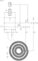
- FIG. 2 is a block diagram showing a wireless power receiving apparatus and a wireless power transmitting apparatus, wherein the power receiving apparatus comprises first and second coils.
- FIGS. 3 and 4 respectively show examples of arrangements of first receiving coils and second receiving coils.
- FIG. 5 shows flow of induced current generated based on a first receiving coil electrically separated from a second receiving coil.
- FIG. 6 shows flow of induced current based on the first receiving coils electrically connected to a second receiving coil.
- FIG. 7 is a circuit diagram showing current induced into a first receiving coil provided to a processor.
- FIG. 8 is a circuit diagram showing currents induced into a first receiving coil and a second receiving coil provided to a processor.
- FIG. 9 shows connection relationships between receiving coils and circuits, in arrangement of each of a first receiving coil and a second receiving coil shown in FIG. 4 .
- FIG. 10 shows a connection relationship between each of receiving coils and a circuit when three receiving coils are arranged.
- a wireless power receiving apparatus 100 may be aligned with a wireless power transmitting apparatus 200 to be operated. More specifically, the wireless power receiving apparatus 100 and the wireless power transmitter 200 may be aligned so that receiving coils (e.g., a first receiving coil 110 and/or a second receiving coil 120) in the wireless power receiving apparatus 100 are disposed on a transmitting coil 210 in the wireless power transmitting apparatus 200, and thus, the receiving coil may be magnetically coupled to the transmitting coil 210.
- receiving coils e.g., a first receiving coil 110 and/or a second receiving coil 120
- a controller 220 in the wireless power transmitting apparatus 200 may control an inverter to control an amount of current flowing through the transmitting coil 210, thereby adjusting the amount of power provided to the wireless power receiving apparatus 100.
- the controller 220 may apply, based on the receiving coil magnetically coupled to the transmitting coil 210, a current to the transmitting coil 210 and a magnetic field may occur in the transmitting coil 210 based on a magnitude of applied current.
- the current may be induced into the receiving coil based on the intensity of the magnetic field generated by the transmitting coil 210 and the current induced into the receiving coil may be provided to batteries or various kinds of loads connected to the wireless power receiving apparatus 100.
- the amount of power that may be provided from the wireless power transmitting apparatus 200 to the wireless power receiving apparatus 100 may be limited based on the fixed size of the receiving coil.
- the intensity of magnetic field generated by the transmitting coil 210 may increase based on the size of the transmitting coil 210 increasing based on changes in the wireless power transmitting apparatus 200 itself or the amount of current flowing through the transmitting coil 210 increasing under the control of the controller 220 of the wireless power transmitting apparatus 200. Based on limiting the size of the receiving coil to a predetermined size, even when the intensity of magnetic field generated by the transmitting coil 210 increases, an amount of interlinkage of magnetic field with respect to the receiving coil is limited to the size of the receiving coil, thereby limiting the amount of power provided to the wireless power receiving apparatus 100.
- the limitation causes a decrease in power transmission efficiency between the wireless power transmitting apparatus 200 and the wireless power receiving apparatus 100.
- the present disclosure provides a wireless power receiving apparatus 100 that includes a plurality of receiving coils to improve the power transmission efficiency and may receive the multi-level power by selectively connecting the plurality of receiving coils to one another.
- the wireless power receiving apparatus 100 may include a first receiving coil 110, a second receiving coil 120, a switch 130, and a processor 140.
- FIG. 2 shows the wireless power receiving apparatus 100, and components of the wireless power receiving apparatus 100 are not limited to an example shown in FIG. 2 . Some components may be added, changed, or deleted as necessary.
- Induction current may be generated by the first receiving coil 110 through electromagnetic induction.
- an induced current may be generated by the first receiving coil 110 based on a magnetic field generated by the transmitter coil 210.
- the first receiving coil 110 may be or may include a flat coil and may be wound clockwise or counterclockwise. Connection terminals for electrical connection with the processor 140 described below may be provided at both ends of the first receiving coil 110.
- the second receiving coil 120 may be electrically connected in series with the first receiving coil 110 by a switch 130.
- first receiving coil 110 and the second receiving coil 120 may be electrically connected or electrically separated through the switch 130, and the switch 130 may be controlled by the processor 140 described below.
- the second receiving coil 120 may be or include a flat coil, and may be wound clockwise or counterclockwise, and connection terminals may be provided at both ends of the second receiving coil 120, respectively, for electrical connection between the first receiving coil 100 and the processor 140.
- the first receiving coil 110 may have one end and the other end of the first receiving coil 110 connected to the processor 140 through each connection terminals to form a closed circuit through which induced current may flow, when the switch 130 is in an off-state.
- the second receiving coil 120 has one end of the second receiving coil 120 connected to one end of the first receiving coil 110 and the other end of the second receiving coil 120 connected to the processor 140 through connection terminals, to form a closed circuit in which the induced current may flow when the switch 130 is in an on-state.
- first receiving coil 110 and the second receiving coil and 120 The arrangement of the first receiving coil 110 and the second receiving coil and 120 is described below in detail with reference to FIGS. 3 and 4 . To this end, connection relationship between receiving coils 110 and 120 and the processor 140 is omitted, in FIGS. 3 and 4 .
- a center of the first receiving coil 110 and a center of the second receiving coil 120 may be the same.
- the first receiving coil 110 and the second receiving coil 120 may have rectangular shapes.
- a center point of the first receiving coil 110 and a center point of the second receiving coil 120 may be the same.
- the center point may represent a center of gravity of each of receiving coils 110 and 120, or may represent the center of each of receiving coils 110 and 120.
- the first receiving coil 110 and the second receiving coil 120 may have circular or elliptical shapes.
- the center point (a point indicating the center of a circle or an ellipse) of the first receiving coil 110 and the center point (a point indicating the center of a circle or an ellipse) of the second receiving coil 120 may be the same.
- the magnetic field generated by a flat transmitting coil 210 may be evenly interlinked to the first receiving coil 110 and/or the second receiving coil 120 based on a distance from the center of the first receiving coil 110 and the second receiving coil 120, thereby improving the uniformity in the power transmission.
- the first receiving coil 110 may be disposed in an inner area of the second receiving coil 120.
- the first receiving coil 110 and the second receiving coil 120 may have a rectangular ring shape having outer edges 112 and 122 and inner edges 111 and 121.
- the inner areas of receiving coils 110 and 120 may be surrounded by the inner edges 111 and 121 of the receiving coils 110 and 120, respectively.
- the first receiving coil 110 may be disposed in an area surrounded by the inner edge 121 of the second receiving coil 120.
- the first receiving coil 110 may be disposed such that an area surrounded by the outer edge 112 is included in an area surrounded by the inner edge 121 of the second receiving coil 120.
- the distance from the center point of the first receiving coil 110 to the outer edge 112 of the first receiving coil 110 may be less than the distance from the center point of the second receiving coil 120 to the inner edge 121 of the second receiving coil 120.
- the first receiving coil 110 and the second receiving coil 120 may be circular flat coils having the same center.
- the outer diameter of the first receiving coil 110 may be less than the inner diameter of the second receiving coil 120.
- the outer diameter of the first receiving coil 110 may correspond to a distance between two points.
- the two points may be provided in a line having a center point of the first receiving coil 110 and extending with respect to the center point of the first receiving coil 110 and connecting a point of the outer edge 112 and a point of the outer edge 122.
- the inner diameter of the second receiving coil 120 may correspond to a distance between two points.
- the two points may be provided in a line having a center point of the second receiving coil 120 and extending with respect to the center point of the second receiving coil 120 and connecting a point of the inner edge 111 and a point of the inner edge 121.
- an outer diameter of the first receiving coil 110 may be D1, and an inner diameter of the second receiving coil 120 may be D2. At this time, the inner diameter D2 may be greater than the outer diameter D1. Accordingly, the first receiving coil 110 may be disposed in the inner area of the second receiving coil 120.
- the first receiving coil 110 may be disposed in the inner area of the second receiving coil 120 so that the multi-level power may be received without expanding the area where the receiving coil is disposed, thereby reducing areas of apparatuses and making apparatuses smaller in size.
- the current may be induced into the first receiving coil 110.
- the first receiving coil 110 is only electrically connected to the processor 140 to form a closed circuit. Accordingly, no current is induced into the second receiving coil 120, but current may be induced only into the first receiving coil 110.
- the switch 130 when the switch 130 is controlled to be turned on so that the first receiving coil 110 and the second receiving coil 120 are electrically connected to each other, the first receiving coil 110 and the second receiving coil 120 may be electrically connected to the processor 140 form a closed circuit. Accordingly, based on operating the first receiving coil 110 and the second receiving coil 120 as one coil, current may be induced into the first receiving coil 110 and the second receiving coil 120.
- the receiving coils 110 and 120 may be connected to resonance capacitors C1 and C2, respectively, and a resonance frequency may be determined based on inductance of each of receiving coils 110 and 120 and capacitance of each of resonance capacitors C1 and C2.
- the first receiving coil 110 may be connected in series with the first resonance capacitor C1, and the resonance frequency of the circuit including the two elements may be determined based on the inductance of the first receiving coil 110 and the capacitance of the first resonance capacitor C1.
- the second receiving coil 120 may be connected in series with the second resonance capacitor C2, and the resonance frequency of the circuit including the two elements may be determined based on the inductance of the second receiving coil 120 and the capacitance of the second resonance capacitor C2.
- the first receiving coil 110 and the first resonance capacitor C1 are connected to each other in series to form a first resonance circuit, which corresponds to a closed circuit.
- the resonance frequency of the first resonance circuit may be determined based on a value in which the inductance of the first receiving coil 110 is multiplied by the capacitance of the first resonance capacitor C1.
- the first receiving coil 110 being connected to the second receiving coil 120
- the first receiving coil 110, the second receiving coil 120, and the second resonance capacitor C2 may be connected to each other in series to form a second resonance circuit, which corresponds to a closed circuit.
- the resonance frequency of the second resonance circuit may be determined based on a value obtained by multiplying the capacitance of the second resonance capacitor C2 by the sum of the inductance of the first receiving coil 110 and the inductance of the second receiving coil 120.
- the resonance frequency of the first resonance circuit and the resonance frequency of the second resonance circuit may be the same.
- the receiving coil in the wireless power receiving apparatus 100 may receive power through magnetic coupling with the transmitting coil 210 in the wireless power transmitting apparatus 200 at a specific resonance frequency. Accordingly, the wireless power receiving apparatus 100 may receive power with very high efficiency based on the current having a frequency adjacent to the resonance frequency applied to the transmitting coil 210.
- the first resonance circuit and the second resonance circuit are switched to each other based on the operation of the switch 130.
- the resonance frequency of the first resonance circuit may be required to be identical to the resonance frequency of the second resonance circuit to receive the power with predetermined efficiency regardless of operation of the switch 130.
- the capacitance of the second resonance capacitor C2 may be less than the capacitance of the first resonance capacitor C 1.
- the total inductance of the first resonance circuit shown in FIG. 5 may be determined based on the inductance of the first receiving coil 110, and the total inductance of the second resonance circuit shown in FIG. 6 may be determined based on a sum of the inductance of the first receiving coil 110 and the inductance of the second receiving coil 120.
- the capacitance of the second resonance capacitor C2 may be less than the capacitance of the first resonance capacitor C 1.
- a first receiving coil 110 and a processor 140 are connected through a full-bridge rectifying circuit 150, and the current induced into the first receiving coil 110 may be provided to the processor 140 through full-bridge rectifying circuit 150.
- a full-bridge rectifying circuit 150 may be provided between the first receiving coil 110 and the processor 140. Based on the switch 130 being controlled to be turned off, a current may be induced into the first receiving coil 110, and the induced current may flow through a lower diode of a left leg of the full-bridge rectifying circuit 150, the first receiving coil 110, and an upper diode of a right leg of the full-bridge rectifying circuit 150. As a result, the current induced into the first receiving coil 110 may be full-wave rectified, and the rectified current may be provided to the processor 140.
- the second receiving coil 120 and the processor 140 are connected through a half-bridge rectifying circuit 160.
- the current may be induced into the first receiving coil 110 and the second receiving coil 120 at the same time and may be provided to the processor 140 through any one of legs of the full-bridge rectifying circuit 150 and the half-bridge rectifying circuit 160.
- a half-bridge rectifying circuit 160 may be provided between the second receiving coil 120 and the processor 140. Based on the switch 130 being controlled to be turned on, current is induced into the first receiving coil 110 and the second receiving coil 120, and the induced current may flow along the lower diode of the left leg of the full-bridge rectifying circuit 150, the first receiving coil 110, the second receiving coil 120, and an upper diode of the half-bridge rectifying circuit 160. As a result, currents induced into the first receiving coil 110 and the second receiving coil 120 may be full-wave rectified, and the rectified current may be provided to the processor 140.
- the power is received by combining the full-bridge rectifying circuit 150 and the half-bridge rectifying circuit 160 and the full-bridge rectifying circuit 150 having the number of receiving coils 110 and 120 may not be required, thereby reducing an area where the circuit is provided in the apparatus and reducing production cost of apparatuses.
- the wireless power receiving apparatus 100 may further include a DC link capacitor C DC . Accordingly, the current induced into at least one of the first receiving coil 110 and the second receiving coil 120 may be stored, as a DC link voltage, in the DC link capacitor C DC , and the processor 140 may be driven based on the DC link voltage.
- both the full-bridge rectifying circuit 150 and the half-bridge rectifying circuit 160 may be connected to a DC link capacitor C DC . Accordingly, the induced current rectified through the method described above may be stored in the form of a smoothed voltage in the DC link capacitor C DC .
- the processor 140 may be connected to a DC link capacitor C DC and may be driven by receiving a DC link voltage stored in the DC link capacitor C DC .
- a regulator 170 may be further provided at an output terminal of the DC link capacitor C DC . Accordingly, the DC link voltage may be converted into a drive voltage to drive the processor 140 by a regulator 170, and the processor 140 may be driven based on the drive voltage.
- the processor 140 may preset a drive voltage to be supplied for operation. Generally, this drive voltage may be less than the DC link voltage. Accordingly, the regulator 170 may convert the DC link voltage into the drive voltage having a magnitude, e.g., 3.3[V]. The processor 140 may be connected to the regulator 170 and may be driven by receiving a drive voltage converted by the regulator 170.
- a method of operating the processor 140 is described below in detail with reference to FIGS. 7 to 9 again.
- the processor 140 may be driven based on the induction current generated by the first receiving coil 110, and may control the switch 130 based on the power information included in the induction current to selectively connect the first receiving coil 110 and the second receiving coil 120.
- a current may be induced into the first receiving coil 110 regardless of an on-state/an off-state of the switch 130.
- the induced current may be provided to the processor 140 along the path described with reference to FIGS. 7 and 8 .
- the processor 140 may be driven when the switch 130 is controlled to be turned on and turned off to control operation of the switch 130.
- the induced current generated by the first receiving coil 110 based on the switch 130 controlled to be turned off may be provided to the processor 140.
- the processor 140 may be driven (waken-up) based on the induced current and may identify power information included in the induced current.
- the power information may include information on an amount of power (hereinafter, referred to as "an amount of transmitted power") that may be transmitted by the wireless power transmitting apparatus 200.
- the controller 220 of the wireless power transmitting apparatus 200 may generate a modulated signal including power information, and may apply, to the transmitting coil 210, an alternating current including the generated modulated signal. Accordingly, an induction current including a modulation signal may be generated by the first receiving coil 110, and the processor 140 may identify power information by demodulating the modulation signal in the induction current.
- the wireless power receiving apparatus 100 may further include any sensor capable of sensing the induced current, and the processor 140 may demodulate the modulated signal in the induced current through the sensor.
- the processor 140 may identify the power information through a frequency modulated signal included in the induced current after being driven by the induced current.
- the controller 220 of the wireless power transmitting apparatus 200 may generate a frequency modulated signal (e.g., a frequency-shift keying (FSK) modulated signal) including power information. Accordingly, the frequency-modulated AC current may be applied to the transmitting coil 210, and the frequency-modulated AC current may be induced to the first receiving coil 110.
- a frequency modulated signal e.g., a frequency-shift keying (FSK) modulated signal
- FSK frequency-shift keying
- the processor 140 may identify the power information by demodulating the frequency modulated signal included in the induced current after being driven based on the current induced into the first receiving coil 110.
- the processor 140 may control the switch 130 based on the identified power information. More specifically, the processor 140 may control the switch 130 to be turned on or turned off based on the amount of transmitted power included in the power information.
- the processor 140 may change the size of the receiving coil by controlling the switch 130 based on the amount of power transmitted by the wireless power transmitting apparatus 200.
- the switch 130 may be turned off when the processor 140 is not driven. After the wireless power transmitting apparatus 200 and the wireless power receiving apparatus 100 are aligned, based on a current being applied to the transmitting coil 210, a current may be induced into the first receiving coil 110, and the processor 140 may be driven based on the induced current.
- the processor 140 may determine the amount of power transmitted by the wireless power transmitting apparatus 200 based on the induced current. Based on the amount of transmitted power being less than a reference magnitude, the switch 130 may be controlled to be turned off without change. Based on the amount of transmitted power being greater than a predetermined magnitude, the switch 130 may be controlled to be turned on. Based on the amount of transmitted power being less than the predetermined magnitude, the wireless power receiving apparatus 100 may receive the power only through the first receiving coil 110. Based on the amount of transmitted power being greater than the predetermined magnitude, the wireless power receiving apparatus 100 may receive the power through the first receiving coil 110 and the second receiving coil 120.
- the wireless power receiving apparatus 100 may receive power by adjusting the size of the receiving coil to be relatively less. Based on the amount of power transmitted by the wireless power transmitting apparatus 200 being relatively greater, the wireless power receiving apparatus 100 may receive power by adjusting the size of the receiving coil to be relatively greater.
- receiving coils shown in FIG. 10 may be classified into a first receiving coil 110, a 2-1 receiving coil 120a, and a 2-2 receiving coil 120b according to lengths of inner diameters of receiving coils.
- a switch that connects the first receiving coil 110 and the 2-1 receiving coil 120a is referred to as "a first switch 130a”.
- a switch that connects a 2-1 receiving coil 120a and a 2-2 receiving coil 120b is referred to as "a second switch 130b".
- the switch 130a may be turned off when the processor 140 is not driven. After the wireless power transmitting apparatus 200 and the wireless power receiving apparatus 100 are aligned, based on current being applied to the transmitting coil 210, a current is induced into the first receiving coil 110, and the processor 140 may be driven based on the induced current.
- the processor 140 may determine the amount of power transmitted by the wireless power transmitting apparatus 200 based on the induced current. Based on the amount of transmitted power being less than a first reference magnitude, the switch 130a may be controlled to be turned off without change. Based on the amount of transmitted power being identical to or greater than the first reference magnitude, the switch 130a may be controlled to be turned on.
- the wireless power receiving apparatus 100 may receive the power through the first receiving coil 110. Based on the amount of transmitted power being identical to or greater than the first reference magnitude, the wireless power receiving apparatus 100 may receive the power through the first receiving coil 110 and the 2-1 receiving coil 120a.
- the processor 140 may compare the amount of transmitted power with a second reference magnitude, which is greater than the first reference magnitude. Based on the amount of transmitted power being less than the second reference magnitude, the first switch 130a may only be controlled to be turned on. Based on the amount of transmitted power being identical to or greater than the second reference magnitude, the second switch 130b, in addition to the first switch 130a, may be controlled to be turned on.
- the wireless power receiving apparatus 100 may receive the power through the first receiving coil 110 and the 2-1 receiving coil 120a. Based on the amount of transmitted power being identical to or greater than the second reference, the wireless power receiving apparatus 100 may receive the power through the first receiving coil 110, the 2-1 receiving coil 120a, and the 2-2 receiving coil 120b.
- compatibility with the wireless power transmitting apparatus 200 that may adjust the amount of transmitted power or a plurality of wireless power transmitting apparatuses 200 having different amounts of transmitted power or the sizes of the transmitting coils 210 may be provided by receiving the multi-level power.
Description
- The present disclosure relates to a wireless power receiving apparatus capable of receiving multi-level power transmitted by a wireless power transmitting apparatus.
- In related art, one of methods for charging batteries may include a method for supplying terminals. The method for supplying the terminals may include receiving commercial power and converting commercial power into voltage and current suitable for batteries, and supplying power to batteries through charging terminals.
- However, such a method for supplying the terminals may cause a momentary discharge phenomenon, sparks, fire due to potential difference between charging terminals of batteries and power supply terminals of commercial power sources. Accordingly, wireless charging methods using wireless power transmission have been proposed.
- The wireless charging method may be performed by a wireless power transmitting apparatus and a wireless power receiving apparatus, and the power may be transferred from the wireless power transmitting apparatus to the wireless power receiving apparatus through electromagnetic induction between the two apparatuses.
- However, through such a wireless charging method, transmitting coils in the wireless power transmitting apparatuses and receiving coils in the wireless power receiving apparatuses may be self-coupled. When the wireless power transmitting apparatus and the wireless power receiving apparatus are produced separately, the two apparatuses may not be compatible with each other, thereby degrading magnetic coupling between the transmitting coil and the receiving coil for wireless power transmission.
- In order to solve this problem,
KR Patent No. 10-1670128 -
FIG. 1 shows operation of a wireless power receiving apparatus in related art and an extract ofFIG. 1 of the prior art document. - Referring to
FIG. 1 , according to the prior art document, a wireless power receiving apparatus 100' may include areceiver 10, and thereceiver 10 may include a first resonance circuit (e.g., L1 and C1) and a second resonance circuit (e.g., L2 and C2) connected to each other in parallel. Arectifier 20 may rectify current received at thereceiver 10 to be provided to a rechargeable battery 200'. - That is, according to the prior art document, the wireless power receiving apparatus 100' may receive the current through at least one of the first resonance circuit (e.g., L1 and C1) and the second resonance circuit (e.g., L2 and C2) based on resonance frequency of the wireless power transmitting apparatus, thereby improving compatibility with the resonance frequency of the wireless power transmitting apparatus.
- Meanwhile, wireless charging methods have been used for various types of terminals having different sizes and power consumptions of batteries, for example, smart phones, tablets, notebooks, TVs, and the like. Various types of power transmitting apparatuses may transmit power having various types of levels to charge terminals.
- As described above, even according to the prior art document, based on the wireless power transmitting apparatus transmitting power having the same resonance frequency and having different sizes, the wireless power receiving apparatus may not provide compatibility with the wireless power transmitting apparatus.
- For example, when a smart phone (i.e., wireless power receiving apparatus) is charged with a wireless power transmitting apparatus to charge a notebook, an amount of power received at the smart phone may be limited to sizes of receiving coils inside of the smart phone, thereby greatly degrading power transmission efficiency. For this reason, smart phones may not provide compatibility with wireless power transmitting apparatuses for notebook charging.
- As described above, there is a demand for a wireless power receiving apparatus capable of receiving multi-level power due to a difference between the amount of power transmitted by the wireless power transmitting apparatus and the amount of power that may be received at the wireless power receiving apparatus.
-
EP 1 898 510 A1 relates to a secondary-side power receiving circuit of noncontact power supplying equipment. - The invention is specified by the independent claim. Preferred embodiments are defined in the dependent claims.
- The present disclosure provides a wireless power receiving apparatus capable of receiving multi-level power.
- The present disclosure also provides a wireless power receiving apparatus capable of receiving a multi-level power without expanding an area where receiving coils are disposed.
- The present disclosure further provides a wireless power receiving apparatus that receives power by combining a full-bridge rectifying circuit and a half-bridge rectifying circuit.
- The objects of the present disclosure are not limited to the above-mentioned objects, and other objects and advantages of the present disclosure which are not mentioned may be understood by the following description and more clearly understood by the embodiments of the present disclosure. It will also be readily apparent that the objects and the advantages of the present disclosure may be implemented by features described in claims, which solely define the scope of the invention.
- The present disclosure relates to a wireless power receiving apparatus receiving multi-level power, as defined in the independent claim 1.
- Preferably, a center of the first receiving coil and a center of the second receiving coil are the same or substantially the same.
- Preferably, the first receiving coil is disposed within an inner area of the second receiving coil.
- Preferably, the first receiving coil and the second receiving coil have substantially circular or rectangular shapes having the same center, and an outer diameter of the first receiving coil is less than an inner diameter of the second receiving coil.
- Preferably, current is induced into the first receiving coil when the first receiving coil is electrically separated from the second receiving coil by the switch, or wherein current is induced into the first receiving coil and the second receiving coil when the first receiving coil is electrically connected to the second receiving coil by the switch.
- Preferably, a resonance frequency of the first resonance circuit and a resonance frequency of the second resonance circuit are the same or substantially the same.
- Preferably, a capacitance of the second resonance capacitor is less than a capacitance of the first resonance capacitor.
- Preferably, the first receiving coil and the processor are connected through a full-bridge rectifying circuit, and a current induced into the first receiving coil is provided to the processor through a full-bridge rectifying circuit.
- Preferably, the second receiving coil and the processor are connected through a half-bridge rectifying circuit, and current induced into both the first receiving coil and the second receiving coil is provided to the processor through any one of legs of the full-bridge rectifying circuit and the half-bridge rectifying circuit.
- Preferably, the wireless power receiving apparatus further comprising a DC link capacitor, wherein a current induced into at least one of the first receiving coil and the second receiving coil is stored as a DC link voltage in the DC link capacitor, and the processor is driven based on the DC link voltage.
- Preferably, the wireless power receiving apparatus further comprising a regulator, wherein the DC link voltage is converted into a drive voltage by the regulator, and the processor is driven based on the drive voltage.
- Preferably, the processor is configured to identify the power information based on a frequency modulated signal included in the induction current after the processor is driven based on the induction current.
- Preferably, the processor is configured to determine an amount of transmitted power based on the power information, and wherein in response to the amount of transmitted power being less than a reference magnitude, the processor is configured to control the switch to be turned off to electrically disconnect the first and second receiving coils from each other, and in response to the amount of transmitted power being equal to greater than the reference magnitude, the processor is configured to control the switch to be turned on to electrically connect the first and second receiving coils to each other.
- According to the present disclosure, a multi-level power may be received by electrically connecting two receiving coils in series or electrically separating two receiving coils from each other based on an amount of power transmitted by the wireless power transmitting apparatus.
- Further, according to the present disclosure, by placing one of the two receiving coils electrically connected or electrically separated based on the amount of power transmitted by the wireless power transmitting apparatus in an inner area of the other receiving coil, the multi-level power may be received without expanding the area where the receiving coils are disposed.
- Further, according to the present disclosure, the full-bridge rectifying circuit may be connected to an output end of any one of two receiving coils and the half-bridge rectifying circuit may be connected to the output of the other one of two receiving coils, so that the power may be received in combination of a full-bridge rectifying circuit and a half-bridge rectifying circuit based on current being induced into the two receiving coils.
- According to the present disclosure, compatibility with the wireless power transmitting apparatus that may adjust an amount of transmitted power or a plurality of wireless power transmitting apparatuses having different amounts of transmitted power or sizes of transmitting coils may be provided by receiving the multi-level power.
- Further, according to the present disclosure, the multi-level power may be received without expanding the area where the receiving coils are disposed, thereby reducing an area of the apparatus and making apparatuses larger in size.
- Further, according to the present disclosure, power may be received by combining a full-bridge rectifying circuit and a half-bridge rectifying circuit, thereby eliminating a need for a full-bridge rectifying circuit having the number of receiving coils, to reduce an area where the circuit is disposed, in the apparatus and to reduce production cost of apparatuses.
- A specific effect of the present disclosure, further to the above-mentioned effect, is described together while describing specific matters to implement the present disclosure.
-
-
FIG. 1 shows operation of a wireless power receiving apparatus in related art. -
FIG. 2 is a block diagram showing a wireless power receiving apparatus and a wireless power transmitting apparatus wherein the power receiving apparatus comprises first and second coils. -
FIGS. 3 and4 respectively show example arrangements of first receiving coils and second receiving coils. -
FIG. 5 shows flow of induced current generated based on a first working coil electrically separated from a second receiving coil. -
FIG. 6 shows flow of induced current generated based on a first receiving coil electrically connected to a second receiving coil. -
FIG. 7 is a circuit diagram showing a current induced into a first receiving coil provided to a processor. -
FIG. 8 is a circuit diagram showing currents induced into a first receiving coil and a second receiving coil provided to a processor. -
FIG. 9 shows connection relationship between receiving coils and circuits, in arrangement of the first receiving coil and the second receiving coil shown inFIG. 4 . -
FIG. 10 shows connection relationship between receiving coils and circuits when three receiving coils are disposed. - The above-mentioned objects, features, and advantages of the present disclosure are described in detail with reference to the accompanying drawings. Accordingly, the skilled person in the art to which the present disclosure pertains may easily implement the technical idea of the present disclosure. In the description of the present disclosure, if it is determined that a detailed description of a well-known relevant technology of the present disclosure may unnecessarily obscure the gist of the present disclosure, the detailed description thereof is omitted. Preferred embodiments of the present disclosure are described in detail with reference to the accompanying drawings. In the drawings, same reference numerals are used to refer to same or similar components.
- It will be understood that, although the terms "first", "second", and the like may be used herein to describe various components, however, these components should not be limited by these terms. These terms are only used to distinguish one component from another component. Thus, a first component may be a second component unless otherwise stated.
- Hereinafter, when any component is arranged in "an upper portion (or a lower portion)" of the component or "on (or under") of the component, any component may be arranged in contact with an upper surface (or a lower surface) of the component, and another component may be interposed between the component and any component arranged on (or under) the component.
- Further, when one component is described as being "connected", "coupled", or "connected" to another component, the component may be directly connected or able to be connected to the other component; however, it is also to be understood that an additional component may be "interposed" between the two components, or the two components may be "connected", "coupled" or "connected" through an additional component.
- Unless otherwise stated, each component may be singular or plural throughout the disclosure.
- As used herein, the singular forms "a," "an" and "the" are intended to include the plural forms as well, unless the context clearly indicates otherwise. In the present disclosure, it should not be construed that terms such as "including" or "comprising" necessarily include various types of components or various steps described in the present disclosure, and it should be construed terms such as "including" or "comprising" do not include some components or some steps or may include additional components or steps.
- In the present disclosure, unless otherwise stated, "A and/or B" means A, B or A and B.
- The present disclosure relates to a multi-level power compatible wireless power receiving apparatus, and more particularly, to a wireless power receiving apparatus capable of receiving multi-level power transmitted by a wireless power transmitting apparatus.
- The wireless power receiving apparatus according to an embodiment of the present disclosure is described below in detail with reference to
FIGS. 2 to 9 . -
FIG. 2 is a block diagram showing a wireless power receiving apparatus and a wireless power transmitting apparatus, wherein the power receiving apparatus comprises first and second coils. -
FIGS. 3 and4 respectively show examples of arrangements of first receiving coils and second receiving coils. -
FIG. 5 shows flow of induced current generated based on a first receiving coil electrically separated from a second receiving coil.FIG. 6 shows flow of induced current based on the first receiving coils electrically connected to a second receiving coil. -
FIG. 7 is a circuit diagram showing current induced into a first receiving coil provided to a processor.FIG. 8 is a circuit diagram showing currents induced into a first receiving coil and a second receiving coil provided to a processor. -
FIG. 9 shows connection relationships between receiving coils and circuits, in arrangement of each of a first receiving coil and a second receiving coil shown inFIG. 4 .FIG. 10 shows a connection relationship between each of receiving coils and a circuit when three receiving coils are arranged. - Referring to
FIG. 2 , a wirelesspower receiving apparatus 100 may be aligned with a wirelesspower transmitting apparatus 200 to be operated. More specifically, the wirelesspower receiving apparatus 100 and thewireless power transmitter 200 may be aligned so that receiving coils (e.g., afirst receiving coil 110 and/or a second receiving coil 120) in the wirelesspower receiving apparatus 100 are disposed on a transmittingcoil 210 in the wirelesspower transmitting apparatus 200, and thus, the receiving coil may be magnetically coupled to the transmittingcoil 210. - Meanwhile, a
controller 220 in the wirelesspower transmitting apparatus 200 may control an inverter to control an amount of current flowing through the transmittingcoil 210, thereby adjusting the amount of power provided to the wirelesspower receiving apparatus 100. - More specifically, the
controller 220 may apply, based on the receiving coil magnetically coupled to the transmittingcoil 210, a current to the transmittingcoil 210 and a magnetic field may occur in the transmittingcoil 210 based on a magnitude of applied current. The current may be induced into the receiving coil based on the intensity of the magnetic field generated by the transmittingcoil 210 and the current induced into the receiving coil may be provided to batteries or various kinds of loads connected to the wirelesspower receiving apparatus 100. - In the method for transmitting the wireless power using the electromagnetic induction phenomenon, the amount of power that may be provided from the wireless
power transmitting apparatus 200 to the wirelesspower receiving apparatus 100 may be limited based on the fixed size of the receiving coil. - More specifically, the intensity of magnetic field generated by the transmitting
coil 210 may increase based on the size of the transmittingcoil 210 increasing based on changes in the wirelesspower transmitting apparatus 200 itself or the amount of current flowing through the transmittingcoil 210 increasing under the control of thecontroller 220 of the wirelesspower transmitting apparatus 200. Based on limiting the size of the receiving coil to a predetermined size, even when the intensity of magnetic field generated by the transmittingcoil 210 increases, an amount of interlinkage of magnetic field with respect to the receiving coil is limited to the size of the receiving coil, thereby limiting the amount of power provided to the wirelesspower receiving apparatus 100. - The limitation causes a decrease in power transmission efficiency between the wireless
power transmitting apparatus 200 and the wirelesspower receiving apparatus 100. The present disclosure provides a wirelesspower receiving apparatus 100 that includes a plurality of receiving coils to improve the power transmission efficiency and may receive the multi-level power by selectively connecting the plurality of receiving coils to one another. - Referring back to
FIG. 2 , the wirelesspower receiving apparatus 100 may include afirst receiving coil 110, asecond receiving coil 120, aswitch 130, and aprocessor 140. In one embodiment,FIG. 2 shows the wirelesspower receiving apparatus 100, and components of the wirelesspower receiving apparatus 100 are not limited to an example shown inFIG. 2 . Some components may be added, changed, or deleted as necessary. - Induction current may be generated by the
first receiving coil 110 through electromagnetic induction. - More specifically, based on the wireless
power transmitting apparatus 200 and the wirelesspower receiving apparatus 100 being aligned, an induced current may be generated by thefirst receiving coil 110 based on a magnetic field generated by thetransmitter coil 210. - The
first receiving coil 110 may be or may include a flat coil and may be wound clockwise or counterclockwise. Connection terminals for electrical connection with theprocessor 140 described below may be provided at both ends of thefirst receiving coil 110. - The
second receiving coil 120 may be electrically connected in series with thefirst receiving coil 110 by aswitch 130. - More specifically, the
first receiving coil 110 and thesecond receiving coil 120 may be electrically connected or electrically separated through theswitch 130, and theswitch 130 may be controlled by theprocessor 140 described below. - Similar to the
first receiving coil 110, thesecond receiving coil 120 may be or include a flat coil, and may be wound clockwise or counterclockwise, and connection terminals may be provided at both ends of thesecond receiving coil 120, respectively, for electrical connection between thefirst receiving coil 100 and theprocessor 140. - As a result, the
first receiving coil 110 may have one end and the other end of thefirst receiving coil 110 connected to theprocessor 140 through each connection terminals to form a closed circuit through which induced current may flow, when theswitch 130 is in an off-state. Further, thesecond receiving coil 120 has one end of thesecond receiving coil 120 connected to one end of thefirst receiving coil 110 and the other end of thesecond receiving coil 120 connected to theprocessor 140 through connection terminals, to form a closed circuit in which the induced current may flow when theswitch 130 is in an on-state. - The arrangement of the
first receiving coil 110 and the second receiving coil and 120 is described below in detail with reference toFIGS. 3 and4 . To this end, connection relationship between receivingcoils processor 140 is omitted, inFIGS. 3 and4 . - A center of the
first receiving coil 110 and a center of thesecond receiving coil 120 may be the same. - For example, referring to
FIG. 3 , thefirst receiving coil 110 and thesecond receiving coil 120 may have rectangular shapes. At this time, a center point of thefirst receiving coil 110 and a center point of thesecond receiving coil 120 may be the same. The center point may represent a center of gravity of each of receivingcoils coils - In another example, referring to
FIG. 4 , thefirst receiving coil 110 and thesecond receiving coil 120 may have circular or elliptical shapes. At this time, the center point (a point indicating the center of a circle or an ellipse) of thefirst receiving coil 110 and the center point (a point indicating the center of a circle or an ellipse) of thesecond receiving coil 120 may be the same. - As the center of the
first receiving coil 110 and the center of thesecond receiving coil 120 are the same, the magnetic field generated by aflat transmitting coil 210 may be evenly interlinked to thefirst receiving coil 110 and/or thesecond receiving coil 120 based on a distance from the center of thefirst receiving coil 110 and thesecond receiving coil 120, thereby improving the uniformity in the power transmission. - Meanwhile, the
first receiving coil 110 may be disposed in an inner area of thesecond receiving coil 120. - Referring back to
FIG. 3 , for example, thefirst receiving coil 110 and thesecond receiving coil 120 may have a rectangular ring shape havingouter edges inner edges coils inner edges coils - The
first receiving coil 110 may be disposed in an area surrounded by theinner edge 121 of thesecond receiving coil 120. In other words, thefirst receiving coil 110 may be disposed such that an area surrounded by theouter edge 112 is included in an area surrounded by theinner edge 121 of thesecond receiving coil 120. To this end, the distance from the center point of thefirst receiving coil 110 to theouter edge 112 of thefirst receiving coil 110 may be less than the distance from the center point of thesecond receiving coil 120 to theinner edge 121 of thesecond receiving coil 120. - In another example, referring back to
FIG. 4 , thefirst receiving coil 110 and thesecond receiving coil 120 may be circular flat coils having the same center. The outer diameter of thefirst receiving coil 110 may be less than the inner diameter of thesecond receiving coil 120. The outer diameter of thefirst receiving coil 110 may correspond to a distance between two points. The two points may be provided in a line having a center point of thefirst receiving coil 110 and extending with respect to the center point of thefirst receiving coil 110 and connecting a point of theouter edge 112 and a point of theouter edge 122. The inner diameter of thesecond receiving coil 120 may correspond to a distance between two points. The two points may be provided in a line having a center point of thesecond receiving coil 120 and extending with respect to the center point of thesecond receiving coil 120 and connecting a point of theinner edge 111 and a point of theinner edge 121. - As shown in
FIG. 4 , an outer diameter of thefirst receiving coil 110 may be D1, and an inner diameter of thesecond receiving coil 120 may be D2. At this time, the inner diameter D2 may be greater than the outer diameter D1. Accordingly, thefirst receiving coil 110 may be disposed in the inner area of thesecond receiving coil 120. - According to the present disclosure, the
first receiving coil 110 may be disposed in the inner area of thesecond receiving coil 120 so that the multi-level power may be received without expanding the area where the receiving coil is disposed, thereby reducing areas of apparatuses and making apparatuses smaller in size. - Meanwhile, as described above, as the
first receiving coil 110 forms a closed circuit regardless of the operation of theswitch 130, based on thefirst receiving coil 110 being electrically separated from thesecond receiving coil 120 by the switch, the current may be induced into thefirst receiving coil 110. - Referring to
FIG. 5 , based on theswitch 130 being controlled to be turned off to electrically separate thefirst receiving coil 110 from thesecond receiving coil 120, thefirst receiving coil 110 is only electrically connected to theprocessor 140 to form a closed circuit. Accordingly, no current is induced into thesecond receiving coil 120, but current may be induced only into thefirst receiving coil 110. - Meanwhile, based on the
first receiving coil 110 being electrically connected to thesecond receiving coil 120 by theswitch 130, current may be induced into thefirst receiving coil 110 and thesecond receiving coil 120. - Referring to
FIG. 6 , when theswitch 130 is controlled to be turned on so that thefirst receiving coil 110 and thesecond receiving coil 120 are electrically connected to each other, thefirst receiving coil 110 and thesecond receiving coil 120 may be electrically connected to theprocessor 140 form a closed circuit. Accordingly, based on operating thefirst receiving coil 110 and thesecond receiving coil 120 as one coil, current may be induced into thefirst receiving coil 110 and thesecond receiving coil 120. - Meanwhile, as shown in
FIGS. 5 and6 , the receivingcoils coils - More specifically, the
first receiving coil 110 may be connected in series with the first resonance capacitor C1, and the resonance frequency of the circuit including the two elements may be determined based on the inductance of thefirst receiving coil 110 and the capacitance of the first resonance capacitor C1. Further, thesecond receiving coil 120 may be connected in series with the second resonance capacitor C2, and the resonance frequency of the circuit including the two elements may be determined based on the inductance of thesecond receiving coil 120 and the capacitance of the second resonance capacitor C2. - Referring back to
FIG. 5 , based on thefirst receiving coil 110 electrically separated from thesecond receiving coil 120, thefirst receiving coil 110 and the first resonance capacitor C1 are connected to each other in series to form a first resonance circuit, which corresponds to a closed circuit. At this time, the resonance frequency of the first resonance circuit may be determined based on a value in which the inductance of thefirst receiving coil 110 is multiplied by the capacitance of the first resonance capacitor C1. - Further, referring back to
FIG. 6 , based on thefirst receiving coil 110 being connected to thesecond receiving coil 120, thefirst receiving coil 110, thesecond receiving coil 120, and the second resonance capacitor C2 may be connected to each other in series to form a second resonance circuit, which corresponds to a closed circuit. In this case, the resonance frequency of the second resonance circuit may be determined based on a value obtained by multiplying the capacitance of the second resonance capacitor C2 by the sum of the inductance of thefirst receiving coil 110 and the inductance of thesecond receiving coil 120.. - As described above, based on providing the first resonance circuit and the second resonance circuit, the resonance frequency of the first resonance circuit and the resonance frequency of the second resonance circuit may be the same.
- The receiving coil in the wireless
power receiving apparatus 100 may receive power through magnetic coupling with the transmittingcoil 210 in the wirelesspower transmitting apparatus 200 at a specific resonance frequency. Accordingly, the wirelesspower receiving apparatus 100 may receive power with very high efficiency based on the current having a frequency adjacent to the resonance frequency applied to the transmittingcoil 210. - The first resonance circuit and the second resonance circuit are switched to each other based on the operation of the
switch 130. The resonance frequency of the first resonance circuit may be required to be identical to the resonance frequency of the second resonance circuit to receive the power with predetermined efficiency regardless of operation of theswitch 130. - To this end, the capacitance of the second resonance capacitor C2 may be less than the capacitance of the first resonance capacitor C 1.
- The total inductance of the first resonance circuit shown in
FIG. 5 may be determined based on the inductance of thefirst receiving coil 110, and the total inductance of the second resonance circuit shown inFIG. 6 may be determined based on a sum of the inductance of thefirst receiving coil 110 and the inductance of thesecond receiving coil 120. - Meanwhile, as described above, as the resonance frequency of each resonance circuit is determined based on the product of the total inductance and the total capacitance of each of resonance circuits, in order to set the resonance frequency of the second resonance circuit to be the same as the resonance frequency of the first resonance circuit, the capacitance of the second resonance capacitor C2 may be less than the capacitance of the first resonance capacitor C 1.
- Referring to
FIGS. 7 to 9 , a process is described below in detail in which a current induced into thefirst receiving coil 110 and/or thesecond receiving coil 120 is provided to theprocessor 140. - A
first receiving coil 110 and aprocessor 140 are connected through a full-bridge rectifying circuit 150, and the current induced into thefirst receiving coil 110 may be provided to theprocessor 140 through full-bridge rectifying circuit 150. - Referring to
FIG. 7 , a full-bridge rectifying circuit 150 may be provided between thefirst receiving coil 110 and theprocessor 140. Based on theswitch 130 being controlled to be turned off, a current may be induced into thefirst receiving coil 110, and the induced current may flow through a lower diode of a left leg of the full-bridge rectifying circuit 150, thefirst receiving coil 110, and an upper diode of a right leg of the full-bridge rectifying circuit 150. As a result, the current induced into thefirst receiving coil 110 may be full-wave rectified, and the rectified current may be provided to theprocessor 140. - Meanwhile, the
second receiving coil 120 and theprocessor 140 are connected through a half-bridge rectifying circuit 160. As shown inFIG. 8 , the current may be induced into thefirst receiving coil 110 and thesecond receiving coil 120 at the same time and may be provided to theprocessor 140 through any one of legs of the full-bridge rectifying circuit 150 and the half-bridge rectifying circuit 160. - Referring to
FIG. 8 , a half-bridge rectifying circuit 160 may be provided between thesecond receiving coil 120 and theprocessor 140. Based on theswitch 130 being controlled to be turned on, current is induced into thefirst receiving coil 110 and thesecond receiving coil 120, and the induced current may flow along the lower diode of the left leg of the full-bridge rectifying circuit 150, thefirst receiving coil 110, thesecond receiving coil 120, and an upper diode of the half-bridge rectifying circuit 160. As a result, currents induced into thefirst receiving coil 110 and thesecond receiving coil 120 may be full-wave rectified, and the rectified current may be provided to theprocessor 140. - As described above, according to the present disclosure, the power is received by combining the full-
bridge rectifying circuit 150 and the half-bridge rectifying circuit 160 and the full-bridge rectifying circuit 150 having the number of receivingcoils - Meanwhile, in order to smooth the rectified current, the wireless
power receiving apparatus 100 may further include a DC link capacitor CDC. Accordingly, the current induced into at least one of thefirst receiving coil 110 and thesecond receiving coil 120 may be stored, as a DC link voltage, in the DC link capacitor CDC, and theprocessor 140 may be driven based on the DC link voltage. - Referring back to
FIGS. 7 and8 , both the full-bridge rectifying circuit 150 and the half-bridge rectifying circuit 160 may be connected to a DC link capacitor CDC. Accordingly, the induced current rectified through the method described above may be stored in the form of a smoothed voltage in the DC link capacitor CDC. - The
processor 140 may be connected to a DC link capacitor CDC and may be driven by receiving a DC link voltage stored in the DC link capacitor CDC. - Meanwhile, a
regulator 170 may be further provided at an output terminal of the DC link capacitor CDC. Accordingly, the DC link voltage may be converted into a drive voltage to drive theprocessor 140 by aregulator 170, and theprocessor 140 may be driven based on the drive voltage. - Specifically, the
processor 140 may preset a drive voltage to be supplied for operation. Generally, this drive voltage may be less than the DC link voltage. Accordingly, theregulator 170 may convert the DC link voltage into the drive voltage having a magnitude, e.g., 3.3[V]. Theprocessor 140 may be connected to theregulator 170 and may be driven by receiving a drive voltage converted by theregulator 170. - A method of operating the
processor 140 is described below in detail with reference toFIGS. 7 to 9 again. - The
processor 140 may be driven based on the induction current generated by thefirst receiving coil 110, and may control theswitch 130 based on the power information included in the induction current to selectively connect thefirst receiving coil 110 and thesecond receiving coil 120. - Based on the wireless
power transmitting apparatus 200 aligned with the wirelesspower receiving apparatus 100, a current may be induced into thefirst receiving coil 110 regardless of an on-state/an off-state of theswitch 130. The induced current may be provided to theprocessor 140 along the path described with reference toFIGS. 7 and8 . In other words, theprocessor 140 may be driven when theswitch 130 is controlled to be turned on and turned off to control operation of theswitch 130. - However, a process of controlling the
switch 130 by driving theprocessor 140 based on theswitch 130 controlled to be turned off is described below. - Referring back to
FIG. 7 , the induced current generated by thefirst receiving coil 110 based on theswitch 130 controlled to be turned off may be provided to theprocessor 140. Theprocessor 140 may be driven (waken-up) based on the induced current and may identify power information included in the induced current. In this case, the power information may include information on an amount of power (hereinafter, referred to as "an amount of transmitted power") that may be transmitted by the wirelesspower transmitting apparatus 200. - Specifically, the
controller 220 of the wirelesspower transmitting apparatus 200 may generate a modulated signal including power information, and may apply, to the transmittingcoil 210, an alternating current including the generated modulated signal. Accordingly, an induction current including a modulation signal may be generated by thefirst receiving coil 110, and theprocessor 140 may identify power information by demodulating the modulation signal in the induction current. To this end, the wirelesspower receiving apparatus 100 may further include any sensor capable of sensing the induced current, and theprocessor 140 may demodulate the modulated signal in the induced current through the sensor. - For example, the
processor 140 may identify the power information through a frequency modulated signal included in the induced current after being driven by the induced current. - The
controller 220 of the wirelesspower transmitting apparatus 200 may generate a frequency modulated signal (e.g., a frequency-shift keying (FSK) modulated signal) including power information. Accordingly, the frequency-modulated AC current may be applied to the transmittingcoil 210, and the frequency-modulated AC current may be induced to thefirst receiving coil 110. - The
processor 140 may identify the power information by demodulating the frequency modulated signal included in the induced current after being driven based on the current induced into thefirst receiving coil 110. - The
processor 140 may control theswitch 130 based on the identified power information. More specifically, theprocessor 140 may control theswitch 130 to be turned on or turned off based on the amount of transmitted power included in the power information. - As described above, when the size of the receiving coil is fixed, the amount of power that may be received by the wireless
power receiving apparatus 100 may be limited. Accordingly, theprocessor 140 may change the size of the receiving coil by controlling theswitch 130 based on the amount of power transmitted by the wirelesspower transmitting apparatus 200. - Specifically, referring to
FIG. 9 , theswitch 130 may be turned off when theprocessor 140 is not driven. After the wirelesspower transmitting apparatus 200 and the wirelesspower receiving apparatus 100 are aligned, based on a current being applied to the transmittingcoil 210, a current may be induced into thefirst receiving coil 110, and theprocessor 140 may be driven based on the induced current. - The
processor 140 may determine the amount of power transmitted by the wirelesspower transmitting apparatus 200 based on the induced current. Based on the amount of transmitted power being less than a reference magnitude, theswitch 130 may be controlled to be turned off without change. Based on the amount of transmitted power being greater than a predetermined magnitude, theswitch 130 may be controlled to be turned on. Based on the amount of transmitted power being less than the predetermined magnitude, the wirelesspower receiving apparatus 100 may receive the power only through thefirst receiving coil 110. Based on the amount of transmitted power being greater than the predetermined magnitude, the wirelesspower receiving apparatus 100 may receive the power through thefirst receiving coil 110 and thesecond receiving coil 120. - That is, based on the amount of power transmitted by the wireless
power transmitting apparatus 200 being relatively low, the wirelesspower receiving apparatus 100 may receive power by adjusting the size of the receiving coil to be relatively less. Based on the amount of power transmitted by the wirelesspower transmitting apparatus 200 being relatively greater, the wirelesspower receiving apparatus 100 may receive power by adjusting the size of the receiving coil to be relatively greater. - Further, the operation of the
processor 140 is described in detail with reference toFIG. 10 . - Referring to
FIG. 10 , unlike the above-mentioned matter, three receiving coils in a wirelesspower receiving apparatus 100 may be provided. Hereinafter, receiving coils shown inFIG. 10 may be classified into afirst receiving coil 110, a 2-1receiving coil 120a, and a 2-2receiving coil 120b according to lengths of inner diameters of receiving coils. A switch that connects thefirst receiving coil 110 and the 2-1receiving coil 120a is referred to as "afirst switch 130a". A switch that connects a 2-1receiving coil 120a and a 2-2receiving coil 120b is referred to as "asecond switch 130b". - The
switch 130a may be turned off when theprocessor 140 is not driven. After the wirelesspower transmitting apparatus 200 and the wirelesspower receiving apparatus 100 are aligned, based on current being applied to the transmittingcoil 210, a current is induced into thefirst receiving coil 110, and theprocessor 140 may be driven based on the induced current. - The
processor 140 may determine the amount of power transmitted by the wirelesspower transmitting apparatus 200 based on the induced current. Based on the amount of transmitted power being less than a first reference magnitude, theswitch 130a may be controlled to be turned off without change. Based on the amount of transmitted power being identical to or greater than the first reference magnitude, theswitch 130a may be controlled to be turned on. - Accordingly, based on the amount of transmitted power being less than the first reference magnitude, the wireless
power receiving apparatus 100 may receive the power through thefirst receiving coil 110. Based on the amount of transmitted power being identical to or greater than the first reference magnitude, the wirelesspower receiving apparatus 100 may receive the power through thefirst receiving coil 110 and the 2-1receiving coil 120a. - Further, based on the amount of transmitted power being identical to or greater than the first reference magnitude, the
processor 140 may compare the amount of transmitted power with a second reference magnitude, which is greater than the first reference magnitude. Based on the amount of transmitted power being less than the second reference magnitude, thefirst switch 130a may only be controlled to be turned on. Based on the amount of transmitted power being identical to or greater than the second reference magnitude, thesecond switch 130b, in addition to thefirst switch 130a, may be controlled to be turned on. - Accordingly, based on the amount of transmitted power being identical to or greater than the first reference magnitude and being less than the second reference magnitude, the wireless
power receiving apparatus 100 may receive the power through thefirst receiving coil 110 and the 2-1receiving coil 120a. Based on the amount of transmitted power being identical to or greater than the second reference, the wirelesspower receiving apparatus 100 may receive the power through thefirst receiving coil 110, the 2-1receiving coil 120a, and the 2-2receiving coil 120b. - As described above, according to the present disclosure, compatibility with the wireless
power transmitting apparatus 200 that may adjust the amount of transmitted power or a plurality of wirelesspower transmitting apparatuses 200 having different amounts of transmitted power or the sizes of the transmittingcoils 210 may be provided by receiving the multi-level power.
Claims (13)
- A wireless power receiving apparatus (100), the wireless power receiving apparatus (100) configured to receive multi-level power, comprising:a first receiving coil (110) configured such that induction current is generated based on an electromagnetic induction;a first resonance capacitor (C1) connected to first receiving coil (110);a second receiving coil (120) configured to be selectively connected to the first receiving coil (110) in series, by a switch (130);a second resonance capacitor (C2) connected to second receiving coil (120); anda processor (140) configured to be driven driven based on the induction current generated by the first receiving coil (110), configured to control the switch (130) based on power information included in the induction current, and selectively and electrically connect the first receiving coil (110) and the second receiving coil (120) based on an operation of the switch,characterized in that the first receiving coil (110) and the first resonance capacitor (C1) are configured to form a first resonance circuit, when the first receiving coil (110) is electrically separated from the second receiving coil (120) by the switch (130), andwherein first receiving coil (110), the second receiving coil (120) and the second resonance capacitor (C2) are configured to form a second resonance circuit, when the first receiving coil (110) is electrically connected to the second receiving coil (120) by the switch (130).
- The wireless power receiving apparatus (100) of claim 1, wherein a center of the first receiving coil (110) and a center of the second receiving coil (120) are the same or substantially the same.
- The wireless power receiving apparatus (100) of claim 1 or 2, wherein the first receiving coil (110) is disposed within an inner area of the second receiving coil (120).
- The wireless power receiving apparatus (100) of any one of the preceding claims, wherein the first receiving coil (110) and the second receiving coil (120) have substantially circular or rectangular shapes having the same center, and an outer diameter of the first receiving coil (110) is less than an inner diameter of the second receiving coil (120).
- The wireless power receiving apparatus (100) of any one of the preceding claims, which is configured such that current is induced into the first receiving coil (110) when the first receiving coil (110) is electrically separated from the second receiving coil (120) by the switch (130), or which is configured such that current is induced into the first receiving coil (110) and the second receiving coil (120) when the first receiving coil (110) is electrically connected to the second receiving coil (120) by the switch (130).
- The wireless power receiving apparatus (100) of claim 1, wherein a resonance frequency of the first resonance circuit and a resonance frequency of the second resonance circuit are the same or substantially the same.
- The wireless power receiving apparatus (100) of claim 1 or 6, wherein a capacitance of the second resonance capacitor (C2) is less than a capacitance of the first resonance capacitor (C1).
- The wireless power receiving apparatus (100) of any one of the preceding claims, wherein the first receiving coil (110) and the processor (140) are connected through a full-bridge rectifying circuit (150), and a current induced into the first receiving coil (110) is provided to the processor (140) through a full-bridge rectifying circuit (150).
- The wireless power receiving apparatus (100) of claim 8, wherein the second receiving coil (120) and the processor (140) are connected through a half-bridge rectifying circuit (160), and current induced into both the first receiving coil (110) and the second receiving coil (120) is provided to the processor (140) through any one of legs of the full-bridge rectifying circuit (150) and the half-bridge rectifying circuit (160).
- The wireless power receiving apparatus (100) of any one of the preceding claims, further comprising a DC link capacitor (CDC),
wherein a current induced into at least one of the first receiving coil (110) and the second receiving coil (120) is stored as a DC link voltage in the DC link capacitor (CDC), and the processor (140) is driven based on the DC link voltage. - The wireless power receiving apparatus (100) of claim 10, further comprising a regulator (170),
wherein the DC link voltage is converted into a drive voltage by the regulator (170), and the processor (140) is driven based on the drive voltage. - The wireless power receiving apparatus (100) of any one of the preceding claims, wherein the processor (140) is configured to identify the power information based on a frequency modulated signal included in the induction current after the processor (140) is driven based on the induction current.
- The wireless power receiving apparatus (100) of any one of the preceding claims, wherein the processor (140) is configured to determine an amount of transmitted power based on the power information, andwherein in response to the amount of transmitted power being less than a reference magnitude, the processor (140) is configured to control the switch (130) to be turned off to electrically disconnect the first and second receiving coils (110, 120) from each other, andin response to the amount of transmitted power being equal to greater than the reference magnitude, the processor (140) is configured to control the switch (130) to be turned on to electrically connect the first and second receiving coils (110, 120) to each other.
Applications Claiming Priority (1)
| Application Number | Priority Date | Filing Date | Title |
|---|---|---|---|
| KR1020190111698A KR102261860B1 (en) | 2019-09-09 | 2019-09-09 | Multi-level power compatible wireless power receiving apparatus |
Publications (2)
| Publication Number | Publication Date |
|---|---|
| EP3790161A1 EP3790161A1 (en) | 2021-03-10 |
| EP3790161B1 true EP3790161B1 (en) | 2023-12-06 |
Family
ID=71994343
Family Applications (1)
| Application Number | Title | Priority Date | Filing Date |
|---|---|---|---|
| EP20189784.0A Active EP3790161B1 (en) | 2019-09-09 | 2020-08-06 | Multi-level power compatible wireless power receiving apparatus |
Country Status (3)
| Country | Link |
|---|---|
| US (1) | US11218028B2 (en) |
| EP (1) | EP3790161B1 (en) |
| KR (1) | KR102261860B1 (en) |
Families Citing this family (3)
| Publication number | Priority date | Publication date | Assignee | Title |
|---|---|---|---|---|
| EP3891863A4 (en) * | 2018-12-04 | 2022-10-12 | Powermat Technologies Ltd. | Adaptive wireless power transmitter |
| CN113131628B (en) * | 2021-03-17 | 2023-09-29 | 伏达半导体(合肥)股份有限公司 | Wireless power transmission system, wireless power transmission device and method |
| KR20220163192A (en) * | 2021-06-02 | 2022-12-09 | 삼성전자주식회사 | Wireless power receiver and method performed by wireless power receiver |
Family Cites Families (20)
| Publication number | Priority date | Publication date | Assignee | Title |
|---|---|---|---|---|
| EP1898510A4 (en) | 2005-04-22 | 2017-03-01 | Daifuku Co., Ltd. | Secondary-side power receiving circuit of noncontact power supplying equipment |
| KR101118471B1 (en) | 2009-09-30 | 2012-03-12 | 한국전기연구원 | Spiral Antenna and wireless power transmission device using spiral antenna |
| US10574297B2 (en) * | 2009-11-25 | 2020-02-25 | Triune Ip, Llc | Multi-use wireless power and data system |
| JP5810291B2 (en) * | 2010-03-30 | 2015-11-11 | パナソニックIpマネジメント株式会社 | Wireless power transmission system |
| US20120025623A1 (en) * | 2010-07-28 | 2012-02-02 | Qualcomm Incorporated | Multi-loop wireless power receive coil |
| KR102042685B1 (en) * | 2013-03-14 | 2019-11-11 | 삼성전자주식회사 | Wireless power transmission apparatus and wireless power reception apparatus |
| US10320234B2 (en) * | 2013-08-02 | 2019-06-11 | Integrated Device Technology, Inc. | Multimode wireless power receivers and related methods |
| WO2015140917A1 (en) | 2014-03-18 | 2015-09-24 | 三菱電機エンジニアリング株式会社 | Resonance power transmission apparatus, transmission-side power transmission apparatus, and reception-side power transmission apparatus |
| KR101670128B1 (en) | 2014-04-30 | 2016-10-27 | 삼성전기주식회사 | Wireless power receiver and electronic device comprising the same |
| US9787140B2 (en) * | 2014-11-19 | 2017-10-10 | Te Connectivity Corporation | Wireless power transfer method and circuit |
| KR102272354B1 (en) * | 2014-11-26 | 2021-07-02 | 에스엘 주식회사 | Apparatus for wireless power transmission |
| KR20160123932A (en) * | 2015-04-16 | 2016-10-26 | 삼성전기주식회사 | A wireless power receiving device, a coil module for the same, and an apparatus comprising the same |
| US9960628B2 (en) * | 2015-08-07 | 2018-05-01 | Nucurrent, Inc. | Single structure multi mode antenna having a single layer structure with coils on opposing sides for wireless power transmission using magnetic field coupling |
| US11223236B2 (en) | 2016-02-24 | 2022-01-11 | Koninklijke Philips N.V. | Wireless inductive power transfer |
| JP6510455B2 (en) * | 2016-03-30 | 2019-05-08 | 矢崎総業株式会社 | Contactless power transmission device |
| US10523035B2 (en) * | 2016-07-11 | 2019-12-31 | Motorola Mobility Llc | Multi-tapped coil for wireless charging range and efficiency |
| US10680466B2 (en) * | 2017-03-17 | 2020-06-09 | Integrated Device Technology, Inc. | Circuits and systems for wireless power transmission |
| KR102433977B1 (en) * | 2017-10-31 | 2022-08-22 | 한국전자통신연구원 | Wireless power receiving apparatus controlling output voltage |
| CN111566894B (en) * | 2018-05-25 | 2023-06-02 | Oppo广东移动通信有限公司 | Wireless charging receiving device and mobile terminal |
| CN111566889B (en) * | 2018-05-25 | 2024-02-02 | Oppo广东移动通信有限公司 | Wireless charging receiving device and mobile terminal |
-
2019
- 2019-09-09 KR KR1020190111698A patent/KR102261860B1/en active IP Right Grant
-
2020
- 2020-01-10 US US16/739,749 patent/US11218028B2/en active Active
- 2020-08-06 EP EP20189784.0A patent/EP3790161B1/en active Active
Also Published As
| Publication number | Publication date |
|---|---|
| KR20210030131A (en) | 2021-03-17 |
| KR102261860B1 (en) | 2021-06-07 |
| US11218028B2 (en) | 2022-01-04 |
| US20210075270A1 (en) | 2021-03-11 |
| EP3790161A1 (en) | 2021-03-10 |
Similar Documents
| Publication | Publication Date | Title |
|---|---|---|
| US11936202B2 (en) | Hybrid wireless power transmitting system and method therefor | |
| EP3790161B1 (en) | Multi-level power compatible wireless power receiving apparatus | |
| US10819150B2 (en) | Non-contact electric power feeding system, terminal device, non-contact electric power feeding device, and non-contact electric power feeding method | |
| JP6591851B2 (en) | Wireless power transfer apparatus and method | |
| US9423439B2 (en) | Apparatus and method for detecting foreign object in wireless power transmitting system | |
| CN107222039B (en) | Wireless power transmission system | |
| US10224761B2 (en) | Method for controlling power in a wireless power transmission apparatus and a wireless power transmission apparatus | |
| KR20150109722A (en) | Method and apparatus for transmitting power wirelessly | |
| WO2012092183A2 (en) | System for wireless power transmission | |
| US9893568B2 (en) | Wireless power transmitter, control circuit and control method thereof, and charger | |
| KR102491037B1 (en) | Wireless power reception device and wireless communication method | |
| US20230065766A1 (en) | Electronic Device, Wireless Charging Receive Apparatus, Control Method, and Wireless Charging System | |
| US9876363B2 (en) | Non-contact type power transmitting apparatus, non-contact type power transmitting-receiving apparatus, contact/non-contact type power transmitting apparatus, and contact/non-contact type power transmitting-receiving apparatus | |
| CN113726028B (en) | Electronic equipment and control method thereof | |
| WO2016167123A1 (en) | Power reception device, power reception method and power supply system | |
| KR101996966B1 (en) | Wireless Power Transfer System and Operating method thereof | |
| CN111262348B (en) | Control method and device of wireless charging device and wireless charging device | |
| KR102427343B1 (en) | Wireless charger | |
| US9106088B2 (en) | Non-contact power transmission apparatus | |
| WO2017130422A1 (en) | Magnetic resonance-type power supply system |
Legal Events
| Date | Code | Title | Description |
|---|---|---|---|
| PUAI | Public reference made under article 153(3) epc to a published international application that has entered the european phase |
Free format text: ORIGINAL CODE: 0009012 |
|
| STAA | Information on the status of an ep patent application or granted ep patent |
Free format text: STATUS: THE APPLICATION HAS BEEN PUBLISHED |
|
| AK | Designated contracting states |
Kind code of ref document: A1 Designated state(s): AL AT BE BG CH CY CZ DE DK EE ES FI FR GB GR HR HU IE IS IT LI LT LU LV MC MK MT NL NO PL PT RO RS SE SI SK SM TR |
|
| AX | Request for extension of the european patent |
Extension state: BA ME |
|
| STAA | Information on the status of an ep patent application or granted ep patent |
Free format text: STATUS: REQUEST FOR EXAMINATION WAS MADE |
|
| 17P | Request for examination filed |
Effective date: 20210910 |
|
| RBV | Designated contracting states (corrected) |
Designated state(s): AL AT BE BG CH CY CZ DE DK EE ES FI FR GB GR HR HU IE IS IT LI LT LU LV MC MK MT NL NO PL PT RO RS SE SI SK SM TR |
|
| RIC1 | Information provided on ipc code assigned before grant |
Ipc: H02J 50/00 20160101ALI20230504BHEP Ipc: H02J 50/12 20160101ALI20230504BHEP Ipc: H02J 50/40 20160101AFI20230504BHEP |
|
| GRAP | Despatch of communication of intention to grant a patent |
Free format text: ORIGINAL CODE: EPIDOSNIGR1 |
|
| STAA | Information on the status of an ep patent application or granted ep patent |
Free format text: STATUS: GRANT OF PATENT IS INTENDED |
|
| INTG | Intention to grant announced |
Effective date: 20230619 |
|
| GRAS | Grant fee paid |
Free format text: ORIGINAL CODE: EPIDOSNIGR3 |
|
| GRAA | (expected) grant |
Free format text: ORIGINAL CODE: 0009210 |
|
| STAA | Information on the status of an ep patent application or granted ep patent |
Free format text: STATUS: THE PATENT HAS BEEN GRANTED |
|
| AK | Designated contracting states |
Kind code of ref document: B1 Designated state(s): AL AT BE BG CH CY CZ DE DK EE ES FI FR GB GR HR HU IE IS IT LI LT LU LV MC MK MT NL NO PL PT RO RS SE SI SK SM TR |
|
| REG | Reference to a national code |
Ref country code: GB Ref legal event code: FG4D |
|
| REG | Reference to a national code |
Ref country code: DE Ref legal event code: R096 Ref document number: 602020022202 Country of ref document: DE |
|
| REG | Reference to a national code |
Ref country code: CH Ref legal event code: EP |
|
| REG | Reference to a national code |
Ref country code: IE Ref legal event code: FG4D |
|
| REG | Reference to a national code |
Ref country code: LT Ref legal event code: MG9D |
|
| PG25 | Lapsed in a contracting state [announced via postgrant information from national office to epo] |
Ref country code: GR Free format text: LAPSE BECAUSE OF FAILURE TO SUBMIT A TRANSLATION OF THE DESCRIPTION OR TO PAY THE FEE WITHIN THE PRESCRIBED TIME-LIMIT Effective date: 20240307 |