EP3789863A1 - Electromagnetic film wire-out structure, direct-type backlight display module and display - Google Patents
Electromagnetic film wire-out structure, direct-type backlight display module and display Download PDFInfo
- Publication number
- EP3789863A1 EP3789863A1 EP18917349.5A EP18917349A EP3789863A1 EP 3789863 A1 EP3789863 A1 EP 3789863A1 EP 18917349 A EP18917349 A EP 18917349A EP 3789863 A1 EP3789863 A1 EP 3789863A1
- Authority
- EP
- European Patent Office
- Prior art keywords
- electromagnetic
- backplate
- film
- circuit board
- flexible
- Prior art date
- Legal status (The legal status is an assumption and is not a legal conclusion. Google has not performed a legal analysis and makes no representation as to the accuracy of the status listed.)
- Granted
Links
Images
Classifications
-
- G—PHYSICS
- G06—COMPUTING OR CALCULATING; COUNTING
- G06F—ELECTRIC DIGITAL DATA PROCESSING
- G06F3/00—Input arrangements for transferring data to be processed into a form capable of being handled by the computer; Output arrangements for transferring data from processing unit to output unit, e.g. interface arrangements
- G06F3/01—Input arrangements or combined input and output arrangements for interaction between user and computer
- G06F3/03—Arrangements for converting the position or the displacement of a member into a coded form
- G06F3/041—Digitisers, e.g. for touch screens or touch pads, characterised by the transducing means
- G06F3/044—Digitisers, e.g. for touch screens or touch pads, characterised by the transducing means by capacitive means
-
- G—PHYSICS
- G02—OPTICS
- G02F—OPTICAL DEVICES OR ARRANGEMENTS FOR THE CONTROL OF LIGHT BY MODIFICATION OF THE OPTICAL PROPERTIES OF THE MEDIA OF THE ELEMENTS INVOLVED THEREIN; NON-LINEAR OPTICS; FREQUENCY-CHANGING OF LIGHT; OPTICAL LOGIC ELEMENTS; OPTICAL ANALOGUE/DIGITAL CONVERTERS
- G02F1/00—Devices or arrangements for the control of the intensity, colour, phase, polarisation or direction of light arriving from an independent light source, e.g. switching, gating or modulating; Non-linear optics
- G02F1/01—Devices or arrangements for the control of the intensity, colour, phase, polarisation or direction of light arriving from an independent light source, e.g. switching, gating or modulating; Non-linear optics for the control of the intensity, phase, polarisation or colour
- G02F1/13—Devices or arrangements for the control of the intensity, colour, phase, polarisation or direction of light arriving from an independent light source, e.g. switching, gating or modulating; Non-linear optics for the control of the intensity, phase, polarisation or colour based on liquid crystals, e.g. single liquid crystal display cells
- G02F1/133—Constructional arrangements; Operation of liquid crystal cells; Circuit arrangements
- G02F1/1333—Constructional arrangements; Manufacturing methods
- G02F1/13338—Input devices, e.g. touch panels
-
- G—PHYSICS
- G02—OPTICS
- G02F—OPTICAL DEVICES OR ARRANGEMENTS FOR THE CONTROL OF LIGHT BY MODIFICATION OF THE OPTICAL PROPERTIES OF THE MEDIA OF THE ELEMENTS INVOLVED THEREIN; NON-LINEAR OPTICS; FREQUENCY-CHANGING OF LIGHT; OPTICAL LOGIC ELEMENTS; OPTICAL ANALOGUE/DIGITAL CONVERTERS
- G02F1/00—Devices or arrangements for the control of the intensity, colour, phase, polarisation or direction of light arriving from an independent light source, e.g. switching, gating or modulating; Non-linear optics
- G02F1/01—Devices or arrangements for the control of the intensity, colour, phase, polarisation or direction of light arriving from an independent light source, e.g. switching, gating or modulating; Non-linear optics for the control of the intensity, phase, polarisation or colour
- G02F1/13—Devices or arrangements for the control of the intensity, colour, phase, polarisation or direction of light arriving from an independent light source, e.g. switching, gating or modulating; Non-linear optics for the control of the intensity, phase, polarisation or colour based on liquid crystals, e.g. single liquid crystal display cells
- G02F1/133—Constructional arrangements; Operation of liquid crystal cells; Circuit arrangements
- G02F1/1333—Constructional arrangements; Manufacturing methods
- G02F1/1335—Structural association of cells with optical devices, e.g. polarisers or reflectors
- G02F1/1336—Illuminating devices
- G02F1/133602—Direct backlight
-
- G—PHYSICS
- G06—COMPUTING OR CALCULATING; COUNTING
- G06F—ELECTRIC DIGITAL DATA PROCESSING
- G06F3/00—Input arrangements for transferring data to be processed into a form capable of being handled by the computer; Output arrangements for transferring data from processing unit to output unit, e.g. interface arrangements
- G06F3/01—Input arrangements or combined input and output arrangements for interaction between user and computer
- G06F3/03—Arrangements for converting the position or the displacement of a member into a coded form
- G06F3/041—Digitisers, e.g. for touch screens or touch pads, characterised by the transducing means
- G06F3/0412—Digitisers structurally integrated in a display
-
- G—PHYSICS
- G06—COMPUTING OR CALCULATING; COUNTING
- G06F—ELECTRIC DIGITAL DATA PROCESSING
- G06F3/00—Input arrangements for transferring data to be processed into a form capable of being handled by the computer; Output arrangements for transferring data from processing unit to output unit, e.g. interface arrangements
- G06F3/01—Input arrangements or combined input and output arrangements for interaction between user and computer
- G06F3/03—Arrangements for converting the position or the displacement of a member into a coded form
- G06F3/041—Digitisers, e.g. for touch screens or touch pads, characterised by the transducing means
- G06F3/0416—Control or interface arrangements specially adapted for digitisers
-
- G—PHYSICS
- G06—COMPUTING OR CALCULATING; COUNTING
- G06F—ELECTRIC DIGITAL DATA PROCESSING
- G06F3/00—Input arrangements for transferring data to be processed into a form capable of being handled by the computer; Output arrangements for transferring data from processing unit to output unit, e.g. interface arrangements
- G06F3/01—Input arrangements or combined input and output arrangements for interaction between user and computer
- G06F3/03—Arrangements for converting the position or the displacement of a member into a coded form
- G06F3/041—Digitisers, e.g. for touch screens or touch pads, characterised by the transducing means
- G06F3/045—Digitisers, e.g. for touch screens or touch pads, characterised by the transducing means using resistive elements, e.g. a single continuous surface or two parallel surfaces put in contact
-
- G—PHYSICS
- G06—COMPUTING OR CALCULATING; COUNTING
- G06F—ELECTRIC DIGITAL DATA PROCESSING
- G06F3/00—Input arrangements for transferring data to be processed into a form capable of being handled by the computer; Output arrangements for transferring data from processing unit to output unit, e.g. interface arrangements
- G06F3/01—Input arrangements or combined input and output arrangements for interaction between user and computer
- G06F3/03—Arrangements for converting the position or the displacement of a member into a coded form
- G06F3/041—Digitisers, e.g. for touch screens or touch pads, characterised by the transducing means
- G06F3/046—Digitisers, e.g. for touch screens or touch pads, characterised by the transducing means by electromagnetic means
-
- G—PHYSICS
- G06—COMPUTING OR CALCULATING; COUNTING
- G06F—ELECTRIC DIGITAL DATA PROCESSING
- G06F3/00—Input arrangements for transferring data to be processed into a form capable of being handled by the computer; Output arrangements for transferring data from processing unit to output unit, e.g. interface arrangements
- G06F3/01—Input arrangements or combined input and output arrangements for interaction between user and computer
- G06F3/03—Arrangements for converting the position or the displacement of a member into a coded form
- G06F3/041—Digitisers, e.g. for touch screens or touch pads, characterised by the transducing means
- G06F3/047—Digitisers, e.g. for touch screens or touch pads, characterised by the transducing means using sets of wires, e.g. crossed wires
-
- G—PHYSICS
- G06—COMPUTING OR CALCULATING; COUNTING
- G06F—ELECTRIC DIGITAL DATA PROCESSING
- G06F2203/00—Indexing scheme relating to G06F3/00 - G06F3/048
- G06F2203/041—Indexing scheme relating to G06F3/041 - G06F3/045
- G06F2203/04102—Flexible digitiser, i.e. constructional details for allowing the whole digitising part of a device to be flexed or rolled like a sheet of paper
Definitions
- the present disclosure relates to the field of LED display device technologies and, in particular, to an electromagnetic film outlet structure, a type of direct-type backlight display module and display.
- a direct backlight display can only be used as a display as a single function.
- input technology and display technology it is a market development trend to combine a commonly used liquid crystal display and a commonly used touch apparatus.
- the market demands increasingly better user experience of touch input such as the pursuit of handwriting input effect of original handwriting.
- electromagnetic touch screen technology has been widely deployed, and the electromagnetic touch screen technology has also begun to be deployed in the direct-type backlight display.
- an electromagnetic film needs to be connected to an electromagnetic touch control panel through a cable.
- the electromagnetic film needs to be installed inside the backlight display module, and the electromagnetic touch control panel needs to be installed outside the backlight display module.
- the backlight display module in conventional technologies is generally configured as an integrated body, it is very difficult to outlet the electromagnetic film located inside the backlight display module, and it cannot connect the electromagnetic film with the electromagnetic touch control panel without destroying the integrity of the backlight display module and without affecting the display effect of the backlight display module.
- the present disclosure provides an electromagnetic film outlet structure, a direct-type backlight display module and a display, which may facilitate the outlet of an electromagnetic film, and easily implement the connection between the electromagnetic film and electromagnetic touch control panel.
- an electromagnetic film outlet structure including a backplate structure, an electromagnetic touch structure, and an outer frame structure;
- the electromagnetic touch structure includes a diffusion plate provided above the backplate structure, an electromagnetic film provided corresponding to the diffusion plate, an electromagnetic touch control panel provided outside the backplate structure, and a flexible electromagnetic circuit connecting the electromagnetic film and the electromagnetic touch control panel;
- the outer frame structure is sheathed on outside the backplate structure to form a sealing frame structure with the backplate structure, and the diffusion plate, the electromagnetic film and the flexible electromagnetic circuit are all located in the sealing frame structure, and the electromagnetic touch control panel is located outside the sealing frame structure.
- the structures, such as diffusion plate and the electromagnetic film, are enclosed inside the sealing frame structure formed by the backplate structure and the outer frame structure, and the flexible electromagnetic circuit installed in the sealing frame structure connects the electromagnetic film located inside the sealing frame structure with the electromagnetic touch control panel located outside the sealing frame structure.
- the flexible electromagnetic circuit has characteristics of being bendable and foldable as a flexible circuit
- the flexible electromagnetic circuit may be bendingly arranged according to the structural characteristics of the sealing frame structure, the diffusion plate and the electromagnetic film, or the flexible electromagnetic circuit may be arranged to fit the sealing frame structure, the diffusion plate and the electromagnetic film, so that it is easy to provide the outlet of the electromagnetic film located inside the sealing frame structure, thereby not only implementing its electromagnetic touch function, but also not destroying the integrity of the sealing frame structure, and more importantly, not affecting optical characteristics and display effect of the entire structure.
- the flexible electromagnetic circuit includes a flexible outlet circuit board connected to an end of the electromagnetic film and bendingly extended toward the backplate structure, and an adapter circuit board connecting the flexible outlet circuit board with the electromagnetic touch control panel, where the flexible outlet circuit board is located inside the outer frame structure, and the adapter circuit board is provided inside the backplate structure.
- the flexible electromagnetic circuit includes a number of the flexible outlet circuit boards connected to one or both ends of the electromagnetic film, and at least one of the adapter circuit boards is connected to the flexible outlet circuit boards.
- the flexible electromagnetic circuit includes a cable connected to the adapter circuit board, where the cable passes through the backplate structure to connect to the electromagnetic touch control panel.
- the backplate structure includes a backplate mainboard, and inclined plates respectively provided obliquely on both sides of the backplate mainboard, and the outer frame structure is sheathed outside the inclined plates on both sides;
- the flexible outlet circuit board is bendingly extended from the end of the electromagnetic film via the inner side of the outer frame structure to the inner side of the inclined plate, the adapter circuit board is located on the inner side of the inclined plate, and the cable passes through the backplate mainboard and is connected to the electromagnetic touch control panel.
- the backplate structure also includes a reflector provided on the inner side of the backplate structure and corresponding to the diffusion plate, where the flexible outlet circuit board, the adapter circuit board and the cable are all provided between the reflector and the backplate structure.
- a shape of the reflector corresponds to a shape of the backplate structure
- the reflector includes a main reflector plate corresponding to the backplate mainboard and side reflector plates respectively inclined on both sides of the main reflector plate, where the side reflector plates correspond to the inclined plate one-to-one, and the flexible outlet circuit board is bindingly extended to the area between the side reflector plates and the inclined plate, the adapter circuit board is located between the inclined plate and the side reflector plates, and the cable is located between the main reflector and the backplate mainboard.
- the electromagnetic film is provided on top of the diffusion plate, and the electromagnetic touch structure further includes an optical film provided on the electromagnetic film; or
- the electromagnetic film is provided at bottom of the diffusion plate, and the electromagnetic touch structure further includes an optical film provided on the diffusion plate.
- the present disclosure further provides a direct-type backlight display module including the above-mentioned electromagnetic film outlet structure as described above.
- the present disclosure further provides a display including the direct-type backlight display module as described above.
- the present disclosure has the following beneficial effects: by providing a flexible electromagnetic circuit with characteristics of being bendable and deformable, it easily achieves the outlet of the electromagnetic film in the sealing frame structure, the flexible electromagnetic circuit may trace along the inner of the sealing frame structure, the diffusion plate and the reflector, which will not affect the integrity of the entire structure, nor will it affect optical characteristics and display effect of the direct-type backlight display module and the display.
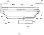
- FIG 1 is a schematic block diagram of an electromagnetic film outlet structure according to an embodiment of the present disclosure.
- an embodiment of the present disclosure includes an electromagnetic film outlet structure, which includes a backplate structure 100, an electromagnetic touch structure, and an outer frame structure 600, where the backplate structure 100 may provide support for the electromagnetic touch structure and the outer frame structure 600.
- the electromagnetic touch structure is used to provide an electromagnetic touch function, and the outer frame structure 600 may seal and support the electromagnetic touch structure and the backplate structure 100 from a peripheral side.
- the above-mentioned electromagnetic touch structure includes a diffusion plate 200 provided above the backplate structure 100, an electromagnetic film 300 provided corresponding to the diffusion plate 200, an electromagnetic touch control panel 800 provided outside the backplate structure 100, and a flexible electromagnetic circuit 700 connecting the electromagnetic film 300 and the electromagnetic touch control panel 800.
- the outer frame structure 600 is sheathed on the outside of the backplate structure 100 and surrounds the backplate structure 100 to form a sealing frame structure.
- the diffusion plate 200, the electromagnetic film 300 and the flexible electromagnetic circuit 700 are all located within the sealing frame structure, and the electromagnetic touch control panel 800 is located outside the sealing frame structure.
- the sealing frame structure formed by the backplate structure 100 and the outer frame structure 600 encloses the diffusion plate 200 and the electromagnetic film 300 therein, and by providing the flexible electromagnetic circuit 700 in the sealing frame structure, the electromagnetic film 300 located inside the sealing frame structure may be connected to the electromagnetic touch control panel 800 located outside the sealing frame structure.
- the flexible electromagnetic circuit 700 may be bendingly arranged according to the structural characteristics of the sealing frame structure, the diffusion plate 200 and the electromagnetic film 300, and may also be arranged to fit the sealing frame structure, the diffusion plate 200 and the electromagnetic film 300, to make a simple outlet of the electromagnetic film in the sealing frame structure, thereby not only implementing its electromagnetic touch function, but not destroying the integrity of the sealing frame structure, and more importantly, not affecting the optical characteristics and display effect of the entire structure.
- the flexible electromagnetic circuit 700 includes a flexible outlet circuit board 710 connected to an end of the electromagnetic film 300, and bendingly extended toward the backplate structure 100, and an adapter circuit board 720 connecting the flexible outlet circuit board 710 with the electromagnetic touch control panel 800.
- the flexible outlet circuit board 710 is located inside the outer frame structure 600, and the adapter circuit board 720 is provided inside the backplate structure 100.
- the outlet circuit of the electromagnetic film 300 namely the flexible outlet circuit board 710
- the outlet circuit of the electromagnetic film 300 may be conveniently bindingly extended from the end of the electromagnetic film 300 to the inner side of the backplate structure 100, using the flexible and bendable characteristics of the flexible outlet circuit board 710, so that the outlet of the electromagnetic film 300 inside the outer frame structure 600 and the backplate structure 100 may be easy and simple, and there is no need to destroy the integrity of the electromagnetic touch structure and the sealing frame structure.
- the flexible electromagnetic circuit 700 as the structure form of the flexible outlet circuit board 710 and the adapter circuit board 720, not only the flexible characteristics of the flexible outlet circuit board 710 may be used to the outlet of the electromagnetic film 300, but also the adapter circuit board 720 may be configured as an ordinary circuit board, thereby reducing the cost of the flexible electromagnetic circuit 700.
- the above-mentioned flexible electromagnetic circuit may include a plurality of flexible outlet circuit boards 710 connected to one or both ends of the electromagnetic film 300, and at least one adapter circuit board 720 connected to the plurality of flexible outlet circuit boards 710.
- one or more electromagnetic films 300 may be provided on the diffusion plate 200, and these electromagnetic films 300 may be located at different positions of the diffusion plate 200. That is, the plurality of flexible outlet circuit boards 710 may be used for the connection through the outlet to one or more electromagnetic films 300, and these flexible outlet circuit boards 710 may be provided on one or both ends or multiple ends of the electromagnetic films 300, to make it possible to achieve multiple outlets for one electromagnetic film 300, or to achieve outlets for multiple electromagnetic films 300, respectively.
- the flexible outlet circuit boards 710 may be wired and switched through one or more adapter circuit boards 720, so that the flexible outlet circuit boards 710 located at different positions may be switched freely and conveniently.
- the adapter circuit board 720 may be pre-fixed inside the backplate structure 100, so that only the flexible outlet circuit board 710 needs to be connected to the adapter circuit board 720 during the assembly process, which is simple and convenient.
- the flexible outlet circuit board 710 may also be set as a circuit structure with connection-pegs at both ends, and may be easily inserted on the electromagnetic film 300 and the adapter circuit board 720 through the connection-pegs.
- the flexible electromagnetic circuit 700 further includes a cable 730 connected to the adapter circuit board 720, and the cable 730 may pass through the backplate structure 100 and be connect to the electromagnetic touch control panel 800.
- the connection between the electromagnetic film 300 and the electromagnetic touch control panel 800 is achieved through the flexible outlet circuit board 710, the adapter circuit board 720, and the cable 730, so as to realize the electromagnetic touch function.
- the cable 730 may directly pass through the backplate structure 100, that is, a hole is trepanned on the backplate structure 100 to realize the cable threading; and the cable 730 may also bypass the backplate structure 100 and pass through a gap of the backplate structure 100.
- the back plate structure 100 includes a backplate mainboard 110, and inclined plates 120 respectively provided obliquely on both sides of the backplate mainboard 110.
- the outer frame structure 600 is sheathed outside the inclined plates 120 on both sides, thereby forming the above-mentioned sealing frame structure.
- the flexible outlet circuit board 710 is bendingly extended from the end of the electromagnetic film 300 via the inner side of the outer frame structure 600 (mainly refers to the side facing the end of the electromagnetic film 300) to the inner side of the inclined plate 120 (mainly refers to the side facing the diffusion plate 200), and the adapter circuit board 720 is located inside the inclined plate 120, and the cable 730 may pass through the backplate mainboard 110 to connect to the electromagnetic touch control panel 800.
- the adapter circuit board 720 may be pre-fixed on the inner side of the inclined plate 120 of the back plate structure 100.
- the above-mentioned electromagnetic film outlet structure further includes a reflector 500 provided on the inner side of the backplate structure 100 (mainly refers to the side facing the diffusion plate 200) and corresponding to the diffusion plate 200.
- the flexible outlet circuit board 710, the adapter circuit board 720 and the cable 730 are all provided between the reflector 500 and the backplate structure 100. That is, the flexible electromagnetic circuit 700 is sandwiched between the reflector 500 and the backplate structure 100, which is convenient for tracing and does not affect the arrangement of the optical structure and the entire structure and does not affect the optical characteristics and display effect of the structure.
- the shape of the reflector 500 and the shape of the back plate structure 100 correspond to each other.
- the reflector 500 includes a main reflector plate corresponding to the backplate mainboard 110, and side reflector plates respectively provided obliquely on both sides of the main reflector.
- the side reflector plates correspond to the inclined plate 120 one-to-one, and the flexible outlet circuit board 710 is bendingly extended to the area between the side reflector side plates and the inclined plate 120.
- the adapter circuit board 720 is located between the inclined plate 120 and the side reflector plate, the cable 730 is located between the main reflector plate and the backplate mainboard. In this way, the structure of the reflector 500 may be kept corresponding to the structure of the backplate structure 100, thereby facilitating the positioning and wiring of the flexible electromagnetic circuit 700.
- the electromagnetic film 300 may be provided on the top of the diffusion plate 200 (refers to the side of the diffusion plate 200 facing away from the back plate structure 100), and the above-mentioned electromagnetic touch structure further includes an optical film 400 provided on the electromagnetic film 300.
- the electromagnetic film 300 may also be provided at the bottom of the diffusion plate 200 (refers to the side of the diffusion plate 200 facing the backplate structure 100), and the above-mentioned electromagnetic touch structure further includes an optical film 400 provided on the diffusion plate 200. That is, the electromagnetic film 300 may be provided above or below the diffusion plate 200.
- the above-mentioned electromagnetic touch structure may further include an optical film 400 provided on the electromagnetic film 300 or on the diffusion plate 200, and the optical film 400 is also located in the outer frame structure 600.
- the electromagnetic film 300 may be provided on the top or bottom of the diffusion plate 200 in a full fitting or frame fitting manner.
- the present disclosure further provides a direct-type backlight display module which includes the electromagnetic film outlet structure as described above.
- the present disclosure further provides a display which includes the direct-type backlight display module as described above.
- the flexible electromagnetic circuit may trace along the inner of the sealing frame structure, the diffusion plate and the reflector, which will not affect the integrity of the entire structure, nor will it affect the optical performance and the display effect of the direct-type backlight display module and the display.
Landscapes
- Engineering & Computer Science (AREA)
- Physics & Mathematics (AREA)
- General Engineering & Computer Science (AREA)
- Theoretical Computer Science (AREA)
- General Physics & Mathematics (AREA)
- Human Computer Interaction (AREA)
- Nonlinear Science (AREA)
- Electromagnetism (AREA)
- Chemical & Material Sciences (AREA)
- Crystallography & Structural Chemistry (AREA)
- Mathematical Physics (AREA)
- Optics & Photonics (AREA)
- Devices For Indicating Variable Information By Combining Individual Elements (AREA)
- Liquid Crystal (AREA)
- Planar Illumination Modules (AREA)
Abstract
Description
- The present disclosure relates to the field of LED display device technologies and, in particular, to an electromagnetic film outlet structure, a type of direct-type backlight display module and display.
- In conventional technologies, a direct backlight display can only be used as a display as a single function. With the development of input technology and display technology, it is a market development trend to combine a commonly used liquid crystal display and a commonly used touch apparatus. Moreover, the market demands increasingly better user experience of touch input, such as the pursuit of handwriting input effect of original handwriting. Thus electromagnetic touch screen technology has been widely deployed, and the electromagnetic touch screen technology has also begun to be deployed in the direct-type backlight display. Moreover, in a backlight display module, an electromagnetic film needs to be connected to an electromagnetic touch control panel through a cable. However, the electromagnetic film needs to be installed inside the backlight display module, and the electromagnetic touch control panel needs to be installed outside the backlight display module. Because the backlight display module in conventional technologies is generally configured as an integrated body, it is very difficult to outlet the electromagnetic film located inside the backlight display module, and it cannot connect the electromagnetic film with the electromagnetic touch control panel without destroying the integrity of the backlight display module and without affecting the display effect of the backlight display module.
- To solve the above-identified and other technical problems, the present disclosure provides an electromagnetic film outlet structure, a direct-type backlight display module and a display, which may facilitate the outlet of an electromagnetic film, and easily implement the connection between the electromagnetic film and electromagnetic touch control panel.
- The technical solution is as follows:
- an electromagnetic film outlet structure, including a backplate structure, an electromagnetic touch structure, and an outer frame structure;
- the electromagnetic touch structure includes a diffusion plate provided above the backplate structure, an electromagnetic film provided corresponding to the diffusion plate, an electromagnetic touch control panel provided outside the backplate structure, and a flexible electromagnetic circuit connecting the electromagnetic film and the electromagnetic touch control panel; and
- the outer frame structure is sheathed on outside the backplate structure to form a sealing frame structure with the backplate structure, and the diffusion plate, the electromagnetic film and the flexible electromagnetic circuit are all located in the sealing frame structure, and the electromagnetic touch control panel is located outside the sealing frame structure.
- The structures, such as diffusion plate and the electromagnetic film, are enclosed inside the sealing frame structure formed by the backplate structure and the outer frame structure, and the flexible electromagnetic circuit installed in the sealing frame structure connects the electromagnetic film located inside the sealing frame structure with the electromagnetic touch control panel located outside the sealing frame structure. Since the flexible electromagnetic circuit has characteristics of being bendable and foldable as a flexible circuit, the flexible electromagnetic circuit may be bendingly arranged according to the structural characteristics of the sealing frame structure, the diffusion plate and the electromagnetic film, or the flexible electromagnetic circuit may be arranged to fit the sealing frame structure, the diffusion plate and the electromagnetic film, so that it is easy to provide the outlet of the electromagnetic film located inside the sealing frame structure, thereby not only implementing its electromagnetic touch function, but also not destroying the integrity of the sealing frame structure, and more importantly, not affecting optical characteristics and display effect of the entire structure.
- The technical solutions are further described below:
- further, the flexible electromagnetic circuit includes a flexible outlet circuit board connected to an end of the electromagnetic film and bendingly extended toward the backplate structure, and an adapter circuit board connecting the flexible outlet circuit board with the electromagnetic touch control panel, where the flexible outlet circuit board is located inside the outer frame structure, and the adapter circuit board is provided inside the backplate structure.
- Further, the flexible electromagnetic circuit includes a number of the flexible outlet circuit boards connected to one or both ends of the electromagnetic film, and at least one of the adapter circuit boards is connected to the flexible outlet circuit boards.
- Further, the flexible electromagnetic circuit includes a cable connected to the adapter circuit board, where the cable passes through the backplate structure to connect to the electromagnetic touch control panel.
- Further, the backplate structure includes a backplate mainboard, and inclined plates respectively provided obliquely on both sides of the backplate mainboard, and the outer frame structure is sheathed outside the inclined plates on both sides;
- and the flexible outlet circuit board is bendingly extended from the end of the electromagnetic film via the inner side of the outer frame structure to the inner side of the inclined plate, the adapter circuit board is located on the inner side of the inclined plate, and the cable passes through the backplate mainboard and is connected to the electromagnetic touch control panel.
- Further, it also includes a reflector provided on the inner side of the backplate structure and corresponding to the diffusion plate, where the flexible outlet circuit board, the adapter circuit board and the cable are all provided between the reflector and the backplate structure.
- Further, a shape of the reflector corresponds to a shape of the backplate structure, the reflector includes a main reflector plate corresponding to the backplate mainboard and side reflector plates respectively inclined on both sides of the main reflector plate, where the side reflector plates correspond to the inclined plate one-to-one, and the flexible outlet circuit board is bindingly extended to the area between the side reflector plates and the inclined plate, the adapter circuit board is located between the inclined plate and the side reflector plates, and the cable is located between the main reflector and the backplate mainboard.
- Further, the electromagnetic film is provided on top of the diffusion plate, and the electromagnetic touch structure further includes an optical film provided on the electromagnetic film; or
- the electromagnetic film is provided at bottom of the diffusion plate, and the electromagnetic touch structure further includes an optical film provided on the diffusion plate.
- In addition, the present disclosure further provides a direct-type backlight display module including the above-mentioned electromagnetic film outlet structure as described above.
- In addition, the present disclosure further provides a display including the direct-type backlight display module as described above.
- The present disclosure has the following beneficial effects: by providing a flexible electromagnetic circuit with characteristics of being bendable and deformable, it easily achieves the outlet of the electromagnetic film in the sealing frame structure, the flexible electromagnetic circuit may trace along the inner of the sealing frame structure, the diffusion plate and the reflector, which will not affect the integrity of the entire structure, nor will it affect optical characteristics and display effect of the direct-type backlight display module and the display.
-
FIG 1 is a schematic block diagram of an electromagnetic film outlet structure according to an embodiment of the present disclosure. - Illustration of reference signs:
- 100-Backplate structure, 110-Backplate mainboard, 120-Inclined plate, 200-Diffusion plate, 300-Electromagnetic film, 400-Optical film, 500-Reflector, 600-Outer frame structure, 700-Flexible electromagnetic circuit, 710-Flexible outlet circuit board, 720-Adapter circuit board, 730-Cable, 800-Electromagnetic touch control panel.
- Embodiments of the present disclosure are described in detail below, and examples of the embodiments are shown in the drawing. The embodiments described below with reference to the drawing are exemplary, and are only used to explain the present disclosure, and are not understood as limitations to the present disclosure.
- As shown in
FIG. 1 , an embodiment of the present disclosure includes an electromagnetic film outlet structure, which includes abackplate structure 100, an electromagnetic touch structure, and anouter frame structure 600, where thebackplate structure 100 may provide support for the electromagnetic touch structure and theouter frame structure 600. The electromagnetic touch structure is used to provide an electromagnetic touch function, and theouter frame structure 600 may seal and support the electromagnetic touch structure and thebackplate structure 100 from a peripheral side. - Specifically, the above-mentioned electromagnetic touch structure includes a
diffusion plate 200 provided above thebackplate structure 100, anelectromagnetic film 300 provided corresponding to thediffusion plate 200, an electromagnetictouch control panel 800 provided outside thebackplate structure 100, and a flexibleelectromagnetic circuit 700 connecting theelectromagnetic film 300 and the electromagnetictouch control panel 800. Moreover, theouter frame structure 600 is sheathed on the outside of thebackplate structure 100 and surrounds thebackplate structure 100 to form a sealing frame structure. Thediffusion plate 200, theelectromagnetic film 300 and the flexibleelectromagnetic circuit 700 are all located within the sealing frame structure, and the electromagnetictouch control panel 800 is located outside the sealing frame structure. In this way, the sealing frame structure formed by thebackplate structure 100 and theouter frame structure 600 encloses thediffusion plate 200 and theelectromagnetic film 300 therein, and by providing the flexibleelectromagnetic circuit 700 in the sealing frame structure, theelectromagnetic film 300 located inside the sealing frame structure may be connected to the electromagnetictouch control panel 800 located outside the sealing frame structure. Since the flexibleelectromagnetic circuit 700 has the characteristics of being bendable and foldable as a flexible circuit, the flexibleelectromagnetic circuit 700 may be bendingly arranged according to the structural characteristics of the sealing frame structure, thediffusion plate 200 and theelectromagnetic film 300, and may also be arranged to fit the sealing frame structure, thediffusion plate 200 and theelectromagnetic film 300, to make a simple outlet of the electromagnetic film in the sealing frame structure, thereby not only implementing its electromagnetic touch function, but not destroying the integrity of the sealing frame structure, and more importantly, not affecting the optical characteristics and display effect of the entire structure. - Moreover, the flexible
electromagnetic circuit 700 includes a flexibleoutlet circuit board 710 connected to an end of theelectromagnetic film 300, and bendingly extended toward thebackplate structure 100, and anadapter circuit board 720 connecting the flexibleoutlet circuit board 710 with the electromagnetictouch control panel 800. The flexibleoutlet circuit board 710 is located inside theouter frame structure 600, and theadapter circuit board 720 is provided inside thebackplate structure 100. By providing the flexibleoutlet circuit board 710 at the end of theelectromagnetic film 300, and providing theadapter circuit board 720 on the inner side of thebackplate structure 100, the outlet circuit of theelectromagnetic film 300, namely the flexibleoutlet circuit board 710, may be conveniently bindingly extended from the end of theelectromagnetic film 300 to the inner side of thebackplate structure 100, using the flexible and bendable characteristics of the flexibleoutlet circuit board 710, so that the outlet of theelectromagnetic film 300 inside theouter frame structure 600 and thebackplate structure 100 may be easy and simple, and there is no need to destroy the integrity of the electromagnetic touch structure and the sealing frame structure. In addition, by providing the flexibleelectromagnetic circuit 700 as the structure form of the flexibleoutlet circuit board 710 and theadapter circuit board 720, not only the flexible characteristics of the flexibleoutlet circuit board 710 may be used to the outlet of theelectromagnetic film 300, but also theadapter circuit board 720 may be configured as an ordinary circuit board, thereby reducing the cost of the flexibleelectromagnetic circuit 700. - Further, the above-mentioned flexible electromagnetic circuit may include a plurality of flexible
outlet circuit boards 710 connected to one or both ends of theelectromagnetic film 300, and at least oneadapter circuit board 720 connected to the plurality of flexibleoutlet circuit boards 710. Moreover, one or moreelectromagnetic films 300 may be provided on thediffusion plate 200, and theseelectromagnetic films 300 may be located at different positions of thediffusion plate 200. That is, the plurality of flexibleoutlet circuit boards 710 may be used for the connection through the outlet to one or moreelectromagnetic films 300, and these flexibleoutlet circuit boards 710 may be provided on one or both ends or multiple ends of theelectromagnetic films 300, to make it possible to achieve multiple outlets for oneelectromagnetic film 300, or to achieve outlets for multipleelectromagnetic films 300, respectively. Moreover, the flexibleoutlet circuit boards 710 may be wired and switched through one or moreadapter circuit boards 720, so that the flexibleoutlet circuit boards 710 located at different positions may be switched freely and conveniently. In addition, theadapter circuit board 720 may be pre-fixed inside thebackplate structure 100, so that only the flexibleoutlet circuit board 710 needs to be connected to theadapter circuit board 720 during the assembly process, which is simple and convenient. In addition, the flexibleoutlet circuit board 710 may also be set as a circuit structure with connection-pegs at both ends, and may be easily inserted on theelectromagnetic film 300 and theadapter circuit board 720 through the connection-pegs. - In addition, the flexible
electromagnetic circuit 700 further includes acable 730 connected to theadapter circuit board 720, and thecable 730 may pass through thebackplate structure 100 and be connect to the electromagnetictouch control panel 800. Thus, the connection between theelectromagnetic film 300 and the electromagnetictouch control panel 800 is achieved through the flexibleoutlet circuit board 710, theadapter circuit board 720, and thecable 730, so as to realize the electromagnetic touch function. Moreover, thecable 730 may directly pass through thebackplate structure 100, that is, a hole is trepanned on thebackplate structure 100 to realize the cable threading; and thecable 730 may also bypass thebackplate structure 100 and pass through a gap of thebackplate structure 100. In this way, it is convenient to fix theadapter circuit board 720 on thebackplate structure 100 in advance, and then conveniently connects theadapter circuit board 720 connected to the flexibleoutlet circuit board 710 to the electromagnetictouch control panel 800 by setting thecable 730, thereby facilitating the outlet of theelectromagnetic film 300. - In addition, the
back plate structure 100 includes abackplate mainboard 110, andinclined plates 120 respectively provided obliquely on both sides of thebackplate mainboard 110. Theouter frame structure 600 is sheathed outside theinclined plates 120 on both sides, thereby forming the above-mentioned sealing frame structure. Moreover, the flexibleoutlet circuit board 710 is bendingly extended from the end of theelectromagnetic film 300 via the inner side of the outer frame structure 600 (mainly refers to the side facing the end of the electromagnetic film 300) to the inner side of the inclined plate 120 (mainly refers to the side facing the diffusion plate 200), and theadapter circuit board 720 is located inside theinclined plate 120, and thecable 730 may pass through thebackplate mainboard 110 to connect to the electromagnetictouch control panel 800. That is, according to the structural characteristics of thebackplate structure 100, theelectromagnetic film 300, thediffusion plate 200 and theouter frame structure 600, the flexibleoutlet circuit board 710 and theadapter circuit board 720 are provided along the inner side of these structures, which will not affect the structural arrangement of the entire structure, i.e. will not affect the sealing, connection and supporting performance of its original structure, nor will it affect the optical characteristics and display effect of its original structure. In the embodiment, theadapter circuit board 720 may be pre-fixed on the inner side of theinclined plate 120 of theback plate structure 100. - In addition, the above-mentioned electromagnetic film outlet structure further includes a
reflector 500 provided on the inner side of the backplate structure 100 (mainly refers to the side facing the diffusion plate 200) and corresponding to thediffusion plate 200. The flexibleoutlet circuit board 710, theadapter circuit board 720 and thecable 730 are all provided between thereflector 500 and thebackplate structure 100. That is, the flexibleelectromagnetic circuit 700 is sandwiched between thereflector 500 and thebackplate structure 100, which is convenient for tracing and does not affect the arrangement of the optical structure and the entire structure and does not affect the optical characteristics and display effect of the structure. Further, the shape of thereflector 500 and the shape of theback plate structure 100 correspond to each other. Specifically, thereflector 500 includes a main reflector plate corresponding to thebackplate mainboard 110, and side reflector plates respectively provided obliquely on both sides of the main reflector. The side reflector plates correspond to theinclined plate 120 one-to-one, and the flexibleoutlet circuit board 710 is bendingly extended to the area between the side reflector side plates and theinclined plate 120. Theadapter circuit board 720 is located between theinclined plate 120 and the side reflector plate, thecable 730 is located between the main reflector plate and the backplate mainboard. In this way, the structure of thereflector 500 may be kept corresponding to the structure of thebackplate structure 100, thereby facilitating the positioning and wiring of the flexibleelectromagnetic circuit 700. - In addition, the
electromagnetic film 300 may be provided on the top of the diffusion plate 200 (refers to the side of thediffusion plate 200 facing away from the back plate structure 100), and the above-mentioned electromagnetic touch structure further includes anoptical film 400 provided on theelectromagnetic film 300. Or, theelectromagnetic film 300 may also be provided at the bottom of the diffusion plate 200 (refers to the side of thediffusion plate 200 facing the backplate structure 100), and the above-mentioned electromagnetic touch structure further includes anoptical film 400 provided on thediffusion plate 200. That is, theelectromagnetic film 300 may be provided above or below thediffusion plate 200. The above-mentioned electromagnetic touch structure may further include anoptical film 400 provided on theelectromagnetic film 300 or on thediffusion plate 200, and theoptical film 400 is also located in theouter frame structure 600. Moreover, theelectromagnetic film 300 may be provided on the top or bottom of thediffusion plate 200 in a full fitting or frame fitting manner. By providing theoptical film 400, the optical characteristics and display effect may be realized and enhanced, and theelectromagnetic film 300 may also be protected. - In addition, the present disclosure further provides a direct-type backlight display module which includes the electromagnetic film outlet structure as described above. In addition, the present disclosure further provides a display which includes the direct-type backlight display module as described above. In the direct-type backlight display module and the display, by providing flexible electromagnetic circuit with characteristics of being bendable and deformable, it easily achieves the outlet of the electromagnetic film in the sealing frame structure, the flexible electromagnetic circuit may trace along the inner of the sealing frame structure, the diffusion plate and the reflector, which will not affect the integrity of the entire structure, nor will it affect the optical performance and the display effect of the direct-type backlight display module and the display.
- In addition, it should also be understood that, in the embodiment, the positional relationships indicated by the terms, such as "down", "up", "front", "rear", "left", "right", "inner", "outer", "top", "bottom", "one side", "the other side", "one end", "the other end", are based on the positional relationship shown in the drawing; and the terms, such as "first", "second", are used to distinguish different structural components. These terms are only used to facilitate describing the present disclosure and simplifying the description, and should not be understood as limiting the present disclosure.
- The technical features of the above-mentioned embodiments may be combined arbitrarily, in order to make the description concise, all possible combinations of the technical features in the embodiments are not all described, however, as long as there is no contradiction among the combinations of these technical features, it should be regarded as the scope of the description.
- The above-mentioned embodiments only express several implementations of the present disclosure with a specific and detailed description, but they cannot therefore be understood as limitations on the scope of the present disclosure. It should be pointed out that for those of ordinary skilled in the art, without departing from the concept of the present disclosure, several modifications and improvements can be made, all of which fall within the protection scope of the present disclosure. Therefore, the protection scope of the present disclosure should be subject to the attached claims.
Claims (10)
- An electromagnetic film outlet structure, comprising a backplate structure, an electromagnetic touch structure, and an outer frame structure,
wherein the electromagnetic touch structure comprises a diffusion plate provided above the backplate structure, an electromagnetic film provided corresponding to the diffusion plate, an electromagnetic touch control panel provided outside the backplate structure, and a flexible electromagnetic circuit connecting the electromagnetic film and the electromagnetic touch control panel, and
the outer frame structure is sheathed outside the backplate structure and a sealing frame structure is formed by the outer frame structure and the backplate structure, and the diffusion plate, the electromagnetic film and the flexible electromagnetic circuit are all located in the sealing frame structure, and the electromagnetic touch control panel is located outside the sealing frame structure. - The electromagnetic film outlet structure according to claim 1, wherein the flexible electromagnetic circuit comprises a flexible outlet circuit board connected to an end of the electromagnetic film and bendingly extended toward the backplate structure, and an adapter circuit board connecting the flexible outlet circuit board with the electromagnetic touch control panel, wherein the flexible outlet circuit board is located inside the outer frame structure, and the adapter circuit board is provided inside the backplate structure.
- The electromagnetic film outlet structure according to claim 2, wherein the flexible electromagnetic circuit comprises a plurality of the flexible outlet circuit boards connected to one or both ends of the electromagnetic film, and at least one adapter circuit board connected to the plurality of flexible outlet circuit boards.
- The electromagnetic film outlet structure according to claim 2 or 3, wherein the flexible electromagnetic circuit further comprises a cable connected to the adapter circuit board, wherein the cable passes through the backplate structure to connect to the electromagnetic touch control panel.
- The electromagnetic film outlet structure according to claim 4, wherein the backplate structure comprises a backplate mainboard and inclined plates respectively provided obliquely on both sides of the backplate mainboard, and the outer frame structure is sheathed outside the inclined plates on both sides; and the flexible outlet circuit board is bendingly extended from the end of the electromagnetic film via the inner side of the outer frame structure to the inner side of the inclined plate, and the adapter circuit board is located on the inner side of the inclined plate, and the cable passes through the backplate mainboard and is connected to the electromagnetic touch control panel.
- The electromagnetic film outlet structure according to claim 5, further comprising a reflector provided on the inner side of the backplate structure and corresponding to the diffusion plate, wherein the flexible outlet circuit board, the adapter circuit board and the cable are all provided between the reflector and the backplate structure.
- The electromagnetic film outlet structure according to claim 6, wherein a shape of the reflector corresponds to a shape of the backplate structure, the reflector comprises a main reflector plate corresponding to the backplate mainboard and side reflectors plates respectively inclined on both sides of the main reflector plate, wherein the side reflectors plates correspond to the inclined plate one-to-one, and the flexible outlet circuit board is bendingly extended to the area between the side reflector plate and the inclined plate, the adapter circuit board is located between the inclined plate and the side reflector plate, and the cable is located between the main reflector plate and the backplate mainboard.
- The electromagnetic film outlet structure according to claim 2 or 3, wherein the electromagnetic film is provided on top of the diffusion plate, and the electromagnetic touch structure further comprises an optical film provided on the electromagnetic film; or
the electromagnetic film is provided at bottom of the diffusion plate, and the electromagnetic touch structure further comprises an optical film provided on the diffusion plate. - A direct-type backlight display module, comprising the electromagnetic film outlet structure according to any one of claims 1-8.
- A display, comprising the direct-type backlight display module according to claim 9.
Applications Claiming Priority (2)
| Application Number | Priority Date | Filing Date | Title |
|---|---|---|---|
| CN201820658093.0U CN208367669U (en) | 2018-05-03 | 2018-05-03 | Electromagnetic film outlet structure, direct type backlight display module and display |
| PCT/CN2018/118463 WO2019210682A1 (en) | 2018-05-03 | 2018-11-30 | Electromagnetic film wire-out structure, direct-type backlight display module and display |
Publications (3)
| Publication Number | Publication Date |
|---|---|
| EP3789863A1 true EP3789863A1 (en) | 2021-03-10 |
| EP3789863A4 EP3789863A4 (en) | 2021-06-23 |
| EP3789863B1 EP3789863B1 (en) | 2025-01-15 |
Family
ID=64933732
Family Applications (1)
| Application Number | Title | Priority Date | Filing Date |
|---|---|---|---|
| EP18917349.5A Active EP3789863B1 (en) | 2018-05-03 | 2018-11-30 | Electromagnetic film wire-out structure, direct-type backlight display module and display |
Country Status (5)
| Country | Link |
|---|---|
| US (1) | US11281348B2 (en) |
| EP (1) | EP3789863B1 (en) |
| JP (1) | JP7004848B2 (en) |
| CN (1) | CN208367669U (en) |
| WO (1) | WO2019210682A1 (en) |
Family Cites Families (9)
| Publication number | Priority date | Publication date | Assignee | Title |
|---|---|---|---|---|
| JPH0713144A (en) * | 1993-06-24 | 1995-01-17 | Canon Inc | Liquid crystal display |
| US7030860B1 (en) * | 1999-10-08 | 2006-04-18 | Synaptics Incorporated | Flexible transparent touch sensing system for electronic devices |
| US7154570B2 (en) * | 2002-09-28 | 2006-12-26 | Samsung Electronics Co., Ltd. | Back light assembly, liquid crystal display apparatus and manufacturing method thereof |
| US7755616B2 (en) | 2003-03-28 | 2010-07-13 | Lg Display Co., Ltd. | Liquid crystal display device having electromagnetic type touch panel |
| TW201250347A (en) * | 2011-06-07 | 2012-12-16 | Au Optronics Corp | Touch LCD apparatus |
| CN104679339B (en) * | 2015-01-19 | 2016-08-17 | 欧浦登(顺昌)光学有限公司 | A kind of hermetically sealed liquid crystal integrated screen and manufacturing process thereof |
| KR102556829B1 (en) * | 2016-06-29 | 2023-07-19 | 삼성디스플레이 주식회사 | Display panel having touch functuion and display apparatus including thereof |
| KR102668848B1 (en) * | 2016-08-04 | 2024-05-24 | 삼성디스플레이 주식회사 | Liquid crystal display device |
| CN106980207B (en) * | 2017-05-12 | 2023-09-01 | 广州视源电子科技股份有限公司 | Direct-lit backlight display module and display device |
-
2018
- 2018-05-03 CN CN201820658093.0U patent/CN208367669U/en active Active
- 2018-11-30 JP JP2020561721A patent/JP7004848B2/en active Active
- 2018-11-30 EP EP18917349.5A patent/EP3789863B1/en active Active
- 2018-11-30 WO PCT/CN2018/118463 patent/WO2019210682A1/en not_active Ceased
-
2020
- 2020-10-30 US US17/085,580 patent/US11281348B2/en active Active
Also Published As
| Publication number | Publication date |
|---|---|
| EP3789863A4 (en) | 2021-06-23 |
| US11281348B2 (en) | 2022-03-22 |
| EP3789863B1 (en) | 2025-01-15 |
| CN208367669U (en) | 2019-01-11 |
| JP2021520576A (en) | 2021-08-19 |
| JP7004848B2 (en) | 2022-01-21 |
| WO2019210682A1 (en) | 2019-11-07 |
| US20210048903A1 (en) | 2021-02-18 |
Similar Documents
| Publication | Publication Date | Title |
|---|---|---|
| JP5032651B2 (en) | Television receiver and electronic device | |
| WO2019006794A1 (en) | Liquid crystal display panel and liquid crystal display module | |
| CN108897174A (en) | screen assembly and electronic device | |
| KR20160082556A (en) | Display Device | |
| CN102338944A (en) | Liquid crystal display device | |
| US20200089041A1 (en) | Full display screen and display device with the full display screen | |
| JP2009080947A (en) | Surface light source device and liquid crystal display device using the same | |
| JP7271162B2 (en) | Electronics | |
| WO2017190379A1 (en) | Liquid crystal display apparatus | |
| JP2018142014A (en) | Display device | |
| US20150268506A1 (en) | Curved liquid crystal display device | |
| CN204806078U (en) | Backlight module and touch display device | |
| WO2016183902A1 (en) | Backlight module and liquid crystal display device | |
| CN112083600A (en) | Liquid crystal display screen and mobile terminal | |
| US11442307B2 (en) | Backlight module, display module and assembling method thereof | |
| KR20130074794A (en) | Display device | |
| WO2016104360A1 (en) | Illumination device and display device | |
| CN108319063A (en) | Electronic device, display assembly and backlight module thereof | |
| US9500892B2 (en) | Liquid crystal module and display device | |
| US11281348B2 (en) | Electromagnetic film outlet structure, direct-type backlight display module and display | |
| CN205318064U (en) | Backlight module and display device | |
| CN108205222A (en) | Back light unit and the liquid crystal display device including the back light unit | |
| JP5271653B2 (en) | Liquid crystal device and electronic device | |
| TWI381214B (en) | Backlight module and display apparatus | |
| CN108828855A (en) | Display device |
Legal Events
| Date | Code | Title | Description |
|---|---|---|---|
| STAA | Information on the status of an ep patent application or granted ep patent |
Free format text: STATUS: THE INTERNATIONAL PUBLICATION HAS BEEN MADE |
|
| PUAI | Public reference made under article 153(3) epc to a published international application that has entered the european phase |
Free format text: ORIGINAL CODE: 0009012 |
|
| STAA | Information on the status of an ep patent application or granted ep patent |
Free format text: STATUS: REQUEST FOR EXAMINATION WAS MADE |
|
| 17P | Request for examination filed |
Effective date: 20201203 |
|
| AK | Designated contracting states |
Kind code of ref document: A1 Designated state(s): AL AT BE BG CH CY CZ DE DK EE ES FI FR GB GR HR HU IE IS IT LI LT LU LV MC MK MT NL NO PL PT RO RS SE SI SK SM TR |
|
| AX | Request for extension of the european patent |
Extension state: BA ME |
|
| A4 | Supplementary search report drawn up and despatched |
Effective date: 20210521 |
|
| RIC1 | Information provided on ipc code assigned before grant |
Ipc: G06F 3/046 20060101AFI20210517BHEP Ipc: G06F 3/044 20060101ALI20210517BHEP Ipc: G06F 3/045 20060101ALI20210517BHEP Ipc: G06F 3/047 20060101ALI20210517BHEP Ipc: G02F 1/13357 20060101ALI20210517BHEP |
|
| DAV | Request for validation of the european patent (deleted) | ||
| DAX | Request for extension of the european patent (deleted) | ||
| STAA | Information on the status of an ep patent application or granted ep patent |
Free format text: STATUS: EXAMINATION IS IN PROGRESS |
|
| 17Q | First examination report despatched |
Effective date: 20220509 |
|
| REG | Reference to a national code |
Ref country code: DE Free format text: PREVIOUS MAIN CLASS: G06F0003046000 Ref country code: DE Ref legal event code: R079 Ref document number: 602018078609 Country of ref document: DE Free format text: PREVIOUS MAIN CLASS: G06F0003046000 Ipc: G02F0001133300 |
|
| GRAP | Despatch of communication of intention to grant a patent |
Free format text: ORIGINAL CODE: EPIDOSNIGR1 |
|
| STAA | Information on the status of an ep patent application or granted ep patent |
Free format text: STATUS: GRANT OF PATENT IS INTENDED |
|
| RIC1 | Information provided on ipc code assigned before grant |
Ipc: G06F 3/047 20060101ALI20241001BHEP Ipc: G06F 3/046 20060101ALI20241001BHEP Ipc: G06F 3/045 20060101ALI20241001BHEP Ipc: G06F 3/044 20060101ALI20241001BHEP Ipc: G02F 1/13357 20060101ALI20241001BHEP Ipc: G02F 1/1333 20060101AFI20241001BHEP |
|
| INTG | Intention to grant announced |
Effective date: 20241010 |
|
| GRAS | Grant fee paid |
Free format text: ORIGINAL CODE: EPIDOSNIGR3 |
|
| GRAA | (expected) grant |
Free format text: ORIGINAL CODE: 0009210 |
|
| STAA | Information on the status of an ep patent application or granted ep patent |
Free format text: STATUS: THE PATENT HAS BEEN GRANTED |
|
| AK | Designated contracting states |
Kind code of ref document: B1 Designated state(s): AL AT BE BG CH CY CZ DE DK EE ES FI FR GB GR HR HU IE IS IT LI LT LU LV MC MK MT NL NO PL PT RO RS SE SI SK SM TR |
|
| REG | Reference to a national code |
Ref country code: CH Ref legal event code: EP Ref country code: GB Ref legal event code: FG4D |
|
| REG | Reference to a national code |
Ref country code: DE Ref legal event code: R096 Ref document number: 602018078609 Country of ref document: DE |
|
| P01 | Opt-out of the competence of the unified patent court (upc) registered |
Free format text: CASE NUMBER: APP_672/2025 Effective date: 20250108 |
|
| REG | Reference to a national code |
Ref country code: IE Ref legal event code: FG4D Ref country code: NL Ref legal event code: FP |
|
| PG25 | Lapsed in a contracting state [announced via postgrant information from national office to epo] |
Ref country code: RS Free format text: LAPSE BECAUSE OF FAILURE TO SUBMIT A TRANSLATION OF THE DESCRIPTION OR TO PAY THE FEE WITHIN THE PRESCRIBED TIME-LIMIT Effective date: 20250415 |
|
| PG25 | Lapsed in a contracting state [announced via postgrant information from national office to epo] |
Ref country code: FI Free format text: LAPSE BECAUSE OF FAILURE TO SUBMIT A TRANSLATION OF THE DESCRIPTION OR TO PAY THE FEE WITHIN THE PRESCRIBED TIME-LIMIT Effective date: 20250115 |
|
| PG25 | Lapsed in a contracting state [announced via postgrant information from national office to epo] |
Ref country code: PL Free format text: LAPSE BECAUSE OF FAILURE TO SUBMIT A TRANSLATION OF THE DESCRIPTION OR TO PAY THE FEE WITHIN THE PRESCRIBED TIME-LIMIT Effective date: 20250115 |
|
| PG25 | Lapsed in a contracting state [announced via postgrant information from national office to epo] |
Ref country code: ES Free format text: LAPSE BECAUSE OF FAILURE TO SUBMIT A TRANSLATION OF THE DESCRIPTION OR TO PAY THE FEE WITHIN THE PRESCRIBED TIME-LIMIT Effective date: 20250115 |
|
| REG | Reference to a national code |
Ref country code: LT Ref legal event code: MG9D |
|
| PG25 | Lapsed in a contracting state [announced via postgrant information from national office to epo] |
Ref country code: IS Free format text: LAPSE BECAUSE OF FAILURE TO SUBMIT A TRANSLATION OF THE DESCRIPTION OR TO PAY THE FEE WITHIN THE PRESCRIBED TIME-LIMIT Effective date: 20250515 Ref country code: NO Free format text: LAPSE BECAUSE OF FAILURE TO SUBMIT A TRANSLATION OF THE DESCRIPTION OR TO PAY THE FEE WITHIN THE PRESCRIBED TIME-LIMIT Effective date: 20250415 |
|
| REG | Reference to a national code |
Ref country code: AT Ref legal event code: MK05 Ref document number: 1760219 Country of ref document: AT Kind code of ref document: T Effective date: 20250115 |
|
| PG25 | Lapsed in a contracting state [announced via postgrant information from national office to epo] |
Ref country code: HR Free format text: LAPSE BECAUSE OF FAILURE TO SUBMIT A TRANSLATION OF THE DESCRIPTION OR TO PAY THE FEE WITHIN THE PRESCRIBED TIME-LIMIT Effective date: 20250115 |
|
| PG25 | Lapsed in a contracting state [announced via postgrant information from national office to epo] |
Ref country code: PT Free format text: LAPSE BECAUSE OF FAILURE TO SUBMIT A TRANSLATION OF THE DESCRIPTION OR TO PAY THE FEE WITHIN THE PRESCRIBED TIME-LIMIT Effective date: 20250515 Ref country code: LV Free format text: LAPSE BECAUSE OF FAILURE TO SUBMIT A TRANSLATION OF THE DESCRIPTION OR TO PAY THE FEE WITHIN THE PRESCRIBED TIME-LIMIT Effective date: 20250115 |
|
| PG25 | Lapsed in a contracting state [announced via postgrant information from national office to epo] |
Ref country code: BG Free format text: LAPSE BECAUSE OF FAILURE TO SUBMIT A TRANSLATION OF THE DESCRIPTION OR TO PAY THE FEE WITHIN THE PRESCRIBED TIME-LIMIT Effective date: 20250115 Ref country code: GR Free format text: LAPSE BECAUSE OF FAILURE TO SUBMIT A TRANSLATION OF THE DESCRIPTION OR TO PAY THE FEE WITHIN THE PRESCRIBED TIME-LIMIT Effective date: 20250416 |
|
| PG25 | Lapsed in a contracting state [announced via postgrant information from national office to epo] |
Ref country code: AT Free format text: LAPSE BECAUSE OF FAILURE TO SUBMIT A TRANSLATION OF THE DESCRIPTION OR TO PAY THE FEE WITHIN THE PRESCRIBED TIME-LIMIT Effective date: 20250115 |
|
| PG25 | Lapsed in a contracting state [announced via postgrant information from national office to epo] |
Ref country code: SE Free format text: LAPSE BECAUSE OF FAILURE TO SUBMIT A TRANSLATION OF THE DESCRIPTION OR TO PAY THE FEE WITHIN THE PRESCRIBED TIME-LIMIT Effective date: 20250115 |
|
| PG25 | Lapsed in a contracting state [announced via postgrant information from national office to epo] |
Ref country code: SM Free format text: LAPSE BECAUSE OF FAILURE TO SUBMIT A TRANSLATION OF THE DESCRIPTION OR TO PAY THE FEE WITHIN THE PRESCRIBED TIME-LIMIT Effective date: 20250115 |
|
| PG25 | Lapsed in a contracting state [announced via postgrant information from national office to epo] |
Ref country code: DK Free format text: LAPSE BECAUSE OF FAILURE TO SUBMIT A TRANSLATION OF THE DESCRIPTION OR TO PAY THE FEE WITHIN THE PRESCRIBED TIME-LIMIT Effective date: 20250115 |
|
| PG25 | Lapsed in a contracting state [announced via postgrant information from national office to epo] |
Ref country code: IT Free format text: LAPSE BECAUSE OF FAILURE TO SUBMIT A TRANSLATION OF THE DESCRIPTION OR TO PAY THE FEE WITHIN THE PRESCRIBED TIME-LIMIT Effective date: 20250115 |
|
| REG | Reference to a national code |
Ref country code: DE Ref legal event code: R097 Ref document number: 602018078609 Country of ref document: DE |
|
| PG25 | Lapsed in a contracting state [announced via postgrant information from national office to epo] |
Ref country code: CZ Free format text: LAPSE BECAUSE OF FAILURE TO SUBMIT A TRANSLATION OF THE DESCRIPTION OR TO PAY THE FEE WITHIN THE PRESCRIBED TIME-LIMIT Effective date: 20250115 Ref country code: EE Free format text: LAPSE BECAUSE OF FAILURE TO SUBMIT A TRANSLATION OF THE DESCRIPTION OR TO PAY THE FEE WITHIN THE PRESCRIBED TIME-LIMIT Effective date: 20250115 |
|
| PG25 | Lapsed in a contracting state [announced via postgrant information from national office to epo] |
Ref country code: RO Free format text: LAPSE BECAUSE OF FAILURE TO SUBMIT A TRANSLATION OF THE DESCRIPTION OR TO PAY THE FEE WITHIN THE PRESCRIBED TIME-LIMIT Effective date: 20250115 |
|
| PG25 | Lapsed in a contracting state [announced via postgrant information from national office to epo] |
Ref country code: SK Free format text: LAPSE BECAUSE OF FAILURE TO SUBMIT A TRANSLATION OF THE DESCRIPTION OR TO PAY THE FEE WITHIN THE PRESCRIBED TIME-LIMIT Effective date: 20250115 |
|
| PLBE | No opposition filed within time limit |
Free format text: ORIGINAL CODE: 0009261 |
|
| STAA | Information on the status of an ep patent application or granted ep patent |
Free format text: STATUS: NO OPPOSITION FILED WITHIN TIME LIMIT |
|
| PGFP | Annual fee paid to national office [announced via postgrant information from national office to epo] |
Ref country code: NL Payment date: 20251119 Year of fee payment: 8 |
|
| 26N | No opposition filed |
Effective date: 20251016 |
|
| PGFP | Annual fee paid to national office [announced via postgrant information from national office to epo] |
Ref country code: DE Payment date: 20251119 Year of fee payment: 8 |
|
| PGFP | Annual fee paid to national office [announced via postgrant information from national office to epo] |
Ref country code: GB Payment date: 20251121 Year of fee payment: 8 |
|
| PGFP | Annual fee paid to national office [announced via postgrant information from national office to epo] |
Ref country code: FR Payment date: 20251126 Year of fee payment: 8 |