EP3789819A1 - Display device - Google Patents
Display device Download PDFInfo
- Publication number
- EP3789819A1 EP3789819A1 EP20194125.9A EP20194125A EP3789819A1 EP 3789819 A1 EP3789819 A1 EP 3789819A1 EP 20194125 A EP20194125 A EP 20194125A EP 3789819 A1 EP3789819 A1 EP 3789819A1
- Authority
- EP
- European Patent Office
- Prior art keywords
- substrate
- conductive film
- film portion
- disposed
- display device
- Prior art date
- Legal status (The legal status is an assumption and is not a legal conclusion. Google has not performed a legal analysis and makes no representation as to the accuracy of the status listed.)
- Granted
Links
Images






Classifications
-
- G—PHYSICS
- G02—OPTICS
- G02F—OPTICAL DEVICES OR ARRANGEMENTS FOR THE CONTROL OF LIGHT BY MODIFICATION OF THE OPTICAL PROPERTIES OF THE MEDIA OF THE ELEMENTS INVOLVED THEREIN; NON-LINEAR OPTICS; FREQUENCY-CHANGING OF LIGHT; OPTICAL LOGIC ELEMENTS; OPTICAL ANALOGUE/DIGITAL CONVERTERS
- G02F1/00—Devices or arrangements for the control of the intensity, colour, phase, polarisation or direction of light arriving from an independent light source, e.g. switching, gating or modulating; Non-linear optics
- G02F1/01—Devices or arrangements for the control of the intensity, colour, phase, polarisation or direction of light arriving from an independent light source, e.g. switching, gating or modulating; Non-linear optics for the control of the intensity, phase, polarisation or colour
- G02F1/13—Devices or arrangements for the control of the intensity, colour, phase, polarisation or direction of light arriving from an independent light source, e.g. switching, gating or modulating; Non-linear optics for the control of the intensity, phase, polarisation or colour based on liquid crystals, e.g. single liquid crystal display cells
- G02F1/133—Constructional arrangements; Operation of liquid crystal cells; Circuit arrangements
- G02F1/1333—Constructional arrangements; Manufacturing methods
- G02F1/1345—Conductors connecting electrodes to cell terminals
- G02F1/13452—Conductors connecting driver circuitry and terminals of panels
-
- G—PHYSICS
- G02—OPTICS
- G02F—OPTICAL DEVICES OR ARRANGEMENTS FOR THE CONTROL OF LIGHT BY MODIFICATION OF THE OPTICAL PROPERTIES OF THE MEDIA OF THE ELEMENTS INVOLVED THEREIN; NON-LINEAR OPTICS; FREQUENCY-CHANGING OF LIGHT; OPTICAL LOGIC ELEMENTS; OPTICAL ANALOGUE/DIGITAL CONVERTERS
- G02F1/00—Devices or arrangements for the control of the intensity, colour, phase, polarisation or direction of light arriving from an independent light source, e.g. switching, gating or modulating; Non-linear optics
- G02F1/01—Devices or arrangements for the control of the intensity, colour, phase, polarisation or direction of light arriving from an independent light source, e.g. switching, gating or modulating; Non-linear optics for the control of the intensity, phase, polarisation or colour
- G02F1/13—Devices or arrangements for the control of the intensity, colour, phase, polarisation or direction of light arriving from an independent light source, e.g. switching, gating or modulating; Non-linear optics for the control of the intensity, phase, polarisation or colour based on liquid crystals, e.g. single liquid crystal display cells
- G02F1/133—Constructional arrangements; Operation of liquid crystal cells; Circuit arrangements
- G02F1/1333—Constructional arrangements; Manufacturing methods
- G02F1/1345—Conductors connecting electrodes to cell terminals
-
- H—ELECTRICITY
- H05—ELECTRIC TECHNIQUES NOT OTHERWISE PROVIDED FOR
- H05K—PRINTED CIRCUITS; CASINGS OR CONSTRUCTIONAL DETAILS OF ELECTRIC APPARATUS; MANUFACTURE OF ASSEMBLAGES OF ELECTRICAL COMPONENTS
- H05K1/00—Printed circuits
- H05K1/02—Details
- H05K1/11—Printed elements for providing electric connections to or between printed circuits
-
- G—PHYSICS
- G02—OPTICS
- G02F—OPTICAL DEVICES OR ARRANGEMENTS FOR THE CONTROL OF LIGHT BY MODIFICATION OF THE OPTICAL PROPERTIES OF THE MEDIA OF THE ELEMENTS INVOLVED THEREIN; NON-LINEAR OPTICS; FREQUENCY-CHANGING OF LIGHT; OPTICAL LOGIC ELEMENTS; OPTICAL ANALOGUE/DIGITAL CONVERTERS
- G02F1/00—Devices or arrangements for the control of the intensity, colour, phase, polarisation or direction of light arriving from an independent light source, e.g. switching, gating or modulating; Non-linear optics
- G02F1/01—Devices or arrangements for the control of the intensity, colour, phase, polarisation or direction of light arriving from an independent light source, e.g. switching, gating or modulating; Non-linear optics for the control of the intensity, phase, polarisation or colour
- G02F1/13—Devices or arrangements for the control of the intensity, colour, phase, polarisation or direction of light arriving from an independent light source, e.g. switching, gating or modulating; Non-linear optics for the control of the intensity, phase, polarisation or colour based on liquid crystals, e.g. single liquid crystal display cells
- G02F1/133—Constructional arrangements; Operation of liquid crystal cells; Circuit arrangements
- G02F1/1333—Constructional arrangements; Manufacturing methods
- G02F1/13336—Combining plural substrates to produce large-area displays, e.g. tiled displays
-
- G—PHYSICS
- G02—OPTICS
- G02F—OPTICAL DEVICES OR ARRANGEMENTS FOR THE CONTROL OF LIGHT BY MODIFICATION OF THE OPTICAL PROPERTIES OF THE MEDIA OF THE ELEMENTS INVOLVED THEREIN; NON-LINEAR OPTICS; FREQUENCY-CHANGING OF LIGHT; OPTICAL LOGIC ELEMENTS; OPTICAL ANALOGUE/DIGITAL CONVERTERS
- G02F1/00—Devices or arrangements for the control of the intensity, colour, phase, polarisation or direction of light arriving from an independent light source, e.g. switching, gating or modulating; Non-linear optics
- G02F1/01—Devices or arrangements for the control of the intensity, colour, phase, polarisation or direction of light arriving from an independent light source, e.g. switching, gating or modulating; Non-linear optics for the control of the intensity, phase, polarisation or colour
- G02F1/13—Devices or arrangements for the control of the intensity, colour, phase, polarisation or direction of light arriving from an independent light source, e.g. switching, gating or modulating; Non-linear optics for the control of the intensity, phase, polarisation or colour based on liquid crystals, e.g. single liquid crystal display cells
- G02F1/133—Constructional arrangements; Operation of liquid crystal cells; Circuit arrangements
- G02F1/1333—Constructional arrangements; Manufacturing methods
- G02F1/1345—Conductors connecting electrodes to cell terminals
- G02F1/13458—Terminal pads
-
- G—PHYSICS
- G02—OPTICS
- G02F—OPTICAL DEVICES OR ARRANGEMENTS FOR THE CONTROL OF LIGHT BY MODIFICATION OF THE OPTICAL PROPERTIES OF THE MEDIA OF THE ELEMENTS INVOLVED THEREIN; NON-LINEAR OPTICS; FREQUENCY-CHANGING OF LIGHT; OPTICAL LOGIC ELEMENTS; OPTICAL ANALOGUE/DIGITAL CONVERTERS
- G02F1/00—Devices or arrangements for the control of the intensity, colour, phase, polarisation or direction of light arriving from an independent light source, e.g. switching, gating or modulating; Non-linear optics
- G02F1/01—Devices or arrangements for the control of the intensity, colour, phase, polarisation or direction of light arriving from an independent light source, e.g. switching, gating or modulating; Non-linear optics for the control of the intensity, phase, polarisation or colour
- G02F1/13—Devices or arrangements for the control of the intensity, colour, phase, polarisation or direction of light arriving from an independent light source, e.g. switching, gating or modulating; Non-linear optics for the control of the intensity, phase, polarisation or colour based on liquid crystals, e.g. single liquid crystal display cells
- G02F1/133—Constructional arrangements; Operation of liquid crystal cells; Circuit arrangements
- G02F1/136—Liquid crystal cells structurally associated with a semi-conducting layer or substrate, e.g. cells forming part of an integrated circuit
- G02F1/1362—Active matrix addressed cells
- G02F1/136286—Wiring, e.g. gate line, drain line
-
- G—PHYSICS
- G02—OPTICS
- G02F—OPTICAL DEVICES OR ARRANGEMENTS FOR THE CONTROL OF LIGHT BY MODIFICATION OF THE OPTICAL PROPERTIES OF THE MEDIA OF THE ELEMENTS INVOLVED THEREIN; NON-LINEAR OPTICS; FREQUENCY-CHANGING OF LIGHT; OPTICAL LOGIC ELEMENTS; OPTICAL ANALOGUE/DIGITAL CONVERTERS
- G02F1/00—Devices or arrangements for the control of the intensity, colour, phase, polarisation or direction of light arriving from an independent light source, e.g. switching, gating or modulating; Non-linear optics
- G02F1/01—Devices or arrangements for the control of the intensity, colour, phase, polarisation or direction of light arriving from an independent light source, e.g. switching, gating or modulating; Non-linear optics for the control of the intensity, phase, polarisation or colour
- G02F1/13—Devices or arrangements for the control of the intensity, colour, phase, polarisation or direction of light arriving from an independent light source, e.g. switching, gating or modulating; Non-linear optics for the control of the intensity, phase, polarisation or colour based on liquid crystals, e.g. single liquid crystal display cells
- G02F1/133—Constructional arrangements; Operation of liquid crystal cells; Circuit arrangements
- G02F1/136—Liquid crystal cells structurally associated with a semi-conducting layer or substrate, e.g. cells forming part of an integrated circuit
- G02F1/1362—Active matrix addressed cells
- G02F1/1368—Active matrix addressed cells in which the switching element is a three-electrode device
-
- G—PHYSICS
- G09—EDUCATION; CRYPTOGRAPHY; DISPLAY; ADVERTISING; SEALS
- G09G—ARRANGEMENTS OR CIRCUITS FOR CONTROL OF INDICATING DEVICES USING STATIC MEANS TO PRESENT VARIABLE INFORMATION
- G09G3/00—Control arrangements or circuits, of interest only in connection with visual indicators other than cathode-ray tubes
- G09G3/20—Control arrangements or circuits, of interest only in connection with visual indicators other than cathode-ray tubes for presentation of an assembly of a number of characters, e.g. a page, by composing the assembly by combination of individual elements arranged in a matrix no fixed position being assigned to or needed to be assigned to the individual characters or partial characters
-
- H—ELECTRICITY
- H05—ELECTRIC TECHNIQUES NOT OTHERWISE PROVIDED FOR
- H05K—PRINTED CIRCUITS; CASINGS OR CONSTRUCTIONAL DETAILS OF ELECTRIC APPARATUS; MANUFACTURE OF ASSEMBLAGES OF ELECTRICAL COMPONENTS
- H05K3/00—Apparatus or processes for manufacturing printed circuits
- H05K3/30—Assembling printed circuits with electric components, e.g. with resistors
- H05K3/32—Assembling printed circuits with electric components, e.g. with resistors electrically connecting electric components or wires to printed circuits
- H05K3/321—Assembling printed circuits with electric components, e.g. with resistors electrically connecting electric components or wires to printed circuits by conductive adhesives
- H05K3/323—Assembling printed circuits with electric components, e.g. with resistors electrically connecting electric components or wires to printed circuits by conductive adhesives by applying an anisotropic conductive adhesive layer over an array of pads
-
- H—ELECTRICITY
- H05—ELECTRIC TECHNIQUES NOT OTHERWISE PROVIDED FOR
- H05K—PRINTED CIRCUITS; CASINGS OR CONSTRUCTIONAL DETAILS OF ELECTRIC APPARATUS; MANUFACTURE OF ASSEMBLAGES OF ELECTRICAL COMPONENTS
- H05K3/00—Apparatus or processes for manufacturing printed circuits
- H05K3/36—Assembling printed circuits with other printed circuits
- H05K3/361—Assembling flexible printed circuits with other printed circuits
-
- G—PHYSICS
- G02—OPTICS
- G02F—OPTICAL DEVICES OR ARRANGEMENTS FOR THE CONTROL OF LIGHT BY MODIFICATION OF THE OPTICAL PROPERTIES OF THE MEDIA OF THE ELEMENTS INVOLVED THEREIN; NON-LINEAR OPTICS; FREQUENCY-CHANGING OF LIGHT; OPTICAL LOGIC ELEMENTS; OPTICAL ANALOGUE/DIGITAL CONVERTERS
- G02F2201/00—Constructional arrangements not provided for in groups G02F1/00 - G02F7/00
- G02F2201/12—Constructional arrangements not provided for in groups G02F1/00 - G02F7/00 electrode
Definitions
- Exemplary embodiments/implementations of the invention relate generally to a display device and, more specifically, to a display device that minimize a non-display area.
- a display device is a device that shows a moving image or a still image.
- the display device may be used as a display screen of not only portable electronic appliances such as a mobile phone, a smart phone, a tablet personal computer (PC), a smart watch, a watch phone, a mobile communication terminal, an electronic notebook, an electronic book, a portable multimedia player (PMP), a navigator, and a ultra mobile PC (UMPC), but also various products such as a television, a notebook, a monitor, a billboard, and the Internet of Things (IoT).
- portable electronic appliances such as a mobile phone, a smart phone, a tablet personal computer (PC), a smart watch, a watch phone, a mobile communication terminal, an electronic notebook, an electronic book, a portable multimedia player (PMP), a navigator, and a ultra mobile PC (UMPC)
- PMP portable multimedia player
- UMPC ultra mobile PC
- a printed circuit board including a driving circuit, a plurality of signal wirings electrically connected to the light emitting element, and a plurality of lead wirings connected to the plurality of signal wirings is required.
- the display device includes a display area that shows an image, and a non-display area that surrounds the display area but does not present an image, that is, a bezel area.
- the signal wirings and the lead wirings may be bonded to each other at the side of the display device.
- Devices constructed/methods according to exemplary implementations /embodiments of the invention are capable of preventing signal interference due to misalignment of connection wirings and connection pads.
- a display device includes a first substrate including a display area including pixels, a non-display area disposed around the display area, and a base substrate, a second substrate facing the first substrate, and a printed circuit board attached to side surfaces of the first substrate and the second substrate, wherein the first substrate includes a plurality of connection wirings connected to the pixels, arranged on the base substrate, extending along a first direction, and spaced apart from each other along a second direction intersecting the first direction, and a plurality of connection pads arranged on the side surface of the first substrate and the side surface of the second substrate, connected to the connection wirings, extending along a thickness direction, and spaced apart from each other along the second direction, the first substrate further includes a coupling member disposed between the printed circuit board and the side surface of the first substrate and between the printed circuit board and the side surface of the second substrate, and the coupling member includes a non-conductive film portion disposed to overlap the connection wirings along the first direction
- connection pad may be directly connected to the connection wiring. That is, there is no further element between the connection pad and the connection wiring.
- connection pad may be partially misaligned with the connection wiring along the second direction.
- the conductive film portion may be disposed not to overlap the connection wiring along the first direction.
- the conductive film portion may include a first base layer and conductive balls dispersed in the first base bonding layer.
- the printed circuit board may include a lead wiring disposed to overlap the connection pad along the first direction, and the lead wiring may be electrically connected to the connection pad through the conductive balls.
- the non-conductive film portion may include a second base bonding layer.
- the viscosity of the second base bonding layer may be higher than the viscosity of the first base bonding layer.
- the conductive film portion may include a first conductive film portion disposed at one side of the non-conductive film portion in the thickness direction, and a second conductive film portion disposed at the other side of the non-conductive film portion in the thickness direction.
- the first conductive film portion may be disposed to overlap the base substrate along the first direction, and the second conductive film portion may be disposed to overlap the second substrate along the first direction.
- connection wiring may include Ti/Al/Ti or Mo
- connection pad may include Ag, Au, or Cu.
- the display device may further include: a main circuit board connected to the printed circuit board, wherein the printed circuit board may further include a data driving integrated circuit.
- the first substrate may include a thin film transistor substrate, and the second substrate may include an encapsulation substrate.
- the display device may further include a liquid crystal layer disposed between the first substrate and the second substrate, and a backlight unit disposed under the first substrate.
- the conductive film may surround the non-conductive film portion in a plan view.
- the non-conductive film portion may include a first non-conductive film portion disposed to overlap the connection wiring along the first direction, and a second non-conductive film portion disposed not to overlap the connection wiring along the first direction, and the first non-conductive film portion may protrude from the second non-conductive film portion in a thickness direction.
- the non-conductive film portion may include a first non-conductive film portion disposed to overlap the connection wiring along the first direction, and a second non-conductive film portion disposed not to overlap the connection wiring along the first direction, and the second non-conductive film portion may protrude from the first non-conductive film portion in a thickness direction.
- a display device includes a first substrate including a display area including pixels, a non-display area disposed around the display area, and a base substrate, and a second substrate facing the first substrate, wherein the first substrate includes a connection wiring connected to the pixels, disposed on the base substrate, and extending along a first direction, and a connection pad disposed on the side surface of the first substrate and the side surface of the second substrate, connected to the connection wiring, and extending along a thickness direction, the first substrate further includes a coupling member disposed on the side surface of the first substrate and the side surface of the second substrate, the coupling member includes a non-conductive film portion disposed to overlap the connection wirings along the first direction, and a conductive film portion disposed around the non-conductive film portion, the conductive film portion includes a first base bonding layer and conductive balls dispersed in the first base bonding layer, the non-conductive film portion includes a second base bonding layer, and viscosity of the second base bonding layer is higher than viscosity
- the display device may further include a printed circuit board attached to side surfaces of the first substrate and the second substrate, wherein the coupling member is disposed between the printed circuit board and the side surface of the first substrate and between the printed circuit board and the side surface of the second substrate.
- the printed circuit board may include a lead wiring disposed to overlap the connection pad along the first direction, and the lead wiring may be electrically connected to the connection pad through the conductive balls.
- the illustrated exemplary embodiments are to be understood as providing exemplary features of varying detail of some ways in which the inventive concepts may be implemented in practice. Therefore, unless otherwise specified, the features, components, modules, layers, films, panels, regions, and/or aspects, etc. (hereinafter individually or collectively referred to as "elements"), of the various embodiments may be otherwise combined, separated, interchanged, and/or rearranged without departing from the inventive concepts.
- an element such as a layer
- it may be directly on, connected to, or coupled to the other element or layer or intervening elements or layers may be present.
- an element or layer is referred to as being “directly on,” “directly connected to,” or “directly coupled to” another element or layer, there are no intervening elements or layers present.
- the term “connected” may refer to physical, electrical, and/or fluid connection, with or without intervening elements.
- the D1-axis, the D2-axis, and the D3-axis are not limited to three axes of a rectangular coordinate system, such as the x, y, and z - axes, and may be interpreted in a broader sense.
- the D1-axis, the D2-axis, and the D3-axis may be perpendicular to one another, or may represent different directions that are not perpendicular to one another.
- X, Y, and Z and "at least one selected from the group consisting of X, Y, and Z” may be construed as X only, Y only, Z only, or any combination of two or more of X, Y, and Z, such as, for instance, XYZ, XYY, YZ, and ZZ.
- the term “and/or” includes any and all combinations of one or more of the associated listed items.
- Spatially relative terms such as “beneath,” “below,” “under,” “lower,” “above,” “upper,” “over,” “higher,” “side” (e.g., as in “sidewall”), and the like, may be used herein for descriptive purposes, and, thereby, to describe one elements relationship to another element(s) as illustrated in the drawings.
- Spatially relative terms are intended to encompass different orientations of an apparatus in use, operation, and/or manufacture in addition to the orientation depicted in the drawings. For example, if the apparatus in the drawings is turned over, elements described as “below” or “beneath” other elements or features would then be oriented “above” the other elements or features.
- the exemplary term “below” can encompass both an orientation of above and below.
- the apparatus may be otherwise oriented (e.g., rotated 90 degrees or at other orientations), and, as such, the spatially relative descriptors used herein interpreted accordingly.
- exemplary embodiments are described herein with reference to sectional and/or exploded illustrations that are schematic illustrations of idealized exemplary embodiments and/or intermediate structures. As such, variations from the shapes of the illustrations as a result, for example, of manufacturing techniques and/or tolerances, are to be expected. Thus, exemplary embodiments disclosed herein should not necessarily be construed as limited to the particular illustrated shapes of regions, but are to include deviations in shapes that result from, for instance, manufacturing. In this manner, regions illustrated in the drawings may be schematic in nature and the shapes of these regions may not reflect actual shapes of regions of a device and, as such, are not necessarily intended to be limiting.
- Exemplary embodiments are described herein with reference to cross section illustrations that are schematic illustrations of idealized embodiments. As such, variations from the shapes of the illustrations as a result, for example, of manufacturing techniques and/or tolerances, are to be expected. Thus, embodiments described herein should not be construed as limited to the particular shapes of regions as illustrated herein but are to include deviations in shapes that result, for example, from manufacturing. For example, a region illustrated or described as flat may, typically, have rough and/or nonlinear features. Moreover, sharp angles that are illustrated may be rounded. Thus, the regions illustrated in the figures are schematic in nature and their shapes are not intended to illustrate the precise shape of a region and are not intended to limit the scope of the present claims.
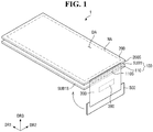
- FIG. 1 is a perspective view of a display device according to an embodiment.
- a display device 1 includes a display panel having, a printed circuit board 300 connected to one side surface of the display substrates 100 and 200, and a main circuit board 500 connected to the printed circuit board 300.
- the display panel may include a first substrate 100, a second substrate 200, various elements arranged on the first substrate 100, and various elements arranged on the second substrate 200.
- the display panel may be, for example, an organic light emitting display panel.
- an organic light emitting display panel is used as the display panel, but the present disclosure is not limited thereto.
- the display panel different kinds of display panels such as a liquid crystal display (LCD) panel, a quantum dot organic light emitting display (QD-OLED) panel, a quantum dot liquid crystal display (QT-LCD) panel, and a micro light emitting display (Micro LED) panel may be used.
- LCD liquid crystal display
- QD-OLED quantum dot organic light emitting display
- QT-LCD quantum dot liquid crystal display
- Micro LED micro light emitting display
- the various elements of the first substrate 100 may include a plurality of insulating layers, a plurality of conductive layers, at least one thin film transistor, and an organic light emitting element connected to the at least one thin film transistor.
- the first substrate 100 may be a back plate substrate including the at least one thin film transistor, or a thin film transistor substrate.
- the second substrate 200 may be disposed on the first substrate 100 to face the first substrate 100.
- the second substrate 200 may include an encapsulation substrate for encapsulating the organic light emitting element of the first substrate 100.
- Each of the first substrate 100 and the second substrate 200 may include a base substrate.
- the base substrate of each of the first substrate 100 and the second substrate 200 may include a rigid material such as glass or quartz.
- the first substrate 100 may include a first base substrate SUB 1.
- the first substrate 100 may further include a connection wiring 110 disposed between the first base substrate SUB1 and the second substrate 200.
- the display panel may have a rectangular shape having flat corners in a plan view.
- the display panel may have long sides and short sides in a plan view.
- the short sides of the display panel may be sides extending in the second direction DR2.
- the long sides of the display panel may be sides extending in the first direction DR1.
- the first substrate 100 and the second substrate 200 may have substantially the same planar shape.
- the lower short sides of the first substrate 100 and the second substrate 200 in the second direction DR2 are polished, and thus one side surface of the first substrate 100 and one side surface of the second substrate 200 may be aligned along a thickness direction (third direction DR3). In other sides of the first substrate 100 and the second substrate 200, the side surfaces of the first substrate 100 and the second substrate 200 may be aligned along the thickness direction, but the present invention is not limited thereto.
- one polished side surface 100S of the first substrate 100 and one polished side surface 200S of the second substrate 200 are referred to as a first side surface of the first substrate 100 and a second side surface of the second substrate 200, respectively.
- the first substrate 100 may include a display area DA and a non-display area NA disposed around the display area DA.
- a plurality of pixels may be disposed in the display area DA of the first substrate 100.
- the pixel may include at least one thin film transistor and an organic light emitting element.
- the non-display area NA of the first substrate 100 may further include a sealing area.
- the sealing area may be disposed in the non-display area NA, and may be continuously disposed along the edges of the first substrate 100 and the second substrate 200.
- a sealing member including a frit or the like may be disposed in the sealing area. The sealing member may be disposed between the first substrate 100 and the second substrate 200 to couple the first substrate 100 and the second substrate 200.
- the display area DA may have a rectangular shape having vertical corners or a rectangular shape having rounded corners in a plan view.
- the planar shape of the display area DA may be substantially the same as the aforementioned planar shape of the display panel 100 and 200. That is, the display area DA may have short sides and long sides.
- the long sides of the display area DA may be sides extending in the first direction DR1.
- the short sides of the display area DA may be sides extending in the second direction DR2.
- the planar shape of the display area DA is not limited to the rectangular shape, but the display area DA may have a circular shape, an elliptical shape, or other various shapes.
- the non-display area NA may be disposed around the display area DA.
- the non-display area NA may be disposed adjacent to both short sides and long sides of the display area DA.
- the non-display area NA may surround all sides of the display area DA, and may constitute edges of the display area DA.
- the present invention is not limited thereto, and the non-display area NA may be disposed adjacent only to both short sides and/or long sides of the display area DA.
- the sealing area may have a rectangular frame shape that is continuously disposed along the edge regions of the first substrate 100 and the second substrate 200.
- connection wiring 110 may extend from the display area DA of the first substrate 100 to the non-display area NA thereof (lower sides in the first direction DR1).
- the connection line 110 may be electrically connected to the pixel of the display area DA.
- the connection wiring 110 may extend to the first substrate 100 and the first side surface of the second substrate 200, and the first side surface 110s of the connection wiring 110.
- the first substrate 100, and the first side surface of the second substrate 200 may be aligned along the thickness direction.
- the first base substrate SUB1 of the first substrate 100 may include a first side surface SUB1S.
- the first side surface SUB1S of the first base substrate SUB1, the first side surface 110s of the connection wiring 110, and the first side surface of the second substrate 200 may be aligned along the thickness direction.
- connection wirings 110 may be provided.
- the plurality of connection wirings 110 may be disposed to be spaced apart from each other along the second direction DR2. Although it is shown in the drawings that five connection lines 110 are provided, six connection lines 110 may be provided.
- the connection wiring 110 may include at least one metal selected from molybdenum (Mo), aluminum (Al), platinum (Pt), palladium (Pd), silver (Ag), magnesium (Mg), gold (Au), nickel (Ni), neodymium (Nd), iridium (Ir), chromium (Cr), calcium (Ca), titanium (Ti), tantalum (Ta), tungsten (W), and copper (Cu).
- the first substrate 100 may further include a connection pad disposed on the connection wiring 110.
- the connection pad and the connection wiring 110 may be directly connected to each other.
- the connection pad may be disposed corresponding to the connection wiring 110.
- a plurality of connection pads may be provided.
- the printed circuit board 300 may be attached onto the first substrate 100 and the first side surface of the second substrate 200.
- the printed circuit board 300 may be electrically connected to the plurality of connection wirings 110 and the plurality of connection pads.
- the printed circuit board 300 may further include a driving integrated circuit 390.
- the driving integrated circuit 390 may be electrically connected to the plurality of connection wirings 110 through lead wirings to be described later.
- the printed circuit board 300 is attached only to the first side surface of the display panel, the present invention is not limited thereto, and the printed circuit board 300 may also be disposed on at least one of the first side surface of the display panel and other side surfaces thereof.
- One end of the printed circuit board 300 may be attached to the display panel 100 and 200, and the other end of the printed circuit board 300, opposite to the one end thereof, may be attached to the main circuit board 500.
- the printed circuit board 300 may be attached onto the connection pads of the first substrate 100 using an anisotropic conductive film. Thus, the lead wirings of the printed circuit board 300 may be electrically connected to the connection pads of the first substrate 100.
- the printed circuit board 300 may be a flexible printed circuit board, a printed circuit board, or a flexible film such as a chip on film.
- the driving integrated circuit 390 may be, for example, a data driving integrated circuit, and a chip on film (COF) implemented as a data driving chip may be applied.
- COF chip on film
- the main circuit board 500 may be connected to the other end of the printed circuit board 300.
- the display device 1 may further include a touch electrode unit disposed on the second substrate 200.
- the touch electrode unit may be formed directly on the second substrate 200.
- the touch electrode unit may further include touch electrodes arranged in a touch sensor area to detect a user's touch.
- the touch electrode unit may be formed as a member separately provided from the display panel 100 and 200.
- the printed circuit board 300 and the main circuit board 500 may be disposed to be bent toward the lower portion of the first substrate 100. That is, the printed circuit board 300 and the main circuit board 500 may be disposed under the first substrate 100.
- FIG. 2 is a side view of a display device according to an embodiment
- FIG. 3 is a cross-sectional view taken along the line III-III' of FIG. 2
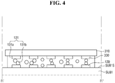
- FIG. 4 is a cross-sectional view taken along the line IV-IV' of FIG. 2
- FIG. 5 is a cross-sectional view taken along the line V-V' of FIG. 2
- FIG. 6 is a cross-sectional view taken along the line VI-VI' of FIG. 2 .
- connection pads 120 may be disposed on the first side surface SUB1S of the first base substrate SUB 1 of the first substrate 100, the first side surfaces 110s of the plurality of connection wirings 110, and the first side surface 200S of the second substrate 200.
- the connection pads 120 may be disposed to be spaced apart from each other along the second direction DR2.
- connection pads 120 may have a line shape extending along the third direction DR3.
- the connection pads 120 may be disposed to overlap the connection wirings 110 along the first direction DR1. As shown in FIG. 2 , the connection pads 120 and the connection wirings 110, corresponding to each other, may be misaligned along the second direction DR2.
- connection pads 120 may include silver (Ag), gold (Au), or copper (Cu).
- cylindrical connection pads may be formed on the first side surface SUB1S of the first base substrate SUB1 of the first substrate 100, the first side surfaces 110s of the plurality of connection wirings 110, and the first side surface 200S of the second substrate 200, which are polished.
- the cylindrical connection pads may be formed on the first side surface SUB1S of the first base substrate SUB1 of the first substrate 100, the first side surfaces 110s of the plurality of connection wirings 110, and the first side surface 200S of the second substrate 200 in the form of Ag film, Ag paste, Cu paste, or Au paste.
- the cylindrical connection pads may be formed on the first side surface SUB1S of the first base substrate SUB1 of the first substrate 100, the first side surfaces 110s of the plurality of connection wirings 110, and the first side surface 200S of the second substrate 200 by a sputtering process of depositing silver (Ag), gold (Au), or copper (Cu).
- the cylindrical connection pads may be formed into a plurality of connection pads 120 spaced apart from each other through laser patterning.
- connection pads 120 has a corresponding connection wirings 110 that should completely overlap each of the connection pads 120 along the first direction DR1. Some the connection pads 120 and their corresponding connection wirings 110 may be misaligned with each other along the second direction DR2 without completely overlapping each other along the first direction DR1.
- a coupling member 130 may be disposed between the plurality of connection pads 120 and the plurality of lead wirings 330 of the printed circuit board 300.
- the coupling member 130 includes a conductive material in an area overlapping the connection wirings 110 along the first direction DR1, a short circuit may occur due to the misalignment of the connection wirings 110 and the connection pads 120 disposed adjacent to the connection wirings 110 by the conductive material.
- a portion of the connection wiring 110, which protrudes from the connection pads 120 corresponding to the connection wiring 110 in the upper direction of the second direction DR2 may be short circuited with a portion of the adjacent connection pad 120 adjacent to the above connection pad 120, which protrudes from the connection wiring 110 corresponding to the adjacent connection pad in the lower direction of the second direction DR2 by the conductive material.
- the width of the portion protruding from the connection pad 120 corresponding to the connection wiring 110 in the upper t direction of the second direction DR2 may be about 5 ⁇ m
- the pitch of the adjacent connection pad 120 may be about 22 ⁇ m.
- the alignment tolerance may be -5 ⁇ m to +5 ⁇ m during the laser patterning process of the connection pads 120.
- the display device 1 since the display device 1 according to an embodiment includes a non-conductive film portion in which the coupling member 130 does not include a conductive material in an area where the connection pad 120 and the connection wiring 110 overlap each other along the first direction DR1, it is possible to prevent a short circuit from occurring due to a portion protruding from the connection pad 120 corresponding to the connection wiring 110 in the upper direction of the second direction DR2, a portion protruding from the connection pad 120 corresponding to the connection wiring 110 in the lower direction of the second direction DR2, and the conductive material.
- the coupling member may include a plurality of divided portions 131, 133, and 135.
- the plurality of divided portions 131, 133, and 135 may include a non-conductive portion 135 and conductive film portions disposed around the non-conductive portion 135.
- the conductive film portions may include a first conductive film portion 131 located under the non-conductive portion 135 in the third direction DR3 and a second conductive film portion 133 located over the non-conductive portion 135 in the third direction DR3.
- the non-conductive film portion 135 may be disposed to overlap the plurality of connection wirings 110 along the first direction DR1.
- the non-conductive film portion 135 may also be disposed to overlap a space between the plurality of connection wirings 110 spaced apart from each other along the second direction DR2.
- the non-conductive film portion 135 may be disposed to partially overlap the first side surface SUB1S of the first base substrate SUB1 of the first substrate 100 and the first side surface 200S of the second substrate 200 along the first direction DR1.
- the conductive film portions 131 and 133 may be disposed around the non-conductive film portion 135.
- the size of the region on the side surface of the conductive film portions 131 and 133 may be larger than the size of the region on the side surface of the non-conductive film portion 135.
- the first conductive film portion 131 may be located under the non-conductive film portion 135 in the third direction DR3, and the second conductive film portion 133 may be located over the non-conductive film portion 135 in the third direction DR3.
- the non-conductive film part 135 may be disposed between the first conductive film portion 131 and the second conductive film portion 133, and may physically connect the first conductive film portion 131 and the second conductive film portion 133.
- the conductive film portions 131 and 133 may include substantially the same material, but maybe different material from the non-conductive film portion 135.
- the planar size of the coupling member 130 may be smaller than the planar size of the printed circuit board 300, but the present invention is not limited thereto.
- connection pads 120 may be disposed on the first side surface 200S of the second substrate 200 and the first side surface SUB1S of the first base substrate SUB1 of the first substrate 100.
- the first conductive film portion 131 may include a first base bonding layer 131a and a plurality of first conductive balls 131b dispersed in the first base bonding layer 131a
- the second conductive film portion 133 may include a second base bonding layer 133a and a plurality of second conductive balls 133b dispersed in the second base bonding layer 133a.
- the first and second base bonding layers 131a and 133a may include the same material as each other.
- the first and second base bonding layers 131a and 133a may include a first insulating resin.
- the first insulating resin may have higher viscosity than a second insulating resin of a third base bonding layer 135a to be described later.
- the printed circuit board 300 may include a printed base film 310 and a plurality of lead wirings 330 disposed on the printed base film 310.
- the lead wirings 330 may be disposed on the lower surface of the printed base film 310.
- the plurality of lead wirings 330 may overlap the respective connection pads 120 along the first direction DR1.
- the connection pads 120 are disposed to completely overlap the lead wirings 330 along the first direction DR1, the connection pads 120 and the lead wirings 330 may be partially misaligned.
- the first and second conductive balls 131b and 133b may serve to electrically connect the lead wirings 330 and the connection pads 120.
- the first and second base bonding layers 131a and 133a may serve to bond the printing base film 310 and the first substrate 100, or bond the printing base film 310 and the second substrate 200.
- the first and second base bonding layers 131a and 133a may cover all the side surfaces of the lead wirings 330 and the connection pads 120 and may be in direct contact with all the side surfaces of the lead wirings 330 and the connection pads 120.
- the non-conductive film portion 135 may not include conductive balls.
- the misalignment of the connection pads 120 and the connection wirings 110, corresponding to each other, may occur along the first direction DR1.
- the coupling member 130 may include the non-conductive film portion 135 in an area overlapping the connection wirings 110 along the first direction DR1, thereby preventing a short circuit due to the misalignment of the connection wirings and the connection pads 120 adjacent to the connection wirings by the conductive material.
- the occurrence of signal interference between the adjacent wirings may be prevented, thereby reducing the failure of the display device 1.
- connection pad 120 may be disposed on the first side surface SUB1S of the first base substrate SUB1 of the first substrate 100, the first side surface 200S of the second substrate 200, and the first side surface 110s of the connection wiring 110.
- the coupling member 130 may be disposed between the connection pad 120 and the lead wiring 330.
- the non-conductive film part 135 may be disposed on the center of the connection pad 120
- the first -conductive film part 131 may be disposed under the connection pad 120 in the third direction DR3
- the second conductive film portion 133 may be disposed over the connection pad 120 in the third direction DR3.
- the coupling member 130 may be in direct contact with the connection pad 120 and the lead wiring 330.
- FIG. 7 is a side view showing a case where a material of a conductive film portion is not introduced into a non-conductive film portion from the conductive film portion
- FIG. 8 is a cross-sectional view showing a case where a material of a conductive film portion is not introduced into a non-conductive film portion from the conductive film portion.
- the third base bonding layer 135a may include a different material from the first and second base bonding layers 131a and 133a.
- the third base bonding layer 135a may include a second insulating resin different from the first insulating resin.
- the second insulating resin may have higher viscosity than the first insulating resin. That is, the viscosity of the third base bonding layer 135a may be higher than the viscosity of each of the first and second base bonding layers 131a and 133a.
- the constituent materials 131a, 131b, 133a, and 133b of the first and second conductive film portions 131 and 133 from being introduced into an area where the connection pad 120 and the connection wiring 110 are disposed to overlap each other along the first direction DR1. More specifically, when the viscosity of the third base bonding layer 135a may be higher than the viscosity of each of the first and second base bonding layers 131a and 133a, the conductive balls 131b and 133b dispersed in the first and second base bonding layers 131a and 133a may be less likely to be introduced into the third base bonding layer 135a.
- the non-conductive film portion includes the conductive balls 131b and 133b even though the conductive balls are not arranged in the third base bonding layer 135a, there is a high possibility that a short circuit occurs due to the misalignment of the connection wiring 110 corresponding to the introduced conductive balls, the connection wiring 110 disposed adjacent to the connection pad 120, and the connection pad 120.
- the third base bonding layer 135a since the third base bonding layer 135a has higher viscosity than each of the first and second base bonding layers 131a and 133a, it may reduce the possibility of the conductive balls 131b and 133b dispersed in the first and second base bonding layers 131a and 133a being introduced into the third base bonding layer 135a, preventing a short circuit.
- FIG. 9 is a perspective view of a display device according to another embodiment.
- a display device 2 according to the present embodiment is different from the aforementioned display device 1 in that a liquid crystal display panel is used as the display panel.
- the display device 2 may further include a liquid crystal layer LC between the first substrate 100 and the second substrate 200, and may further include a backlight unit BLU under the second substrate 200.
- the second substrate may include a color filter substrate including a color filter layer.
- each of the first substrate 100 and the second substrate 200 may have long sides extending along the second direction DR2 and short sides extending along the first direction DR1.
- a plurality of printed circuit boards 300 may be provided.
- the plurality of printed circuit boards 300 may be disposed on the first side surface of the first substrate 100 and the first side surface of the second substrate 200.
- the plurality of printed circuit boards 300 may be disposed to be spaced apart from each other along the second direction DR2.
- a short circuit may occur due to a portion of the connection wiring 110 protrudes from the connection pad 120 in the upper direction of the second direction DR2, a portion of the adjacent connection pad 120, which protrudes from the connection wiring 110 corresponding to the adjacent connection pad 120 in the lower direction of the second direction DR2, and the conductive material.
- the width of the portion protruding from the connection pad 120 corresponding to the connection wiring 110 in the upper direction of the second direction DR2 may be about 5 ⁇ m
- the pitch of the adjacent connection pad 120 may be about 22 ⁇ m.
- the alignment tolerance may be -5 ⁇ m to +5 ⁇ m during the laser patterning process of the connection pads 120.
- the display device 2 since the display device 2 according to an embodiment includes a non-conductive film portion 1 in an area where the connection pad 120 and the connection wiring 110 overlap each other along the first direction DR1, it is possible to prevent a short circuit due to a portion of the connection wiring 110, which protrudes from the connection pad 120 corresponding to the connection wiring 110 in the upper direction of the second direction DR2, a portion of the adjacent connection pad 120, which protrudes from the connection wiring 110 corresponding to the adjacent connection pad 120 in the lower direction of the second direction DR2, and the conductive material.
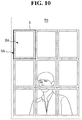
- FIG. 10 is a perspective view of a display device according to still another embodiment.
- a display device according to the present embodiment is different from the aforementioned display devices 1 and 2 of FIGS. 1 and 9 in that a tiled display device TD is used.
- a plurality of display devices 3 may be arranged in a grid form, but the present invention is not limited thereto.
- the plurality of display devices 3 may be arranged to be connected in one direction, may be arranged to be connected in a direction intersecting the one direction, or may be arranged to have a specific shape.
- the plurality of display devices 3 may have the same size as each other, but the present invention is not limited thereto.
- the plurality of display devices 3 may have different sizes from each other.
- the plurality of display devices 3 included in the tiled display device TD may be substantially the same as the display device 1 of FIG. 1 or the display device 2 of FIG. 9 . Since each of the display devices 3 has been described with reference to FIGS. 1 and 9 , a redundant description will be omitted.
- Each of the display devices 3 may be arranged such that long sides or short sides are connected to each other. Some display devices 3 may constitute one side of the tiled display device TD, some display devices 3 may be located at the edge of the tiled display device TD to constitute two adjacent sides of the tiled display device TD, and some display devices 3 may be located inside the tiled display device TD to be surround by other display devices 3.
- the plurality of display devices 3 may have different bezel shapes according to positions, and may also have the same shape as each other.
- the tiled display device TD may have a flat shape of the display devices 3, but the present invention is not limited thereto.
- the tiled display device TD may have a three-dimensional shape to provide a stereoscopic effect.
- each of the display devices 3 included in the tiled display device TD may have a curved shape, and the display devices 3 may be connected to each other in a planar shape or at a predetermined angle to form the entire tiled display device TD in a three-dimensional shape.
- a short circuit may occur due to a portion of the connection wiring 110, which protrudes from the connection pad 120 corresponding to the connection wiring 110 in the upper direction of the second direction DR2, a portion of the adjacent connection pad 120, which protrudes from the connection wiring 110 corresponding to the adjacent connection pad 120 in the lower direction of the second direction DR2, and the conductive material.
- the width of the portion protruding from the connection pad 120 corresponding to the connection wiring 110 in the upper direction of the second direction DR2 may be about 5 ⁇ m
- the pitch of the adjacent connection pad 120 may be about 22 ⁇ m.
- the alignment tolerance may be -5 ⁇ m to +5 ⁇ m during the laser patterning process of the connection pads 120.
- the display device 3 since the display device 3 according to an embodiment includes a non-conductive film portion in an area where the connection pad 120 and the connection wiring 110 overlap each other along the first direction DR1, it is possible to prevent a short circuit from occurring due to a portion of to the connection wiring 110, which protrudes from the connection pad 120 corresponding to the connection wiring 110 in the upper direction of the second direction DR2, a portion of the adjacent connection pad 120, which protrudes from the connection wiring 110 corresponding to the adjacent connection pad 120 in the lower direction of the second direction DR2, and the conductive material.
- FIG. 11 is a side view of a display device according to another embodiment
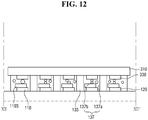
- FIG. 12 is a cross-sectional view taken along the line XII-XII' of FIG. 11 .
- the display device according to the present embodiment is different from the display device of FIG. 3 in that the arrangement of the non-conductive film portion in a coupling member 130_1 according to FIG. 11 is different from the arrangement of the non-conductive film portion in the coupling member 130 according to FIG. 2 .
- the non-conductive film portion 135 may be surrounded by a first conductive film portion 131, a second conductive film 133, and a third conductive film portion 137.
- the non-conductive film portion 135 may be disposed between the adjacent third conductive film portions, and may be disposed not to overlap the connection wiring 110, the connection pad 120, and the lead wiring 330 in the thickness direction.
- the third conductive film portion 137 may overlap the connection wiring 110, the connection pad 120, and the lead wiring 330 in the thickness direction.
- the first conductive film portion 131 may be disposed under the third conductive film portion 137 in the third direction DR3, and the second conductive film portion 133 may be disposed over the third conductive film portion 137 in the third direction DR3.
- the third conductive film portion 137 may include a fourth base bonding layer 137a and third conductive balls 137b.
- the lead wiring 330 may be electrically connected to the connection pad 120 by the third conductive balls 137b.
- a short circuit may occur due to a portion of the connection wiring 110, which protrudes from the connection pad 120 corresponding to the connection wiring 110 in the upper t direction of the second direction DR2, a portion of the adjacent connection pad 120, which protrudes from the connection wiring 110 corresponding to the adjacent connection pad 120 in the upper direction of the second direction DR2, and the conductive material.
- the width of the portion protruding from the connection pad 120 corresponding to the connection wiring 110 in the right direction of the second direction DR2 may be about 5 ⁇ m
- the pitch of the adjacent connection pad 120 may be about 22 ⁇ m.
- the alignment tolerance may be -5 ⁇ m to +5 ⁇ m during the laser patterning process of the connection pads 120.
- the display device further includes the third conductive film portion 137 in an area where the connection pad 120 and the connection wiring 110 are disposed to overlap each other along the first direction DR1, the adhesion force between the printed circuit board 300 and the display panel 100 and 200 may increase. Further, since this display device includes the non-conductive film portion 135 disposed between the adjacent third conductive film portions 137, it is possible to prevent a short circuit from occurring due to a portion protruding from the connection pad 120 corresponding to the connection wiring 110 in the upper direction of the second direction DR2, a portion protruding from the connection pad 120 corresponding to the connection wiring 110 in the left direction of the second direction DR2, and the conductive material.
- the fourth base bonding layer 137a may include a material different from the constituent material of the third base bonding layer 135a of the aforementioned non-conductive film portion 135.
- the fourth base bonding layer 137a includes the same material as the first base bonding layer 131a, thereby including an insulating resin having lower viscosity than the third base bonding layer 135a.
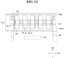
- FIG. 13 is a side view of a display device according to still another embodiment
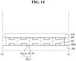
- FIG. 14 is a cross-sectional view taken along the line XIV-XIV' of FIG. 13 .
- a display device is different from the aforementioned display device in that a non-conductive film portion 135_2 of a coupling member 130_2 includes portions having different widths from each other in the thickness direction.
- the non-conductive film portion 135_2 may include a first sub non-conductive film portion 135_2a disposed to overlap the connection wiring 110 along the first direction DR1, and a second sub non-conductive film portion 135_2b disposed not to overlap the connection wiring 110 along the first direction DR1.
- the first sub nonconductive film portions 135_2a and the second sub nonconductive film portions 135_2b may be alternately arranged along the second direction DR2.
- the first sub-nonconductive film portion 135_2a may have a shape protruding more upwardly and downwardly from the second sub-conductive film portion 135_2b in the third direction DR3.
- a short circuit may occur due to a portion of the connection wiring 110, which protrudes from the connection pad 120 corresponding to the connection wiring 110 in the upper direction of the second direction DR2, a portion of the adjacent connection pad 120, which protrudes from the connection wiring 110 corresponding to the adjacent connection pad 120 in the upper direction of the second direction DR2, and the conductive material.
- the width of the portion protruding from the connection pad 120 corresponding to the connection wiring 110 in the upper direction of the second direction DR2 may be about 5 ⁇ m
- the pitch of the adjacent connection pad 120 may be about 22 ⁇ m.
- the alignment tolerance may be -5 ⁇ m to +5 ⁇ m during the laser patterning process of the connection pads 120.
- the display device 2 since the display device 2 according to an embodiment includes a non-conductive film portion in an area where the connection pad 120 and the connection wiring 110 overlap each other along the first direction DR1, it is possible to prevent a short circuit from occurring due to a portion of the connection wiring 110, which protrudes from the connection pad 120 corresponding to the connection wiring 110 in the upper t direction of the second direction DR2, a portion of the adjacent connection pad 120, which protrudes from connection wiring 110 corresponding to the adjacent connection pad 120 in the lower direction of the second direction DR2, and the conductive material.
- FIG. 15 is a side view of a display device according to still another embodiment
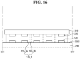
- FIG. 16 is a cross-sectional view taken along the line XVI-XVI' of FIG. 15 .
- a display device is different from the aforementioned display device in that a non-conductive film portion 135_3 of a coupling member 130_3 includes portions having different widths from each other in the thickness direction.
- the non-conductive film portion 135_3 may include a first sub non-conductive film portion 135_3a disposed to overlap the connection wiring 110 along the first direction DR1, and a second sub non-conductive film portion 135_3b disposed not to overlap the connection wiring 110 along the first direction DR1.
- the first sub nonconductive film portions 135_3a and the second sub nonconductive film portions 135_3b may be alternately arranged along the second direction DR2.
- the first sub-nonconductive film portion 135_3a may have a shape indented more upwardly and downwardly from the second sub-conductive film portion 135_3b in the third direction DR3.
- a short circuit may occur due to a portion of the connection wiring 110, which protrudes from the connection pad 120 corresponding to the connection wiring 110 in the upper direction of the second direction DR2, a portion of the adjacent connection pad 120, which protrudes from the connection wiring 110 corresponding to the adjacent connection pad 120 in the upper direction of the second direction DR2, and the conductive material.
- the width of the portion protruding from the connection pad 120 corresponding to the connection wiring 110 in the upper direction of the second direction DR2 may be about 5 ⁇ m
- the pitch of the adjacent connection pad 120 may be about 22 ⁇ m.
- the alignment tolerance may be -5 ⁇ m to +5 ⁇ m during the laser patterning process of the connection pads 120.
- the display device 2 since the display device 2 according to an embodiment includes a non-conductive film in an area where the connection pad 120 and the connection wiring 110 overlap each other along the first direction DR1, it is possible to prevent the above mentioned short circuit from occurring.
- the display device can prevent signal interference due to the misalignment of connection wirings and connection pads.
Landscapes
- Physics & Mathematics (AREA)
- Nonlinear Science (AREA)
- Engineering & Computer Science (AREA)
- General Physics & Mathematics (AREA)
- Mathematical Physics (AREA)
- Crystallography & Structural Chemistry (AREA)
- Chemical & Material Sciences (AREA)
- Optics & Photonics (AREA)
- Microelectronics & Electronic Packaging (AREA)
- Manufacturing & Machinery (AREA)
- Devices For Indicating Variable Information By Combining Individual Elements (AREA)
- Computer Hardware Design (AREA)
- Theoretical Computer Science (AREA)
- Electroluminescent Light Sources (AREA)
Abstract
Description
- Exemplary embodiments/implementations of the invention relate generally to a display device and, more specifically, to a display device that minimize a non-display area.
- A display device is a device that shows a moving image or a still image. The display device may be used as a display screen of not only portable electronic appliances such as a mobile phone, a smart phone, a tablet personal computer (PC), a smart watch, a watch phone, a mobile communication terminal, an electronic notebook, an electronic book, a portable multimedia player (PMP), a navigator, and a ultra mobile PC (UMPC), but also various products such as a television, a notebook, a monitor, a billboard, and the Internet of Things (IoT).
- In order to drive the light emitting element of a display device, a printed circuit board including a driving circuit, a plurality of signal wirings electrically connected to the light emitting element, and a plurality of lead wirings connected to the plurality of signal wirings is required. The display device includes a display area that shows an image, and a non-display area that surrounds the display area but does not present an image, that is, a bezel area. In this case, in order to make a display device without a bezel area, the signal wirings and the lead wirings may be bonded to each other at the side of the display device.
- The above information disclosed in this Background section is only for understanding of the background of the inventive concepts, and, therefore, it may contain information that does not constitute prior art.
- Devices constructed/methods according to exemplary implementations /embodiments of the invention are capable of preventing signal interference due to misalignment of connection wirings and connection pads.
- According to one or more implementations/embodiments of the invention, , a display device includes a first substrate including a display area including pixels, a non-display area disposed around the display area, and a base substrate, a second substrate facing the first substrate, and a printed circuit board attached to side surfaces of the first substrate and the second substrate, wherein the first substrate includes a plurality of connection wirings connected to the pixels, arranged on the base substrate, extending along a first direction, and spaced apart from each other along a second direction intersecting the first direction, and a plurality of connection pads arranged on the side surface of the first substrate and the side surface of the second substrate, connected to the connection wirings, extending along a thickness direction, and spaced apart from each other along the second direction, the first substrate further includes a coupling member disposed between the printed circuit board and the side surface of the first substrate and between the printed circuit board and the side surface of the second substrate, and the coupling member includes a non-conductive film portion disposed to overlap the connection wirings along the first direction, and a conductive film portion disposed around the non-conductive film portion. The non-conductive film portion does not include conductive material.
- The connection pad may be directly connected to the connection wiring. That is, there is no further element between the connection pad and the connection wiring.
- The connection pad may be partially misaligned with the connection wiring along the second direction.
- The conductive film portion may be disposed not to overlap the connection wiring along the first direction.
- The conductive film portion may include a first base layer and conductive balls dispersed in the first base bonding layer.
- The printed circuit board may include a lead wiring disposed to overlap the connection pad along the first direction, and the lead wiring may be electrically connected to the connection pad through the conductive balls.
- The non-conductive film portion may include a second base bonding layer.
- The viscosity of the second base bonding layer may be higher than the viscosity of the first base bonding layer.
- The conductive film portion may include a first conductive film portion disposed at one side of the non-conductive film portion in the thickness direction, and a second conductive film portion disposed at the other side of the non-conductive film portion in the thickness direction.
- The first conductive film portion may be disposed to overlap the base substrate along the first direction, and the second conductive film portion may be disposed to overlap the second substrate along the first direction.
- The connection wiring may include Ti/Al/Ti or Mo, and the connection pad may include Ag, Au, or Cu.
- The display device may further include: a main circuit board connected to the printed circuit board, wherein the printed circuit board may further include a data driving integrated circuit.
- The first substrate may include a thin film transistor substrate, and the second substrate may include an encapsulation substrate.
- The display device may further include a liquid crystal layer disposed between the first substrate and the second substrate, and a backlight unit disposed under the first substrate.
- The conductive film may surround the non-conductive film portion in a plan view.
- The non-conductive film portion may include a first non-conductive film portion disposed to overlap the connection wiring along the first direction, and a second non-conductive film portion disposed not to overlap the connection wiring along the first direction, and the first non-conductive film portion may protrude from the second non-conductive film portion in a thickness direction.
- The non-conductive film portion may include a first non-conductive film portion disposed to overlap the connection wiring along the first direction, and a second non-conductive film portion disposed not to overlap the connection wiring along the first direction, and the second non-conductive film portion may protrude from the first non-conductive film portion in a thickness direction.
- According to another embodiment, a display device includes a first substrate including a display area including pixels, a non-display area disposed around the display area, and a base substrate, and a second substrate facing the first substrate, wherein the first substrate includes a connection wiring connected to the pixels, disposed on the base substrate, and extending along a first direction, and a connection pad disposed on the side surface of the first substrate and the side surface of the second substrate, connected to the connection wiring, and extending along a thickness direction, the first substrate further includes a coupling member disposed on the side surface of the first substrate and the side surface of the second substrate, the coupling member includes a non-conductive film portion disposed to overlap the connection wirings along the first direction, and a conductive film portion disposed around the non-conductive film portion, the conductive film portion includes a first base bonding layer and conductive balls dispersed in the first base bonding layer, the non-conductive film portion includes a second base bonding layer, and viscosity of the second base bonding layer is higher than viscosity of the first base bonding layer.
- The display device may further include a printed circuit board attached to side surfaces of the first substrate and the second substrate, wherein the coupling member is disposed between the printed circuit board and the side surface of the first substrate and between the printed circuit board and the side surface of the second substrate.
- The printed circuit board may include a lead wiring disposed to overlap the connection pad along the first direction, and the lead wiring may be electrically connected to the connection pad through the conductive balls.
- Additional features of the inventive concepts will be set forth in the description which follows, and in part will be apparent from the description, or may be learned by practice of the inventive concepts.
- It is to be understood that both the foregoing general description and the following detailed description are exemplary and explanatory and are intended to provide further explanation of the invention as claimed.
- The accompanying drawings, which are included to provide a further understanding of the invention and are incorporated in and constitute a part of this specification, illustrate exemplary embodiments of the invention, and together with the description serve to explain the inventive concepts.
-
FIG. 1 is a perspective view of a display device constructed according to an exemplary embodiment of the invention. -
FIG. 2 is a side view of a display device constructed according to an exemplary embodiment of the invention. -
FIG. 3 is a cross-sectional view taken along the line III-III' ofFIG. 2 . -
FIG. 4 is a cross-sectional view taken along the line IV-IV' ofFIG. 2 . -
FIG. 5 is a cross-sectional view taken along the line V-V' ofFIG. 2 . -
FIG. 6 is a cross-sectional view taken along the line VI-VI' ofFIG. 2 . -
FIG. 7 is a side view showing a case where a material of a conductive film portion is not introduced into a non-conductive film portion from the conductive film portion. -
FIG. 8 is a cross-sectional view showing a case where a material of a conductive film portion is not introduced into a non-conductive film portion from the conductive film portion. -
FIG. 9 is a perspective view of a display device constructed according to another exemplary embodiment of the invention. -
FIG. 10 is a perspective view of a display device constructed according to still another exemplary embodiment of the invention. -
FIG. 11 is a side view of a display device constructed according to another exemplary embodiment of the invention. -
FIG. 12 is a cross-sectional view taken along the line XII-XII' ofFIG. 11 . -
FIG. 13 is a side view of a display device constructed according to still another exemplary embodiment of the invention. -
FIG. 14 is a cross-sectional view taken along the line XIV-XIV' ofFIG. 13 . -
FIG. 15 is a side view of a display device constructed according to still another exemplary embodiment of the invention. -
FIG. 16 is a cross-sectional view taken along the line XVI-XVI' ofFIG. 15 . - In the following description, for the purposes of explanation, numerous specific details are set forth in order to provide a thorough understanding of various exemplary embodiments or implementations of the invention. As used herein "embodiments" and "implementations" are interchangeable words that are non-limiting examples of devices or methods employing one or more of the inventive concepts disclosed herein. It is apparent, however, that various exemplary embodiments may be practiced without these specific details or with one or more equivalent arrangements. In other instances, well-known structures and devices are shown in block diagram form in order to avoid unnecessarily obscuring various exemplary embodiments. Further, various exemplary embodiments may be different, but do not have to be exclusive. For example, specific shapes, configurations, and characteristics of an exemplary embodiment may be used or implemented in another exemplary embodiment without departing from the inventive concepts.
- Unless otherwise specified, the illustrated exemplary embodiments are to be understood as providing exemplary features of varying detail of some ways in which the inventive concepts may be implemented in practice. Therefore, unless otherwise specified, the features, components, modules, layers, films, panels, regions, and/or aspects, etc. (hereinafter individually or collectively referred to as "elements"), of the various embodiments may be otherwise combined, separated, interchanged, and/or rearranged without departing from the inventive concepts.
- The use of cross-hatching and/or shading in the accompanying drawings is generally provided to clarify boundaries between adjacent elements. As such, neither the presence nor the absence of cross-hatching or shading conveys or indicates any preference or requirement for particular materials, material properties, dimensions, proportions, commonalities between illustrated elements, and/or any other characteristic, attribute, property, etc., of the elements, unless specified. Further, in the accompanying drawings, the size and relative sizes of elements may be exaggerated for clarity and/or descriptive purposes. When an exemplary embodiment may be implemented differently, a specific process order may be performed differently from the described order. For example, two consecutively described processes may be performed substantially at the same time or performed in an order opposite to the described order. Also, like reference numerals denote like elements.
- When an element, such as a layer, is referred to as being "on," "connected to," or "coupled to" another element or layer, it may be directly on, connected to, or coupled to the other element or layer or intervening elements or layers may be present. When, however, an element or layer is referred to as being "directly on," "directly connected to," or "directly coupled to" another element or layer, there are no intervening elements or layers present. To this end, the term "connected" may refer to physical, electrical, and/or fluid connection, with or without intervening elements. Further, the D1-axis, the D2-axis, and the D3-axis are not limited to three axes of a rectangular coordinate system, such as the x, y, and z - axes, and may be interpreted in a broader sense. For example, the D1-axis, the D2-axis, and the D3-axis may be perpendicular to one another, or may represent different directions that are not perpendicular to one another. For the purposes of this disclosure, "at least one of X, Y, and Z" and "at least one selected from the group consisting of X, Y, and Z" may be construed as X only, Y only, Z only, or any combination of two or more of X, Y, and Z, such as, for instance, XYZ, XYY, YZ, and ZZ. As used herein, the term "and/or" includes any and all combinations of one or more of the associated listed items.
- Although the terms "first," "second," etc. may be used herein to describe various types of elements, these elements should not be limited by these terms. These terms are used to distinguish one element from another element. Thus, a first element discussed below could be termed a second element without departing from the teachings of the disclosure.
- Spatially relative terms, such as "beneath," "below," "under," "lower," "above," "upper," "over," "higher," "side" (e.g., as in "sidewall"), and the like, may be used herein for descriptive purposes, and, thereby, to describe one elements relationship to another element(s) as illustrated in the drawings. Spatially relative terms are intended to encompass different orientations of an apparatus in use, operation, and/or manufacture in addition to the orientation depicted in the drawings. For example, if the apparatus in the drawings is turned over, elements described as "below" or "beneath" other elements or features would then be oriented "above" the other elements or features. Thus, the exemplary term "below" can encompass both an orientation of above and below. Furthermore, the apparatus may be otherwise oriented (e.g., rotated 90 degrees or at other orientations), and, as such, the spatially relative descriptors used herein interpreted accordingly.
- The terminology used herein is for the purpose of describing particular embodiments and is not intended to be limiting. As used herein, the singular forms, "a," "an," and "the" are intended to include the plural forms as well, unless the context clearly indicates otherwise. Moreover, the terms "comprises," "comprising," "includes," and/or "including," when used in this specification, specify the presence of stated features, integers, steps, operations, elements, components, and/or groups thereof, but do not preclude the presence or addition of one or more other features, integers, steps, operations, elements, components, and/or groups thereof. It is also noted that, as used herein, the terms "substantially," "about," and other similar terms, are used as terms of approximation and not as terms of degree, and, as such, are utilized to account for inherent deviations in measured, calculated, and/or provided values that would be recognized by one of ordinary skill in the art.
- Various exemplary embodiments are described herein with reference to sectional and/or exploded illustrations that are schematic illustrations of idealized exemplary embodiments and/or intermediate structures. As such, variations from the shapes of the illustrations as a result, for example, of manufacturing techniques and/or tolerances, are to be expected. Thus, exemplary embodiments disclosed herein should not necessarily be construed as limited to the particular illustrated shapes of regions, but are to include deviations in shapes that result from, for instance, manufacturing. In this manner, regions illustrated in the drawings may be schematic in nature and the shapes of these regions may not reflect actual shapes of regions of a device and, as such, are not necessarily intended to be limiting. Unless otherwise defined, all terms (including technical and scientific terms) used herein have the same meaning as commonly understood by one of ordinary skill in the art to which this disclosure is a part. Terms, such as those defined in commonly used dictionaries, should be interpreted as having a meaning that is consistent with their meaning in the context of the relevant art and should not be interpreted in an idealized or overly formal sense, unless expressly so defined herein.
- Exemplary embodiments are described herein with reference to cross section illustrations that are schematic illustrations of idealized embodiments. As such, variations from the shapes of the illustrations as a result, for example, of manufacturing techniques and/or tolerances, are to be expected. Thus, embodiments described herein should not be construed as limited to the particular shapes of regions as illustrated herein but are to include deviations in shapes that result, for example, from manufacturing. For example, a region illustrated or described as flat may, typically, have rough and/or nonlinear features. Moreover, sharp angles that are illustrated may be rounded. Thus, the regions illustrated in the figures are schematic in nature and their shapes are not intended to illustrate the precise shape of a region and are not intended to limit the scope of the present claims.
- Hereinafter, embodiments of the invention will be described with reference to the attached drawings.
-
FIG. 1 is a perspective view of a display device according to an embodiment. - Referring to
FIG. 1 , adisplay device 1 includes a display panel having, a printedcircuit board 300 connected to one side surface of thedisplay substrates main circuit board 500 connected to the printedcircuit board 300. - The display panel may include a
first substrate 100, asecond substrate 200, various elements arranged on thefirst substrate 100, and various elements arranged on thesecond substrate 200. - The display panel may be, for example, an organic light emitting display panel. In the following embodiments, there is exemplified a case where an organic light emitting display panel is used as the display panel, but the present disclosure is not limited thereto. For example, as the display panel, different kinds of display panels such as a liquid crystal display (LCD) panel, a quantum dot organic light emitting display (QD-OLED) panel, a quantum dot liquid crystal display (QT-LCD) panel, and a micro light emitting display (Micro LED) panel may be used.
- The various elements of the
first substrate 100 may include a plurality of insulating layers, a plurality of conductive layers, at least one thin film transistor, and an organic light emitting element connected to the at least one thin film transistor. - That is, the
first substrate 100 may be a back plate substrate including the at least one thin film transistor, or a thin film transistor substrate. - The
second substrate 200 may be disposed on thefirst substrate 100 to face thefirst substrate 100. Thesecond substrate 200 may include an encapsulation substrate for encapsulating the organic light emitting element of thefirst substrate 100. - Each of the
first substrate 100 and thesecond substrate 200 may include a base substrate. The base substrate of each of thefirst substrate 100 and thesecond substrate 200 may include a rigid material such as glass or quartz. For example, thefirst substrate 100 may include a firstbase substrate SUB 1. - The
first substrate 100 may further include aconnection wiring 110 disposed between the first base substrate SUB1 and thesecond substrate 200. - The display panel may have a rectangular shape having flat corners in a plan view. The display panel may have long sides and short sides in a plan view. The short sides of the display panel may be sides extending in the second direction DR2. The long sides of the display panel may be sides extending in the first direction DR1. The
first substrate 100 and thesecond substrate 200 may have substantially the same planar shape. - The lower short sides of the
first substrate 100 and thesecond substrate 200 in the second direction DR2 are polished, and thus one side surface of thefirst substrate 100 and one side surface of thesecond substrate 200 may be aligned along a thickness direction (third direction DR3). In other sides of thefirst substrate 100 and thesecond substrate 200, the side surfaces of thefirst substrate 100 and thesecond substrate 200 may be aligned along the thickness direction, but the present invention is not limited thereto. - Hereinafter, one polished side surface 100S of the
first substrate 100 and onepolished side surface 200S of thesecond substrate 200 are referred to as a first side surface of thefirst substrate 100 and a second side surface of thesecond substrate 200, respectively. - The
first substrate 100 may include a display area DA and a non-display area NA disposed around the display area DA. A plurality of pixels may be disposed in the display area DA of thefirst substrate 100. The pixel may include at least one thin film transistor and an organic light emitting element. Although not shown, the non-display area NA of thefirst substrate 100 may further include a sealing area. The sealing area may be disposed in the non-display area NA, and may be continuously disposed along the edges of thefirst substrate 100 and thesecond substrate 200. A sealing member including a frit or the like may be disposed in the sealing area. The sealing member may be disposed between thefirst substrate 100 and thesecond substrate 200 to couple thefirst substrate 100 and thesecond substrate 200. - The display area DA may have a rectangular shape having vertical corners or a rectangular shape having rounded corners in a plan view. The planar shape of the display area DA may be substantially the same as the aforementioned planar shape of the
display panel - The non-display area NA may be disposed around the display area DA. The non-display area NA may be disposed adjacent to both short sides and long sides of the display area DA. In this case, the non-display area NA may surround all sides of the display area DA, and may constitute edges of the display area DA. However, the present invention is not limited thereto, and the non-display area NA may be disposed adjacent only to both short sides and/or long sides of the display area DA.
- The sealing area may have a rectangular frame shape that is continuously disposed along the edge regions of the
first substrate 100 and thesecond substrate 200. - The
connection wiring 110 may extend from the display area DA of thefirst substrate 100 to the non-display area NA thereof (lower sides in the first direction DR1). Theconnection line 110 may be electrically connected to the pixel of the display area DA. Theconnection wiring 110 may extend to thefirst substrate 100 and the first side surface of thesecond substrate 200, and the first side surface 110s of theconnection wiring 110. Thefirst substrate 100, and the first side surface of thesecond substrate 200 may be aligned along the thickness direction. - The first base substrate SUB1 of the
first substrate 100, like the first side surface of thefirst substrate 100, may include a first side surface SUB1S. The first side surface SUB1S of the first base substrate SUB1, the first side surface 110s of theconnection wiring 110, and the first side surface of thesecond substrate 200 may be aligned along the thickness direction. - A plurality of
connection wirings 110 may be provided. The plurality ofconnection wirings 110 may be disposed to be spaced apart from each other along the second direction DR2. Although it is shown in the drawings that fiveconnection lines 110 are provided, sixconnection lines 110 may be provided. - The
connection wiring 110 may include at least one metal selected from molybdenum (Mo), aluminum (Al), platinum (Pt), palladium (Pd), silver (Ag), magnesium (Mg), gold (Au), nickel (Ni), neodymium (Nd), iridium (Ir), chromium (Cr), calcium (Ca), titanium (Ti), tantalum (Ta), tungsten (W), and copper (Cu). - The
first substrate 100 may further include a connection pad disposed on theconnection wiring 110. The connection pad and theconnection wiring 110 may be directly connected to each other. The connection pad may be disposed corresponding to theconnection wiring 110. A plurality of connection pads may be provided. - The printed
circuit board 300 may be attached onto thefirst substrate 100 and the first side surface of thesecond substrate 200. The printedcircuit board 300 may be electrically connected to the plurality ofconnection wirings 110 and the plurality of connection pads. - The printed
circuit board 300 may further include a drivingintegrated circuit 390. The drivingintegrated circuit 390 may be electrically connected to the plurality ofconnection wirings 110 through lead wirings to be described later. - Although it is shown in
FIG. 1 that the printedcircuit board 300 is attached only to the first side surface of the display panel, the present invention is not limited thereto, and the printedcircuit board 300 may also be disposed on at least one of the first side surface of the display panel and other side surfaces thereof. - One end of the printed
circuit board 300 may be attached to thedisplay panel circuit board 300, opposite to the one end thereof, may be attached to themain circuit board 500. - The printed
circuit board 300 may be attached onto the connection pads of thefirst substrate 100 using an anisotropic conductive film. Thus, the lead wirings of the printedcircuit board 300 may be electrically connected to the connection pads of thefirst substrate 100. The printedcircuit board 300 may be a flexible printed circuit board, a printed circuit board, or a flexible film such as a chip on film. - The driving
integrated circuit 390 may be, for example, a data driving integrated circuit, and a chip on film (COF) implemented as a data driving chip may be applied. - The
main circuit board 500 may be connected to the other end of the printedcircuit board 300. - Although not shown, the
display device 1 may further include a touch electrode unit disposed on thesecond substrate 200. The touch electrode unit may be formed directly on thesecond substrate 200. - The touch electrode unit may further include touch electrodes arranged in a touch sensor area to detect a user's touch.
- However, the present invention is not limited thereto, and the touch electrode unit may be formed as a member separately provided from the
display panel - As shown in
FIG. 1 , the printedcircuit board 300 and themain circuit board 500 may be disposed to be bent toward the lower portion of thefirst substrate 100. That is, the printedcircuit board 300 and themain circuit board 500 may be disposed under thefirst substrate 100. -
FIG. 2 is a side view of a display device according to an embodiment,FIG. 3 is a cross-sectional view taken along the line III-III' ofFIG. 2 ,FIG. 4 is a cross-sectional view taken along the line IV-IV' ofFIG. 2 ,FIG. 5 is a cross-sectional view taken along the line V-V' ofFIG. 2 , andFIG. 6 is a cross-sectional view taken along the line VI-VI' ofFIG. 2 . - Referring to
FIGS. 2 to 6 , theconnection pads 120 may be disposed on the first side surface SUB1S of the firstbase substrate SUB 1 of thefirst substrate 100, the first side surfaces 110s of the plurality ofconnection wirings 110, and thefirst side surface 200S of thesecond substrate 200. Theconnection pads 120 may be disposed to be spaced apart from each other along the second direction DR2. - The
connection pads 120 may have a line shape extending along the third direction DR3. Theconnection pads 120 may be disposed to overlap the connection wirings 110 along the first direction DR1. As shown inFIG. 2 , theconnection pads 120 and theconnection wirings 110, corresponding to each other, may be misaligned along the second direction DR2. - The
connection pads 120 may include silver (Ag), gold (Au), or copper (Cu). - More specifically, cylindrical connection pads may be formed on the first side surface SUB1S of the first base substrate SUB1 of the
first substrate 100, the first side surfaces 110s of the plurality ofconnection wirings 110, and thefirst side surface 200S of thesecond substrate 200, which are polished. The cylindrical connection pads may be formed on the first side surface SUB1S of the first base substrate SUB1 of thefirst substrate 100, the first side surfaces 110s of the plurality ofconnection wirings 110, and thefirst side surface 200S of thesecond substrate 200 in the form of Ag film, Ag paste, Cu paste, or Au paste. - However, the present invention is not limited thereto, and the cylindrical connection pads may be formed on the first side surface SUB1S of the first base substrate SUB1 of the
first substrate 100, the first side surfaces 110s of the plurality ofconnection wirings 110, and thefirst side surface 200S of thesecond substrate 200 by a sputtering process of depositing silver (Ag), gold (Au), or copper (Cu). - Subsequently, as shown in
FIG. 2 , the cylindrical connection pads may be formed into a plurality ofconnection pads 120 spaced apart from each other through laser patterning. - Each of the
connection pads 120 has acorresponding connection wirings 110 that should completely overlap each of theconnection pads 120 along the first direction DR1. Some theconnection pads 120 and their corresponding connection wirings 110 may be misaligned with each other along the second direction DR2 without completely overlapping each other along the first direction DR1. - A
coupling member 130 may be disposed between the plurality ofconnection pads 120 and the plurality oflead wirings 330 of the printedcircuit board 300. When thecoupling member 130 includes a conductive material in an area overlapping the connection wirings 110 along the first direction DR1, a short circuit may occur due to the misalignment of theconnection wirings 110 and theconnection pads 120 disposed adjacent to the connection wirings 110 by the conductive material. - Specifically, as shown in
FIG. 2 , a portion of theconnection wiring 110, which protrudes from theconnection pads 120 corresponding to theconnection wiring 110 in the upper direction of the second direction DR2 may be short circuited with a portion of theadjacent connection pad 120 adjacent to theabove connection pad 120, which protrudes from theconnection wiring 110 corresponding to the adjacent connection pad in the lower direction of the second direction DR2 by the conductive material. For example, the width of the portion protruding from theconnection pad 120 corresponding to theconnection wiring 110 in the upper t direction of the second direction DR2 may be about 5 µm, and the pitch of theadjacent connection pad 120 may be about 22 µm. In the misalignment of thecorresponding connection wiring 110, theconnection wiring 110 disposed adjacent to theconnection pad 120, and theconnection pad 120, the alignment tolerance may be -5 µm to +5 µm during the laser patterning process of theconnection pads 120. - In this case, signal interference may cause the
display device 1 failure. However, since thedisplay device 1 according to an embodiment includes a non-conductive film portion in which thecoupling member 130 does not include a conductive material in an area where theconnection pad 120 and theconnection wiring 110 overlap each other along the first direction DR1, it is possible to prevent a short circuit from occurring due to a portion protruding from theconnection pad 120 corresponding to theconnection wiring 110 in the upper direction of the second direction DR2, a portion protruding from theconnection pad 120 corresponding to theconnection wiring 110 in the lower direction of the second direction DR2, and the conductive material. - As shown in
FIG. 2 , the coupling member may include a plurality of dividedportions portions non-conductive portion 135 and conductive film portions disposed around thenon-conductive portion 135. The conductive film portions may include a firstconductive film portion 131 located under thenon-conductive portion 135 in the third direction DR3 and a secondconductive film portion 133 located over thenon-conductive portion 135 in the third direction DR3. - The
non-conductive film portion 135 may be disposed to overlap the plurality ofconnection wirings 110 along the first direction DR1. Thenon-conductive film portion 135 may also be disposed to overlap a space between the plurality ofconnection wirings 110 spaced apart from each other along the second direction DR2. - The
non-conductive film portion 135 may be disposed to partially overlap the first side surface SUB1S of the first base substrate SUB1 of thefirst substrate 100 and thefirst side surface 200S of thesecond substrate 200 along the first direction DR1. - The
conductive film portions non-conductive film portion 135. The size of the region on the side surface of theconductive film portions non-conductive film portion 135. - The first
conductive film portion 131 may be located under thenon-conductive film portion 135 in the third direction DR3, and the secondconductive film portion 133 may be located over thenon-conductive film portion 135 in the third direction DR3. - The
non-conductive film part 135 may be disposed between the firstconductive film portion 131 and the secondconductive film portion 133, and may physically connect the firstconductive film portion 131 and the secondconductive film portion 133. - The
conductive film portions non-conductive film portion 135. - The planar size of the
coupling member 130 may be smaller than the planar size of the printedcircuit board 300, but the present invention is not limited thereto. - As shown in
FIGS. 3 and4 , theconnection pads 120 may be disposed on thefirst side surface 200S of thesecond substrate 200 and the first side surface SUB1S of the first base substrate SUB1 of thefirst substrate 100. The firstconductive film portion 131 may include a firstbase bonding layer 131a and a plurality of firstconductive balls 131b dispersed in the firstbase bonding layer 131a, and the secondconductive film portion 133 may include a secondbase bonding layer 133a and a plurality of secondconductive balls 133b dispersed in the secondbase bonding layer 133a. The first and secondbase bonding layers base bonding layers - The printed
circuit board 300 may include a printedbase film 310 and a plurality oflead wirings 330 disposed on the printedbase film 310. The lead wirings 330 may be disposed on the lower surface of the printedbase film 310. As shown inFIG. 2 , the plurality oflead wirings 330 may overlap therespective connection pads 120 along the first direction DR1. Although it is shown inFIG. 2 that theconnection pads 120 are disposed to completely overlap the lead wirings 330 along the first direction DR1, theconnection pads 120 and the lead wirings 330 may be partially misaligned. - Referring to
FIGS. 3 and4 , the first and secondconductive balls connection pads 120. The first and secondbase bonding layers printing base film 310 and thefirst substrate 100, or bond theprinting base film 310 and thesecond substrate 200. The first and secondbase bonding layers connection pads 120 and may be in direct contact with all the side surfaces of the lead wirings 330 and theconnection pads 120. - Unlike the
conductive film portions non-conductive film portion 135 may not include conductive balls. As described above, the misalignment of theconnection pads 120 and theconnection wirings 110, corresponding to each other, may occur along the first direction DR1. In this case, thecoupling member 130 according to an embodiment may include thenon-conductive film portion 135 in an area overlapping the connection wirings 110 along the first direction DR1, thereby preventing a short circuit due to the misalignment of the connection wirings and theconnection pads 120 adjacent to the connection wirings by the conductive material. Thus, the occurrence of signal interference between the adjacent wirings may be prevented, thereby reducing the failure of thedisplay device 1. - Referring to
FIG. 6 , theconnection pad 120 may be disposed on the first side surface SUB1S of the first base substrate SUB1 of thefirst substrate 100, thefirst side surface 200S of thesecond substrate 200, and the first side surface 110s of theconnection wiring 110. Thecoupling member 130 may be disposed between theconnection pad 120 and thelead wiring 330. In the drawings, thenon-conductive film part 135 may be disposed on the center of theconnection pad 120, the first -conductive film part 131 may be disposed under theconnection pad 120 in the third direction DR3, and the secondconductive film portion 133 may be disposed over theconnection pad 120 in the third direction DR3. Thecoupling member 130 may be in direct contact with theconnection pad 120 and thelead wiring 330. -
FIG. 7 is a side view showing a case where a material of a conductive film portion is not introduced into a non-conductive film portion from the conductive film portion, andFIG. 8 is a cross-sectional view showing a case where a material of a conductive film portion is not introduced into a non-conductive film portion from the conductive film portion. - Referring to
FIGS. 7 and8 , as described above, the third base bonding layer 135a may include a different material from the first and secondbase bonding layers base bonding layers - Thus, it is possible to prevent the
constituent materials conductive film portions connection pad 120 and theconnection wiring 110 are disposed to overlap each other along the first direction DR1. More specifically, when the viscosity of the third base bonding layer 135a may be higher than the viscosity of each of the first and secondbase bonding layers conductive balls base bonding layers conductive balls base bonding layers conductive balls connection wiring 110 corresponding to the introduced conductive balls, theconnection wiring 110 disposed adjacent to theconnection pad 120, and theconnection pad 120. - However, in the
display device 1 according to an embodiment, since the third base bonding layer 135a has higher viscosity than each of the first and secondbase bonding layers conductive balls base bonding layers - Hereinafter, other embodiments will be described. In the following embodiments, the same components as those in the already described embodiments are indicated by the same reference numerals, and descriptions thereof will be omitted or simplified.
-
FIG. 9 is a perspective view of a display device according to another embodiment. - Referring to
FIG. 9 , adisplay device 2 according to the present embodiment is different from theaforementioned display device 1 in that a liquid crystal display panel is used as the display panel. - More specifically, the
display device 2 according to the present embodiment may further include a liquid crystal layer LC between thefirst substrate 100 and thesecond substrate 200, and may further include a backlight unit BLU under thesecond substrate 200. - Unlike the aforementioned
second substrate 200, the second substrate may include a color filter substrate including a color filter layer. - As shown in
FIG. 9 , in thedisplay device 2 according to the present embodiment, each of thefirst substrate 100 and thesecond substrate 200 may have long sides extending along the second direction DR2 and short sides extending along the first direction DR1. - A plurality of printed
circuit boards 300 may be provided. The plurality of printedcircuit boards 300 may be disposed on the first side surface of thefirst substrate 100 and the first side surface of thesecond substrate 200. The plurality of printedcircuit boards 300 may be disposed to be spaced apart from each other along the second direction DR2. - Even in the present embodiment, a short circuit may occur due to a portion of the
connection wiring 110 protrudes from theconnection pad 120 in the upper direction of the second direction DR2, a portion of theadjacent connection pad 120, which protrudes from theconnection wiring 110 corresponding to theadjacent connection pad 120 in the lower direction of the second direction DR2, and the conductive material. For example, the width of the portion protruding from theconnection pad 120 corresponding to theconnection wiring 110 in the upper direction of the second direction DR2 may be about 5 µm, and the pitch of theadjacent connection pad 120 may be about 22 µm. In the misalignment of thecorresponding connection wiring 110, theconnection wiring 110 disposed adjacent to theconnection pad 120, and theconnection pad 120, the alignment tolerance may be -5 µm to +5 µm during the laser patterning process of theconnection pads 120. - In this case, signal interference may occur, which cause a failure of the
display device 2. However, since thedisplay device 2 according to an embodiment includes anon-conductive film portion 1 in an area where theconnection pad 120 and theconnection wiring 110 overlap each other along the first direction DR1, it is possible to prevent a short circuit due to a portion of theconnection wiring 110, which protrudes from theconnection pad 120 corresponding to theconnection wiring 110 in the upper direction of the second direction DR2, a portion of theadjacent connection pad 120, which protrudes from theconnection wiring 110 corresponding to theadjacent connection pad 120 in the lower direction of the second direction DR2, and the conductive material. -
FIG. 10 is a perspective view of a display device according to still another embodiment. - Referring to
FIG. 10 , a display device according to the present embodiment is different from theaforementioned display devices FIGS. 1 and9 in that a tiled display device TD is used. - More specifically, in an exemplary embodiment, a plurality of
display devices 3 may be arranged in a grid form, but the present invention is not limited thereto. The plurality ofdisplay devices 3 may be arranged to be connected in one direction, may be arranged to be connected in a direction intersecting the one direction, or may be arranged to have a specific shape. The plurality ofdisplay devices 3 may have the same size as each other, but the present invention is not limited thereto. The plurality ofdisplay devices 3 may have different sizes from each other. - In an exemplary embodiment, the plurality of
display devices 3 included in the tiled display device TD may be substantially the same as thedisplay device 1 ofFIG. 1 or thedisplay device 2 ofFIG. 9 . Since each of thedisplay devices 3 has been described with reference toFIGS. 1 and9 , a redundant description will be omitted. - Each of the
display devices 3 may be arranged such that long sides or short sides are connected to each other. Somedisplay devices 3 may constitute one side of the tiled display device TD, somedisplay devices 3 may be located at the edge of the tiled display device TD to constitute two adjacent sides of the tiled display device TD, and somedisplay devices 3 may be located inside the tiled display device TD to be surround byother display devices 3. The plurality ofdisplay devices 3 may have different bezel shapes according to positions, and may also have the same shape as each other. - The tiled display device TD may have a flat shape of the
display devices 3, but the present invention is not limited thereto. The tiled display device TD may have a three-dimensional shape to provide a stereoscopic effect. When the tiled display device TD has a three-dimensional shape, each of thedisplay devices 3 included in the tiled display device TD may have a curved shape, and thedisplay devices 3 may be connected to each other in a planar shape or at a predetermined angle to form the entire tiled display device TD in a three-dimensional shape. - Even in the present embodiment, a short circuit may occur due to a portion of the
connection wiring 110, which protrudes from theconnection pad 120 corresponding to theconnection wiring 110 in the upper direction of the second direction DR2, a portion of theadjacent connection pad 120, which protrudes from theconnection wiring 110 corresponding to theadjacent connection pad 120 in the lower direction of the second direction DR2, and the conductive material. For example, the width of the portion protruding from theconnection pad 120 corresponding to theconnection wiring 110 in the upper direction of the second direction DR2 may be about 5 µm, and the pitch of theadjacent connection pad 120 may be about 22 µm. In the misalignment of thecorresponding connection wiring 110, theconnection wiring 110 disposed adjacent to theconnection pad 120, and theconnection pad 120, the alignment tolerance may be -5 µm to +5 µm during the laser patterning process of theconnection pads 120. - In this case, signal interference may occur, which causes failure of the
display device 3. However, since thedisplay device 3 according to an embodiment includes a non-conductive film portion in an area where theconnection pad 120 and theconnection wiring 110 overlap each other along the first direction DR1, it is possible to prevent a short circuit from occurring due to a portion of to theconnection wiring 110, which protrudes from theconnection pad 120 corresponding to theconnection wiring 110 in the upper direction of the second direction DR2, a portion of theadjacent connection pad 120, which protrudes from theconnection wiring 110 corresponding to theadjacent connection pad 120 in the lower direction of the second direction DR2, and the conductive material. -
FIG. 11 is a side view of a display device according to another embodiment, andFIG. 12 is a cross-sectional view taken along the line XII-XII' ofFIG. 11 . - Referring to
FIGS. 11 and12 , the display device according to the present embodiment is different from the display device ofFIG. 3 in that the arrangement of the non-conductive film portion in a coupling member 130_1 according toFIG. 11 is different from the arrangement of the non-conductive film portion in thecoupling member 130 according toFIG. 2 . - More specifically, in the coupling member 130_1 according to the present embodiment, the
non-conductive film portion 135 may be surrounded by a firstconductive film portion 131, a secondconductive film 133, and a thirdconductive film portion 137. - As shown in
FIGS. 11 and12 , thenon-conductive film portion 135 may be disposed between the adjacent third conductive film portions, and may be disposed not to overlap theconnection wiring 110, theconnection pad 120, and thelead wiring 330 in the thickness direction. - The third
conductive film portion 137 may overlap theconnection wiring 110, theconnection pad 120, and thelead wiring 330 in the thickness direction. The firstconductive film portion 131 may be disposed under the thirdconductive film portion 137 in the third direction DR3, and the secondconductive film portion 133 may be disposed over the thirdconductive film portion 137 in the third direction DR3. - The third
conductive film portion 137 may include a fourthbase bonding layer 137a and thirdconductive balls 137b. Thelead wiring 330 may be electrically connected to theconnection pad 120 by the thirdconductive balls 137b. - Even in the present embodiment, a short circuit may occur due to a portion of the
connection wiring 110, which protrudes from theconnection pad 120 corresponding to theconnection wiring 110 in the upper t direction of the second direction DR2, a portion of theadjacent connection pad 120, which protrudes from theconnection wiring 110 corresponding to theadjacent connection pad 120 in the upper direction of the second direction DR2, and the conductive material. For example, the width of the portion protruding from theconnection pad 120 corresponding to theconnection wiring 110 in the right direction of the second direction DR2 may be about 5 µm, and the pitch of theadjacent connection pad 120 may be about 22 µm. In the misalignment of thecorresponding connection wiring 110, theconnection wiring 110 disposed adjacent to theconnection pad 120, and theconnection pad 120, the alignment tolerance may be -5 µm to +5 µm during the laser patterning process of theconnection pads 120. - In this case, signal interference may occur to cause a
display device 3 failure. However, since the display device according to an embodiment further includes the thirdconductive film portion 137 in an area where theconnection pad 120 and theconnection wiring 110 are disposed to overlap each other along the first direction DR1, the adhesion force between the printedcircuit board 300 and thedisplay panel non-conductive film portion 135 disposed between the adjacent thirdconductive film portions 137, it is possible to prevent a short circuit from occurring due to a portion protruding from theconnection pad 120 corresponding to theconnection wiring 110 in the upper direction of the second direction DR2, a portion protruding from theconnection pad 120 corresponding to theconnection wiring 110 in the left direction of the second direction DR2, and the conductive material. - In some embodiments, the fourth
base bonding layer 137a may include a material different from the constituent material of the third base bonding layer 135a of the aforementionednon-conductive film portion 135. For example, the fourthbase bonding layer 137a includes the same material as the firstbase bonding layer 131a, thereby including an insulating resin having lower viscosity than the third base bonding layer 135a. -
FIG. 13 is a side view of a display device according to still another embodiment, andFIG. 14 is a cross-sectional view taken along the line XIV-XIV' ofFIG. 13 . - Referring to
FIGS. 13 and14 , a display device according to the present embodiment is different from the aforementioned display device in that a non-conductive film portion 135_2 of a coupling member 130_2 includes portions having different widths from each other in the thickness direction. - More specifically, the non-conductive film portion 135_2 may include a first sub non-conductive film portion 135_2a disposed to overlap the
connection wiring 110 along the first direction DR1, and a second sub non-conductive film portion 135_2b disposed not to overlap theconnection wiring 110 along the first direction DR1. The first sub nonconductive film portions 135_2a and the second sub nonconductive film portions 135_2b may be alternately arranged along the second direction DR2. The first sub-nonconductive film portion 135_2a may have a shape protruding more upwardly and downwardly from the second sub-conductive film portion 135_2b in the third direction DR3. - Even in the present embodiment, a short circuit may occur due to a portion of the
connection wiring 110, which protrudes from theconnection pad 120 corresponding to theconnection wiring 110 in the upper direction of the second direction DR2, a portion of theadjacent connection pad 120, which protrudes from theconnection wiring 110 corresponding to theadjacent connection pad 120 in the upper direction of the second direction DR2, and the conductive material. For example, the width of the portion protruding from theconnection pad 120 corresponding to theconnection wiring 110 in the upper direction of the second direction DR2 may be about 5 µm, and the pitch of theadjacent connection pad 120 may be about 22 µm. In the misalignment of thecorresponding connection wiring 110, theconnection wiring 110 disposed adjacent to theconnection pad 120, and theconnection pad 120, the alignment tolerance may be -5 µm to +5 µm during the laser patterning process of theconnection pads 120. - In this case, signal interference may occur to cause a failure of the
display device 2. However, since thedisplay device 2 according to an embodiment includes a non-conductive film portion in an area where theconnection pad 120 and theconnection wiring 110 overlap each other along the first direction DR1, it is possible to prevent a short circuit from occurring due to a portion of theconnection wiring 110, which protrudes from theconnection pad 120 corresponding to theconnection wiring 110 in the upper t direction of the second direction DR2, a portion of theadjacent connection pad 120, which protrudes fromconnection wiring 110 corresponding to theadjacent connection pad 120 in the lower direction of the second direction DR2, and the conductive material. -
FIG. 15 is a side view of a display device according to still another embodiment, andFIG. 16 is a cross-sectional view taken along the line XVI-XVI' ofFIG. 15 . - Referring to
FIGS. 15 and16 , a display device according to the present embodiment is different from the aforementioned display device in that a non-conductive film portion 135_3 of a coupling member 130_3 includes portions having different widths from each other in the thickness direction. - More specifically, the non-conductive film portion 135_3 may include a first sub non-conductive film portion 135_3a disposed to overlap the
connection wiring 110 along the first direction DR1, and a second sub non-conductive film portion 135_3b disposed not to overlap theconnection wiring 110 along the first direction DR1. The first sub nonconductive film portions 135_3a and the second sub nonconductive film portions 135_3b may be alternately arranged along the second direction DR2. The first sub-nonconductive film portion 135_3a may have a shape indented more upwardly and downwardly from the second sub-conductive film portion 135_3b in the third direction DR3. - Even in the present embodiment, a short circuit may occur due to a portion of the
connection wiring 110, which protrudes from theconnection pad 120 corresponding to theconnection wiring 110 in the upper direction of the second direction DR2, a portion of theadjacent connection pad 120, which protrudes from theconnection wiring 110 corresponding to theadjacent connection pad 120 in the upper direction of the second direction DR2, and the conductive material. For example, the width of the portion protruding from theconnection pad 120 corresponding to theconnection wiring 110 in the upper direction of the second direction DR2 may be about 5 µm, and the pitch of theadjacent connection pad 120 may be about 22 µm. In the misalignment of thecorresponding connection wiring 110, theconnection wiring 110 disposed adjacent to theconnection pad 120, and theconnection pad 120, the alignment tolerance may be -5 µm to +5 µm during the laser patterning process of theconnection pads 120. - In this case, signal interference may occur to cause a failure of the
display device 2. However, since thedisplay device 2 according to an embodiment includes a non-conductive film in an area where theconnection pad 120 and theconnection wiring 110 overlap each other along the first direction DR1, it is possible to prevent the above mentioned short circuit from occurring. - The display device according to an embodiment of the present invention can prevent signal interference due to the misalignment of connection wirings and connection pads.
- The effects according to the present invention are not limited by the contents exemplified above, and other various effects are included in the present specification.
- Although certain exemplary embodiments and implementations have been described herein, other embodiments and modifications will be apparent from this description. Accordingly, the inventive concepts are not limited to such embodiments, but rather to the broader scope of the appended claims and various obvious modifications and equivalent arrangements as would be apparent to a person of ordinary skill in the art.
Claims (15)
- A display device, comprising:a first substrate (100);a second substrate (200) facing the first substrate (100);a coupling member (130); anda printed circuit board (300) attached to side surfaces (100S, 200S) of the first substrate (100) and the second substrate (200),whereinthe first substrate (100) comprises:a display area (DA) including pixels;a non-display area (NA) disposed around the display area (DA);a plurality of connection wirings (110) connected to the pixels, arranged on the base substrate, extending along a first direction (DR1), and spaced apart from each other along a second direction (DR2) intersecting the first direction (DR1); anda plurality of connection pads (120) arranged on a side surface (100S) of the first substrate (100) and a side surface (200S) of the second substrate (200), connected to the connection wirings (110), extending along a thickness direction (DR3), and spaced apart from each other along the second direction (DR2),the coupling member (130) further comprises:a non-conductive film portion (135) disposed to overlap the connection wirings (110) along the first direction (DR1); anda conductive film portion (131, 133) disposed around the non-conductive film portion, andwherein the coupling member (130) is disposed between the printed circuit board (300) and the side surface (100S) of the first substrate (100) and between the printed circuit board (300) and the side surface (100S) of the second substrate (200).
- The display device of claim 1,wherein the plurality of connection pads (120) are directly connected to the plurality of connection wirings (110), and/orwherein the plurality of connection pads (120) are partially misaligned with the plurality of connection wirings (110) along the second direction (DR2).
- The display device of claim 1 or 2,
wherein the conductive film portion (131, 133) is disposed not to overlap each of the plurality of connection wirings (110) along the first direction (DR1). - The display device of one of the preceding claims,
wherein the conductive film portion (131, 133) includes a first base bonding layer (131a, 133a) and conductive balls (131b, 133b) disposed in the first base bonding layer (131a, 133a). - The display device of claim 4,wherein the printed circuit board (300) includes a lead wiring disposed to overlap the connection pad (120) along the first direction (DR1), andthe lead wiring (330) is electrically connected to the connection pad (120) through the conductive balls (131b, 133b).
- The display device of one of the preceding claims ,
wherein the non-conductive film portion (135) includes a second base bonding layer (135a). - The display device of claim 6,
wherein the second base bonding layer (135a) has higher viscosity than the first base bonding layer (131a, 133a). - The display device of one of the preceding claims ,
wherein the conductive film portion (131, 133) includes a first conductive film portion (131) disposed at one side of the non-conductive film portion (135) in the thickness direction (DR3), and a second conductive film portion (133) disposed at the other side of the non-conductive film (135) portion in the thickness direction (DR3). - The display device of claim 8,
wherein the first conductive film portion (131) is disposed to overlap the first substrate (100) along the first direction (DR1), and the second conductive film portion (133) is disposed to overlap the second substrate (200) along the first direction (DR1). - The display device of one of the preceding claims ,
wherein the plurality of connection wirings (110) include Ti/Al/Ti or Mo, and the plurality of connection pads (120) include Ag, Au, or Cu. - The display device of one of the preceding claims, further comprising:a main circuit board connected to the printed circuit board (300),wherein the printed circuit board (300) further includes a data driving integrated circuit, and/orwherein the first substrate (100) includes a thin film transistor substrate, and the second substrate (200) includes an encapsulation substrate.
- The display device one of the preceding claims, further comprising:a liquid crystal layer disposed between the first substrate (100) and the second substrate (200); anda backlight unit disposed under the first substrate (100).
- The display device of claim 1,
wherein the conductive film (131, 133) surrounds the non-conductive film portion (135) in a plan view. - The display device of claim 1,
wherein the non-conductive film portion (135_2) includes a first sub non-conductive film portion (135_2a) disposed to overlap the plurality of connection wirings (110) along the first direction (DR1), and a second sub non-conductive film portion (135_2b) disposed not to overlap the plurality of connection wirings (110) along the second direction (DR2), and the first sub non-conductive film portion protrudes from the second sub non-conductive film portion in a thickness direction. - The display device of claim 1,
wherein the non-conductive film portion (135_2) includes a first sub non-conductive film portion (135_2a) disposed to overlap the plurality of connection wirings (110) along the first direction (DR1), and a second sub non-conductive film portion (135_2b) disposed not to overlap the plurality of connection wirings along the second direction, and the second sub non-conductive film portion protrudes from the first sub non-conductive film portion in a thickness direction.
Applications Claiming Priority (1)
| Application Number | Priority Date | Filing Date | Title |
|---|---|---|---|
| KR1020190109424A KR102903685B1 (en) | 2019-09-04 | 2019-09-04 | Display device |
Publications (2)
| Publication Number | Publication Date |
|---|---|
| EP3789819A1 true EP3789819A1 (en) | 2021-03-10 |
| EP3789819B1 EP3789819B1 (en) | 2022-07-13 |
Family
ID=72340301
Family Applications (1)
| Application Number | Title | Priority Date | Filing Date |
|---|---|---|---|
| EP20194125.9A Active EP3789819B1 (en) | 2019-09-04 | 2020-09-02 | Display device |
Country Status (4)
| Country | Link |
|---|---|
| US (1) | US11537011B2 (en) |
| EP (1) | EP3789819B1 (en) |
| KR (1) | KR102903685B1 (en) |
| CN (1) | CN112449486B (en) |
Families Citing this family (2)
| Publication number | Priority date | Publication date | Assignee | Title |
|---|---|---|---|---|
| KR102727084B1 (en) * | 2021-06-03 | 2024-11-06 | 주식회사 엘시텍 | Apparatus and method for manufacturing display device, and display device manufactured using the same |
| CN114217467B (en) * | 2021-12-10 | 2024-01-23 | Tcl华星光电技术有限公司 | Preparation method of display device, display device and splicing display device |
Citations (4)
| Publication number | Priority date | Publication date | Assignee | Title |
|---|---|---|---|---|
| US20170357121A1 (en) * | 2016-06-08 | 2017-12-14 | Samsung Display Co., Ltd. | Display device and method for manufacturing the same |
| US20170358602A1 (en) * | 2016-06-08 | 2017-12-14 | Samsung Display Co., Ltd. | Display panel including external conductive pad, display apparatus including the same and method of manufacturing the same |
| US20180088388A1 (en) * | 2016-09-28 | 2018-03-29 | Lg Display Co., Ltd. | Method of installing electronic component, display device and display system |
| US20190204652A1 (en) * | 2018-01-02 | 2019-07-04 | Samsung Display Co., Ltd. | Display device |
Family Cites Families (12)
| Publication number | Priority date | Publication date | Assignee | Title |
|---|---|---|---|---|
| JP2011198779A (en) * | 2008-07-22 | 2011-10-06 | Sharp Corp | Electronic circuit device, method for manufacturing the same, and display device |
| KR101597726B1 (en) | 2013-04-29 | 2016-02-25 | 제일모직주식회사 | Anisotropic conductive film and display device using the same |
| US8994042B2 (en) * | 2013-05-20 | 2015-03-31 | Lg Electronics Inc. | Display panel and display device |
| KR102060652B1 (en) * | 2013-05-20 | 2019-12-30 | 엘지전자 주식회사 | Display Panel and Display Apparatus |
| KR102417804B1 (en) * | 2015-07-01 | 2022-07-06 | 엘지디스플레이 주식회사 | Display Device |
| KR102403671B1 (en) * | 2015-09-18 | 2022-05-27 | 엘지디스플레이 주식회사 | Display Device |
| KR102645333B1 (en) * | 2016-08-23 | 2024-03-12 | 삼성디스플레이 주식회사 | Display device |
| KR102783387B1 (en) * | 2016-12-16 | 2025-03-20 | 삼성디스플레이 주식회사 | Display apparatus and method of manufacturing the same |
| KR102613852B1 (en) * | 2016-12-29 | 2023-12-15 | 엘지디스플레이 주식회사 | Flexible Display Device |
| US10388213B2 (en) | 2017-05-22 | 2019-08-20 | Microsoft Technology Licensing, Llc | Display and display integration method |
| CN107452438B (en) | 2017-07-27 | 2019-10-11 | 京东方科技集团股份有限公司 | Anisotropic conductive tape, tape roll, binding structure and display device |
| KR20190083027A (en) * | 2018-01-02 | 2019-07-11 | 삼성디스플레이 주식회사 | Display panel and fabrecating mathod of the same |
-
2019
- 2019-09-04 KR KR1020190109424A patent/KR102903685B1/en active Active
-
2020
- 2020-09-02 EP EP20194125.9A patent/EP3789819B1/en active Active
- 2020-09-03 CN CN202010915151.5A patent/CN112449486B/en active Active
- 2020-09-03 US US17/011,918 patent/US11537011B2/en active Active
Patent Citations (4)
| Publication number | Priority date | Publication date | Assignee | Title |
|---|---|---|---|---|
| US20170357121A1 (en) * | 2016-06-08 | 2017-12-14 | Samsung Display Co., Ltd. | Display device and method for manufacturing the same |
| US20170358602A1 (en) * | 2016-06-08 | 2017-12-14 | Samsung Display Co., Ltd. | Display panel including external conductive pad, display apparatus including the same and method of manufacturing the same |
| US20180088388A1 (en) * | 2016-09-28 | 2018-03-29 | Lg Display Co., Ltd. | Method of installing electronic component, display device and display system |
| US20190204652A1 (en) * | 2018-01-02 | 2019-07-04 | Samsung Display Co., Ltd. | Display device |
Also Published As
| Publication number | Publication date |
|---|---|
| KR20210028777A (en) | 2021-03-15 |
| CN112449486B (en) | 2024-11-15 |
| EP3789819B1 (en) | 2022-07-13 |
| US11537011B2 (en) | 2022-12-27 |
| KR102903685B1 (en) | 2025-12-24 |
| CN112449486A (en) | 2021-03-05 |
| US20210063803A1 (en) | 2021-03-04 |
Similar Documents
| Publication | Publication Date | Title |
|---|---|---|
| US10957225B2 (en) | Foldable display device | |
| US10908468B2 (en) | Display device and method for manufacturing the same | |
| US12484404B2 (en) | Display device | |
| EP3009884B1 (en) | Flat panel display with narrow bezel area | |
| US11847273B2 (en) | Electronic panel and display device including the same | |
| US12019338B2 (en) | Display device which prevents introduction of static electricity to a display area | |
| US11515381B2 (en) | Display device with side surface electrode and method of manufacturing the same | |
| EP3789819B1 (en) | Display device | |
| US20260114095A1 (en) | Display device and tiled display device including the same | |
| US12426158B2 (en) | Display device including a circuit board having a hole overlapping an alignment mark | |
| US11409335B2 (en) | Display device | |
| US11419216B2 (en) | Display device and method of manufacturing the same | |
| US12426161B2 (en) | Printed circuit film, display device, and method of fabricating printed circuit film | |
| US10602615B2 (en) | Display device | |
| US11456347B2 (en) | Display device including printed circuit board attached to end of display panel | |
| KR102844632B1 (en) | Display device and mothod of manufacturing for the same |
Legal Events
| Date | Code | Title | Description |
|---|---|---|---|
| PUAI | Public reference made under article 153(3) epc to a published international application that has entered the european phase |
Free format text: ORIGINAL CODE: 0009012 |
|
| STAA | Information on the status of an ep patent application or granted ep patent |
Free format text: STATUS: THE APPLICATION HAS BEEN PUBLISHED |
|
| AK | Designated contracting states |
Kind code of ref document: A1 Designated state(s): AL AT BE BG CH CY CZ DE DK EE ES FI FR GB GR HR HU IE IS IT LI LT LU LV MC MK MT NL NO PL PT RO RS SE SI SK SM TR |
|
| AX | Request for extension of the european patent |
Extension state: BA ME |
|
| STAA | Information on the status of an ep patent application or granted ep patent |
Free format text: STATUS: REQUEST FOR EXAMINATION WAS MADE |
|
| 17P | Request for examination filed |
Effective date: 20210909 |
|
| RBV | Designated contracting states (corrected) |
Designated state(s): AL AT BE BG CH CY CZ DE DK EE ES FI FR GB GR HR HU IE IS IT LI LT LU LV MC MK MT NL NO PL PT RO RS SE SI SK SM TR |
|
| GRAP | Despatch of communication of intention to grant a patent |
Free format text: ORIGINAL CODE: EPIDOSNIGR1 |
|
| STAA | Information on the status of an ep patent application or granted ep patent |
Free format text: STATUS: GRANT OF PATENT IS INTENDED |
|
| RIC1 | Information provided on ipc code assigned before grant |
Ipc: G02F 1/1333 20060101ALI20220110BHEP Ipc: G02F 1/1345 20060101AFI20220110BHEP |
|
| INTG | Intention to grant announced |
Effective date: 20220209 |
|
| GRAS | Grant fee paid |
Free format text: ORIGINAL CODE: EPIDOSNIGR3 |
|
| GRAA | (expected) grant |
Free format text: ORIGINAL CODE: 0009210 |
|
| STAA | Information on the status of an ep patent application or granted ep patent |
Free format text: STATUS: THE PATENT HAS BEEN GRANTED |
|
| AK | Designated contracting states |
Kind code of ref document: B1 Designated state(s): AL AT BE BG CH CY CZ DE DK EE ES FI FR GB GR HR HU IE IS IT LI LT LU LV MC MK MT NL NO PL PT RO RS SE SI SK SM TR |
|
| REG | Reference to a national code |
Ref country code: CH Ref legal event code: EP |
|
| REG | Reference to a national code |
Ref country code: DE Ref legal event code: R096 Ref document number: 602020003970 Country of ref document: DE |
|
| REG | Reference to a national code |
Ref country code: AT Ref legal event code: REF Ref document number: 1504577 Country of ref document: AT Kind code of ref document: T Effective date: 20220815 |
|
| REG | Reference to a national code |
Ref country code: IE Ref legal event code: FG4D |
|
| REG | Reference to a national code |
Ref country code: NL Ref legal event code: FP |
|
| REG | Reference to a national code |
Ref country code: LT Ref legal event code: MG9D |
|
| PG25 | Lapsed in a contracting state [announced via postgrant information from national office to epo] |
Ref country code: SE Free format text: LAPSE BECAUSE OF FAILURE TO SUBMIT A TRANSLATION OF THE DESCRIPTION OR TO PAY THE FEE WITHIN THE PRESCRIBED TIME-LIMIT Effective date: 20220713 Ref country code: RS Free format text: LAPSE BECAUSE OF FAILURE TO SUBMIT A TRANSLATION OF THE DESCRIPTION OR TO PAY THE FEE WITHIN THE PRESCRIBED TIME-LIMIT Effective date: 20220713 Ref country code: PT Free format text: LAPSE BECAUSE OF FAILURE TO SUBMIT A TRANSLATION OF THE DESCRIPTION OR TO PAY THE FEE WITHIN THE PRESCRIBED TIME-LIMIT Effective date: 20221114 Ref country code: NO Free format text: LAPSE BECAUSE OF FAILURE TO SUBMIT A TRANSLATION OF THE DESCRIPTION OR TO PAY THE FEE WITHIN THE PRESCRIBED TIME-LIMIT Effective date: 20221013 Ref country code: LV Free format text: LAPSE BECAUSE OF FAILURE TO SUBMIT A TRANSLATION OF THE DESCRIPTION OR TO PAY THE FEE WITHIN THE PRESCRIBED TIME-LIMIT Effective date: 20220713 Ref country code: LT Free format text: LAPSE BECAUSE OF FAILURE TO SUBMIT A TRANSLATION OF THE DESCRIPTION OR TO PAY THE FEE WITHIN THE PRESCRIBED TIME-LIMIT Effective date: 20220713 Ref country code: FI Free format text: LAPSE BECAUSE OF FAILURE TO SUBMIT A TRANSLATION OF THE DESCRIPTION OR TO PAY THE FEE WITHIN THE PRESCRIBED TIME-LIMIT Effective date: 20220713 Ref country code: ES Free format text: LAPSE BECAUSE OF FAILURE TO SUBMIT A TRANSLATION OF THE DESCRIPTION OR TO PAY THE FEE WITHIN THE PRESCRIBED TIME-LIMIT Effective date: 20220713 |
|
| REG | Reference to a national code |
Ref country code: AT Ref legal event code: MK05 Ref document number: 1504577 Country of ref document: AT Kind code of ref document: T Effective date: 20220713 |
|
| PG25 | Lapsed in a contracting state [announced via postgrant information from national office to epo] |
Ref country code: PL Free format text: LAPSE BECAUSE OF FAILURE TO SUBMIT A TRANSLATION OF THE DESCRIPTION OR TO PAY THE FEE WITHIN THE PRESCRIBED TIME-LIMIT Effective date: 20220713 Ref country code: IS Free format text: LAPSE BECAUSE OF FAILURE TO SUBMIT A TRANSLATION OF THE DESCRIPTION OR TO PAY THE FEE WITHIN THE PRESCRIBED TIME-LIMIT Effective date: 20221113 Ref country code: HR Free format text: LAPSE BECAUSE OF FAILURE TO SUBMIT A TRANSLATION OF THE DESCRIPTION OR TO PAY THE FEE WITHIN THE PRESCRIBED TIME-LIMIT Effective date: 20220713 Ref country code: GR Free format text: LAPSE BECAUSE OF FAILURE TO SUBMIT A TRANSLATION OF THE DESCRIPTION OR TO PAY THE FEE WITHIN THE PRESCRIBED TIME-LIMIT Effective date: 20221014 |
|
| REG | Reference to a national code |
Ref country code: DE Ref legal event code: R097 Ref document number: 602020003970 Country of ref document: DE |
|
| PG25 | Lapsed in a contracting state [announced via postgrant information from national office to epo] |
Ref country code: SM Free format text: LAPSE BECAUSE OF FAILURE TO SUBMIT A TRANSLATION OF THE DESCRIPTION OR TO PAY THE FEE WITHIN THE PRESCRIBED TIME-LIMIT Effective date: 20220713 Ref country code: RO Free format text: LAPSE BECAUSE OF FAILURE TO SUBMIT A TRANSLATION OF THE DESCRIPTION OR TO PAY THE FEE WITHIN THE PRESCRIBED TIME-LIMIT Effective date: 20220713 Ref country code: MC Free format text: LAPSE BECAUSE OF FAILURE TO SUBMIT A TRANSLATION OF THE DESCRIPTION OR TO PAY THE FEE WITHIN THE PRESCRIBED TIME-LIMIT Effective date: 20220713 Ref country code: DK Free format text: LAPSE BECAUSE OF FAILURE TO SUBMIT A TRANSLATION OF THE DESCRIPTION OR TO PAY THE FEE WITHIN THE PRESCRIBED TIME-LIMIT Effective date: 20220713 Ref country code: CZ Free format text: LAPSE BECAUSE OF FAILURE TO SUBMIT A TRANSLATION OF THE DESCRIPTION OR TO PAY THE FEE WITHIN THE PRESCRIBED TIME-LIMIT Effective date: 20220713 Ref country code: AT Free format text: LAPSE BECAUSE OF FAILURE TO SUBMIT A TRANSLATION OF THE DESCRIPTION OR TO PAY THE FEE WITHIN THE PRESCRIBED TIME-LIMIT Effective date: 20220713 |
|
| PLBE | No opposition filed within time limit |
Free format text: ORIGINAL CODE: 0009261 |
|
| STAA | Information on the status of an ep patent application or granted ep patent |
Free format text: STATUS: NO OPPOSITION FILED WITHIN TIME LIMIT |
|
| REG | Reference to a national code |
Ref country code: BE Ref legal event code: MM Effective date: 20220930 |
|
| PG25 | Lapsed in a contracting state [announced via postgrant information from national office to epo] |
Ref country code: SK Free format text: LAPSE BECAUSE OF FAILURE TO SUBMIT A TRANSLATION OF THE DESCRIPTION OR TO PAY THE FEE WITHIN THE PRESCRIBED TIME-LIMIT Effective date: 20220713 Ref country code: EE Free format text: LAPSE BECAUSE OF FAILURE TO SUBMIT A TRANSLATION OF THE DESCRIPTION OR TO PAY THE FEE WITHIN THE PRESCRIBED TIME-LIMIT Effective date: 20220713 |
|
| 26N | No opposition filed |
Effective date: 20230414 |
|
| P01 | Opt-out of the competence of the unified patent court (upc) registered |
Effective date: 20230516 |
|
| PG25 | Lapsed in a contracting state [announced via postgrant information from national office to epo] |
Ref country code: LU Free format text: LAPSE BECAUSE OF NON-PAYMENT OF DUE FEES Effective date: 20220902 Ref country code: AL Free format text: LAPSE BECAUSE OF FAILURE TO SUBMIT A TRANSLATION OF THE DESCRIPTION OR TO PAY THE FEE WITHIN THE PRESCRIBED TIME-LIMIT Effective date: 20220713 |
|
| PG25 | Lapsed in a contracting state [announced via postgrant information from national office to epo] |
Ref country code: IE Free format text: LAPSE BECAUSE OF NON-PAYMENT OF DUE FEES Effective date: 20220902 |
|
| PG25 | Lapsed in a contracting state [announced via postgrant information from national office to epo] |
Ref country code: SI Free format text: LAPSE BECAUSE OF FAILURE TO SUBMIT A TRANSLATION OF THE DESCRIPTION OR TO PAY THE FEE WITHIN THE PRESCRIBED TIME-LIMIT Effective date: 20220713 |
|
| PG25 | Lapsed in a contracting state [announced via postgrant information from national office to epo] |
Ref country code: BE Free format text: LAPSE BECAUSE OF NON-PAYMENT OF DUE FEES Effective date: 20220930 |
|
| PG25 | Lapsed in a contracting state [announced via postgrant information from national office to epo] |
Ref country code: IT Free format text: LAPSE BECAUSE OF FAILURE TO SUBMIT A TRANSLATION OF THE DESCRIPTION OR TO PAY THE FEE WITHIN THE PRESCRIBED TIME-LIMIT Effective date: 20220713 |
|
| PG25 | Lapsed in a contracting state [announced via postgrant information from national office to epo] |
Ref country code: CY Free format text: LAPSE BECAUSE OF FAILURE TO SUBMIT A TRANSLATION OF THE DESCRIPTION OR TO PAY THE FEE WITHIN THE PRESCRIBED TIME-LIMIT Effective date: 20220713 |
|
| REG | Reference to a national code |
Ref country code: CH Ref legal event code: PL |
|
| PG25 | Lapsed in a contracting state [announced via postgrant information from national office to epo] |
Ref country code: MK Free format text: LAPSE BECAUSE OF FAILURE TO SUBMIT A TRANSLATION OF THE DESCRIPTION OR TO PAY THE FEE WITHIN THE PRESCRIBED TIME-LIMIT Effective date: 20220713 Ref country code: HU Free format text: LAPSE BECAUSE OF FAILURE TO SUBMIT A TRANSLATION OF THE DESCRIPTION OR TO PAY THE FEE WITHIN THE PRESCRIBED TIME-LIMIT; INVALID AB INITIO Effective date: 20200902 |
|
| PG25 | Lapsed in a contracting state [announced via postgrant information from national office to epo] |
Ref country code: CH Free format text: LAPSE BECAUSE OF NON-PAYMENT OF DUE FEES Effective date: 20230930 |
|
| PG25 | Lapsed in a contracting state [announced via postgrant information from national office to epo] |
Ref country code: CH Free format text: LAPSE BECAUSE OF NON-PAYMENT OF DUE FEES Effective date: 20230930 Ref country code: BG Free format text: LAPSE BECAUSE OF FAILURE TO SUBMIT A TRANSLATION OF THE DESCRIPTION OR TO PAY THE FEE WITHIN THE PRESCRIBED TIME-LIMIT Effective date: 20220713 |
|
| PG25 | Lapsed in a contracting state [announced via postgrant information from national office to epo] |
Ref country code: MT Free format text: LAPSE BECAUSE OF FAILURE TO SUBMIT A TRANSLATION OF THE DESCRIPTION OR TO PAY THE FEE WITHIN THE PRESCRIBED TIME-LIMIT Effective date: 20220713 |
|
| PGFP | Annual fee paid to national office [announced via postgrant information from national office to epo] |
Ref country code: NL Payment date: 20250821 Year of fee payment: 6 |
|
| PGFP | Annual fee paid to national office [announced via postgrant information from national office to epo] |
Ref country code: DE Payment date: 20250820 Year of fee payment: 6 |
|
| PGFP | Annual fee paid to national office [announced via postgrant information from national office to epo] |
Ref country code: GB Payment date: 20250820 Year of fee payment: 6 |
|
| PGFP | Annual fee paid to national office [announced via postgrant information from national office to epo] |
Ref country code: FR Payment date: 20250821 Year of fee payment: 6 |
|
| PG25 | Lapsed in a contracting state [announced via postgrant information from national office to epo] |
Ref country code: TR Free format text: LAPSE BECAUSE OF FAILURE TO SUBMIT A TRANSLATION OF THE DESCRIPTION OR TO PAY THE FEE WITHIN THE PRESCRIBED TIME-LIMIT Effective date: 20220713 |