EP3789793B1 - An optical proximity sensor and corresponding method of operation - Google Patents
An optical proximity sensor and corresponding method of operation Download PDFInfo
- Publication number
- EP3789793B1 EP3789793B1 EP20192064.2A EP20192064A EP3789793B1 EP 3789793 B1 EP3789793 B1 EP 3789793B1 EP 20192064 A EP20192064 A EP 20192064A EP 3789793 B1 EP3789793 B1 EP 3789793B1
- Authority
- EP
- European Patent Office
- Prior art keywords
- solid
- electric converter
- state photo
- signal
- proximity sensor
- Prior art date
- Legal status (The legal status is an assumption and is not a legal conclusion. Google has not performed a legal analysis and makes no representation as to the accuracy of the status listed.)
- Active
Links
- 230000003287 optical effect Effects 0.000 title claims description 97
- 238000000034 method Methods 0.000 title claims description 13
- 230000003750 conditioning effect Effects 0.000 claims description 11
- 230000015556 catabolic process Effects 0.000 claims description 10
- 230000010363 phase shift Effects 0.000 claims description 9
- 238000000576 coating method Methods 0.000 claims description 6
- XUIMIQQOPSSXEZ-UHFFFAOYSA-N Silicon Chemical compound [Si] XUIMIQQOPSSXEZ-UHFFFAOYSA-N 0.000 claims description 4
- 239000011248 coating agent Substances 0.000 claims description 4
- 229910052710 silicon Inorganic materials 0.000 claims description 4
- 239000010703 silicon Substances 0.000 claims description 4
- 230000001143 conditioned effect Effects 0.000 claims description 2
- 239000004065 semiconductor Substances 0.000 claims 1
- 238000005259 measurement Methods 0.000 description 14
- 238000002310 reflectometry Methods 0.000 description 6
- 238000010586 diagram Methods 0.000 description 5
- 238000012545 processing Methods 0.000 description 4
- 238000001514 detection method Methods 0.000 description 3
- 230000000694 effects Effects 0.000 description 3
- 238000003491 array Methods 0.000 description 2
- 230000007613 environmental effect Effects 0.000 description 2
- 238000011156 evaluation Methods 0.000 description 2
- 238000005286 illumination Methods 0.000 description 2
- 230000010354 integration Effects 0.000 description 2
- 239000000463 material Substances 0.000 description 2
- 239000000758 substrate Substances 0.000 description 2
- 238000002366 time-of-flight method Methods 0.000 description 2
- 230000003321 amplification Effects 0.000 description 1
- 239000000969 carrier Substances 0.000 description 1
- 239000002800 charge carrier Substances 0.000 description 1
- 238000010276 construction Methods 0.000 description 1
- 238000013461 design Methods 0.000 description 1
- 238000005516 engineering process Methods 0.000 description 1
- 238000005305 interferometry Methods 0.000 description 1
- 229910052751 metal Inorganic materials 0.000 description 1
- 239000002184 metal Substances 0.000 description 1
- 238000012544 monitoring process Methods 0.000 description 1
- 238000003199 nucleic acid amplification method Methods 0.000 description 1
- 230000000737 periodic effect Effects 0.000 description 1
- 238000003908 quality control method Methods 0.000 description 1
- 238000011160 research Methods 0.000 description 1
- 238000012552 review Methods 0.000 description 1
- 230000035945 sensitivity Effects 0.000 description 1
- 239000000126 substance Substances 0.000 description 1
- 230000007704 transition Effects 0.000 description 1
- WFKWXMTUELFFGS-UHFFFAOYSA-N tungsten Chemical compound [W] WFKWXMTUELFFGS-UHFFFAOYSA-N 0.000 description 1
- 229910052721 tungsten Inorganic materials 0.000 description 1
- 239000010937 tungsten Substances 0.000 description 1
Images


Classifications
-
- G—PHYSICS
- G01—MEASURING; TESTING
- G01S—RADIO DIRECTION-FINDING; RADIO NAVIGATION; DETERMINING DISTANCE OR VELOCITY BY USE OF RADIO WAVES; LOCATING OR PRESENCE-DETECTING BY USE OF THE REFLECTION OR RERADIATION OF RADIO WAVES; ANALOGOUS ARRANGEMENTS USING OTHER WAVES
- G01S17/00—Systems using the reflection or reradiation of electromagnetic waves other than radio waves, e.g. lidar systems
- G01S17/02—Systems using the reflection of electromagnetic waves other than radio waves
- G01S17/06—Systems determining position data of a target
- G01S17/08—Systems determining position data of a target for measuring distance only
- G01S17/32—Systems determining position data of a target for measuring distance only using transmission of continuous waves, whether amplitude-, frequency-, or phase-modulated, or unmodulated
- G01S17/36—Systems determining position data of a target for measuring distance only using transmission of continuous waves, whether amplitude-, frequency-, or phase-modulated, or unmodulated with phase comparison between the received signal and the contemporaneously transmitted signal
-
- G—PHYSICS
- G01—MEASURING; TESTING
- G01S—RADIO DIRECTION-FINDING; RADIO NAVIGATION; DETERMINING DISTANCE OR VELOCITY BY USE OF RADIO WAVES; LOCATING OR PRESENCE-DETECTING BY USE OF THE REFLECTION OR RERADIATION OF RADIO WAVES; ANALOGOUS ARRANGEMENTS USING OTHER WAVES
- G01S17/00—Systems using the reflection or reradiation of electromagnetic waves other than radio waves, e.g. lidar systems
- G01S17/02—Systems using the reflection of electromagnetic waves other than radio waves
- G01S17/06—Systems determining position data of a target
- G01S17/08—Systems determining position data of a target for measuring distance only
- G01S17/10—Systems determining position data of a target for measuring distance only using transmission of interrupted, pulse-modulated waves
-
- G—PHYSICS
- G01—MEASURING; TESTING
- G01J—MEASUREMENT OF INTENSITY, VELOCITY, SPECTRAL CONTENT, POLARISATION, PHASE OR PULSE CHARACTERISTICS OF INFRARED, VISIBLE OR ULTRAVIOLET LIGHT; COLORIMETRY; RADIATION PYROMETRY
- G01J1/00—Photometry, e.g. photographic exposure meter
- G01J1/42—Photometry, e.g. photographic exposure meter using electric radiation detectors
- G01J1/4204—Photometry, e.g. photographic exposure meter using electric radiation detectors with determination of ambient light
-
- G—PHYSICS
- G01—MEASURING; TESTING
- G01S—RADIO DIRECTION-FINDING; RADIO NAVIGATION; DETERMINING DISTANCE OR VELOCITY BY USE OF RADIO WAVES; LOCATING OR PRESENCE-DETECTING BY USE OF THE REFLECTION OR RERADIATION OF RADIO WAVES; ANALOGOUS ARRANGEMENTS USING OTHER WAVES
- G01S7/00—Details of systems according to groups G01S13/00, G01S15/00, G01S17/00
- G01S7/48—Details of systems according to groups G01S13/00, G01S15/00, G01S17/00 of systems according to group G01S17/00
- G01S7/481—Constructional features, e.g. arrangements of optical elements
- G01S7/4814—Constructional features, e.g. arrangements of optical elements of transmitters alone
- G01S7/4815—Constructional features, e.g. arrangements of optical elements of transmitters alone using multiple transmitters
-
- G—PHYSICS
- G01—MEASURING; TESTING
- G01S—RADIO DIRECTION-FINDING; RADIO NAVIGATION; DETERMINING DISTANCE OR VELOCITY BY USE OF RADIO WAVES; LOCATING OR PRESENCE-DETECTING BY USE OF THE REFLECTION OR RERADIATION OF RADIO WAVES; ANALOGOUS ARRANGEMENTS USING OTHER WAVES
- G01S7/00—Details of systems according to groups G01S13/00, G01S15/00, G01S17/00
- G01S7/48—Details of systems according to groups G01S13/00, G01S15/00, G01S17/00 of systems according to group G01S17/00
- G01S7/481—Constructional features, e.g. arrangements of optical elements
- G01S7/4816—Constructional features, e.g. arrangements of optical elements of receivers alone
-
- G—PHYSICS
- G01—MEASURING; TESTING
- G01S—RADIO DIRECTION-FINDING; RADIO NAVIGATION; DETERMINING DISTANCE OR VELOCITY BY USE OF RADIO WAVES; LOCATING OR PRESENCE-DETECTING BY USE OF THE REFLECTION OR RERADIATION OF RADIO WAVES; ANALOGOUS ARRANGEMENTS USING OTHER WAVES
- G01S7/00—Details of systems according to groups G01S13/00, G01S15/00, G01S17/00
- G01S7/48—Details of systems according to groups G01S13/00, G01S15/00, G01S17/00 of systems according to group G01S17/00
- G01S7/483—Details of pulse systems
- G01S7/486—Receivers
- G01S7/4861—Circuits for detection, sampling, integration or read-out
-
- G—PHYSICS
- G01—MEASURING; TESTING
- G01S—RADIO DIRECTION-FINDING; RADIO NAVIGATION; DETERMINING DISTANCE OR VELOCITY BY USE OF RADIO WAVES; LOCATING OR PRESENCE-DETECTING BY USE OF THE REFLECTION OR RERADIATION OF RADIO WAVES; ANALOGOUS ARRANGEMENTS USING OTHER WAVES
- G01S7/00—Details of systems according to groups G01S13/00, G01S15/00, G01S17/00
- G01S7/48—Details of systems according to groups G01S13/00, G01S15/00, G01S17/00 of systems according to group G01S17/00
- G01S7/491—Details of non-pulse systems
- G01S7/4911—Transmitters
-
- G—PHYSICS
- G01—MEASURING; TESTING
- G01S—RADIO DIRECTION-FINDING; RADIO NAVIGATION; DETERMINING DISTANCE OR VELOCITY BY USE OF RADIO WAVES; LOCATING OR PRESENCE-DETECTING BY USE OF THE REFLECTION OR RERADIATION OF RADIO WAVES; ANALOGOUS ARRANGEMENTS USING OTHER WAVES
- G01S7/00—Details of systems according to groups G01S13/00, G01S15/00, G01S17/00
- G01S7/48—Details of systems according to groups G01S13/00, G01S15/00, G01S17/00 of systems according to group G01S17/00
- G01S7/491—Details of non-pulse systems
- G01S7/4912—Receivers
- G01S7/4915—Time delay measurement, e.g. operational details for pixel components; Phase measurement
-
- G—PHYSICS
- G02—OPTICS
- G02B—OPTICAL ELEMENTS, SYSTEMS OR APPARATUS
- G02B1/00—Optical elements characterised by the material of which they are made; Optical coatings for optical elements
- G02B1/10—Optical coatings produced by application to, or surface treatment of, optical elements
- G02B1/11—Anti-reflection coatings
-
- G—PHYSICS
- G02—OPTICS
- G02B—OPTICAL ELEMENTS, SYSTEMS OR APPARATUS
- G02B3/00—Simple or compound lenses
- G02B3/0006—Arrays
- G02B3/0037—Arrays characterized by the distribution or form of lenses
- G02B3/0056—Arrays characterized by the distribution or form of lenses arranged along two different directions in a plane, e.g. honeycomb arrangement of lenses
-
- G—PHYSICS
- G02—OPTICS
- G02B—OPTICAL ELEMENTS, SYSTEMS OR APPARATUS
- G02B5/00—Optical elements other than lenses
- G02B5/20—Filters
Definitions
- the description relates to optical proximity sensors.
- One or more embodiments may rely on the measurement of phase difference between a (periodically) modulated optical signal emitted from a device and a corresponding optical signal received at the device for evaluating the distance to a certain object reflecting (at least partially) the optical signal.
- Optical proximity sensors are used in a wide variety of applications. For instance, they are used in many sectors of industry and research for distance measurement, as well as in engineering for quality control and process monitoring. Non-contacting sensor systems represent a preferred solution especially in confined spaces.
- Optical proximity sensors are also applicable in the fields of automation, chemical industry, medical technology, special machine construction, autonomous robots, mobile phones and consumer electronics.
- optical proximity sensors may include, by way of non-limiting examples, user detection (e.g., to power on/off and locking/unlocking devices), autonomous triggering of low-power mode for IoT devices, service robots and vacuum cleaners, drones, smart shelves and vending machines, sanitary devices, smart buildings and smart lighting devices, gesture recognition devices.
- Time-domain reflectometry also called direct time-of-flight sensors
- frequency-domain reflectometry also called phase difference sensors
- an optical proximity sensor 10 relying on direct time-of-flight techniques may comprise a timing and control unit 100, an optical transmitter 102, an optical receiver 104 and optionally a human-machine interface 106.
- the timing and control unit 100 generates a control signal for the optical transmitter 102 which causes emission of an optical pulse from the optical transmitter, and at the same time t start triggers a timer internal to the timing and control unit 100.
- the optical pulse propagates towards a target object 110 and some of the backscattered light travels back to the optical receiver 104.
- An optical pulse being sensed at the receiver 104 causes the internal timer to stop at a certain time t stop .
- Mechanically scanning LIDAR devices (LIght Detection And Ranging) for use, e.g., in advanced driver assistance systems (ADAS) are exemplary of optical proximity sensors relying on direct time-of-flight techniques.
- a known optical proximity sensor 20 relying on frequency-domain reflectometry may comprise a timing and control unit 200, an optical transmitter 202, an optical receiver 204 and optionally a human-machine interface 206.
- the timing and control unit 200 generates a control signal for the optical emitter 202 which causes emission of an optical signal, whose intensity (amplitude) is modulated over time, from the optical transmitter 202.
- the known sensors relying on frequency-domain reflectometry are not suitable to provide low cost optical sensors insofar as they may involve complex systems, expensive electronics, accurate mechanical alignment between light emitter 202 and light detector 204, and temperature calibration.
- Sensors relying on light intensity evaluation may be affected by different light intensity environmental conditions and may involve a calibration phase and/or the implementation of calibrated look-up tables.
- Document US 2016/0320173 A1 discloses a method of measuring a change in an optical path length using differential laser self-mixing interferometry, and a corresponding measuring system.
- the method includes obtaining a reference self-mixing interferometric (SMI) signal and a main measurement SMI signal of a laser having a laser cavity, and determining the relative change in the optical path length between the laser and the target in a range between 0 and ⁇ /2, by comparing the relative positions along time of fringes or transitions of the main and reference SMI signals.
- SMI reference self-mixing interferometric
- the reference SMI signal and the main SMI signal are obtained at different moments once backscattered laser light is generated from the reflection on the target of a reference and a main measurement laser light beam emitted by the laser and while being modulated according to a specific modulation pattern that is maintained while both the reference SMI signal and the main SMI signal are acquired and has re-entered its laser cavity.
- low cost optical proximity sensors suitable for short-range distance measurements (e.g., with a range of approximately 0.5 m) are desirable.
- An object of one or more embodiments is to contribute in providing such improved solutions.
- such an object can be achieved by means of an optical proximity sensor having the features set forth in the claims that follow.
- One or more embodiments may relate to a corresponding method of operating the optical proximity sensor.
- One or more embodiments provide an optical proximity sensor comprising at least one solid-state device acting both as light emitter and as light detector.
- the solid-state device comprises at least one of an array of single photon avalanche diodes (SPADs), an array of avalanche photodiodes (APDs), or a silicon photomultiplier (SiPM).
- the optical proximity sensor comprises a driver circuit configured for biasing said emitter/detector device with a (periodically) modulated signal to cause emission of a modulated optical signal (e.g., having an intensity which varies over time).
- a modulated optical signal e.g., having an intensity which varies over time
- the driver circuit may be (fully) integrated within the optical proximity sensor to provide a so-called “single-chip” device.
- the driver circuit may be implemented on a different chip and coupled to the emitter/detector device.
- the optical parts of the sensor may be (fully) integrated within the optical proximity sensor, e.g., by process integration.
- the optical parts of the sensor may be discrete components.
- One or more embodiments may thus facilitate providing low cost optical proximity sensors for short-range measurements with improved accuracy.
- references to "an embodiment” or “one embodiment” in the framework of the present description is intended to indicate that a particular configuration, structure, or characteristic described in relation to the embodiment is comprised in at least one embodiment.
- phrases such as “in an embodiment” or “in one embodiment” that may be present in one or more points of the present description do not necessarily refer to one and the same embodiment.
- particular conformations, structures, or characteristics may be combined in any adequate way in one or more embodiments.
- FIG. 3 is a schematic block diagram exemplary of an optical proximity sensor 30 according to one or more embodiments.
- the sensor 30 comprises a solid-state device 300 configured to operate both as a light emitter and as a light detector (a photo-electric converter device).
- the emitter/detector device 300 comprises an array of single photon avalanche diodes (SPADs) or avalanche photodiodes (APDs), or a silicon photomultiplier (SiPM).
- the array may comprise between 100 and 10000 SPADs or APDs.
- the emitter/detector device 300 may comprise optical components such as lenses, coatings and layers with peculiar optical properties, which will be further described in the following.
- the sensor 30 comprises a driver circuit 302 configured for driving the emitter/detector device 300.
- the driver circuit 302 may comprise a modulation circuit configured for biasing the emitter/detector device 300 with a modulated signal, e.g., a periodic signal having a certain modulation frequency (for instance, in the range of 100 MHz to 3 GHz).
- the driver circuit 302 may be integrated on the same chip of the emitter/detector device 300, or may be implemented on a different chip and coupled to the emitter/detector device 300.
- the sensor 30 may comprise a signal conditioning circuit 304 configured for receiving an output signal indicative of light intensity from the emitter/detector device 300 and conditioning said output signal, e.g., for subsequent processing in a digital or analog processing circuit.
- the signal conditioning circuit 304 may comprise an (analog) amplification stage, an analog-to-digital converter (ADC) and a logic interface to a processing circuit.
- ADC analog-to-digital converter
- the signal conditioning circuit 304 may be integrated on the same chip of the emitter/detector device 300, or may be implemented on a different chip and coupled to the emitter/detector device 300.
- the sensor 30 may comprise a timing and control unit 306 configured for generating one or more control signal(s) for the operation of the driver circuit 302, and/or for processing one or more conditioned signals received from the signal conditioning circuit 304.
- the timing and control unit 306 may thus be configured to control operation of the whole sensor 30.
- the timing and control unit 306 may comprise a microcontroller circuit (MCU).
- one or more embodiments may comprise a device 300 configured to operate both as a light emitter and as a light detector, which may advantageously result in reduced cost and/or complexity of the sensor 30.
- the emitter/detector device 300 comprises an array of SPADs or APDs, or a SiPM, biased with a reverse-bias voltage (well) above the breakdown voltage, which is notionally employed as a photodetector device.
- the SPADs or APDs in the array may randomly generate avalanche events at a certain rate.
- an avalanche event taking place in a SPAD or APD may in turn result in emission of one or more photons from that SPAD or APD, i.e., an avalanche process in silicon may result in light emission.
- an avalanche process in silicon may result in light emission.
- about three photons may be emitted every 10 5 carriers generated in the SPAD or APD.
- a SiPM may be operated with a certain gain factor, e.g., about 5 ⁇ 10 6 , approximately 150 photons may be emitted on average by each SPAD or APD during an avalanche process.
- an array of SPADs or APDs, or a SiPM which is biased with a reverse-bias voltage above the breakdown voltage emits light with a certain intensity which may be a function of the biasing condition, insofar as the array of SPADs or APDs, or the SiPM, may comprise a high number of individual cells (e.g., hundreds or thousands of SPADs or APDs) so that, statistically, avalanche events happen at a constant rate even in absence of illumination, due to thermal generation of charge carriers.
- the light emitted from the array of SPADs or APDs, or the SiPM due to thermal generation effects (which in turn may cause avalanche effects, which in turn may result in light emission) may be modulated over time (e.g., at a certain frequency) by modulating the biasing condition of the array of SPADs or APDs, or the SiPM.
- the biasing voltage of the array of SPADs or APDs, or the SiPM may be (e.g., periodically) switched between a first value higher than the breakdown voltage and a second value lower than the breakdown voltage. Since light emission from the array of SPADs or APDs takes place (only) when the biasing voltage is above the breakdown voltage, such a biasing modulation scheme may result in emission of a (e.g., periodically) modulated optical signal (a sort of ON/OFF modulation), with such emitted optical signal being received at the same array of SPADs or APDs, which may also operate as a light detector, after reflection at a target object.
- a modulated optical signal a sort of ON/OFF modulation
- the biasing voltage of the array of SPADs or APDs, or the SiPM may be modulated between two values which are both higher than the breakdown voltage, but different from each other, thereby resulting in modulation of the intensity of a continuous optical signal.
- a modulation frequency of 300 MHz may result in a range of the sensor of approximately 0.5 m
- a modulation frequency of 1 GHz may result in a range of the sensor of approximately 0.15 m.
- the modulation frequency f m may be selected in the range of 100 MHz to 3 GHz.
- the modulation frequency f m may be selected as a trade-off between a target distance accuracy and a target distance range of the sensor.
- APDs, SPADs and/or SiPMs may have good timing jitter performances (e.g., a few tens of picoseconds) which however may not be sufficient to provide distance accuracy at the millimeter scale for an optical proximity sensor 30.
- Figure 3 is exemplary of an embodiment wherein the emitter/detector device 300, the driver circuit 302, the signal conditioning circuit 304 and the timing and control unit 306 are implemented on different chips.
- the emitter/detector device 300 and the driver circuit 302 may be implemented on the same chip 34.
- the emitter/detector device 300 and the signal conditioning circuit 304 may be implemented on the same chip 35.
- the emitter/detector device 300, the driver circuit 302 and the signal conditioning circuit 304 may be implemented on the same chip 36.
- the emitter/detector device 300 may comprise a plurality of light emitters/detectors 3007, e.g., a plurality of arrays of APDs or SPADs or a plurality of SiPMs. Providing a plurality of light emitters/detectors 3007 may facilitate executing a plurality M of measurements at the same time.
- the emitter/detector device 300 may comprise a reference channel 3008.
- a reference channel 3008 may be integrated (in a similar way as the plurality of arrays) in a single chip within the main device 30.
- a reference channel 3008 may be useful for evaluating background light.
- the emitter/detector device 300 may be placed in a case to avoid background illumination.
- the emitter/detector device 300 may comprise the following components/layers, which may be, for instance, discrete components:
- the optical components of the emitter/detector device 300 may be integrated by process integration.
- the emitter/detector device 300 may comprise a substrate 1000, an array of APDs or SPADs, or SiPM 1001, and a respective array of microlenses 1002 with integrated anti-reflection coating and background light (attenuation) filter.
- a metal layer (e.g., a tungsten layer) may be provided between adjacent APD or SPAD cells to avoid optical cross talk.
Description
- The description relates to optical proximity sensors.
- One or more embodiments may rely on the measurement of phase difference between a (periodically) modulated optical signal emitted from a device and a corresponding optical signal received at the device for evaluating the distance to a certain object reflecting (at least partially) the optical signal.
- Optical proximity sensors are used in a wide variety of applications. For instance, they are used in many sectors of industry and research for distance measurement, as well as in engineering for quality control and process monitoring. Non-contacting sensor systems represent a preferred solution especially in confined spaces.
- Optical proximity sensors are also applicable in the fields of automation, chemical industry, medical technology, special machine construction, autonomous robots, mobile phones and consumer electronics.
- Other possible applications involving optical proximity sensors may include, by way of non-limiting examples, user detection (e.g., to power on/off and locking/unlocking devices), autonomous triggering of low-power mode for IoT devices, service robots and vacuum cleaners, drones, smart shelves and vending machines, sanitary devices, smart buildings and smart lighting devices, gesture recognition devices.
- Conventional optical proximity sensors may rely on time-domain reflectometry (also called direct time-of-flight sensors), frequency-domain reflectometry (also called phase difference sensors) and light intensity evaluation.
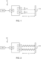
- As exemplified in
Figure 1 , anoptical proximity sensor 10 relying on direct time-of-flight techniques may comprise a timing andcontrol unit 100, anoptical transmitter 102, anoptical receiver 104 and optionally a human-machine interface 106. The timing andcontrol unit 100 generates a control signal for theoptical transmitter 102 which causes emission of an optical pulse from the optical transmitter, and at the same time tstart triggers a timer internal to the timing andcontrol unit 100. The optical pulse propagates towards atarget object 110 and some of the backscattered light travels back to theoptical receiver 104. An optical pulse being sensed at thereceiver 104 causes the internal timer to stop at a certain time tstop . In an exemplary implementation, the distance D between theoptical proximity sensor 10 and thetarget object 110 may be computed as D = c·Δt/2, where c is the propagation speed of light and Δt = tstop -tstart. - Mechanically scanning LIDAR devices (LIght Detection And Ranging) for use, e.g., in advanced driver assistance systems (ADAS) are exemplary of optical proximity sensors relying on direct time-of-flight techniques.
- It is noted that known sensors relying on time-domain reflectometry are not suitable to provide low cost rangefinders with good resolution over short distances since this may involve the use of expensive broadband electronics, e.g., because a time resolution of a few picoseconds (1 ps = 10-12 s) is involved for obtaining a distance resolution in the order of a millimeter (1 mm = 10-3 m). Also, known sensors relying on time-domain reflectometry may involve bulky and complex instrumentation, which may not be suitable for low cost applications.
- As exemplified in
Figure 2 , a knownoptical proximity sensor 20 relying on frequency-domain reflectometry may comprise a timing andcontrol unit 200, anoptical transmitter 202, anoptical receiver 204 and optionally a human-machine interface 206. The timing andcontrol unit 200 generates a control signal for theoptical emitter 202 which causes emission of an optical signal, whose intensity (amplitude) is modulated over time, from theoptical transmitter 202. The intensity of the emitted optical signal may be modulated periodically and expressed, for instance, as ITX(t) = I1(1+cos(ωmt+ΦTX)), where ωm is the modulation frequency (in rad/s) of the emitted optical signal and ΦTX is the phase of the emitted optical signal. The optical signal propagates towards atarget object 210 and a reflected optical signal having intensity IRX(t) = I2(1+cos(ωmt+ΦRX))+IBL travels back to theoptical receiver 204, where ωm is the modulation frequency (in rad/s) of the received optical signal (equal to the modulation frequency of the emitted optical signal), ΦRX is the phase of the received optical signal and IBL is the intensity of the environmental background light. The reflected optical signal (e.g., the envelope thereof) received at thereceiver 204 is compared to the emitted (reference) optical signal to determine a phase shift ΔΦ = ΦRX-ΦTX between the emitted and received optical signals. In an exemplary implementation, the distance D between theoptical proximity sensor 20 and thetarget object 210 may be computed as D = c·ΔΦ/ (2ωm), where c is again the propagation speed of light. - The known sensors relying on frequency-domain reflectometry are not suitable to provide low cost optical sensors insofar as they may involve complex systems, expensive electronics, accurate mechanical alignment between
light emitter 202 andlight detector 204, and temperature calibration. - Sensors relying on light intensity evaluation may be affected by different light intensity environmental conditions and may involve a calibration phase and/or the implementation of calibrated look-up tables.
- Document
US 2016/0320173 A1 discloses a method of measuring a change in an optical path length using differential laser self-mixing interferometry, and a corresponding measuring system. The method includes obtaining a reference self-mixing interferometric (SMI) signal and a main measurement SMI signal of a laser having a laser cavity, and determining the relative change in the optical path length between the laser and the target in a range between 0 and λ/2, by comparing the relative positions along time of fringes or transitions of the main and reference SMI signals. The reference SMI signal and the main SMI signal are obtained at different moments once backscattered laser light is generated from the reflection on the target of a reference and a main measurement laser light beam emitted by the laser and while being modulated according to a specific modulation pattern that is maintained while both the reference SMI signal and the main SMI signal are acquired and has re-entered its laser cavity. - The following documents are also exemplary of the prior art in the field of optical sensors: Karami et al., "Light emission enhancement in Light Emitting Single-Photon Avalanche Diodes (LESPADs)", Optik, Wissenschaftliche Verlag GmbH, vol. 126, no. 23, 12 August 2015, pages 4146-4148; Norgia et al., "High resolution self-mixing laser rangefinder", Review of Scientific Instruments, AIP, Melville, NY, US, vol. 83, no. 4, April 2012, pages 45113-45113; and
- Despite the extensive activity in the area, further improved solutions are desirable.
- For instance, low cost optical proximity sensors suitable for short-range distance measurements (e.g., with a range of approximately 0.5 m) are desirable.
- An object of one or more embodiments is to contribute in providing such improved solutions.
- According to one or more embodiments, such an object can be achieved by means of an optical proximity sensor having the features set forth in the claims that follow.
- One or more embodiments may relate to a corresponding method of operating the optical proximity sensor.
- The claims are an integral part of the technical teaching provided herein in respect of the embodiments.
- One or more embodiments provide an optical proximity sensor comprising at least one solid-state device acting both as light emitter and as light detector. The solid-state device comprises at least one of an array of single photon avalanche diodes (SPADs), an array of avalanche photodiodes (APDs), or a silicon photomultiplier (SiPM).
- According to the invention, the optical proximity sensor comprises a driver circuit configured for biasing said emitter/detector device with a (periodically) modulated signal to cause emission of a modulated optical signal (e.g., having an intensity which varies over time).
- In one or more embodiments, the driver circuit may be (fully) integrated within the optical proximity sensor to provide a so-called "single-chip" device. Alternatively, the driver circuit may be implemented on a different chip and coupled to the emitter/detector device.
- In one or more embodiments, the optical parts of the sensor (e.g., lenses and/or coatings and/or layers with optical properties) may be (fully) integrated within the optical proximity sensor, e.g., by process integration. Alternatively, the optical parts of the sensor may be discrete components.
- One or more embodiments may thus facilitate providing low cost optical proximity sensors for short-range measurements with improved accuracy.
- One or more embodiments will now be described, by way of example only, with reference to the annexed figures, wherein:
-
Figures 1 and 2 have already been described in the foregoing; -
Figures 3 to 8 are schematic block diagrams exemplary of optical proximity sensors according to various embodiments; and -
Figures 9 and 10 are exploded cross sections (side views) exemplary of implementation details of optical proximity sensors according to various embodiments. - In the ensuing description, one or more specific details are illustrated, aimed at providing an in-depth understanding of examples of embodiments of this description. The embodiments may be obtained without one or more of the specific details, or with other methods, components, materials, etc. In other cases, known structures, materials, or operations are not illustrated or described in detail so that certain aspects of embodiments will not be obscured.
- Reference to "an embodiment" or "one embodiment" in the framework of the present description is intended to indicate that a particular configuration, structure, or characteristic described in relation to the embodiment is comprised in at least one embodiment. Hence, phrases such as "in an embodiment" or "in one embodiment" that may be present in one or more points of the present description do not necessarily refer to one and the same embodiment. Moreover, particular conformations, structures, or characteristics may be combined in any adequate way in one or more embodiments.
- Throughout the figures annexed herein, like parts or elements are indicated with like references/numerals and a corresponding description will not be repeated for brevity.
- The references used herein are provided merely for convenience and hence do not define the extent of protection or the scope of the embodiments.
-
Figure 3 is a schematic block diagram exemplary of anoptical proximity sensor 30 according to one or more embodiments. Thesensor 30 comprises a solid-state device 300 configured to operate both as a light emitter and as a light detector (a photo-electric converter device). The emitter/detector device 300 comprises an array of single photon avalanche diodes (SPADs) or avalanche photodiodes (APDs), or a silicon photomultiplier (SiPM). By way of non-limiting example, the array may comprise between 100 and 10000 SPADs or APDs. - Additionally, the emitter/
detector device 300 may comprise optical components such as lenses, coatings and layers with peculiar optical properties, which will be further described in the following. - The
sensor 30 comprises adriver circuit 302 configured for driving the emitter/detector device 300. In particular, thedriver circuit 302 may comprise a modulation circuit configured for biasing the emitter/detector device 300 with a modulated signal, e.g., a periodic signal having a certain modulation frequency (for instance, in the range of 100 MHz to 3 GHz). Thedriver circuit 302 may be integrated on the same chip of the emitter/detector device 300, or may be implemented on a different chip and coupled to the emitter/detector device 300. - The
sensor 30 may comprise asignal conditioning circuit 304 configured for receiving an output signal indicative of light intensity from the emitter/detector device 300 and conditioning said output signal, e.g., for subsequent processing in a digital or analog processing circuit. For instance, thesignal conditioning circuit 304 may comprise an (analog) amplification stage, an analog-to-digital converter (ADC) and a logic interface to a processing circuit. Thesignal conditioning circuit 304 may be integrated on the same chip of the emitter/detector device 300, or may be implemented on a different chip and coupled to the emitter/detector device 300. - The
sensor 30 may comprise a timing andcontrol unit 306 configured for generating one or more control signal(s) for the operation of thedriver circuit 302, and/or for processing one or more conditioned signals received from thesignal conditioning circuit 304. The timing andcontrol unit 306 may thus be configured to control operation of thewhole sensor 30. For instance, the timing andcontrol unit 306 may comprise a microcontroller circuit (MCU). - Therefore, one or more embodiments may comprise a
device 300 configured to operate both as a light emitter and as a light detector, which may advantageously result in reduced cost and/or complexity of thesensor 30. - In particular, the emitter/
detector device 300 comprises an array of SPADs or APDs, or a SiPM, biased with a reverse-bias voltage (well) above the breakdown voltage, which is notionally employed as a photodetector device. - It is noted that, in such operating condition, each SPAD or APD in the
device 300 statistically stays in a "quiescent" state (i.e., it prevents a current from flowing therethrough) for a certain time interval, e.g., 1 ms (1 ms = 10-3 s). In fact, due to thermal noise in the emitter/detector device 300, the SPADs or APDs in the array may randomly generate avalanche events at a certain rate. - It is noted that an avalanche event taking place in a SPAD or APD may in turn result in emission of one or more photons from that SPAD or APD, i.e., an avalanche process in silicon may result in light emission. For instance, it is noted that during an avalanche process, about three photons may be emitted every 105 carriers generated in the SPAD or APD. Since a SiPM may be operated with a certain gain factor, e.g., about 5·106, approximately 150 photons may be emitted on average by each SPAD or APD during an avalanche process.
- Therefore, an array of SPADs or APDs, or a SiPM, which is biased with a reverse-bias voltage above the breakdown voltage emits light with a certain intensity which may be a function of the biasing condition, insofar as the array of SPADs or APDs, or the SiPM, may comprise a high number of individual cells (e.g., hundreds or thousands of SPADs or APDs) so that, statistically, avalanche events happen at a constant rate even in absence of illumination, due to thermal generation of charge carriers.
- Therefore, the light emitted from the array of SPADs or APDs, or the SiPM, due to thermal generation effects (which in turn may cause avalanche effects, which in turn may result in light emission) may be modulated over time (e.g., at a certain frequency) by modulating the biasing condition of the array of SPADs or APDs, or the SiPM.
- For instance, in one embodiment, the biasing voltage of the array of SPADs or APDs, or the SiPM, may be (e.g., periodically) switched between a first value higher than the breakdown voltage and a second value lower than the breakdown voltage. Since light emission from the array of SPADs or APDs takes place (only) when the biasing voltage is above the breakdown voltage, such a biasing modulation scheme may result in emission of a (e.g., periodically) modulated optical signal (a sort of ON/OFF modulation), with such emitted optical signal being received at the same array of SPADs or APDs, which may also operate as a light detector, after reflection at a target object.
- Alternatively, the biasing voltage of the array of SPADs or APDs, or the SiPM, may be modulated between two values which are both higher than the breakdown voltage, but different from each other, thereby resulting in modulation of the intensity of a continuous optical signal.
- In one or more embodiments, the distance D between the
optical proximity sensor 30 and a target object may be calculated as D = c·ΔΦ/ (2ωm) or D = c·ΔΦ/(2·2πfm) where ωm is the modulation frequency of the emitted optical signal (in rad/s), fm is the modulation frequency of the emitted optical signal (in Hz, ωm = 2πfm) and ΔΦ is the phase difference measured between the modulated optical signal emitted by the emitter/detector device 300 and the corresponding modulated optical signal received at the emitter/detector device 300 after reflection by the target object. Therefore, for a measurement system with a given phase accuracy (e.g., fixed by design), the modulation frequency may be selected to be as high as possible so as to result in better distance accuracy. - The modulation frequency fm may determine the ambiguity-free distance range L of the sensor, with L = c/2fm. For instance, a modulation frequency of 300 MHz may result in a range of the sensor of approximately 0.5 m, and a modulation frequency of 1 GHz may result in a range of the sensor of approximately 0.15 m. In one or more embodiments, the modulation frequency fm may be selected in the range of 100 MHz to 3 GHz. For instance, the modulation frequency fm may be selected as a trade-off between a target distance accuracy and a target distance range of the sensor.
- It is noted that APDs, SPADs and/or SiPMs may have good timing jitter performances (e.g., a few tens of picoseconds) which however may not be sufficient to provide distance accuracy at the millimeter scale for an
optical proximity sensor 30. - Distance accuracy may be computed as σ(d) = c·σ(t)/2, where σ(t) is the uncertainty of a single time measurement, with σ(t) = σ(ϕ)/2πfm (σ(ϕ) being the phase accuracy). In one or more embodiments, distance accuracy may be improved by increasing a number M of measurements, insofar as M measurements may be approximated as a collection of (e.g., independent and identically distributed) random variables. Therefore, time uncertainty may be reduced by a factor


-
Figure 3 is exemplary of an embodiment wherein the emitter/detector device 300, thedriver circuit 302, thesignal conditioning circuit 304 and the timing andcontrol unit 306 are implemented on different chips. - Alternatively, as exemplified in the schematic block diagram of
Figure 4 , the emitter/detector device 300 and thedriver circuit 302 may be implemented on thesame chip 34. - Alternatively, as exemplified in the schematic block diagram of
Figure 5 , the emitter/detector device 300 and thesignal conditioning circuit 304 may be implemented on thesame chip 35. - Alternatively, as exemplified in the schematic block diagram of
Figure 6 , the emitter/detector device 300, thedriver circuit 302 and thesignal conditioning circuit 304 may be implemented on thesame chip 36. - In one or more embodiments as exemplified in
Figure 7 , the emitter/detector device 300 may comprise a plurality of light emitters/detectors 3007, e.g., a plurality of arrays of APDs or SPADs or a plurality of SiPMs. Providing a plurality of light emitters/detectors 3007 may facilitate executing a plurality M of measurements at the same time. - Additionally or alternatively, in one or more embodiments as exemplified in
Figure 8 , the emitter/detector device 300 may comprise areference channel 3008. Such areference channel 3008 may be integrated (in a similar way as the plurality of arrays) in a single chip within themain device 30. For example, in some applications areference channel 3008 may be useful for evaluating background light. - In one or more embodiments, the emitter/
detector device 300 may be placed in a case to avoid background illumination. - As exemplified in the exploded side view of
Figure 9 , the emitter/detector device 300 may comprise the following components/layers, which may be, for instance, discrete components: - 900: substrate,
- 901: array of APDs or SPADs, or SiPM,
- 902: anti-reflection coating,
- 903: background light (attenuation) filter, and
- 904: lens system.
- Alternatively, as exemplified in the exploded side view of
Figure 10 , the optical components of the emitter/detector device 300 may be integrated by process integration. For instance, the emitter/detector device 300 may comprise asubstrate 1000, an array of APDs or SPADs, orSiPM 1001, and a respective array ofmicrolenses 1002 with integrated anti-reflection coating and background light (attenuation) filter. - In one or more embodiments, a metal layer (e.g., a tungsten layer) may be provided between adjacent APD or SPAD cells to avoid optical cross talk.
- Of course, it will be understood that the embodiments exemplified in
Figures 3 to 6 may be combined with any of the embodiments exemplified inFigure 7, Figure 8 and any ofFigures 9 and 10 . - One or more embodiments may thus provide one or more of the following advantages over the prior art:
- good resolution for low-cost and short distance range applications,
- compact and simplified system, due to the use of a device providing at the same time emission and detection of optical signals,
- no need of mechanical alignment between light emitter and detector,
- distance measurements independent from light intensity,
- no need of calibration with distance or look-up tables,
- no need of temperature calibration, insofar as the mechanical mismatch between emitter and detector is suppressed and the measurements are independent from light intensity, and thus independent from detector/emitter sensitivity.
- The extent of protection is defined by the annexed claims.
Claims (11)
- An optical proximity sensor (30) comprising a solid-state photo-electric converter (300), a biasing circuit (302) for biasing the solid-state photo-electric converter, and a drive circuit (306), wherein the solid-state photo-electric converter (300) comprises at least one of:an array of single photon avalanche diodes,an array of avalanche photodiodes, anda silicon photomultiplier,and wherein the drive circuit (306) is configured to:control the biasing circuit (302) to apply to the solid-state photo-electric converter (300) a bias signal modulated between a first value and a second value, the second value different from the first value, wherein said first value of the bias signal is higher than a breakdown voltage of the solid-state photo-electric converter (300), and wherein a modulated optical signal is emitted by the solid-state photo-electric converter (300) towards a target object,receive (304) an electrical output signal from the solid-state photo-electric converter (300), the electrical output signal being a function of a modulated optical signal received at the solid-state photo-electric converter (300) as a result of reflection of said emitted modulated optical signal at said target object,perform a phase comparison of said modulated bias signal applied to the photo-electric converter (300) against said electrical output signal received from the solid-state photo-electric converter (300) and produce, as a result of said phase comparison, a phase shift signal which is a function of the phase shift between said modulated optical signal emitted by the solid-state photo-electric converter (300) and the modulated optical signal received at the solid-state photo-electric converter (300), andcompute a distance between the optical proximity sensor (30) and said target object as a function of said phase shift signal.
- The optical proximity sensor (30) of claim 1, wherein the biasing circuit (302) comprises a modulation circuit configured to modulate periodically said bias signal between said first value and said second value at a frequency of 100 MHz to 3 GHz, wherein an optical signal periodically modulated at a frequency of 100 MHz to 3 GHz is emitted by the solid-state photo-electric converter (300).
- The optical proximity sensor (30) of claim 1 or claim 2, wherein said second value of the bias signal is lower than said breakdown voltage of the solid-state photo-electric converter (300).
- The optical proximity sensor (30) of claim 1 or claim 2, wherein said second value of the bias signal is higher than said breakdown voltage of the solid-state photo-electric converter (300).
- The optical proximity sensor (30) of any of the previous claims, comprising a conditioning circuit (304) configured for conditioning said electrical output signal from the solid-state photo-electric converter (300) and providing a conditioned electrical signal to the drive circuit (306).
- The optical proximity sensor (30) of claim 5, wherein at least two of the solid-state photo-electric converter (300), the biasing circuit (302) and the conditioning circuit (304) are implemented on a same semiconductor chip (34; 35; 36).
- The optical proximity sensor (30) of any of the previous claims, wherein the solid-state photo-electric converter (300) comprises:an anti-reflection coating (902),a background light attenuation filter (903), anda lens (904).
- The optical proximity sensor (30) of any of the previous claims, wherein the solid-state photo-electric converter (300) comprises a respective array of lenses (1002), the lenses in the array of lenses having an anti-reflection coating and a background light attenuation filter incorporated therein.
- The optical proximity sensor (30) of any of the previous claims, wherein the solid-state photo-electric converter (300) comprises a reference channel (3008) configured to evaluate a background light.
- The optical proximity sensor (30) of any of the previous claims, wherein the drive circuit (306) is configured to:perform a plurality of phase comparisons of said modulated bias signal applied to the photo-electric converter (300) against said electrical output signal received from the solid-state photo-electric converter (300) and produce a respective plurality of values of said phase shift signal, andcompute a distance between the optical proximity sensor (30) and said target object as a function of said plurality of values of said phase shift signal.
- A method of operating an optical proximity sensor (30) according to any of the previous claims, the method comprising:applying to the solid-state photo-electric converter (300) a bias signal modulated between a first value and a second value, the second value different from the first value, wherein said first value of the bias signal is higher than a breakdown voltage of the solid-state photo-electric converter (300), and wherein a modulated optical signal is emitted by the solid-state photo-electric converter (300) towards a target object,receiving (304) an electrical output signal from the solid-state photo-electric converter (300), the electrical output signal being a function of a modulated optical signal received at the solid-state photo-electric converter (300) as a result of reflection of said emitted modulated optical signal at said target object,performing a phase comparison of said modulated bias signal applied to the photo-electric converter (300) against said electrical output signal received from the solid-state photo-electric converter (300),producing, as a result of said phase comparison, a phase shift signal which is a function of the phase shift between the modulated optical signal emitted by the solid-state photo-electric converter (300) and the modulated optical signal received at the solid-state photo-electric converter (300), andcomputing a distance between the optical proximity sensor (30) and said target object as a function of said phase shift signal.
Applications Claiming Priority (1)
| Application Number | Priority Date | Filing Date | Title |
|---|---|---|---|
| IT102019000015761A IT201900015761A1 (en) | 2019-09-06 | 2019-09-06 | Optical proximity sensor and corresponding operating procedure |
Publications (2)
| Publication Number | Publication Date |
|---|---|
| EP3789793A1 EP3789793A1 (en) | 2021-03-10 |
| EP3789793B1 true EP3789793B1 (en) | 2023-07-19 |
Family
ID=69173244
Family Applications (1)
| Application Number | Title | Priority Date | Filing Date |
|---|---|---|---|
| EP20192064.2A Active EP3789793B1 (en) | 2019-09-06 | 2020-08-21 | An optical proximity sensor and corresponding method of operation |
Country Status (4)
| Country | Link |
|---|---|
| US (1) | US20210072386A1 (en) |
| EP (1) | EP3789793B1 (en) |
| CN (2) | CN212905460U (en) |
| IT (1) | IT201900015761A1 (en) |
Families Citing this family (1)
| Publication number | Priority date | Publication date | Assignee | Title |
|---|---|---|---|---|
| CA3099061A1 (en) * | 2019-11-15 | 2021-05-15 | Op-Hygiene Ip Gmbh | Fluid dispenser with wake up sensor |
Family Cites Families (4)
| Publication number | Priority date | Publication date | Assignee | Title |
|---|---|---|---|---|
| US20050035361A1 (en) * | 2003-08-15 | 2005-02-17 | Peterson Charles M. | Polarized light emitting devices and methods |
| US7283214B2 (en) * | 2005-10-14 | 2007-10-16 | Microsoft Corporation | Self-mixing laser range sensor |
| EP2887008A1 (en) * | 2013-12-17 | 2015-06-24 | Universitat Politècnica de Catalunya | A method of measuring a change in an optical path using differential laser self-mixing interferometry and a differential laser self-mixing interferometry measuring system |
| TW202043800A (en) * | 2019-01-30 | 2020-12-01 | 日商索尼半導體解決方案公司 | Light receiving device and ranging system |
-
2019
- 2019-09-06 IT IT102019000015761A patent/IT201900015761A1/en unknown
-
2020
- 2020-08-21 EP EP20192064.2A patent/EP3789793B1/en active Active
- 2020-09-03 US US17/011,867 patent/US20210072386A1/en active Pending
- 2020-09-07 CN CN202021927590.XU patent/CN212905460U/en active Active
- 2020-09-07 CN CN202010927579.1A patent/CN112558093A/en active Pending
Also Published As
| Publication number | Publication date |
|---|---|
| IT201900015761A1 (en) | 2021-03-06 |
| CN212905460U (en) | 2021-04-06 |
| US20210072386A1 (en) | 2021-03-11 |
| CN112558093A (en) | 2021-03-26 |
| EP3789793A1 (en) | 2021-03-10 |
Similar Documents
| Publication | Publication Date | Title |
|---|---|---|
| US11022680B2 (en) | Distance measuring device with SPAD array and range walk compensenation | |
| CN110244311B (en) | Laser radar receiving device, laser radar system and laser ranging method | |
| CN211014629U (en) | Laser radar device | |
| US20180210084A1 (en) | Optoelectronic sensor and method of determining the distance of an object in a monitored zone | |
| US11725935B2 (en) | Distance meter comprising SPAD arrangement for consideration of multiple targets | |
| CN111868556A (en) | Method and system for high resolution remote flash LIDAR | |
| US11592292B2 (en) | Total station or theodolite having scanning functionality and settable receiving ranges of the receiver | |
| CN102692622B (en) | Laser detection method based on dense pulses | |
| US20240061091A1 (en) | Method for measuring reflectivity of target object by using lidar, and lidar | |
| US20200370955A1 (en) | Array of single-photon avalanche diode (spad) microcells and operating the same | |
| JP2009524072A (en) | Measuring method of light propagation time | |
| KR20190002013U (en) | LiDAR device | |
| JP2019090793A (en) | Range-finding type photoelectric sensor and range-finding method | |
| WO2023103310A1 (en) | Laser radar, and method and system thereof for measuring reflectivity of target | |
| EP3789793B1 (en) | An optical proximity sensor and corresponding method of operation | |
| CN108732578A (en) | Range-finding system and it is calibrated and is determined external object distance method | |
| US20220171038A1 (en) | Multichannel time-of-flight measurement device with time-to-digital converters in a programmable integrated circuit | |
| IL275400B1 (en) | Receiving arrangement for receiving light signals | |
| CA3085648C (en) | Arrangement and method for determining a distance of at least one object using light signals | |
| US20220155442A1 (en) | Light detection device, lidar device including the same, and method of measuring distance | |
| KR20220008734A (en) | Readout architecture for fmcw lidar | |
| Golovkov et al. | Receiving system of a pulsed laser rangefinder | |
| US20220244385A1 (en) | Lidar device and method of operating the same | |
| US20220075036A1 (en) | Range estimation for lidar systems using a detector array | |
| KR20220106646A (en) | Adaptive pulse shaper for direct time-of-flight depth sensors |
Legal Events
| Date | Code | Title | Description |
|---|---|---|---|
| PUAI | Public reference made under article 153(3) epc to a published international application that has entered the european phase |
Free format text: ORIGINAL CODE: 0009012 |
|
| STAA | Information on the status of an ep patent application or granted ep patent |
Free format text: STATUS: THE APPLICATION HAS BEEN PUBLISHED |
|
| AK | Designated contracting states |
Kind code of ref document: A1 Designated state(s): AL AT BE BG CH CY CZ DE DK EE ES FI FR GB GR HR HU IE IS IT LI LT LU LV MC MK MT NL NO PL PT RO RS SE SI SK SM TR |
|
| AX | Request for extension of the european patent |
Extension state: BA ME |
|
| STAA | Information on the status of an ep patent application or granted ep patent |
Free format text: STATUS: REQUEST FOR EXAMINATION WAS MADE |
|
| 17P | Request for examination filed |
Effective date: 20210803 |
|
| RBV | Designated contracting states (corrected) |
Designated state(s): AL AT BE BG CH CY CZ DE DK EE ES FI FR GB GR HR HU IE IS IT LI LT LU LV MC MK MT NL NO PL PT RO RS SE SI SK SM TR |
|
| GRAP | Despatch of communication of intention to grant a patent |
Free format text: ORIGINAL CODE: EPIDOSNIGR1 |
|
| STAA | Information on the status of an ep patent application or granted ep patent |
Free format text: STATUS: GRANT OF PATENT IS INTENDED |
|
| INTG | Intention to grant announced |
Effective date: 20230322 |
|
| GRAS | Grant fee paid |
Free format text: ORIGINAL CODE: EPIDOSNIGR3 |
|
| GRAA | (expected) grant |
Free format text: ORIGINAL CODE: 0009210 |
|
| STAA | Information on the status of an ep patent application or granted ep patent |
Free format text: STATUS: THE PATENT HAS BEEN GRANTED |
|
| AK | Designated contracting states |
Kind code of ref document: B1 Designated state(s): AL AT BE BG CH CY CZ DE DK EE ES FI FR GB GR HR HU IE IS IT LI LT LU LV MC MK MT NL NO PL PT RO RS SE SI SK SM TR |
|
| REG | Reference to a national code |
Ref country code: GB Ref legal event code: FG4D |
|
| REG | Reference to a national code |
Ref country code: CH Ref legal event code: EP |
|
| REG | Reference to a national code |
Ref country code: DE Ref legal event code: R096 Ref document number: 602020013967 Country of ref document: DE |
|
| REG | Reference to a national code |
Ref country code: IE Ref legal event code: FG4D |
|
| REG | Reference to a national code |
Ref country code: LT Ref legal event code: MG9D |
|
| REG | Reference to a national code |
Ref country code: NL Ref legal event code: MP Effective date: 20230719 |
|
| PGFP | Annual fee paid to national office [announced via postgrant information from national office to epo] |
Ref country code: DE Payment date: 20230720 Year of fee payment: 4 |
|
| REG | Reference to a national code |
Ref country code: AT Ref legal event code: MK05 Ref document number: 1590003 Country of ref document: AT Kind code of ref document: T Effective date: 20230719 |
|
| PG25 | Lapsed in a contracting state [announced via postgrant information from national office to epo] |
Ref country code: NL Free format text: LAPSE BECAUSE OF FAILURE TO SUBMIT A TRANSLATION OF THE DESCRIPTION OR TO PAY THE FEE WITHIN THE PRESCRIBED TIME-LIMIT Effective date: 20230719 |
|
| PG25 | Lapsed in a contracting state [announced via postgrant information from national office to epo] |
Ref country code: GR Free format text: LAPSE BECAUSE OF FAILURE TO SUBMIT A TRANSLATION OF THE DESCRIPTION OR TO PAY THE FEE WITHIN THE PRESCRIBED TIME-LIMIT Effective date: 20231020 |
|
| PG25 | Lapsed in a contracting state [announced via postgrant information from national office to epo] |
Ref country code: IS Free format text: LAPSE BECAUSE OF FAILURE TO SUBMIT A TRANSLATION OF THE DESCRIPTION OR TO PAY THE FEE WITHIN THE PRESCRIBED TIME-LIMIT Effective date: 20231119 |
|
| PG25 | Lapsed in a contracting state [announced via postgrant information from national office to epo] |
Ref country code: SE Free format text: LAPSE BECAUSE OF FAILURE TO SUBMIT A TRANSLATION OF THE DESCRIPTION OR TO PAY THE FEE WITHIN THE PRESCRIBED TIME-LIMIT Effective date: 20230719 Ref country code: RS Free format text: LAPSE BECAUSE OF FAILURE TO SUBMIT A TRANSLATION OF THE DESCRIPTION OR TO PAY THE FEE WITHIN THE PRESCRIBED TIME-LIMIT Effective date: 20230719 Ref country code: PT Free format text: LAPSE BECAUSE OF FAILURE TO SUBMIT A TRANSLATION OF THE DESCRIPTION OR TO PAY THE FEE WITHIN THE PRESCRIBED TIME-LIMIT Effective date: 20231120 Ref country code: NO Free format text: LAPSE BECAUSE OF FAILURE TO SUBMIT A TRANSLATION OF THE DESCRIPTION OR TO PAY THE FEE WITHIN THE PRESCRIBED TIME-LIMIT Effective date: 20231019 Ref country code: LV Free format text: LAPSE BECAUSE OF FAILURE TO SUBMIT A TRANSLATION OF THE DESCRIPTION OR TO PAY THE FEE WITHIN THE PRESCRIBED TIME-LIMIT Effective date: 20230719 Ref country code: LT Free format text: LAPSE BECAUSE OF FAILURE TO SUBMIT A TRANSLATION OF THE DESCRIPTION OR TO PAY THE FEE WITHIN THE PRESCRIBED TIME-LIMIT Effective date: 20230719 Ref country code: IS Free format text: LAPSE BECAUSE OF FAILURE TO SUBMIT A TRANSLATION OF THE DESCRIPTION OR TO PAY THE FEE WITHIN THE PRESCRIBED TIME-LIMIT Effective date: 20231119 Ref country code: HR Free format text: LAPSE BECAUSE OF FAILURE TO SUBMIT A TRANSLATION OF THE DESCRIPTION OR TO PAY THE FEE WITHIN THE PRESCRIBED TIME-LIMIT Effective date: 20230719 Ref country code: GR Free format text: LAPSE BECAUSE OF FAILURE TO SUBMIT A TRANSLATION OF THE DESCRIPTION OR TO PAY THE FEE WITHIN THE PRESCRIBED TIME-LIMIT Effective date: 20231020 Ref country code: FI Free format text: LAPSE BECAUSE OF FAILURE TO SUBMIT A TRANSLATION OF THE DESCRIPTION OR TO PAY THE FEE WITHIN THE PRESCRIBED TIME-LIMIT Effective date: 20230719 Ref country code: AT Free format text: LAPSE BECAUSE OF FAILURE TO SUBMIT A TRANSLATION OF THE DESCRIPTION OR TO PAY THE FEE WITHIN THE PRESCRIBED TIME-LIMIT Effective date: 20230719 |
|
| PG25 | Lapsed in a contracting state [announced via postgrant information from national office to epo] |
Ref country code: PL Free format text: LAPSE BECAUSE OF FAILURE TO SUBMIT A TRANSLATION OF THE DESCRIPTION OR TO PAY THE FEE WITHIN THE PRESCRIBED TIME-LIMIT Effective date: 20230719 |
|
| REG | Reference to a national code |
Ref country code: CH Ref legal event code: PL |
|
| PG25 | Lapsed in a contracting state [announced via postgrant information from national office to epo] |
Ref country code: LU Free format text: LAPSE BECAUSE OF NON-PAYMENT OF DUE FEES Effective date: 20230821 |
|
| PG25 | Lapsed in a contracting state [announced via postgrant information from national office to epo] |
Ref country code: ES Free format text: LAPSE BECAUSE OF FAILURE TO SUBMIT A TRANSLATION OF THE DESCRIPTION OR TO PAY THE FEE WITHIN THE PRESCRIBED TIME-LIMIT Effective date: 20230719 |
|
| PG25 | Lapsed in a contracting state [announced via postgrant information from national office to epo] |
Ref country code: SM Free format text: LAPSE BECAUSE OF FAILURE TO SUBMIT A TRANSLATION OF THE DESCRIPTION OR TO PAY THE FEE WITHIN THE PRESCRIBED TIME-LIMIT Effective date: 20230719 Ref country code: RO Free format text: LAPSE BECAUSE OF FAILURE TO SUBMIT A TRANSLATION OF THE DESCRIPTION OR TO PAY THE FEE WITHIN THE PRESCRIBED TIME-LIMIT Effective date: 20230719 Ref country code: LU Free format text: LAPSE BECAUSE OF NON-PAYMENT OF DUE FEES Effective date: 20230821 Ref country code: ES Free format text: LAPSE BECAUSE OF FAILURE TO SUBMIT A TRANSLATION OF THE DESCRIPTION OR TO PAY THE FEE WITHIN THE PRESCRIBED TIME-LIMIT Effective date: 20230719 Ref country code: EE Free format text: LAPSE BECAUSE OF FAILURE TO SUBMIT A TRANSLATION OF THE DESCRIPTION OR TO PAY THE FEE WITHIN THE PRESCRIBED TIME-LIMIT Effective date: 20230719 Ref country code: DK Free format text: LAPSE BECAUSE OF FAILURE TO SUBMIT A TRANSLATION OF THE DESCRIPTION OR TO PAY THE FEE WITHIN THE PRESCRIBED TIME-LIMIT Effective date: 20230719 Ref country code: CZ Free format text: LAPSE BECAUSE OF FAILURE TO SUBMIT A TRANSLATION OF THE DESCRIPTION OR TO PAY THE FEE WITHIN THE PRESCRIBED TIME-LIMIT Effective date: 20230719 Ref country code: SK Free format text: LAPSE BECAUSE OF FAILURE TO SUBMIT A TRANSLATION OF THE DESCRIPTION OR TO PAY THE FEE WITHIN THE PRESCRIBED TIME-LIMIT Effective date: 20230719 Ref country code: MC Free format text: LAPSE BECAUSE OF FAILURE TO SUBMIT A TRANSLATION OF THE DESCRIPTION OR TO PAY THE FEE WITHIN THE PRESCRIBED TIME-LIMIT Effective date: 20230719 Ref country code: CH Free format text: LAPSE BECAUSE OF NON-PAYMENT OF DUE FEES Effective date: 20230831 |