EP3789464A1 - Ink composition for organic light emitting device - Google Patents
Ink composition for organic light emitting device Download PDFInfo
- Publication number
- EP3789464A1 EP3789464A1 EP19866928.5A EP19866928A EP3789464A1 EP 3789464 A1 EP3789464 A1 EP 3789464A1 EP 19866928 A EP19866928 A EP 19866928A EP 3789464 A1 EP3789464 A1 EP 3789464A1
- Authority
- EP
- European Patent Office
- Prior art keywords
- com
- group
- solvent
- substituted
- unsubstituted
- Prior art date
- Legal status (The legal status is an assumption and is not a legal conclusion. Google has not performed a legal analysis and makes no representation as to the accuracy of the status listed.)
- Granted
Links
- 0 *C(C(CC1)=CC2=C1c1ccccc1C2(c1ccccc1)c(cc1)ccc1C#Cc1ccc(C=C)cc1)c(cc1)ccc1-c1ccccc1 Chemical compound *C(C(CC1)=CC2=C1c1ccccc1C2(c1ccccc1)c(cc1)ccc1C#Cc1ccc(C=C)cc1)c(cc1)ccc1-c1ccccc1 0.000 description 23
- UDLXAAWWGCIXRX-UHFFFAOYSA-N C=CCOc1ccc(C2(c(cc(cc3)N(c4ccccc4)c(cc4)ccc4-c(cc4)ccc4N(c4ccccc4)c(cc4)cc5c4-c4ccccc4C5(c(cc4)ccc4OCC=C)c(cc4)ccc4F)c3-c3ccccc23)c(cc2)ccc2F)cc1 Chemical compound C=CCOc1ccc(C2(c(cc(cc3)N(c4ccccc4)c(cc4)ccc4-c(cc4)ccc4N(c4ccccc4)c(cc4)cc5c4-c4ccccc4C5(c(cc4)ccc4OCC=C)c(cc4)ccc4F)c3-c3ccccc23)c(cc2)ccc2F)cc1 UDLXAAWWGCIXRX-UHFFFAOYSA-N 0.000 description 1
- XSXRZSFEFKBLMY-UHFFFAOYSA-N C=Cc(cc1)ccc1Oc1ccc(C2(c3cc(N(c4ccccc4)c(cc4)ccc4-c(cc4)ccc4N(c4ccccc4)c(cc4)cc5c4-c4ccccc4C5(c(cc4)ccc4Oc4ccc(C=C)cc4)c(cc4)ccc4F)ccc3-c3c2cccc3)c(cc2)ccc2F)cc1 Chemical compound C=Cc(cc1)ccc1Oc1ccc(C2(c3cc(N(c4ccccc4)c(cc4)ccc4-c(cc4)ccc4N(c4ccccc4)c(cc4)cc5c4-c4ccccc4C5(c(cc4)ccc4Oc4ccc(C=C)cc4)c(cc4)ccc4F)ccc3-c3c2cccc3)c(cc2)ccc2F)cc1 XSXRZSFEFKBLMY-UHFFFAOYSA-N 0.000 description 1
- LDCYPUJYPMFXEL-UHFFFAOYSA-N C=Cc1ccc(CC2(c3cc(N(c4ccccc4)c(cc4)ccc4-c(cc4)ccc4N(c4ccccc4)c(cc45)ccc4-c4ccccc4C5(Cc4ccc(C=C)cc4)c4ccc(C(F)(F)F)cc4)ccc3-c3c2cccc3)c2ccc(C(F)(F)F)cc2)cc1 Chemical compound C=Cc1ccc(CC2(c3cc(N(c4ccccc4)c(cc4)ccc4-c(cc4)ccc4N(c4ccccc4)c(cc45)ccc4-c4ccccc4C5(Cc4ccc(C=C)cc4)c4ccc(C(F)(F)F)cc4)ccc3-c3c2cccc3)c2ccc(C(F)(F)F)cc2)cc1 LDCYPUJYPMFXEL-UHFFFAOYSA-N 0.000 description 1
- FEYNTCCNCIFFOJ-UHFFFAOYSA-N C=Cc1ccc(COc2ccc(C3(c4cc(N(c5ccccc5)c(cc5)ccc5-c(cc5)ccc5N(c5ccccc5)c(cc5)cc6c5-c5ccccc5C6(c(cc5)ccc5OCc5ccc(C=C)cc5)c(cc5)ccc5F)ccc4-c4c3cccc4)c(cc3)ccc3F)cc2)cc1 Chemical compound C=Cc1ccc(COc2ccc(C3(c4cc(N(c5ccccc5)c(cc5)ccc5-c(cc5)ccc5N(c5ccccc5)c(cc5)cc6c5-c5ccccc5C6(c(cc5)ccc5OCc5ccc(C=C)cc5)c(cc5)ccc5F)ccc4-c4c3cccc4)c(cc3)ccc3F)cc2)cc1 FEYNTCCNCIFFOJ-UHFFFAOYSA-N 0.000 description 1
- ZRSVUHYIDLPEIZ-UHFFFAOYSA-N CCC1(COc2ccc(C3(c(cc(cc4)N(c5ccccc5)c(cc5)ccc5-c(cc5)ccc5N(c5ccccc5)c(cc5)cc(C6(c(cc7)ccc7SCC7(CC)COC7)c(cc7)ccc7SCC7(CC)COC7)c5-c5c6cccc5)c4-c4ccccc34)c3ccccc3)cc2)COC1 Chemical compound CCC1(COc2ccc(C3(c(cc(cc4)N(c5ccccc5)c(cc5)ccc5-c(cc5)ccc5N(c5ccccc5)c(cc5)cc(C6(c(cc7)ccc7SCC7(CC)COC7)c(cc7)ccc7SCC7(CC)COC7)c5-c5c6cccc5)c4-c4ccccc34)c3ccccc3)cc2)COC1 ZRSVUHYIDLPEIZ-UHFFFAOYSA-N 0.000 description 1
- FXKXWIVRYXWXDH-UHFFFAOYSA-N CCC1(COc2ccc(C3(c4cc(N(c5ccccc5)c(cc5)ccc5-c(cc5)ccc5N(c5ccccc5)c(cc5)cc6c5-c5ccccc5C6(c(cc5)ccc5SCC5(CC)COC5)c(cc5)ccc5SCC5(CC)COC5)ccc4-c4c3cccc4)c(cc3)ccc3OCC3(CC)COC3)cc2)COC1 Chemical compound CCC1(COc2ccc(C3(c4cc(N(c5ccccc5)c(cc5)ccc5-c(cc5)ccc5N(c5ccccc5)c(cc5)cc6c5-c5ccccc5C6(c(cc5)ccc5SCC5(CC)COC5)c(cc5)ccc5SCC5(CC)COC5)ccc4-c4c3cccc4)c(cc3)ccc3OCC3(CC)COC3)cc2)COC1 FXKXWIVRYXWXDH-UHFFFAOYSA-N 0.000 description 1
- DZXHSENITGPKBJ-UHFFFAOYSA-N CCC1(CSc2ccc(C3(c(cc(cc4)N(c5ccccc5)c(cc5)ccc5-c(cc5)ccc5N(c5ccccc5)c(cc5)cc6c5-c5ccccc5C6(c(cc5)ccc5Oc5ccccc5)c(cc5)ccc5SCC5(CC)COC5)c4-c4ccccc34)c(cc3)ccc3Oc3ccccc3)cc2)COC1 Chemical compound CCC1(CSc2ccc(C3(c(cc(cc4)N(c5ccccc5)c(cc5)ccc5-c(cc5)ccc5N(c5ccccc5)c(cc5)cc6c5-c5ccccc5C6(c(cc5)ccc5Oc5ccccc5)c(cc5)ccc5SCC5(CC)COC5)c4-c4ccccc34)c(cc3)ccc3Oc3ccccc3)cc2)COC1 DZXHSENITGPKBJ-UHFFFAOYSA-N 0.000 description 1
- NYVKPOJKEHKHHA-UHFFFAOYSA-N CCC1(CSc2ccc(C3(c4cc(N(c5ccccc5)c(cc5)ccc5-c(cc5)ccc5N(c5ccccc5)c(cc5)cc6c5-c5ccccc5C6(c(cc5)ccc5F)c(cc5)ccc5SCC5(CC)COC5)ccc4-c4c3cccc4)c(cc3)ccc3F)cc2)COC1 Chemical compound CCC1(CSc2ccc(C3(c4cc(N(c5ccccc5)c(cc5)ccc5-c(cc5)ccc5N(c5ccccc5)c(cc5)cc6c5-c5ccccc5C6(c(cc5)ccc5F)c(cc5)ccc5SCC5(CC)COC5)ccc4-c4c3cccc4)c(cc3)ccc3F)cc2)COC1 NYVKPOJKEHKHHA-UHFFFAOYSA-N 0.000 description 1
- SKWKVHILQXLWNM-UHFFFAOYSA-N CCC1(CSc2ccc(C3(c4cc(N(c5ccccc5)c(cc5)ccc5-c(cc5)ccc5N(c5ccccc5)c(cc5)cc6c5-c5ccccc5C6(c(cc5)ccc5SCC5(CC)COC5)c5cc(cccc6)c6cc5)ccc4-c4c3cccc4)c3cc4ccccc4cc3)cc2)COC1 Chemical compound CCC1(CSc2ccc(C3(c4cc(N(c5ccccc5)c(cc5)ccc5-c(cc5)ccc5N(c5ccccc5)c(cc5)cc6c5-c5ccccc5C6(c(cc5)ccc5SCC5(CC)COC5)c5cc(cccc6)c6cc5)ccc4-c4c3cccc4)c3cc4ccccc4cc3)cc2)COC1 SKWKVHILQXLWNM-UHFFFAOYSA-N 0.000 description 1
- WJGGDVRIEHIVPU-UHFFFAOYSA-N CCOCCOc1ccc(C2(c(cc(cc3)N(c4ccccc4)c(cc4)ccc4-c(cc4)ccc4N(c4ccccc4)c(cc4)cc5c4-c4ccccc4C5(c(cc4)ccc4OCCOCC)c(cc4)ccc4SCC=C)c3-c3ccccc23)c(cc2)ccc2SCC=C)cc1 Chemical compound CCOCCOc1ccc(C2(c(cc(cc3)N(c4ccccc4)c(cc4)ccc4-c(cc4)ccc4N(c4ccccc4)c(cc4)cc5c4-c4ccccc4C5(c(cc4)ccc4OCCOCC)c(cc4)ccc4SCC=C)c3-c3ccccc23)c(cc2)ccc2SCC=C)cc1 WJGGDVRIEHIVPU-UHFFFAOYSA-N 0.000 description 1
- YCPRINAXORUHNI-UHFFFAOYSA-N CCOCCOc1ccc(C2(c3cc(N(c4ccccc4)c(cc4)ccc4-c(cc4)ccc4N(c4ccccc4)c(cc4)cc5c4-c4ccccc4C5(c(cc4)ccc4OCCOCC)c(cc4)ccc4SCc4ccc(C=C)cc4)ccc3-c3c2cccc3)c(cc2)ccc2SCc2ccc(C=C)cc2)cc1 Chemical compound CCOCCOc1ccc(C2(c3cc(N(c4ccccc4)c(cc4)ccc4-c(cc4)ccc4N(c4ccccc4)c(cc4)cc5c4-c4ccccc4C5(c(cc4)ccc4OCCOCC)c(cc4)ccc4SCc4ccc(C=C)cc4)ccc3-c3c2cccc3)c(cc2)ccc2SCc2ccc(C=C)cc2)cc1 YCPRINAXORUHNI-UHFFFAOYSA-N 0.000 description 1
- IIHIJFJSXPDTNO-UHFFFAOYSA-N COC(C1CCCC1)=O Chemical compound COC(C1CCCC1)=O IIHIJFJSXPDTNO-UHFFFAOYSA-N 0.000 description 1
- ZUNSDEVCBWMHMO-UHFFFAOYSA-N COC(F)=C(F)F Chemical compound COC(F)=C(F)F ZUNSDEVCBWMHMO-UHFFFAOYSA-N 0.000 description 1
- QPJVMBTYPHYUOC-UHFFFAOYSA-N COC(c1ccccc1)=O Chemical compound COC(c1ccccc1)=O QPJVMBTYPHYUOC-UHFFFAOYSA-N 0.000 description 1
- IHOIVNLJXBZYSK-UHFFFAOYSA-N COc1ccc(C2(c3cc(N(c4ccccc4)c(cc4)ccc4-c(cc4)ccc4N(c4ccccc4)c(cc4)cc5c4-c4ccccc4C5(c(cc4)ccc4OC)c(cc4)ccc4SCC=C)ccc3-c3c2cccc3)c(cc2)ccc2SCC=C)cc1 Chemical compound COc1ccc(C2(c3cc(N(c4ccccc4)c(cc4)ccc4-c(cc4)ccc4N(c4ccccc4)c(cc4)cc5c4-c4ccccc4C5(c(cc4)ccc4OC)c(cc4)ccc4SCC=C)ccc3-c3c2cccc3)c(cc2)ccc2SCC=C)cc1 IHOIVNLJXBZYSK-UHFFFAOYSA-N 0.000 description 1
- QUIDNHBHDCKTJC-UHFFFAOYSA-N Fc1ccc(C2(c(cc(cc3)N(c4ccccc4)c(cc4)ccc4-c(cc4)ccc4N(c4ccccc4)c(cc4C5(c(cc6)ccc6Oc6ccc(CC7)c7c6)c(cc6)ccc6F)ccc4-c4c5cccc4)c3-c3ccccc23)c(cc2)ccc2Oc2cc(CC3)c3cc2)cc1 Chemical compound Fc1ccc(C2(c(cc(cc3)N(c4ccccc4)c(cc4)ccc4-c(cc4)ccc4N(c4ccccc4)c(cc4C5(c(cc6)ccc6Oc6ccc(CC7)c7c6)c(cc6)ccc6F)ccc4-c4c5cccc4)c3-c3ccccc23)c(cc2)ccc2Oc2cc(CC3)c3cc2)cc1 QUIDNHBHDCKTJC-UHFFFAOYSA-N 0.000 description 1
Images

Classifications
-
- C—CHEMISTRY; METALLURGY
- C09—DYES; PAINTS; POLISHES; NATURAL RESINS; ADHESIVES; COMPOSITIONS NOT OTHERWISE PROVIDED FOR; APPLICATIONS OF MATERIALS NOT OTHERWISE PROVIDED FOR
- C09D—COATING COMPOSITIONS, e.g. PAINTS, VARNISHES OR LACQUERS; FILLING PASTES; CHEMICAL PAINT OR INK REMOVERS; INKS; CORRECTING FLUIDS; WOODSTAINS; PASTES OR SOLIDS FOR COLOURING OR PRINTING; USE OF MATERIALS THEREFOR
- C09D11/00—Inks
- C09D11/50—Sympathetic, colour changing or similar inks
-
- C—CHEMISTRY; METALLURGY
- C09—DYES; PAINTS; POLISHES; NATURAL RESINS; ADHESIVES; COMPOSITIONS NOT OTHERWISE PROVIDED FOR; APPLICATIONS OF MATERIALS NOT OTHERWISE PROVIDED FOR
- C09D—COATING COMPOSITIONS, e.g. PAINTS, VARNISHES OR LACQUERS; FILLING PASTES; CHEMICAL PAINT OR INK REMOVERS; INKS; CORRECTING FLUIDS; WOODSTAINS; PASTES OR SOLIDS FOR COLOURING OR PRINTING; USE OF MATERIALS THEREFOR
- C09D11/00—Inks
- C09D11/02—Printing inks
- C09D11/03—Printing inks characterised by features other than the chemical nature of the binder
- C09D11/033—Printing inks characterised by features other than the chemical nature of the binder characterised by the solvent
-
- C—CHEMISTRY; METALLURGY
- C09—DYES; PAINTS; POLISHES; NATURAL RESINS; ADHESIVES; COMPOSITIONS NOT OTHERWISE PROVIDED FOR; APPLICATIONS OF MATERIALS NOT OTHERWISE PROVIDED FOR
- C09D—COATING COMPOSITIONS, e.g. PAINTS, VARNISHES OR LACQUERS; FILLING PASTES; CHEMICAL PAINT OR INK REMOVERS; INKS; CORRECTING FLUIDS; WOODSTAINS; PASTES OR SOLIDS FOR COLOURING OR PRINTING; USE OF MATERIALS THEREFOR
- C09D11/00—Inks
- C09D11/02—Printing inks
- C09D11/03—Printing inks characterised by features other than the chemical nature of the binder
- C09D11/037—Printing inks characterised by features other than the chemical nature of the binder characterised by the pigment
-
- C—CHEMISTRY; METALLURGY
- C09—DYES; PAINTS; POLISHES; NATURAL RESINS; ADHESIVES; COMPOSITIONS NOT OTHERWISE PROVIDED FOR; APPLICATIONS OF MATERIALS NOT OTHERWISE PROVIDED FOR
- C09D—COATING COMPOSITIONS, e.g. PAINTS, VARNISHES OR LACQUERS; FILLING PASTES; CHEMICAL PAINT OR INK REMOVERS; INKS; CORRECTING FLUIDS; WOODSTAINS; PASTES OR SOLIDS FOR COLOURING OR PRINTING; USE OF MATERIALS THEREFOR
- C09D11/00—Inks
- C09D11/30—Inkjet printing inks
- C09D11/32—Inkjet printing inks characterised by colouring agents
- C09D11/322—Pigment inks
-
- C—CHEMISTRY; METALLURGY
- C09—DYES; PAINTS; POLISHES; NATURAL RESINS; ADHESIVES; COMPOSITIONS NOT OTHERWISE PROVIDED FOR; APPLICATIONS OF MATERIALS NOT OTHERWISE PROVIDED FOR
- C09D—COATING COMPOSITIONS, e.g. PAINTS, VARNISHES OR LACQUERS; FILLING PASTES; CHEMICAL PAINT OR INK REMOVERS; INKS; CORRECTING FLUIDS; WOODSTAINS; PASTES OR SOLIDS FOR COLOURING OR PRINTING; USE OF MATERIALS THEREFOR
- C09D11/00—Inks
- C09D11/30—Inkjet printing inks
- C09D11/32—Inkjet printing inks characterised by colouring agents
- C09D11/328—Inkjet printing inks characterised by colouring agents characterised by dyes
-
- C—CHEMISTRY; METALLURGY
- C09—DYES; PAINTS; POLISHES; NATURAL RESINS; ADHESIVES; COMPOSITIONS NOT OTHERWISE PROVIDED FOR; APPLICATIONS OF MATERIALS NOT OTHERWISE PROVIDED FOR
- C09D—COATING COMPOSITIONS, e.g. PAINTS, VARNISHES OR LACQUERS; FILLING PASTES; CHEMICAL PAINT OR INK REMOVERS; INKS; CORRECTING FLUIDS; WOODSTAINS; PASTES OR SOLIDS FOR COLOURING OR PRINTING; USE OF MATERIALS THEREFOR
- C09D11/00—Inks
- C09D11/30—Inkjet printing inks
- C09D11/36—Inkjet printing inks based on non-aqueous solvents
-
- C—CHEMISTRY; METALLURGY
- C09—DYES; PAINTS; POLISHES; NATURAL RESINS; ADHESIVES; COMPOSITIONS NOT OTHERWISE PROVIDED FOR; APPLICATIONS OF MATERIALS NOT OTHERWISE PROVIDED FOR
- C09D—COATING COMPOSITIONS, e.g. PAINTS, VARNISHES OR LACQUERS; FILLING PASTES; CHEMICAL PAINT OR INK REMOVERS; INKS; CORRECTING FLUIDS; WOODSTAINS; PASTES OR SOLIDS FOR COLOURING OR PRINTING; USE OF MATERIALS THEREFOR
- C09D11/00—Inks
- C09D11/30—Inkjet printing inks
- C09D11/38—Inkjet printing inks characterised by non-macromolecular additives other than solvents, pigments or dyes
-
- C—CHEMISTRY; METALLURGY
- C09—DYES; PAINTS; POLISHES; NATURAL RESINS; ADHESIVES; COMPOSITIONS NOT OTHERWISE PROVIDED FOR; APPLICATIONS OF MATERIALS NOT OTHERWISE PROVIDED FOR
- C09D—COATING COMPOSITIONS, e.g. PAINTS, VARNISHES OR LACQUERS; FILLING PASTES; CHEMICAL PAINT OR INK REMOVERS; INKS; CORRECTING FLUIDS; WOODSTAINS; PASTES OR SOLIDS FOR COLOURING OR PRINTING; USE OF MATERIALS THEREFOR
- C09D11/00—Inks
- C09D11/52—Electrically conductive inks
-
- C—CHEMISTRY; METALLURGY
- C09—DYES; PAINTS; POLISHES; NATURAL RESINS; ADHESIVES; COMPOSITIONS NOT OTHERWISE PROVIDED FOR; APPLICATIONS OF MATERIALS NOT OTHERWISE PROVIDED FOR
- C09K—MATERIALS FOR MISCELLANEOUS APPLICATIONS, NOT PROVIDED FOR ELSEWHERE
- C09K11/00—Luminescent materials, e.g. electroluminescent or chemiluminescent
- C09K11/06—Luminescent materials, e.g. electroluminescent or chemiluminescent containing organic luminescent materials
-
- H—ELECTRICITY
- H10—SEMICONDUCTOR DEVICES; ELECTRIC SOLID-STATE DEVICES NOT OTHERWISE PROVIDED FOR
- H10K—ORGANIC ELECTRIC SOLID-STATE DEVICES
- H10K71/00—Manufacture or treatment specially adapted for the organic devices covered by this subclass
- H10K71/10—Deposition of organic active material
- H10K71/12—Deposition of organic active material using liquid deposition, e.g. spin coating
- H10K71/15—Deposition of organic active material using liquid deposition, e.g. spin coating characterised by the solvent used
-
- H—ELECTRICITY
- H10—SEMICONDUCTOR DEVICES; ELECTRIC SOLID-STATE DEVICES NOT OTHERWISE PROVIDED FOR
- H10K—ORGANIC ELECTRIC SOLID-STATE DEVICES
- H10K85/00—Organic materials used in the body or electrodes of devices covered by this subclass
- H10K85/60—Organic compounds having low molecular weight
- H10K85/631—Amine compounds having at least two aryl rest on at least one amine-nitrogen atom, e.g. triphenylamine
-
- H—ELECTRICITY
- H10—SEMICONDUCTOR DEVICES; ELECTRIC SOLID-STATE DEVICES NOT OTHERWISE PROVIDED FOR
- H10K—ORGANIC ELECTRIC SOLID-STATE DEVICES
- H10K85/00—Organic materials used in the body or electrodes of devices covered by this subclass
- H10K85/60—Organic compounds having low molecular weight
- H10K85/631—Amine compounds having at least two aryl rest on at least one amine-nitrogen atom, e.g. triphenylamine
- H10K85/633—Amine compounds having at least two aryl rest on at least one amine-nitrogen atom, e.g. triphenylamine comprising polycyclic condensed aromatic hydrocarbons as substituents on the nitrogen atom
-
- C—CHEMISTRY; METALLURGY
- C09—DYES; PAINTS; POLISHES; NATURAL RESINS; ADHESIVES; COMPOSITIONS NOT OTHERWISE PROVIDED FOR; APPLICATIONS OF MATERIALS NOT OTHERWISE PROVIDED FOR
- C09K—MATERIALS FOR MISCELLANEOUS APPLICATIONS, NOT PROVIDED FOR ELSEWHERE
- C09K2211/00—Chemical nature of organic luminescent or tenebrescent compounds
- C09K2211/10—Non-macromolecular compounds
- C09K2211/1003—Carbocyclic compounds
- C09K2211/1007—Non-condensed systems
-
- C—CHEMISTRY; METALLURGY
- C09—DYES; PAINTS; POLISHES; NATURAL RESINS; ADHESIVES; COMPOSITIONS NOT OTHERWISE PROVIDED FOR; APPLICATIONS OF MATERIALS NOT OTHERWISE PROVIDED FOR
- C09K—MATERIALS FOR MISCELLANEOUS APPLICATIONS, NOT PROVIDED FOR ELSEWHERE
- C09K2211/00—Chemical nature of organic luminescent or tenebrescent compounds
- C09K2211/10—Non-macromolecular compounds
- C09K2211/1003—Carbocyclic compounds
- C09K2211/1011—Condensed systems
-
- C—CHEMISTRY; METALLURGY
- C09—DYES; PAINTS; POLISHES; NATURAL RESINS; ADHESIVES; COMPOSITIONS NOT OTHERWISE PROVIDED FOR; APPLICATIONS OF MATERIALS NOT OTHERWISE PROVIDED FOR
- C09K—MATERIALS FOR MISCELLANEOUS APPLICATIONS, NOT PROVIDED FOR ELSEWHERE
- C09K2211/00—Chemical nature of organic luminescent or tenebrescent compounds
- C09K2211/10—Non-macromolecular compounds
- C09K2211/1003—Carbocyclic compounds
- C09K2211/1014—Carbocyclic compounds bridged by heteroatoms, e.g. N, P, Si or B
-
- H—ELECTRICITY
- H10—SEMICONDUCTOR DEVICES; ELECTRIC SOLID-STATE DEVICES NOT OTHERWISE PROVIDED FOR
- H10K—ORGANIC ELECTRIC SOLID-STATE DEVICES
- H10K2102/00—Constructional details relating to the organic devices covered by this subclass
- H10K2102/301—Details of OLEDs
- H10K2102/361—Temperature
-
- H—ELECTRICITY
- H10—SEMICONDUCTOR DEVICES; ELECTRIC SOLID-STATE DEVICES NOT OTHERWISE PROVIDED FOR
- H10K—ORGANIC ELECTRIC SOLID-STATE DEVICES
- H10K71/00—Manufacture or treatment specially adapted for the organic devices covered by this subclass
-
- H—ELECTRICITY
- H10—SEMICONDUCTOR DEVICES; ELECTRIC SOLID-STATE DEVICES NOT OTHERWISE PROVIDED FOR
- H10K—ORGANIC ELECTRIC SOLID-STATE DEVICES
- H10K71/00—Manufacture or treatment specially adapted for the organic devices covered by this subclass
- H10K71/10—Deposition of organic active material
- H10K71/12—Deposition of organic active material using liquid deposition, e.g. spin coating
- H10K71/13—Deposition of organic active material using liquid deposition, e.g. spin coating using printing techniques, e.g. ink-jet printing or screen printing
- H10K71/135—Deposition of organic active material using liquid deposition, e.g. spin coating using printing techniques, e.g. ink-jet printing or screen printing using ink-jet printing
-
- H—ELECTRICITY
- H10—SEMICONDUCTOR DEVICES; ELECTRIC SOLID-STATE DEVICES NOT OTHERWISE PROVIDED FOR
- H10K—ORGANIC ELECTRIC SOLID-STATE DEVICES
- H10K71/00—Manufacture or treatment specially adapted for the organic devices covered by this subclass
- H10K71/30—Doping active layers, e.g. electron transporting layers
-
- H—ELECTRICITY
- H10—SEMICONDUCTOR DEVICES; ELECTRIC SOLID-STATE DEVICES NOT OTHERWISE PROVIDED FOR
- H10K—ORGANIC ELECTRIC SOLID-STATE DEVICES
- H10K85/00—Organic materials used in the body or electrodes of devices covered by this subclass
- H10K85/60—Organic compounds having low molecular weight
- H10K85/615—Polycyclic condensed aromatic hydrocarbons, e.g. anthracene
- H10K85/626—Polycyclic condensed aromatic hydrocarbons, e.g. anthracene containing more than one polycyclic condensed aromatic rings, e.g. bis-anthracene
Definitions
- the present invention relates to an ink composition for an organic light emitting device that can be applied to an inkjet process.
- an organic light emitting phenomenon refers to a phenomenon where electric energy is converted into light energy by using an organic material.
- the organic light emitting device using the organic light emitting phenomenon has characteristics such as a wide viewing angle, an excellent contrast, a fast response time, an excellent luminance, driving voltage and response speed, and thus many studies have proceeded.
- the organic light emitting device generally has a structure which comprises an anode, a cathode, and an organic material layer interposed between the anode and the cathode.
- the organic material layer frequently has a multilayered structure that comprises different materials in order to enhance efficiency and stability of the organic light emitting device, and for example, the organic material layer may be formed of a hole injection layer, a hole transport layer, a light emitting layer, an electron transport layer, an electron injection layer and the like.
- the holes are injected from an anode into the organic material layer and the electrons are injected from the cathode into the organic material layer, and when the injected holes and electrons meet each other, an exciton is formed, and light is emitted when the exciton falls to a ground state again.
- ink When forming a functional layer of the organic light emitting device using an inkjet process, ink must be stably discharged from the nozzle of the head for accuracy, and a uniform and flat film should be formed in the process of being coated and then dried. For example, when ink is coated onto a functional layer-forming region surrounded by a partition and then dried, it is difficult to secure film flatness if the ink film is unevenly solidified. In particular, there are many cases where the film thickness in the center portion may become thicker than the partition side (convex shape) or the film thickness on the partition side may become thicker than the center portion (concave shape).
- Patent Literature 1 Korean Unexamined Patent Publication No. 10-2000-0051826
- one aspect of the present invention provides an ink composition for an organic light emitting device including: 1) a compound represented by the following Chemical Formula 1, 2) a first solvent of aromatic esters having a boiling point of 260 to 400°C, and 3) a second solvent of aliphatic ethers or aliphatic esters having a boiling point of 200 to 400°C, wherein the boiling point of the first solvent is higher than that of the second solvent.
- Chemical Formula 1 a compound represented by the following Chemical Formula 1
- the ink composition for forming an organic light emitting device according to the present invention can form a flat film with a smooth surface when dried after forming an ink film by an inkjet process.
- substituted or unsubstituted means being unsubstituted or substituted with one or more substituents selected from the group consisting of deuterium; a halogen group; a nitrile group; a nitro group; a hydroxy group; a carbonyl group; an ester group; an imide group; an amino group; a phosphine oxide group; an alkoxy group; an aryloxy group; an alkylthioxy group; an arylthioxy group; an alkylsulfoxy group; an arylsulfoxy group; a silyl group; a boron group; an alkyl group; a cycloalkyl group; an alkenyl group; an aryl group; an aralkyl group; an aralkenyl group; an alkylaryl group; an alkylamine group; an aralkylamine group; a heteroarylamine group; an arylamine group;
- the substituent to which two or more substituents are linked may be a biphenyl group. That is, the biphenyl group may also be an aryl group and may be interpreted as a substituent to which two phenyl groups are linked.
- the number of carbon atoms of a carbonyl group is not particularly limited, but is preferably 1 to 40.
- the carbonyl group may be a compound having the following structural formulae but is not limited thereto.
- an ester group may have a structure in which oxygen of the ester group may be substituted by a straight-chain, branched-chain, or cyclic alkyl group having 1 to 25 carbon atoms, or an aryl group having 6 to 25 carbon atoms.
- the ester group may be a compound having the following structural formulae, but is not limited thereto.
- the number of carbon atoms of an imide group is not particularly limited, but is preferably 1 to 25.
- the imide group may be a compound having the following structural formulae, but is not limited thereto.
- a silyl group specifically includes a trimethylsilyl group, a triethylsilyl group, a t-butyldimethylsilyl group, a vinyldimethylsilyl group, a propyldimethylsilyl group, a triphenylsilyl group, a diphenylsilyl group, a phenylsilyl group and the like, but is not limited thereto.
- a boron group specifically includes a trimethylboron group, a triethylboron group, a t-butyldimethylboron group, a triphenylboron group, and a phenylboron group, but is not limited thereto.
- examples of a halogen group include fluorine, chlorine, bromine, or iodine.
- the alkyl group may be a straight-chain or branched chain, and the number of carbon atoms thereof is not particularly limited, but is preferably 1 to 40. According to one embodiment, the number of carbon atoms of the alkyl group is 1 to 20. According to another embodiment, the number of carbon atoms of the alkyl group is 1 to 10. According to another embodiment, the number of carbon atoms of the alkyl group is 1 to 6.
- alkyl group examples include methyl, ethyl, propyl, n-propyl, isopropyl, butyl, n-butyl, isobutyl, tert-butyl, sec-butyl, 1-methyl-butyl, 1-ethyl-butyl, pentyl, n-pentyl, isopentyl, neopentyl, tert-pentyl, hexyl, n-hexyl, 1-methylpentyl, 2-methylpentyl, 4-methyl-2-pentyl, 3,3-dimethylbutyl, 2-ethylbutyl, heptyl, n-heptyl, 1-methylhexyl, cyclopentylmethyl, cyclohectylmethyl, octyl, n-octyl, tert-octyl, 1-methylheptyl, 2-ethylhexyl,
- the alkenyl group may be a straight chain or branched chain, and the number of carbon atoms thereof is not particularly limited, but is preferably 2 to 40. According to one embodiment, the number of carbon atoms of the alkenyl group is 2 to 20. According to another embodiment, the number of carbon atoms of the alkenyl group is 2 to 10. According to still another embodiment, the number of carbon atoms of the alkenyl group is 2 to 6.
- Specific examples thereof include vinyl, 1-propenyl, isopropenyl, 1-butenyl, 2-butenyl, 3-butenyl, 1-pentenyl, 2-pentenyl, 3-pentenyl, 3-methyl-1-butenyl, 1,3-butadienyl, allyl, 1-phenylvinyl-1-yl, 2-phenylvinyl-1-yl, 2,2-diphenylvinyl-1-yl, 2-phenyl-2-(naphthyl-1-yl)vinyl-1-yl, 2,2-bis(diphenyl-1-yl)vinyl-1-yl, a stilbenyl group, a styrenyl group, and the like, but are not limited thereto.
- a cycloalkyl group is not particularly limited, but the number of carbon atoms thereof is preferably 3 to 60. According to one embodiment, the number of carbon atoms of the cycloalkyl group is 3 to 30. According to another embodiment, the number of carbon atoms of the cycloalkyl group is 3 to 20. According to still another embodiment, the number of carbon atoms of the cycloalkyl group is 3 to 6.
- cyclopropyl examples thereof include cyclopropyl, cyclobutyl, cyclopentyl, 3-methylcyclopentyl, 2,3-dimethylcyclopentyl, cyclohexyl, 3-methylcyclohexyl, 4-methylcyclohexyl, 2,3-dimethylcyclohexyl, 3,4,5-trimethylcyclohexyl, 4-tert-butylcyclohexyl, cycloheptyl, cyclooctyl, and the like, but are not limited thereto.
- an aryl group is not particularly limited, but preferably has 6 to 60 carbon atoms, and may be a monocyclic aryl group or a polycyclic aryl group. According to one embodiment, the number of carbon atoms of the aryl group is 6 to 30. According to one embodiment, the number of carbon atoms of the aryl group is 6 to 20.
- the aryl group may be a phenyl group, a biphenyl group, a terphenyl group or the like as the monocyclic aryl group, but is not limited thereto.
- polycyclic aryl group examples include a naphthyl group, an anthracenyl group, a phenanthryl group, a pyrenyl group, a perylenyl group, a chrysenyl group, a fluorenyl group or the like, but is not limited thereto.
- a fluorenyl group may be substituted, and two substituent groups may be connected with each other to form a spiro structure.
- the fluorenyl group is substituted, and the like can be formed.
- the structure is not limited thereto.
- a heterocyclic group is a heterocyclic group including one or more of O, N, Si, and S as a heteroatom, and the number of carbon atoms thereof is not particularly limited, but is preferably 2 to 60.
- the heterocyclic group include a thiophene group, a furan group, a pyrrole group, an imidazole group, a thiazole group, an oxazole group, an oxadiazole group, a triazole group, a pyridyl group, a bipyridyl group, a pyrimidyl group, a triazine group, an acridyl group, a pyridazine group, a pyrazinyl group, a quinolinyl group, a quinazoline group, a quinoxalinyl group, a phthalazinyl group, a pyridopyrimidinyl group, a pyrido
- the aryl group in the aralkyl group, the aralkenyl group, the alkylaryl group, and the arylamine group is the same as the aforementioned examples of the aryl group.
- the alkyl group in the aralkyl group, the alkylaryl group and the alkylamine group is the same as the aforementioned examples of the alkyl group.
- the heteroaryl in the heteroarylamine the aforementioned description of the heterocyclic group can be applied.
- the alkenyl group in the aralkenyl group is the same as the aforementioned examples of the alkenyl group.
- the aforementioned description of the aryl group may be applied except that the arylene is a divalent group.
- the aforementioned description of the heterocyclic group can be applied except that the heteroarylene is a divalent group.
- the aforementioned description of the aryl group or cycloalkyl group can be applied except that the hydrocarbon ring is not a monovalent group but formed by combining two substituent groups.
- the aforementioned description of the heterocyclic group can be applied, except that the heterocycle is not a monovalent group but formed by combining two substituent groups.
- the compound represented by Chemical Formula 1 is a material that constitutes a functional layer in the organic light emitting device. Also, it has high solvent affinity with a solvent, has solvent orthogonality, and has resistance to a solvent used when forming other layers in addition to the organic material layer containing the aforementnioned compound by a solution process, thereby preventing movement to another layer.
- the organic light emitting device including the same may have low driving voltage, high light emitting efficiency, and high lifetime.
- A is any one selected from the group consisting of the following: wherein,
- L is any one selected from the group consisting of the following: wherein, each R is independently hydrogen or C 1-10 alkyl.
- L 1 to L 4 are each independently C 1-10 alkylene, or the following Chemical Formula 1-A or 1-B: wherein, in Chemical Formulas 1-A and 1-B,
- Ar 1 and Ar 2 are the same as each other and are phenyl, biphenylyl, naphthyl, phenanthrenyl, dimethylfluorenyl, or diphenylfluorenyl.
- Reaction Scheme 1 the remaining substituents excluding Y' are the same as defined above, and Y' is halogen, preferably bromo, or chloro.
- Reaction Scheme 1 is an amine substitution reaction, which is preferably carried out in the presence of a palladium catalyst and a base, and a reactive
- the content of the p-doping material is 0 wt% to 50 wt% with respect to the compound represented by Chemical Formula 1.
- the compound represented by Chemical Formula 1 may form a functional layer by a solution process, but recently, the inkjet printing process is most frequently studied among the solution process. Since the inkjet printing process discharges fine drops, this has the advantage that not only the consumption of materials can be minimized but also precise patterns are possible.
- the ink composition is mostly composed of a solvent (minimum 90%, maximum 99.9%) and the ink properties are determined by the solvent, the selection of the solvent is most important.
- the processability of the ink is a property that can be stably discharged without causing a ink drying phenomenon from the nozzle of the inkjet device.
- a solvent having a high boiling point characteristic with a sufficiently low vapor pressure.
- the ink film image is a characteristic of forming a film image with a uniform surface without precipitation/phase separation when undergoing a drying process in the process of producing a functional layer.
- a solvent having high solubility characteristics capable of sufficiently dissolving the material of the functional layer and drying characteristics suitable for vacuum drying.
- a characteristic required simultaneously with the film image is a film flatness.
- each functional layer Since the functional layer is formed of a plurality of laminated structures, each functional layer should be flatly formed so that stable light emission characteristics can be exhibited in the completed organic light emitting device. Therefore, it is important to select a solvent that can simultaneously ensure ink processability, film image, and film flatness from the ink composition. Thus, in the present invention, the above-mentioned characteristics can be realized by using the ink composition containing the first solvent and the second solvent at the same time.
- the first solvent is an aromatic ester, and has a good interaction between the aromatic molecular structure and the compound represented by Chemical Formula 1, which is a functional layer-forming material, thus enhancing the dissolution effect. Moreover, since the first solvent has a higher boiling point than the second solvent, it remains to the end while the ink is dried, thereby obtaining a film image having a uniform surface without precipitation.
- the second solvent is aliphatic esters, aliphatic ethers, or aromatic ethers, and serves to form a flat functional layer. Meanwhile, the boiling point used herein means the boiling point measured at normal pressure (1 atm).
- the first solvent is a compound represented by the following Chemical Formula 2-1, or 2-2: wherein, in Chemical Formulae 2-1 and 2-2,
- first solvent examples include ethyl 4-methoxybenzoate, ethyl 4-ethoxybenzoate, p-tolyl n-octanoate, 2-ethylhexyl benzoate, diethyl phthalate, dimethyl phthalate, 2-phenoxyethyl isobutyrate, 4-(2-acetoxyethoxy)toluene, 2-ethoxyethyl benzoate, 2-isopropoxy benzoate, 2-phenoxyethyl acetate, dimethyl phthalate, or diethyl phthalate.
- the second solvent is a compound represented by the following Chemical Formula 3-1, 3-2, or 3-3: wherein, in Chemical Formulae 3-1, 3-2 and 3-3,
- the second solvent is diethylene glycol butyl methyl ether, diethylene glycol dibutyl ether, tetraethylene glycol monomethyl ether, tetraethylene glycol dimethyl ether, triethylene glycol n-butyl ether, triethylene glycol butylmethyl ether, triethylene glycol monoisopropyl ether, diethylene glycol monohexyl ether, triethylene glycol monoethyl ether, triethylene glycol monomethyl ether, diethylene glycol monobutyl ether, dipropylene glycol n-butyl ether, triethylene glycol dimethyl ether, dipropylene glycol propyl ether, dipropylene glycol methyl ether, diethylene glycol monoethyl ether, tetraethylene glycol monomethyl ether, triethylene glycol, diethylene glycol, amyl n-octanoate, ethyl n-octanoate, isopropyl n-oc
- the weight ratio of the first solvent and the second solvent is 1:99 to 50:50. More preferably, the weight ratio is 10:90 to 40:60.
- the ink composition according to the present invention described above can be used for the production of a functional layer of an organic light emitting device.
- the ink composition may be used to produce a functional layer of the organic light emitting device by a solution process, and in particular, an inkjet process may be applied.
- the inkjet process may use a method known in the art, except for using the ink composition according to the present invention described above.
- the method may include a step of discharging the ink composition to form an ink film; and a step of drying the ink film.
- the compound represented by Chemical Formula 1 since the compound represented by Chemical Formula 1 includes a functional group that can be crosslinked by heat or light, it may further include a step of subjecting to heat treatment or light treatment after the aforementioned step.
- the functional layer which may be formed of the ink composition may be a hole injection layer, a hole transport layer, and a light emitting layer of the organic light emitting device.
- the structure and production method of the organic light emitting device used in the art can be applied except for the functional layer, a detailed description thereof will be omitted.
- Compound 2 was prepared in the same manner as in Preparation Example 1, except that Compound 2-1 was used instead of compound 3-1 and N4,N4'-di(biphenyl-4-yl)biphenyl-4,4'-diamine was used instead of N4,N4'-diphenyl-[1,1'-biphenyl]-4,4'-diamine.
- MS[M+H] + 1342
- Dimethyl phthalate as a first solvent and tetraethylene glycol dimethyl ether as a second solvent were mixed in a weight ratio of 1:99, 10:90, 20:80, 30:70, 40:60 and 50:50 to prepare mixed solutions, respectively.
- 1.6 wt% of Compound 1 prepared above and 0.4 wt% of Compound A represented by Chemical Formula 2 were added to each of the mixed solutions to prepare ink compositions.
- Example 1-1 The ink compositions were prepared in the same manner as in Example 1-1, except that each added material was changed as shown in Tables 2 to 7 below.
- the doping material is as follows. [Table 2] Functional layer material p-doping material First solvent Second solvent Ex. 1-1 Com. 1 Com. A Dimethyl phthalate TeEG DME Ex. 1-2 Com. 1 Com. A Dimethyl phthalate TEG MBE Ex. 1-3 Com. 1 Com. B Ethyl 4-methoxybenzoate DEG MHE Ex. 1-4 Com. 1 Com. B Ethyl 4-methoxybenzoate DEG DBE Ex. 1-5 Com. 1 Com. B Ethyl 4-methoxybenzoate TEG DME Ex. 1-6 Com. 1 Com.
- F p-tolyl n-octanoate Isoamyl n-octanoate Ex. 2-23 Com. 2 Com. F p-tolyl n-octanoate Dibutyl succinate [Table 4] Functional layer material p-doping material First solvent Second solvent Ex. 3-1 Com. 3 Com. C Dimethyl phthalate TeEG DME Ex. 3-2 Com. 3 Com. B Dimethyl phthalate TEG MBE Ex. 3-3 Com. 3 Com. B Ethyl 4-methoxybenzoate DEG MHE Ex. 3-4 Com. 3 Com. B Ethyl 4-methoxybenzoate DEG DBE Ex. 3-5 Com. 3 Com.
- B Ethyl 4-ethoxybenzoate Isoamyl n-octanoate Ex. 3-13 Com.
- Example 8 The ink compositions were prepared in the same manner as in Example 1-1, except that only the second solvent was used and each added material was changed as shown in Table 8 below.
- Functional layer material p-doping material Solvent(single solvent) Comparative Ex. 1 Com. 1 Com. A TeEG DME Comparative Ex. 2 Com. 1 Com. A TEG MBE Comparative Ex. 3 Com. 1 Com. B DEG MHE Comparative Ex. 4 Com. 1 Com. B DEG DBE Comparative Ex. 5 Com. 1 Com. B TEG DME Comparative Ex. 6 Com. 1 Com. C Isoamyl n-octanoate Comparative Ex. 7 Com. 1 Com. C Dibutyl succinate
- the ink compositions prepared in Examples and Comparative Examples were stored in a sealed cartridge at 25°C, atmospheric pressure, and general atmospheric conditions for one month. When the ink condition was visually confirmed, it was evaluated according to the following criteria.
- the ink compositions prepared in Examples and Comparative Examples were injected into the head of Dimatix Materials Cartridge (Fujifilm), 10 pL of droplets were discharged, and the discharge images visually observed through an equipment camera were evaluated according to the following criteria.
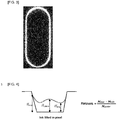
- the ink compositions prepared in Examples and Comparative Examples were injected into the head of a Dimatix Materials Cartridge (Fujifilm), and ink droplets were discharged by nine drops on each pixel (see FIG. 1 ). The solvent was then removed by vacuum drying and heat treatment to form a final ink film. The film image (confirmed by optical microscope) and the profile (confirmed by optical profiler, using Zygo device) were observed for the prepared ink film and evaluated as follows.
- the ink compositions prepared in Examples and Comparative Examples were discharged to the pixel area, and the solvent was removed by vacuum drying and heat treatment. Then, the ink film profile was observed (confirmed by the optical profiler, using Zygo device). The ink was formed to a thickness of 20 nm to 150 nm. Next, the value of (Hmax-Hmin) / Hcenter was evaluated as follows.
Landscapes
- Chemical & Material Sciences (AREA)
- Engineering & Computer Science (AREA)
- Materials Engineering (AREA)
- Organic Chemistry (AREA)
- Life Sciences & Earth Sciences (AREA)
- Wood Science & Technology (AREA)
- Chemical Kinetics & Catalysis (AREA)
- General Chemical & Material Sciences (AREA)
- Physics & Mathematics (AREA)
- Spectroscopy & Molecular Physics (AREA)
- Manufacturing & Machinery (AREA)
- Electroluminescent Light Sources (AREA)
- Inks, Pencil-Leads, Or Crayons (AREA)
- Organic Low-Molecular-Weight Compounds And Preparation Thereof (AREA)
Abstract
Description
- This application claims priority to or the benefit of Korean Patent Application No.
10-2018-0116458 - The present invention relates to an ink composition for an organic light emitting device that can be applied to an inkjet process.
- In general, an organic light emitting phenomenon refers to a phenomenon where electric energy is converted into light energy by using an organic material. The organic light emitting device using the organic light emitting phenomenon has characteristics such as a wide viewing angle, an excellent contrast, a fast response time, an excellent luminance, driving voltage and response speed, and thus many studies have proceeded.
- The organic light emitting device generally has a structure which comprises an anode, a cathode, and an organic material layer interposed between the anode and the cathode. The organic material layer frequently has a multilayered structure that comprises different materials in order to enhance efficiency and stability of the organic light emitting device, and for example, the organic material layer may be formed of a hole injection layer, a hole transport layer, a light emitting layer, an electron transport layer, an electron injection layer and the like. In the structure of the organic light emitting device, if a voltage is applied between two electrodes, the holes are injected from an anode into the organic material layer and the electrons are injected from the cathode into the organic material layer, and when the injected holes and electrons meet each other, an exciton is formed, and light is emitted when the exciton falls to a ground state again.
- Meanwhile, recently, in order to reduce process costs, an organic light emitting device using a solution process, particularly an inkjet process, has been developed instead of a conventional deposition process. In the initial stage of development, attempts have been made to develop organic light emitting devices by coating all organic light emitting device layers by a solution process, but current technology has limitations. Therefore, only HIL, HTL, and EML are processed in a layer device structure by a solution process, and a hybrid process utilizing traditional deposition processes is being studied as a subsequent process.
- When forming a functional layer of the organic light emitting device using an inkjet process, ink must be stably discharged from the nozzle of the head for accuracy, and a uniform and flat film should be formed in the process of being coated and then dried. For example, when ink is coated onto a functional layer-forming region surrounded by a partition and then dried, it is difficult to secure film flatness if the ink film is unevenly solidified. In particular, there are many cases where the film thickness in the center portion may become thicker than the partition side (convex shape) or the film thickness on the partition side may become thicker than the center portion (concave shape).
- Therefore, there is a need to develop an ink composition for an organic light emitting device that can resolve the above problems when applying the inkjet process.
- (Patent Literature 1) Korean Unexamined Patent Publication No.
10-2000-0051826 - It is an object of the present invention to provide an ink composition for an organic light emitting device that can be applied to an inkjet process.
- In order to achieve the above object, one aspect of the present invention provides an ink composition for an organic light emitting device including: 1) a compound represented by the following Chemical Formula 1, 2) a first solvent of aromatic esters having a boiling point of 260 to 400°C, and 3) a second solvent of aliphatic ethers or aliphatic esters having a boiling point of 200 to 400°C, wherein the boiling point of the first solvent is higher than that of the second solvent.

- L and L1 to L4 are each independently a substituted or unsubstituted C1-60 alkylene; or a substituted or unsubstituted C6-60 arylene,
- Ar1 and Ar2 are each independently a substituted or unsubstituted C6-60 aryl; or a substituted or unsubstituted C2-60 heteroaryl containing one or more heteroatoms selected from the group consisting of N, O and S, and
- R1 to R4 are each independently hydrogen, deuterium, a substituted or unsubstituted C1-60 alkyl, a substituted or unsubstituted C1-60 alkoxy, a substituted or unsubstituted C6-60 aryl, or a substituted or unsubstituted C2-60 heteroaryl containing one or more heteroatoms selected from the group consisting of N, 0 and S,
- Y1 to Y4 are each independently hydrogen or -X-A, with the proviso that at least two of Y1 to Y4 are -X-A,
- X is a single bond, 0, or S,
- A is a functional group that can be crosslinked by heat or light,
- n1 and n4 are each an integer of 0 to 4, and
- n2 and n3 are each an integer of 0 to 3.
- The ink composition for forming an organic light emitting device according to the present invention can form a flat film with a smooth surface when dried after forming an ink film by an inkjet process.
-
-
FIG. 1 schematically shows a method for measuring film flatness according to the experimental example of the present invention. -
FIG. 2 shows examples in which a film image is evaluated as O.K according to the experimental example of the present invention. -
FIG. 3 shows examples in which a film image is evaluated as N.G according to the experimental example of the present invention. -
FIG. 4 schematically shows a method for measuring film flatness according to the experimental example of the present invention. - Hereinafter, embodiments of the present invention will be described in more detail to facilitate understanding of the invention.
- As used herein, the notation


- As used herein, the term "substituted or unsubstituted" means being unsubstituted or substituted with one or more substituents selected from the group consisting of deuterium; a halogen group; a nitrile group; a nitro group; a hydroxy group; a carbonyl group; an ester group; an imide group; an amino group; a phosphine oxide group; an alkoxy group; an aryloxy group; an alkylthioxy group; an arylthioxy group; an alkylsulfoxy group; an arylsulfoxy group; a silyl group; a boron group; an alkyl group; a cycloalkyl group; an alkenyl group; an aryl group; an aralkyl group; an aralkenyl group; an alkylaryl group; an alkylamine group; an aralkylamine group; a heteroarylamine group; an arylamine group; an arylphosphine group; or a heterocyclic group containing at least one of N, O and S atoms, or being unsubstituted or substituted with a substituent to which two or more substituents are linked among the substituents exemplified above. For example, "the substituent to which two or more substituents are linked" may be a biphenyl group. That is, the biphenyl group may also be an aryl group and may be interpreted as a substituent to which two phenyl groups are linked.
- In the present specification, the number of carbon atoms of a carbonyl group is not particularly limited, but is preferably 1 to 40. Specifically, the carbonyl group may be a compound having the following structural formulae but is not limited thereto.


- In the present specification, an ester group may have a structure in which oxygen of the ester group may be substituted by a straight-chain, branched-chain, or cyclic alkyl group having 1 to 25 carbon atoms, or an aryl group having 6 to 25 carbon atoms. Specifically, the ester group may be a compound having the following structural formulae, but is not limited thereto.


- In the present specification, the number of carbon atoms of an imide group is not particularly limited, but is preferably 1 to 25. Specifically, the imide group may be a compound having the following structural formulae, but is not limited thereto.


- In the present specification, a silyl group specifically includes a trimethylsilyl group, a triethylsilyl group, a t-butyldimethylsilyl group, a vinyldimethylsilyl group, a propyldimethylsilyl group, a triphenylsilyl group, a diphenylsilyl group, a phenylsilyl group and the like, but is not limited thereto.
- In the present specification, a boron group specifically includes a trimethylboron group, a triethylboron group, a t-butyldimethylboron group, a triphenylboron group, and a phenylboron group, but is not limited thereto.
- In the present specification, examples of a halogen group include fluorine, chlorine, bromine, or iodine.
- In the present specification, the alkyl group may be a straight-chain or branched chain, and the number of carbon atoms thereof is not particularly limited, but is preferably 1 to 40. According to one embodiment, the number of carbon atoms of the alkyl group is 1 to 20. According to another embodiment, the number of carbon atoms of the alkyl group is 1 to 10. According to another embodiment, the number of carbon atoms of the alkyl group is 1 to 6. Specific examples of the alkyl group include methyl, ethyl, propyl, n-propyl, isopropyl, butyl, n-butyl, isobutyl, tert-butyl, sec-butyl, 1-methyl-butyl, 1-ethyl-butyl, pentyl, n-pentyl, isopentyl, neopentyl, tert-pentyl, hexyl, n-hexyl, 1-methylpentyl, 2-methylpentyl, 4-methyl-2-pentyl, 3,3-dimethylbutyl, 2-ethylbutyl, heptyl, n-heptyl, 1-methylhexyl, cyclopentylmethyl, cyclohectylmethyl, octyl, n-octyl, tert-octyl, 1-methylheptyl, 2-ethylhexyl, 2-propylpentyl, n-nonyl, 2,2-dimethylheptyl, 1-ethylpropyl, 1,1-dimethyl-propyl, isohexyl, 2-methylpentyl, 4-methylhexyl, 5-methylhexyl, and the like, but are not limited thereto.
- In the present specification, the alkenyl group may be a straight chain or branched chain, and the number of carbon atoms thereof is not particularly limited, but is preferably 2 to 40. According to one embodiment, the number of carbon atoms of the alkenyl group is 2 to 20. According to another embodiment, the number of carbon atoms of the alkenyl group is 2 to 10. According to still another embodiment, the number of carbon atoms of the alkenyl group is 2 to 6. Specific examples thereof include vinyl, 1-propenyl, isopropenyl, 1-butenyl, 2-butenyl, 3-butenyl, 1-pentenyl, 2-pentenyl, 3-pentenyl, 3-methyl-1-butenyl, 1,3-butadienyl, allyl, 1-phenylvinyl-1-yl, 2-phenylvinyl-1-yl, 2,2-diphenylvinyl-1-yl, 2-phenyl-2-(naphthyl-1-yl)vinyl-1-yl, 2,2-bis(diphenyl-1-yl)vinyl-1-yl, a stilbenyl group, a styrenyl group, and the like, but are not limited thereto.
- In the present specification, a cycloalkyl group is not particularly limited, but the number of carbon atoms thereof is preferably 3 to 60. According to one embodiment, the number of carbon atoms of the cycloalkyl group is 3 to 30. According to another embodiment, the number of carbon atoms of the cycloalkyl group is 3 to 20. According to still another embodiment, the number of carbon atoms of the cycloalkyl group is 3 to 6. Specific examples thereof include cyclopropyl, cyclobutyl, cyclopentyl, 3-methylcyclopentyl, 2,3-dimethylcyclopentyl, cyclohexyl, 3-methylcyclohexyl, 4-methylcyclohexyl, 2,3-dimethylcyclohexyl, 3,4,5-trimethylcyclohexyl, 4-tert-butylcyclohexyl, cycloheptyl, cyclooctyl, and the like, but are not limited thereto.
- In the present specification, an aryl group is not particularly limited, but preferably has 6 to 60 carbon atoms, and may be a monocyclic aryl group or a polycyclic aryl group. According to one embodiment, the number of carbon atoms of the aryl group is 6 to 30. According to one embodiment, the number of carbon atoms of the aryl group is 6 to 20. The aryl group may be a phenyl group, a biphenyl group, a terphenyl group or the like as the monocyclic aryl group, but is not limited thereto. Examples of the polycyclic aryl group include a naphthyl group, an anthracenyl group, a phenanthryl group, a pyrenyl group, a perylenyl group, a chrysenyl group, a fluorenyl group or the like, but is not limited thereto.
- In the present specification, a fluorenyl group may be substituted, and two substituent groups may be connected with each other to form a spiro structure. In the case where the fluorenyl group is substituted,

- In the present specification, a heterocyclic group is a heterocyclic group including one or more of O, N, Si, and S as a heteroatom, and the number of carbon atoms thereof is not particularly limited, but is preferably 2 to 60. Examples of the heterocyclic group include a thiophene group, a furan group, a pyrrole group, an imidazole group, a thiazole group, an oxazole group, an oxadiazole group, a triazole group, a pyridyl group, a bipyridyl group, a pyrimidyl group, a triazine group, an acridyl group, a pyridazine group, a pyrazinyl group, a quinolinyl group, a quinazoline group, a quinoxalinyl group, a phthalazinyl group, a pyridopyrimidinyl group, a pyridopyrazinyl group, a pyrazinopyrazinyl group, an isoquinoline group, an indole group, a carbazole group, a benzoxazole group, a benzimidazole group, a benzothiazole group, a benzocarbazole group, a benzothiophene group, a dibenzothiophene group, a benzofuranyl group, a phenanthroline group, an isoxazolyl group, an thiadiazolyl group, a phenothiazinyl group, a dibenzofuranyl group, and the like, but are not limited thereto.
- In the present specification, the aryl group in the aralkyl group, the aralkenyl group, the alkylaryl group, and the arylamine group is the same as the aforementioned examples of the aryl group. In the present specification, the alkyl group in the aralkyl group, the alkylaryl group and the alkylamine group is the same as the aforementioned examples of the alkyl group. In the present specification, for the heteroaryl in the heteroarylamine, the aforementioned description of the heterocyclic group can be applied. In the present specification, the alkenyl group in the aralkenyl group is the same as the aforementioned examples of the alkenyl group. In the present specification, the aforementioned description of the aryl group may be applied except that the arylene is a divalent group. In the present specification, the aforementioned description of the heterocyclic group can be applied except that the heteroarylene is a divalent group. In the present specification, the aforementioned description of the aryl group or cycloalkyl group can be applied except that the hydrocarbon ring is not a monovalent group but formed by combining two substituent groups. In the present specification, the aforementioned description of the heterocyclic group can be applied, except that the heterocycle is not a monovalent group but formed by combining two substituent groups.
- The compound represented by Chemical Formula 1 is a material that constitutes a functional layer in the organic light emitting device. Also, it has high solvent affinity with a solvent, has solvent orthogonality, and has resistance to a solvent used when forming other layers in addition to the organic material layer containing the aforementnioned compound by a solution process, thereby preventing movement to another layer. In addition, the organic light emitting device including the same may have low driving voltage, high light emitting efficiency, and high lifetime.
- Preferably, A is any one selected from the group consisting of the following:


- T1 is hydrogen; or a substituted or unsubstituted C1-6 alkyl, and
- T2 to T4 are each independently a substituted or unsubstituted C1-6 alkyl.
- Preferably, L is any one selected from the group consisting of the following:


each R is independently hydrogen or C1-10 alkyl. - Preferably, L1 to L4 are each independently C1-10 alkylene, or the following Chemical Formula 1-A or 1-B:


- R11 to R13 are each independently hydrogen, deuterium, a substituted or unsubstituted C1-60 alkyl, a substituted or unsubstituted C1-60 alkoxy, a substituted or unsubstituted C6-60 aryl, or a substituted or unsubstituted C2-60 heteroaryl containing any one or more heteroatoms selected from the group consisting of N, O and S, and
- m1 to m3 are each an integer of 0 to 4.
- Preferably, Ar1 and Ar2 are the same as each other and are phenyl, biphenylyl, naphthyl, phenanthrenyl, dimethylfluorenyl, or diphenylfluorenyl.
- Representative examples of the compound represented by Chemical Formula 1 are as follows:





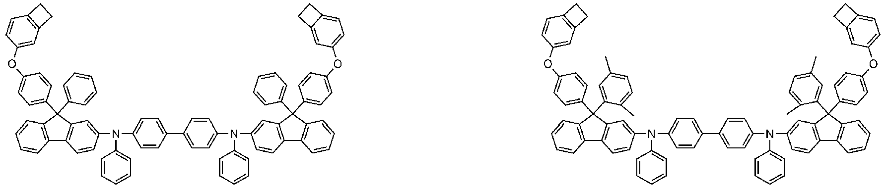



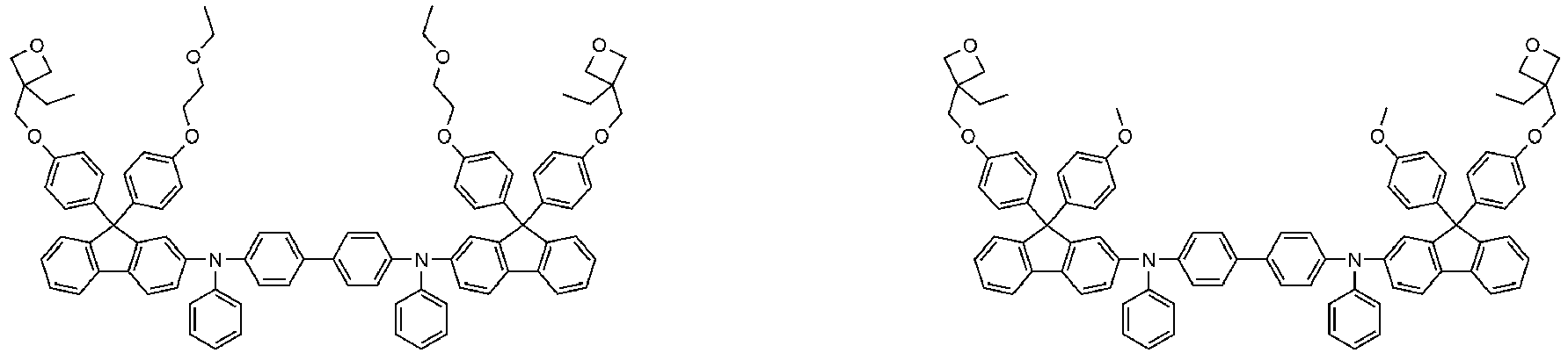


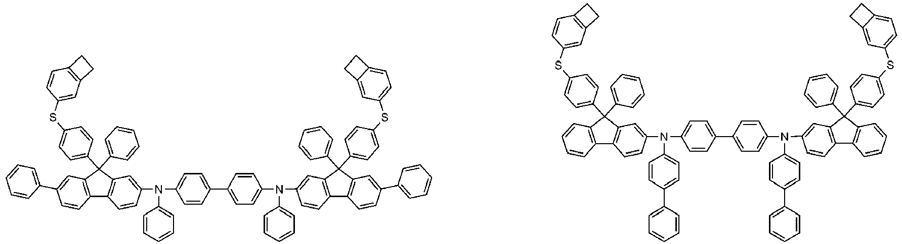





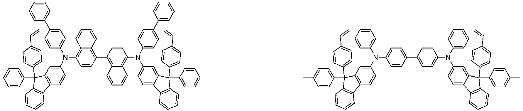






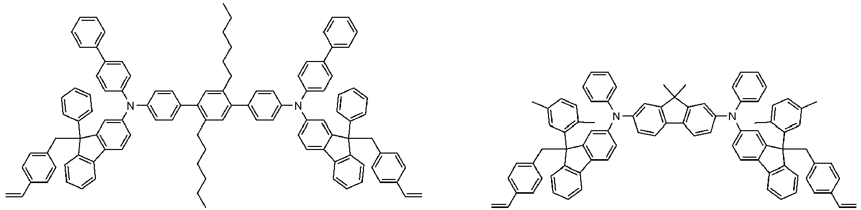

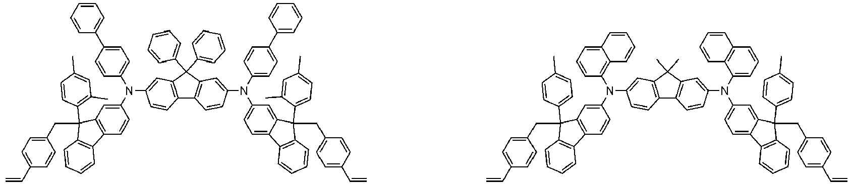


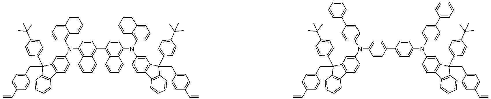


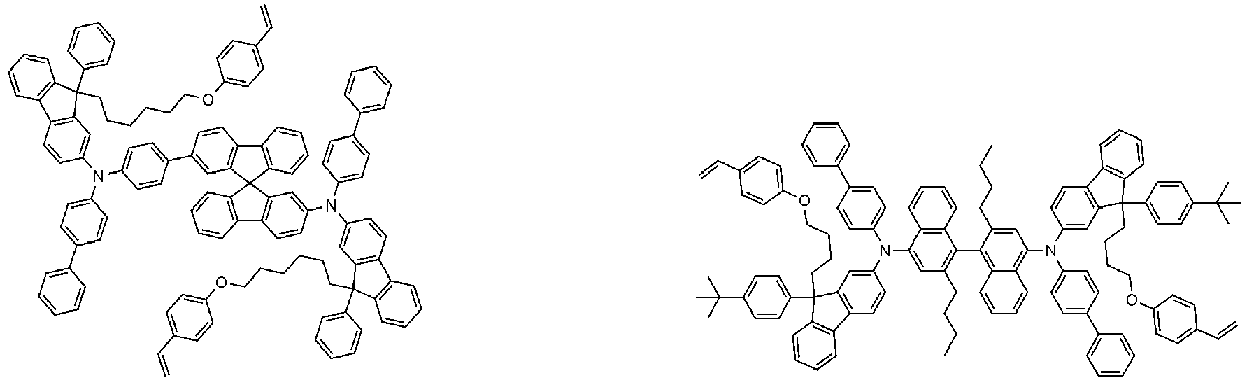


- Meanwhile, the compound represented by Chemical Formula 1 may be prepared in accordance with a method as shown in the following Reaction Scheme 1.

- In Reaction Scheme 1, the remaining substituents excluding Y' are the same as defined above, and Y' is halogen, preferably bromo, or chloro. Reaction Scheme 1 is an amine substitution reaction, which is preferably carried out in the presence of a palladium catalyst and a base, and a reactive


- Preferably, the content of the p-doping material is 0 wt% to 50 wt% with respect to the compound represented by Chemical Formula 1.
- The compound represented by Chemical Formula 1 may form a functional layer by a solution process, but recently, the inkjet printing process is most frequently studied among the solution process. Since the inkjet printing process discharges fine drops, this has the advantage that not only the consumption of materials can be minimized but also precise patterns are possible.
- In order to produce a flat functional layer by a solution process, it is basically necessary to ensure the processability of the ink, the film image and the film flatness at the same time. Since the ink composition is mostly composed of a solvent (minimum 90%, maximum 99.9%) and the ink properties are determined by the solvent, the selection of the solvent is most important.
- The processability of the ink is a property that can be stably discharged without causing a ink drying phenomenon from the nozzle of the inkjet device. For this purpose, it is necessary to select a solvent having a high boiling point characteristic with a sufficiently low vapor pressure. The ink film image is a characteristic of forming a film image with a uniform surface without precipitation/phase separation when undergoing a drying process in the process of producing a functional layer. For this purpose, it is necessary to select a solvent having high solubility characteristics capable of sufficiently dissolving the material of the functional layer and drying characteristics suitable for vacuum drying. In addition, a characteristic required simultaneously with the film image is a film flatness. Since the functional layer is formed of a plurality of laminated structures, each functional layer should be flatly formed so that stable light emission characteristics can be exhibited in the completed organic light emitting device. Therefore, it is important to select a solvent that can simultaneously ensure ink processability, film image, and film flatness from the ink composition. Thus, in the present invention, the above-mentioned characteristics can be realized by using the ink composition containing the first solvent and the second solvent at the same time.
- Although not limited by theory, the first solvent is an aromatic ester, and has a good interaction between the aromatic molecular structure and the compound represented by Chemical Formula 1, which is a functional layer-forming material, thus enhancing the dissolution effect. Moreover, since the first solvent has a higher boiling point than the second solvent, it remains to the end while the ink is dried, thereby obtaining a film image having a uniform surface without precipitation. The second solvent is aliphatic esters, aliphatic ethers, or aromatic ethers, and serves to form a flat functional layer. Meanwhile, the boiling point used herein means the boiling point measured at normal pressure (1 atm).
- Preferably, the first solvent is a compound represented by the following Chemical Formula 2-1, or 2-2:


- X' is a single bond, C1-15 alkylene, or -O-(C1-15 alkylene),
- R'1 is hydrogen, C1-15 alkyl, C1-15 alkoxy, or -COO-(C1-15 alkyl), and
- R'2 is C1-15 alkyl.
- Representative examples of the first solvent include ethyl 4-methoxybenzoate, ethyl 4-ethoxybenzoate, p-tolyl n-octanoate, 2-ethylhexyl benzoate, diethyl phthalate, dimethyl phthalate, 2-phenoxyethyl isobutyrate, 4-(2-acetoxyethoxy)toluene, 2-ethoxyethyl benzoate, 2-isopropoxy benzoate, 2-phenoxyethyl acetate, dimethyl phthalate, or diethyl phthalate.
- Preferably, the second solvent is a compound represented by the following Chemical Formula 3-1, 3-2, or 3-3:


- n is an integer of 1 to 10,
- R"1 is hydrogen or C1-15 alkyl,
- R"2 is hydrogen or C1-15 alkyl, and
- X" is C1-10alkylene.
- Preferably, the second solvent is diethylene glycol butyl methyl ether, diethylene glycol dibutyl ether, tetraethylene glycol monomethyl ether, tetraethylene glycol dimethyl ether, triethylene glycol n-butyl ether, triethylene glycol butylmethyl ether, triethylene glycol monoisopropyl ether, diethylene glycol monohexyl ether, triethylene glycol monoethyl ether, triethylene glycol monomethyl ether, diethylene glycol monobutyl ether, dipropylene glycol n-butyl ether, triethylene glycol dimethyl ether, dipropylene glycol propyl ether, dipropylene glycol methyl ether, diethylene glycol monoethyl ether, tetraethylene glycol monomethyl ether, triethylene glycol, diethylene glycol, amyl n-octanoate, ethyl n-octanoate, isopropyl n-octanoate, propyl n-octanoate, butyl n-octanoate, methyl undecanoate, methyl laurate, methyl tridecanoate, dibutyl malonate, dibutyl oxalate, diethyl succinate, ethyl laurate, methyl myristate, diethyl adipate, diisopropyl adipate, dibutyl adipate, or dodecyl acetate.
- Preferably, the weight ratio of the first solvent and the second solvent is 1:99 to 50:50. More preferably, the weight ratio is 10:90 to 40:60.
- The ink composition according to the present invention described above can be used for the production of a functional layer of an organic light emitting device. The ink composition may be used to produce a functional layer of the organic light emitting device by a solution process, and in particular, an inkjet process may be applied.
- The inkjet process may use a method known in the art, except for using the ink composition according to the present invention described above. As an example, the method may include a step of discharging the ink composition to form an ink film; and a step of drying the ink film. In addition, since the compound represented by Chemical Formula 1 includes a functional group that can be crosslinked by heat or light, it may further include a step of subjecting to heat treatment or light treatment after the aforementioned step.
- Meanwhile, the functional layer which may be formed of the ink composition may be a hole injection layer, a hole transport layer, and a light emitting layer of the organic light emitting device. In addition, since the structure and production method of the organic light emitting device used in the art can be applied except for the functional layer, a detailed description thereof will be omitted.
- Hereinafter, preferred examples are provided to facilitate understanding the present invention. However, these examples are merely provided for a better understanding of the present invention, and the scope of the present invention are not limited thereto.
-

- Toluene was placed in a flask containing Compound 3-1 (1.58 g, 3.74 mmol), N4,N4'-diphenyl-[1,1'-biphenyl]-4,4'-diamine (572 mg, 1.7 mmol), and sodium t-butoxide (980 mg, 10.2 mmol). The flask was immersed in an oil bath at 90°C, and then Pd(PtBu3)2 (43 mg, 0.085 mmol) was added thereto and reacted for 1 hour. Water was added to stop the reaction, the mixture was extracted with dichloromethane, and the organic layer was dried over MgSO4. The organic solvent was removed using a vacuum rotary concentrator, and then the residue was purified by column chromatography to obtain Compound 3 (yield: 55%).
MS[M+H]+ = 1022 -

- Compound 1 was prepared in the same manner as in Preparation Example 1, except that Compound 1-1 was used instead of compound 3-1 and N4,N4'-di(biphenyl-4-yl)biphenyl-4,4'-diamine was used instead of N4,N4'-diphenyl-[1,1'-biphenyl]-4,4'-diamine.
MS[M+H]+= 1374 -

- Compound 2 was prepared in the same manner as in Preparation Example 1, except that Compound 2-1 was used instead of compound 3-1 and N4,N4'-di(biphenyl-4-yl)biphenyl-4,4'-diamine was used instead of N4,N4'-diphenyl-[1,1'-biphenyl]-4,4'-diamine.
MS[M+H]+= 1342 -

- 2-Bromo-9-phenyl-9H-fluorene-9-ol (50 g, 148.3 mmol, 1.0 eq) and phenol (41.8 g, 444.9 mmol, 3.0 eq) were placed in a 500 ml round flask, and dissolved in methanesulfonic acid (200 ml, 0.74 M). The reaction mixture was stirred overnight under reflux. Then, the reaction was stopped with a saturated aqueous NaHCO3 solution, and the organic layer was extracted with ethyl acetate. The organic layer was dried over magnesium sulfate, the solvent was removed and then the product was purified by column chromatography to obtain Intermediate Compound 4-1.
-

- Intermediate 4-1 (30 g, 63.9 mmol, 1.0 eq) and cesium carbonate (41.6 g, 127.8 mmol, 2.0 eq) were dissolved in DMF (120 ml, 0.5 M) in a 500 ml round flask, and the mixture was heated to 50°C and stirred. Then, 4-vinylbenzyl chloride (9.15 ml, 9.75 g, 1.0 eq) was added and stirred at 60°C. After cooling to room temperature, water was added and the reaction was stopped. The organic layer was extracted using ethyl acetate. The organic layer was separated and dried over magnesium sulfate. The solvent was removed and the product was purified by column chromatography to obtain Intermediate Compound 4-2.
-

- Intermediate 4-2 (12.0 g, 20.49 mmol, 2.05 eq), N4,N4'-diphenyl-[1,1'-biphenyl]-4,4'-diamine (3.36 g, 10.0 mmol, 1.0 eq), NaOtBu (3.36 g, 34.99 mmol, 3.5 eq) and Pd(PtBu3)2 (255 mg, 0.5 mmol, 0.05 eq) were dissolved in toluene (100 ml) in a 250 ml round flask and then stirred and reacted under a nitrogen atmosphere. Then, when the reaction was completed, workup was performed with water and ethyl acetate, the organic layer was separated, dried and then filtered. The solvent was then removed with a rotary vacuum evaporator. The resulting crude material was purified by column chromatography and the solvent was removed to obtain Compound 4 (white solid).
MS[M+H]+= 1234 -

- 4-(2-Bromo-9-(4-(tert-butyl)phenyl)-9H-fluoren-9-yl)phenol (50 g, 106.50 mmol, 1.0 eq), 4-bromobenzaldehyde (23.6 g, 127.8 mmol, 1.2 eq) and potassium carbonate (44.2 g, 319.50 mmol, 3.0 eq) were placed in a 500 ml round flask and dissolved in dry pyridine (200 ml, 0.5 M). Then, copper(II) oxide (17.0 g, 213.0 mmol, 2 eq) was slowly added and the mixture was heated to 120°C, and allowed to react under reflux. When the reaction was completed, the reaction was stopped with saturated aqueous NaHCO3 solution, and the organic layer was extracted with ethyl acetate. The organic layer was dried over magnesium sulfate, and then the solvent was removed. The resulting crude was dissolved in dichloromethane and precipitated in ethanol to obtain a solid intermediate compound 5-1.
-

- Anhydrous tetrahydrofuran (50 ml, 0.2 M) was placed in a round flask containing methyltriphenylphosphonium bromide (12.46 g, 34.87 mmol, 2.0 eq), and the round flask was immersed in an ice bath. Potassium tert-butoxide (3.9 g, 34.87 mmol, 2.0 eq) was added in one portion and stirred in an ice bath for 20 minutes. Intermediate Compound 5-1 (10.0 g, 17.44 mmol, 1.0 eq) was dissolved in tetrahydrofuran (30 ml) and then gradually added to the mixture using a dropping funnel. Then, tetrahydrofuran (10 ml) was added to wash the round flask and funnel. Water (50 ml) was added to terminate the reaction, and the organic layer was extracted with ethyl acetate. The organic layer was dried over magnesium sulfate, and then the solvent was removed and the product was purified by column chromatography to obtain Compound 5-2.
-

- Intermediate Compound 5-2 (10.0 g, 17.50 mmol, 2.05 eq), N4,N4'-diphenyl-[1,1'-biphenyl]-4,4'-diamine (2.87 g, 8.53 mmol, 1.0 eq), NaOtBu (2.87 g, 29.86 mmol, 3.5 eq) and Pd(PtBu3)2 (218.0 mg, 0.43 mmol, 0.05 eq) were dissolved in toluene (90 ml) in a 250 ml round flask and then stirred and reacted under a nitrogen atmosphere. Then, when the reaction was completed, workup was performed with water and ethyl acetate, the organic layer was separated, dried and then filtered. The solvent was then removed with a rotary vacuum evaporator. The resulting crude material was purified by column chromatography and the solvent was removed to obtain Compound 5 (white solid).
MS[M+H]+= 1318 -

- 4-(2-Bromo-9-(p-tolyl)-9H-fluoren-9-yl)phenol (15 g, 35.1 mmol, 1.0 eq), potassium carbonate (14.6 g, 105.3 mmol, 3 eq), copper iodide (I) (334.3 mg, 1.76 mmol, 0.05 eq) and 1-butylimidazole (4.4 g, 35.1 mmol, 1.0 eq) were placed in a 250 ml round flask and then dissolved in toluene (175 ml). After the reflux device was installed, the reaction mixture was heated to 120°C and stirred to proceed the reaction. When the reaction was completed, the reaction was stopped with saturated aqueous NaHCO3 solution and worked up with water and ethyl acetate. The organic layer was separated, dried over MgSO4 and filtered. Then, the solvent was removed using a rotary vacuum evaporator, and the resulting crude material was purified by column chromatography to obtain Intermediate Compound 6-1.
-

- Intermediate Compound 6-1 (10.0 g, 18.89 mmol, 2.05 eq), N4,N4'-diphenyl-[1,1'-biphenyl]-4,4'-diamine (3.10 g, 9.21 mmol, 1.0 eq), NaOtBu (3.10 g, 32.24 mmol, 3.5 eq) and Pd(PtBu3)2 (235.1 mg, 0.46 mmol, 0.05 eq) were dissolved in toluene (120 ml) in a 250 ml round flask and then stirred and reacted under a nitrogen atmosphere. Then, when the reaction was completed, workup was performed with water and ethyl acetate, the organic layer was separated, dried and then filtered. The solvent was then removed with a rotary vacuum evaporator. The resulting crude material was purified by column chromatography and the solvent was removed to obtain Compound 6 (white solid).
MS[M+H]+= 1234 - Hereinafter, the solvents used in Examples and Comparative Examples are shown in Table 1 below, and each boiling point is as described in Table 1 below. The following boiling point means the boiling point measured at normal pressure (1 atm).
[Table 1] First solvent Boiling point(° C) Second solvent Boiling point(° C) Ethyl 4-methoxy benzoate 263 Tetraethyleneglycol dimethylether (TeEG DME) 275 Ethyl 4-ethoxy benzoate 275 Triethyleneglycol monobutylether,(TEG MBE) 272 p-tolyl n-octanoate 308 Diethyleneglycol monohexylether (DEG MHE) 260 2-Ethylhexyl Benzoate 313 Diethyleneglycol dibutylether (DEG DBE) 256 Dimethyl phthalate 284 Triethyleneglycol dimethylether (TEG DME) 216 Isoamyl n-octanoate 250 Dibutyl succinate 274 - Dimethyl phthalate as a first solvent and tetraethylene glycol dimethyl ether as a second solvent were mixed in a weight ratio of 1:99, 10:90, 20:80, 30:70, 40:60 and 50:50 to prepare mixed solutions, respectively. 1.6 wt% of Compound 1 prepared above and 0.4 wt% of Compound A represented by Chemical Formula 2 were added to each of the mixed solutions to prepare ink compositions.

- The ink compositions were prepared in the same manner as in Example 1-1, except that each added material was changed as shown in Tables 2 to 7 below. In the following Tables 2 to 7, the doping material is as follows.


[Table 2] Functional layer material p-doping material First solvent Second solvent Ex. 1-1 Com. 1 Com. A Dimethyl phthalate TeEG DME Ex. 1-2 Com. 1 Com. A Dimethyl phthalate TEG MBE Ex. 1-3 Com. 1 Com. B Ethyl 4-methoxybenzoate DEG MHE Ex. 1-4 Com. 1 Com. B Ethyl 4-methoxybenzoate DEG DBE Ex. 1-5 Com. 1 Com. B Ethyl 4-methoxybenzoate TEG DME Ex. 1-6 Com. 1 Com. C Ethyl 4-methoxybenzoate Isoamyl n-octanoate Ex. 1-7 Com. 1 Com. C Dimethyl phthalate Dibutyl succinate Ex. 1-8 Com. 1 Com. A Ethyl 4-ethoxybenzoate TEG MBE Ex. 1-9 Com. 1 Com. B Ethyl 4-ethoxybenzoate DEG MHE Ex. 1-10 Com. 1 Com. B Ethyl 4-ethoxybenzoate DEG DBE Ex. 1-11 Com. 1 Com. B Ethyl 4-ethoxybenzoate TEG DME Ex. 1-12 Com. 1 Com. C Ethyl 4-ethoxybenzoate Isoamyl n-octanoate Ex. 1-13 Com. 1 Com. C Ethyl 4-ethoxybenzoate Dibutyl succinate Ex. 1-14 Com. 1 Com. A 2-Ethylhexyl Benzoate TEG MBE Ex. 1-15 Com. 1 Com. B 2-Ethylhexyl Benzoate DEG MHE Ex. 1-16 Com. 1 Com. B 2-Ethylhexyl Benzoate DEG DBE Ex. 1-17 Com. 1 Com. C 2-Ethylhexyl Benzoate Isoamyl n-octanoate Ex. 1-18 Com. 1 Com. C 2-Ethylhexyl Benzoate Dibutyl succinate Ex. 1-19 Com. 1 Com. A p-tolyl n-octanoate TEG MBE Ex. 1-20 Com. 1 Com. B p-tolyl n-octanoate DEG MHE Ex. 1-21 Com. 1 Com. B p-tolyl n-octanoate DEG DBE Ex. 1-22 Com. 1 Com. C p-tolyl n-octanoate Isoamyl n-octanoate Ex. 1-23 Com. 1 Com. C p-tolyl n-octanoate Dibutyl succinate [Table 3] Functional layer material p-doping material First solvent Second solvent Ex. 2-1 Com. 2 Com. D Dimethyl phthalate TeEG DME Ex. 2-2 Com. 2 Com. D Dimethyl phthalate TEG MBE Ex. 2-3 Com. 2 Com. E Ethyl 4-methoxybenzoate DEG MHE Ex. 2-4 Com. 2 Com. E Ethyl 4-methoxybenzoate DEG DBE Ex. 2-5 Com. 2 Com. E Ethyl 4-methoxybenzoate TEG DME Ex. 2-6 Com. 2 Com. F Ethyl 4-methoxybenzoate Isoamyl n-octanoate Ex. 2-7 Com. 2 Com. F Dimethyl phthalate Dibutyl succinate Ex. 2-8 Com. 2 Com. D Ethyl 4-ethoxybenzoate TEG MBE Ex. 2-9 Com. 2 Com. E Ethyl 4-ethoxybenzoate DEG MHE Ex. 2-10 Com. 2 Com. E Ethyl 4-ethoxybenzoate DEG DBE Ex. 2-11 Com. 2 Com. E Ethyl 4-ethoxybenzoate TEG DME Ex. 2-12 Com. 2 Com. F Ethyl 4-ethoxybenzoate Isoamyl n-octanoate Ex. 2-13 Com. 2 Com. F Ethyl 4-ethoxybenzoate Dibutyl succinate Ex. 2-14 Com. 2 Com. D 2-Ethylhexyl Benzoate TEG MBE Ex. 2-15 Com. 2 Com. E 2-Ethylhexyl Benzoate DEG MHE Ex. 2-16 Com. 2 Com. E 2-Ethylhexyl Benzoate DEG DBE Ex. 2-17 Com. 2 Com. F 2-Ethylhexyl Benzoate Isoamyl n-octanoate Ex. 2-18 Com. 2 Com. F 2-Ethylhexyl Benzoate Dibutyl succinate Ex. 2-19 Com. 2 Com. D p-tolyl n-octanoate TEG MBE Ex. 2-20 Com. 2 Com. E p-tolyl n-octanoate DEG MHE Ex. 2-21 Com. 2 Com. E p-tolyl n-octanoate DEG DBE Ex. 2-22 Com. 2 Com. F p-tolyl n-octanoate Isoamyl n-octanoate Ex. 2-23 Com. 2 Com. F p-tolyl n-octanoate Dibutyl succinate [Table 4] Functional layer material p-doping material First solvent Second solvent Ex. 3-1 Com. 3 Com. C Dimethyl phthalate TeEG DME Ex. 3-2 Com. 3 Com. B Dimethyl phthalate TEG MBE Ex. 3-3 Com. 3 Com. B Ethyl 4-methoxybenzoate DEG MHE Ex. 3-4 Com. 3 Com. B Ethyl 4-methoxybenzoate DEG DBE Ex. 3-5 Com. 3 Com. B Ethyl 4-methoxybenzoate TEG DME Ex. 3-6 Com. 3 Com. B Ethyl 4-methoxybenzoate Isoamyl n-octanoate Ex. 3-7 Com. 3 Com. B Dimethyl phthalate Dibutyl succinate Ex. 3-8 Com. 3 Com. B Ethyl 4-ethoxybenzoate TEG MBE Ex. 3-9 Com. 3 Com. B Ethyl 4-ethoxybenzoate DEG MHE Ex. 3-10 Com. 3 Com. B Ethyl 4-ethoxybenzoate DEG DBE Ex. 3-11 Com. 3 Com. B Ethyl 4-ethoxybenzoate TEG DME Ex. 3-12 Com. 3 Com. B Ethyl 4-ethoxybenzoate Isoamyl n-octanoate Ex. 3-13 Com. 3 Com. B Ethyl 4-ethoxybenzoate Dibutyl succinate Ex. 3-14 Com. 3 Com. B 2-Ethylhexyl Benzoate TEG MBE Ex. 3-15 Com. 3 Com. B 2-Ethylhexyl Benzoate DEG MHE Ex. 3-16 Com. 3 Com. B 2-Ethylhexyl Benzoate DEG DBE Ex. 3-17 Com. 3 Com. B 2-Ethylhexyl Benzoate Isoamyl n-octanoate Ex. 3-18 Com. 3 Com. B 2-Ethylhexyl Benzoate Dibutyl succinate Ex. 3-19 Com. 3 Com. B p-tolyl n-octanoate TEG MBE Ex. 3-20 Com. 3 Com. B p-tolyl n-octanoate DEG MHE Ex. 3-21 Com. 3 Com. B p-tolyl n-octanoate DEG DBE Ex. 3-22 Com. 3 Com. B p-tolyl n-octanoate Isoamyl n-octanoate Ex. 3-23 Com. 3 Com. B p-tolyl n-octanoate Dibutyl succinate [Table 5] Functional layer material p-doping material First solvent Second solvent Ex. 4-1 Com. 4 Com. F Dimethyl phthalate TeEG DME Ex. 4-2 Com. 4 Com. C Dimethyl phthalate TEG MBE Ex. 4-3 Com. 4 Com. C Ethyl 4-methoxybenzoate DEG MHE Ex. 4-4 Com. 4 Com. C Ethyl 4-methoxybenzoate DEG DBE Ex. 4-5 Com. 4 Com. B Ethyl 4-methoxybenzoate TEG DME Ex. 4-6 Com. 4 Com. B Ethyl 4-methoxybenzoate Isoamyl n-octanoate Ex. 4-7 Com. 4 Com. B Dimethyl phthalate Dibutyl succinate Ex. 4-8 Com. 4 Com. C Ethyl 4-ethoxybenzoate TEG MBE Ex. 4-9 Com. 4 Com. C Ethyl 4-ethoxybenzoate DEG MHE Ex. 4-10 Com. 4 Com. C Ethyl 4-ethoxybenzoate DEG DBE Ex. 4-11 Com. 4 Com. B Ethyl 4-ethoxybenzoate TEG DME Ex. 4-12 Com. 4 Com. B Ethyl 4-ethoxybenzoate Isoamyl n-octanoate Ex. 4-13 Com. 4 Com. B Ethyl 4-ethoxybenzoate Dibutyl succinate Ex. 4-14 Com. 4 Com. F 2-Ethylhexyl Benzoate TEG MBE Ex. 4-15 Com. 4 Com. C 2-Ethylhexyl Benzoate DEG MHE Ex. 4-16 Com. 4 Com. C 2-Ethylhexyl Benzoate DEG DBE Ex. 4-17 Com. 4 Com. B 2-Ethylhexyl Benzoate Isoamyl n-octanoate Ex. 4-18 Com. 4 Com. B 2-Ethylhexyl Benzoate Dibutyl succinate Ex. 4-19 Com. 4 Com. F p-tolyl n-octanoate TEG MBE Ex. 4-20 Com. 4 Com. C p-tolyl n-octanoate DEG MHE Ex. 4-21 Com. 4 Com. C p-tolyl n-octanoate DEG DBE Ex. 4-22 Com. 4 Com. B p-tolyl n-octanoate Isoamyl n-octanoate Ex. 4-23 Com. 4 Com. B p-tolyl n-octanoate Dibutyl succinate [Table 6] Functional layer material p-doping material First solvent Second solvent Ex. 5-1 Com. 5 Com. C Dimethyl phthalate TeEG DME Ex. 5-2 Com. 5 Com. B Dimethyl phthalate TEG MBE Ex. 5-3 Com. 5 Com. B Ethyl 4-methoxybenzoate DEG MHE Ex. 5-4 Com. 5 Com. B Ethyl 4-methoxybenzoate DEG DBE Ex. 5-5 Com. 5 Com. B Ethyl 4-methoxybenzoate TEG DME Ex. 5-6 Com. 5 Com. B Ethyl 4-methoxybenzoate Isoamyl n-octanoate Ex. 5-7 Com. 5 Com. B Dimethyl phthalate Dibutyl succinate Ex. 5-8 Com. 5 Com. B Ethyl 4-ethoxybenzoate TEG MBE Ex. 5-9 Com. 5 Com. B Ethyl 4-ethoxybenzoate DEG MHE Ex. 5-10 Com. 5 Com. B Ethyl 4-ethoxybenzoate DEG DBE Ex. 5-11 Com. 5 Com. B Ethyl 4-ethoxybenzoate TEG DME Ex. 5-12 Com. 5 Com. B Ethyl 4-ethoxybenzoate Isoamyl n-octanoate Ex. 5-13 Com. 5 Com. B Ethyl 4-ethoxybenzoate Dibutyl succinate Ex. 5-14 Com. 5 Com. B 2-Ethylhexyl Benzoate TEG MBE Ex. 5-15 Com. 5 Com. B 2-Ethylhexyl Benzoate DEG MHE Ex. 5-16 Com. 5 Com. B 2-Ethylhexyl Benzoate DEG DBE Ex. 5-17 Com. 5 Com. B 2-Ethylhexyl Benzoate Isoamyl n-octanoate Ex. 5-18 Com. 5 Com. B 2-Ethylhexyl Benzoate Dibutyl succinate Ex. 5-19 Com. 5 Com. B p-tolyl n-octanoate TEG MBE Ex. 5-20 Com. 5 Com. B p-tolyl n-octanoate DEG MHE Ex. 5-21 Com. 5 Com. B p-tolyl n-octanoate DEG DBE Ex. 5-22 Com. 5 Com. B p-tolyl n-octanoate Isoamyl n-octanoate Ex. 5-23 Com. 5 Com. B p-tolyl n-octanoate Dibutyl succinate [Table 7] Functional layer material p-doping material First solvent Second solvent Ex. 6-1 Com. 6 Com. F Dimethyl phthalate TeEG DME Ex. 6-2 Com. 6 Com. C Dimethyl phthalate TEG MBE Ex. 6-3 Com. 6 Com. C Ethyl 4-methoxybenzoate DEG MHE Ex. 6-4 Com. 6 Com. C Ethyl 4-methoxybenzoate DEG DBE Ex. 6-5 Com. 6 Com. B Ethyl 4-methoxybenzoate TEG DME Ex. 6-6 Com. 6 Com. B Ethyl 4-methoxybenzoate Isoamyl n-octanoate Ex. 6-7 Com. 6 Com. B Dimethyl phthalate Dibutyl succinate Ex. 6-8 Com. 6 Com. C Ethyl 4-ethoxybenzoate TEG MBE Ex. 6-9 Com. 6 Com. C Ethyl 4-ethoxybenzoate DEG MHE Ex. 6-10 Com. 6 Com. C Ethyl 4-ethoxybenzoate DEG DBE Ex. 6-11 Com. 6 Com. B Ethyl 4-ethoxybenzoate TEG DME Ex. 6-12 Com. 6 Com. B Ethyl 4-ethoxybenzoate Isoamyl n-octanoate Ex. 6-13 Com. 6 Com. B Ethyl 4-ethoxybenzoate Dibutyl succinate Ex. 6-14 Com. 6 Com. F 2-Ethylhexyl Benzoate TEG MBE Ex. 6-15 Com. 6 Com. C 2-Ethylhexyl Benzoate DEG MHE Ex. 6-16 Com. 6 Com. C 2-Ethylhexyl Benzoate DEG DBE Ex. 6-17 Com. 6 Com. B 2-Ethylhexyl Benzoate Isoamyl n-octanoate Ex. 6-18 Com. 6 Com. B 2-Ethylhexyl Benzoate Dibutyl succinate Ex. 6-19 Com. 6 Com. F p-tolyl n-octanoate TEG MBE Ex. 6-20 Com. 6 Com. C p-tolyl n-octanoate DEG MHE Ex. 6-21 Com. 6 Com. C p-tolyl n-octanoate DEG DBE Ex. 6-22 Com. 6 Com. B p-tolyl n-octanoate Isoamyl n-octanoate Ex. 6-23 Com. 6 Com. B p-tolyl n-octanoate Dibutyl succinate - The ink compositions were prepared in the same manner as in Example 1-1, except that only the second solvent was used and each added material was changed as shown in Table 8 below.
[Table 8] Functional layer material p-doping material Solvent(single solvent) Comparative Ex. 1 Com. 1 Com. A TeEG DME Comparative Ex. 2 Com. 1 Com. A TEG MBE Comparative Ex. 3 Com. 1 Com. B DEG MHE Comparative Ex. 4 Com. 1 Com. B DEG DBE Comparative Ex. 5 Com. 1 Com. B TEG DME Comparative Ex. 6 Com. 1 Com. C Isoamyl n-octanoate Comparative Ex. 7 Com. 1 Com. C Dibutyl succinate - The properties of the ink compositions prepared in Examples and Comparative Examples were evaluated through the following experiments.
- The ink compositions prepared in Examples and Comparative Examples were stored in a sealed cartridge at 25°C, atmospheric pressure, and general atmospheric conditions for one month. When the ink condition was visually confirmed, it was evaluated according to the following criteria.
- O: very stable
- X: precipitation of solids, phase separation
- The ink compositions prepared in Examples and Comparative Examples were injected into the head of Dimatix Materials Cartridge (Fujifilm), 10 pL of droplets were discharged, and the discharge images visually observed through an equipment camera were evaluated according to the following criteria.
- Droplet is stably discharged for 20 minutes or more without shaking: O
- Straightness of droplets is slightly inferior: Δ
- Droplet does not discharge: X
- The ink compositions prepared in Examples and Comparative Examples were injected into the head of a Dimatix Materials Cartridge (Fujifilm), and ink droplets were discharged by nine drops on each pixel (see
FIG. 1 ). The solvent was then removed by vacuum drying and heat treatment to form a final ink film. The film image (confirmed by optical microscope) and the profile (confirmed by optical profiler, using Zygo device) were observed for the prepared ink film and evaluated as follows. - X: When foreign matters like grains, sparkling dots, white dots, etc. are observed in the pixel (see
FIG. 2 ) - O: When the above case is not observed (see
FIG. 3 ) - As shown in
FIG. 4 , the ink compositions prepared in Examples and Comparative Examples were discharged to the pixel area, and the solvent was removed by vacuum drying and heat treatment. Then, the ink film profile was observed (confirmed by the optical profiler, using Zygo device). The ink was formed to a thickness of 20 nm to 150 nm. Next, the value of (Hmax-Hmin) / Hcenter was evaluated as follows. - Less than 0.3: 0
- 0.3 or more and less than 0.5: Δ
- 0.5 or more: X
- The results are shown in Tables 9 to 15 below.
[Table 9] Evaluation of ink stability/discharge stability Evaluation of film image/film flatness 1st solvent:2n d solvent 1:9 9 10:9 0 20:8 0 30:7 0 40:6 0 50:5 0 1:9 9 10:9 0 20:8 0 30:7 0 40:6 0 50:5 0 Ex. 1-1 O/O O/O O/O O/O O/O O/O X/O O/O O/O O/O O/O O/O Ex. 1-2 O/O O/O O/O O/O O/O O/O X/O O/O O/O O/O O/O O/O Ex. 1-3 O/O O/O O/O O/O O/O O/O X/O O/O O/O O/O O/Δ O/Δ Ex. 1-4 O/O O/O O/O O/O O/O O/O X/O O/O O/O O/O O/Δ O/Δ Ex. 1-5 O/O O/O O/O O/O O/O O/O O/O O/O O/O O/Δ O/Δ O/Δ Ex. 1-6 O/O O/O O/O O/O O/O O/O X/O O/O O/O O/O O/Δ O/Δ Ex. 1-7 O/O O/O O/O O/O O/O O/O O/O O/O O/O O/O O/O O/O Ex. 1-8 O/O O/O O/O O/O O/O O/O X/O O/O O/O O/O O/O O/O Ex. 1-9 O/O O/O O/O O/O O/O O/O X/O O/O O/O O/O O/Δ O/Δ Ex. 1-10 O/O O/O O/O O/O O/O O/O X/O O/O O/O O/O O/Δ O/Δ Ex. 1-11 O/O O/O O/O O/O O/O O/O O/O O/O O/O O/O O/Δ O/Δ Ex. 1-12 O/O O/O O/O O/O O/O O/O X/O O/O O/O O/O O/Δ O/Δ Ex. 1-13 O/O O/O O/O O/O O/O O/O O/O O/O O/O O/O O/O O/O Ex. 1-14 O/O O/O O/O O/O O/O O/O O/O O/O O/O O/O O/O O/O Ex. 1-15 O/O O/O O/O O/O O/O O/O O/O O/O O/O O/O O/O O/O Ex. 1-16 O/O O/O O/O O/O O/O O/O O/O O/O O/O O/O O/O O/O Ex. 1-17 O/O O/O O/O O/O O/O O/O O/O O/O O/O O/O O/O O/O Ex. 1-18 O/O O/O O/O O/O O/O O/O O/O O/O O/O O/O O/O O/O Ex. 1-19 O/O O/O O/O O/O O/O O/O O/O O/O O/O O/O O/O O/O Ex. 1-20 O/O O/O O/O O/O O/O O/O O/O O/O O/O O/O O/O O/O Ex. 1-21 O/O O/O O/O O/O O/O O/O O/O O/O O/O O/O O/O O/O Ex. 1-22 O/O O/O O/O O/O O/O O/O O/O O/O O/O O/O O/O O/O Ex. 1-23 O/O O/O O/O O/O O/O O/O O/O O/O O/O O/O O/O O/O [Table 10] Evaluation of ink stability/discharge stability Evaluation of film image/film flatness 1st solvent:2n d solvent 1:9 9 10:9 0 20:8 0 30:7 0 40:6 0 50:5 0 1:9 9 10:9 0 20:8 0 30:7 0 40:6 0 50:5 0 Ex. 2-1 O/O O/O O/O O/O O/O O/O X/O O/O O/O O/O O/O O/Δ Ex. 2-2 O/O O/O O/O O/O O/O O/O X/O O/O O/O O/O O/O O/Δ Ex. 2-3 O/O O/O O/O O/O O/O O/O X/O O/O O/O O/O O/Δ O/Δ Ex. 2-4 O/O O/O O/O O/O O/O O/O X/O O/O O/O O/O O/Δ O/Δ Ex. 2-5 O/O O/O O/O O/O O/O O/O O/O O/O O/O O/Δ O/Δ O/Δ Ex. 2-6 O/O O/O O/O O/O O/O O/O X/O O/O O/O O/O O/Δ O/Δ Ex. 2-7 O/O O/O O/O O/O O/O O/O O/O O/O O/O O/O O/O O/O Ex. 2-8 O/O O/O O/O O/O O/O O/O X/O O/O O/O O/O O/O O/Δ Ex. 2-9 O/O O/O O/O O/O O/O O/O X/O O/O O/O O/O O/Δ O/Δ Ex. 2-10 O/O O/O O/O O/O O/O O/O X/O O/O O/O O/O O/Δ O/Δ Ex. 2-11 O/O O/O O/O O/O O/O O/O O/O O/O O/O O/O O/Δ O/Δ Ex. 2-12 O/O O/O O/O O/O O/O O/O X/O O/O O/O O/O O/Δ O/Δ Ex. 2-13 O/O O/O O/O O/O O/O O/O O/O O/O O/O O/O O/O O/O Ex. 2-14 O/O O/O O/O O/O O/O O/O O/O O/O O/O O/O O/O O/O Ex. 2-15 O/O O/O O/O O/O O/O O/O O/O O/O O/O O/O O/O O/O Ex. 2-16 O/O O/O O/O O/O O/O O/O O/O O/O O/O O/O O/O O/O Ex. 2-17 O/O O/O O/O O/O O/O O/O O/O O/O O/O O/O O/O O/O Ex. 2-18 O/O O/O O/O O/O O/O O/O O/O O/O O/O O/O O/O O/O Ex. 2-19 O/O O/O O/O O/O O/O O/O O/O O/O O/O O/O O/O O/O Ex. 2-20 O/O O/O O/O O/O O/O O/O O/O O/O O/O O/O O/O O/O Ex. 2-21 O/O O/O O/O O/O O/O O/O O/O O/O O/O O/O O/O O/O Ex. 2-22 O/O O/O O/O O/O O/O O/O O/O O/O O/O O/O O/O O/O Ex. 2-23 O/O O/O O/O O/O O/O O/O O/O O/O O/O O/O O/O O/O [Table 11] Evaluation of ink stability/discharge stability Evaluation of film image/film flatness 1st solvent:2n d solvent 1:9 9 10:9 0 20:8 0 30:7 0 40:6 0 50:5 0 1:9 9 10:9 0 20:8 0 30:7 0 40:6 0 50:5 0 Ex. 3-1 O/O O/O O/O O/O O/O O/O X/O O/O O/O O/O O/O O/O Ex. 3-2 O/O O/O O/O O/O O/O O/O X/O O/O O/O O/O O/O O/O Ex. 3-3 O/O O/O O/O O/O O/O O/O X/O O/O O/O O/O O/Δ O/Δ Ex. 3-4 O/O O/O O/O O/O O/O O/O X/O O/O O/O O/O O/Δ O/Δ Ex. 3-5 O/O O/O O/O O/O O/O O/O O/O O/O O/O O/Δ O/Δ O/Δ Ex. 3-6 O/O O/O O/O O/O O/O O/O X/O O/O O/O O/O O/Δ O/Δ Ex. 3-7 O/O O/O O/O O/O O/O O/O O/O O/O O/O O/O O/O O/O Ex. 3-8 O/O O/O O/O O/O O/O O/O X/O O/O O/O O/O O/O O/O Ex. 3-9 O/O O/O O/O O/O O/O O/O X/O O/O O/O O/O O/Δ O/Δ Ex. 3-10 O/O O/O O/O O/O O/O O/O X/O O/O O/O O/O O/Δ O/Δ Ex. 3-11 O/O O/O O/O O/O O/O O/O O/O O/O O/O O/O O/Δ O/Δ Ex. 3-12 O/O O/O O/O O/O O/O O/O X/O O/O O/O O/O O/Δ O/Δ Ex. 3-13 O/O O/O O/O O/O O/O O/O O/O O/O O/O O/O O/O O/O Ex. 3-14 O/O O/O O/O O/O O/O O/O O/O O/O O/O O/O O/O O/O Ex. 3-15 O/O O/O O/O O/O O/O O/O O/O O/O O/O O/O O/O O/O Ex. 3-16 O/O O/O O/O O/O O/O O/O O/O O/O O/O O/O O/O O/O Ex. 3-17 O/O O/O O/O O/O O/O O/O O/O O/O O/O O/O O/O O/O Ex. 3-18 O/O O/O O/O O/O O/O O/O O/O O/O O/O O/O O/O O/O Ex. 3-19 O/O O/O O/O O/O O/O O/O O/O O/O O/O O/O O/O O/O Ex. 3-20 O/O O/O O/O O/O O/O O/O O/O O/O O/O O/O O/O O/O Ex. 3-21 O/O O/O O/O O/O O/O O/O O/O O/O O/O O/O O/O O/O Ex. 3-22 O/O O/O O/O O/O O/O O/O O/O O/O O/O O/O O/O O/O Ex. 3-23 O/O O/O O/O O/O O/O O/O O/O O/O O/O O/O O/O O/O [Table 12] Evaluation of ink stability/discharge stability Evaluation of film image/film flatness 1st solvent:2n d solvent 1:9 9 10:9 0 20:8 0 30:7 0 40:6 0 50:5 0 1:9 9 10:9 0 20:8 0 30:7 0 40:6 0 50:5 0 Ex. 4-1 O/O O/O O/O O/O O/O O/O X/O O/O O/O O/O O/O O/O Ex. 4-2 O/O O/O O/O O/O O/O O/O X/O O/O O/O O/O O/O O/O Ex. 4-3 O/O O/O O/O O/O O/O O/O X/O O/O O/O O/O O/Δ O/Δ Ex. 4-4 O/O O/O O/O O/O O/O O/O X/O O/O O/O O/O O/Δ O/Δ Ex. 4-5 O/O O/O O/O O/O O/O O/O O/O O/O O/O O/Δ O/Δ O/Δ Ex. 4-6 O/O O/O O/O O/O O/O O/O X/O O/O O/O O/O O/Δ O/Δ Ex. 4-7 O/O O/O O/O O/O O/O O/O O/O O/O O/O O/O O/O O/O Ex. 4-8 O/O O/O O/O O/O O/O O/O X/O O/O O/O O/O O/O O/O Ex. 4-9 O/O O/O O/O O/O O/O O/O X/O O/O O/O O/O O/Δ O/Δ Ex. 4-10 O/O O/O O/O O/O O/O O/O X/O O/O O/O O/O O/Δ O/Δ Ex. 4-11 O/O O/O O/O O/O O/O O/O O/O O/O O/O O/O O/Δ O/Δ Ex. 4-12 O/O O/O O/O O/O O/O O/O X/O O/O O/O O/O O/Δ O/Δ Ex. 4-13 O/O O/O O/O O/O O/O O/O O/O O/O O/O O/O O/O O/O Ex. 4-14 O/O O/O O/O O/O O/O O/O O/O O/O O/O O/O O/O O/O Ex. 4-15 O/O O/O O/O O/O O/O O/O O/O O/O O/O O/O O/O O/O Ex. 4-16 O/O O/O O/O O/O O/O O/O O/O O/O O/O O/O O/O O/O Ex. 4-17 O/O O/O O/O O/O O/O O/O O/O O/O O/O O/O O/O O/O Ex. 4-18 O/O O/O O/O O/O O/O O/O O/O O/O O/O O/O O/O O/O Ex. 4-19 O/O O/O O/O O/O O/O O/O O/O O/O O/O O/O O/O O/O Ex. 4-20 O/O O/O O/O O/O O/O O/O O/O O/O O/O O/O O/O O/O Ex. 4-21 O/O O/O O/O O/O O/O O/O O/O O/O O/O O/O O/O O/O Ex. 4-22 O/O O/O O/O O/O O/O O/O O/O O/O O/O O/O O/O O/O Ex. 4-23 O/O O/O O/O O/O O/O O/O O/O O/O O/O O/O O/O O/O [Table 13] Evaluation of ink stability/discharge stability Evaluation of film image/film flatness 1st solvent:2n d solvent 1:9 9 10:9 0 20:8 0 30:7 0 40:6 0 50:5 0 1:9 9 10:9 0 20:8 0 30:7 0 40:6 0 50:5 0 Ex. 5-1 O/O O/O O/O O/O O/O O/O X/O O/O O/O O/O O/O O/O Ex. 5-2 O/O O/O O/O O/O O/O O/O X/O O/O O/O O/O O/O O/O Ex. 5-3 O/O O/O O/O O/O O/O O/O X/O O/O O/O O/O O/Δ O/Δ Ex. 5-4 O/O O/O O/O O/O O/O O/O X/O O/O O/O O/O O/Δ O/Δ Ex. 5-5 O/O O/O O/O O/O O/O O/O O/O O/O O/O O/Δ O/Δ O/Δ Ex. 5-6 O/O O/O O/O O/O O/O O/O X/O O/O O/O O/O O/Δ O/Δ Ex. 5-7 O/O O/O O/O O/O O/O O/O O/O O/O O/O O/O O/O O/O Ex. 5-8 O/O O/O O/O O/O O/O O/O X/O O/O O/O O/O O/O O/O Ex. 5-9 O/O O/O O/O O/O O/O O/O X/O O/O O/O O/O O/Δ O/Δ Ex. 5-10 O/O O/O O/O O/O O/O O/O X/O O/O O/O O/O O/Δ O/Δ Ex. 5-11 O/O O/O O/O O/O O/O O/O O/O O/O O/O O/O O/Δ O/Δ Ex. 5-12 O/O O/O O/O O/O O/O O/O X/O O/O O/O O/O O/Δ O/Δ Ex. 5-13 O/O O/O O/O O/O O/O O/O O/O O/O O/O O/O O/O O/O Ex. 5-14 O/O O/O O/O O/O O/O O/O O/O O/O O/O O/O O/O O/O Ex. 5-15 O/O O/O O/O O/O O/O O/O O/O O/O O/O O/O O/O O/O Ex. 5-16 O/O O/O O/O O/O O/O O/O O/O O/O O/O O/O O/O O/O Ex. 5-17 O/O O/O O/O O/O O/O O/O O/O O/O O/O O/O O/O O/O Ex. 5-18 O/O O/O O/O O/O O/O O/O O/O O/O O/O O/O O/O O/O Ex. 5-19 O/O O/O O/O O/O O/O O/O O/O O/O O/O O/O O/O O/O Ex. 5-20 O/O O/O O/O O/O O/O O/O O/O O/O O/O O/O O/O O/O Ex. 5-21 O/O O/O O/O O/O O/O O/O O/O O/O O/O O/O O/O O/O Ex. 5-22 O/O O/O O/O O/O O/O O/O O/O O/O O/O O/O O/O O/O Ex. 5-23 O/O O/O O/O O/O O/O O/O O/O O/O O/O O/O O/O O/O [Table 14] Evaluation of ink stability/discharge stability Evaluation of film image/film flatness 1st solvent:2n d solvent 1:9 9 10:9 0 20:8 0 30:7 0 40:6 0 50:5 0 1:9 9 10:9 0 20:8 0 30:7 0 40:6 0 50:5 0 Ex. 6-1 O/O O/O O/O O/O O/O O/O X/O O/O O/O O/O O/O O/Δ Ex. 6-2 O/O O/O O/O O/O O/O O/O X/O O/O O/O O/O O/O O/Δ Ex. 6-3 O/O O/O O/O O/O O/O O/O X/O O/O O/O O/O O/Δ O/Δ Ex. 6-4 O/O O/O O/O O/O O/O O/O X/O O/O O/O O/O O/Δ O/Δ Ex. 6-5 O/O O/O O/O O/O O/O O/O O/O O/O O/O O/Δ O/Δ O/Δ Ex. 6-6 O/O O/O O/O O/O O/O O/O X/O O/O O/O O/O O/Δ O/Δ Ex. 6-7 O/O O/O O/O O/O O/O O/O O/O O/O O/O O/O O/O O/O Ex. 6-8 O/O O/O O/O O/O O/O O/O X/O O/O O/O O/O O/O O/Δ Ex. 6-9 O/O O/O O/O O/O O/O O/O X/O O/O O/O O/O O/Δ O/Δ Ex. 6-10 O/O O/O O/O O/O O/O O/O X/O O/O O/O O/O O/Δ O/Δ Ex. 6-11 O/O O/O O/O O/O O/O O/O O/O O/O O/O O/O O/Δ O/Δ Ex. 6-12 O/O O/O O/O O/O O/O O/O X/O O/O O/O O/O O/Δ O/Δ Ex. 6-13 O/O O/O O/O O/O O/O O/O O/O O/O O/O O/O O/O O/O Ex. 6-14 O/O O/O O/O O/O O/O O/O O/O O/O O/O O/O O/O O/O Ex. 6-15 O/O O/O O/O O/O O/O O/O O/O O/O O/O O/O O/O O/O Ex. 6-16 O/O O/O O/O O/O O/O O/O O/O O/O O/O O/O O/O O/Δ Ex. 6-17 O/O O/O O/O O/O O/O O/O O/O O/O O/O O/O O/O O/Δ Ex. 6-18 O/O O/O O/O O/O O/O O/O O/O O/O O/O O/O O/O O/O Ex. 6-19 O/O O/O O/O O/O O/O O/O O/O O/O O/O O/O O/O O/O Ex. 6-20 O/O O/O O/O O/O O/O O/O O/O O/O O/O O/O O/O O/O Ex. 6-21 O/O O/O O/O O/O O/O O/O O/O O/O O/O O/O O/O O/O Ex. 6-22 O/O O/O O/O O/O O/O O/O O/O O/O O/O O/O O/O O/Δ Ex. 6-23 O/O O/O O/O O/O O/O O/O O/O O/O O/O O/O O/O O/Δ [Table 15] Evaluation of ink stability Evaluation of discharge stability Evaluation of film image Evaluation of film flatness Comparative Ex. 1 O O X O Comparative Ex. 2 O O X O Comparative Ex. 3 O O X O Comparative Ex. 4 O O X O Comparative Ex. 5 O O X O Comparative Ex. 6 O O X O Comparative Ex. 7 O O X O
Claims (11)
- An ink composition for an organic light emitting device comprising:1) a compound represented by the following Chemical Formula 1,2) a first solvent of aromatic esters having a boiling point of 260 to 400°C, and3) a second solvent of aliphatic ethers or aliphatic esters having a boiling point of 200 to 400°C,wherein the boiling point of the first solvent is higher than that of the second solvent:
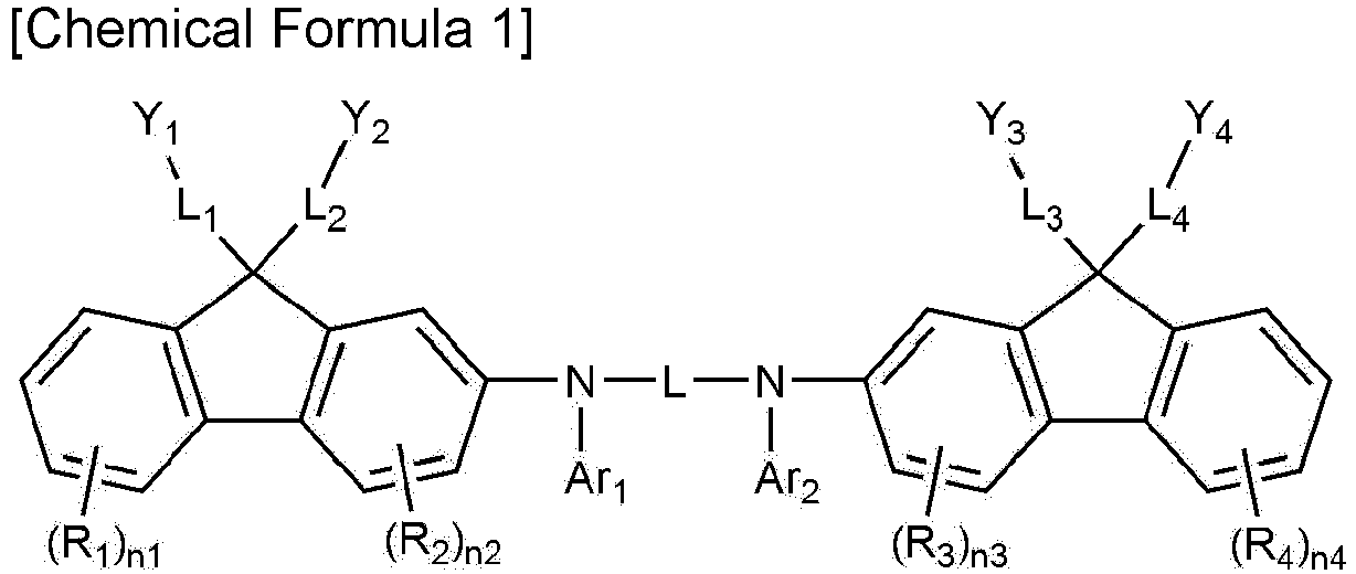 L and L1 to L4 are each independently a substituted or unsubstituted C1-60 alkylene; or a substituted or unsubstituted C6-60 arylene,Ar1 and Ar2 are each independently a substituted or unsubstituted C6-60 aryl; or a substituted or unsubstituted C2-60 heteroaryl containing one or more heteroatoms selected from the group consisting of N, O and S, andR1 to R4 are each independently hydrogen, deuterium, a substituted or unsubstituted C1-60 alkyl, a substituted or unsubstituted C1-60 alkoxy, a substituted or unsubstituted C6-60 aryl, or a substituted or unsubstituted C2-60 heteroaryl containing one or more heteroatoms selected from the group consisting of N, 0 and S,Y1 to Y4 are each independently hydrogen, or -X-A, with the proviso that at least two of Y1 to Y4 are -X-A,X is a single bond, 0, or S,A is a functional group that can be crosslinked by heat or light,n1 and n4 are each an integer of 0 to 4, andn2 and n3 are each an integer of 0 to 3.
 - The ink composition of claim 1, wherein
A is any one selected from the group consisting of the following:


 T1 is hydrogen; or a substituted or unsubstituted C1-6 alkyl, andT2 to T4 are each independently a substituted or unsubstituted C1-6 alkyl.
 - The ink composition of claim 1, wherein
L is any one selected from the group consisting of the following:


each R is independently hydrogen, or C1-10 alkyl. - The ink composition of claim 1, wherein
L1 to L4 are each independently C1-10 alkylene, or the following Chemical Formula 1-A or 1-B:
 R11 to R13 are each independently hydrogen, deuterium, a substituted or unsubstituted C1-60 alkyl, a substituted or unsubstituted C1-60 alkoxy, a substituted or unsubstituted C6-60 aryl, or a substituted or unsubstituted C2-60 heteroaryl containing any one or more heteroatoms selected from the group consisting of N, O and S, andm1 to m3 are each an integer of 0 to 4.
 - The ink composition of claim 1, wherein
Ar1 and Ar2 are the same as each other, and are phenyl, biphenylyl, naphthyl, phenanthrenyl, dimethylfluorenyl, or diphenylfluorenyl. - The ink composition of claim 1, wherein
the compound represented by Chemical Formula 1 is any one selected from the group consisting of the following:


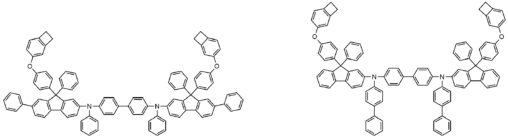


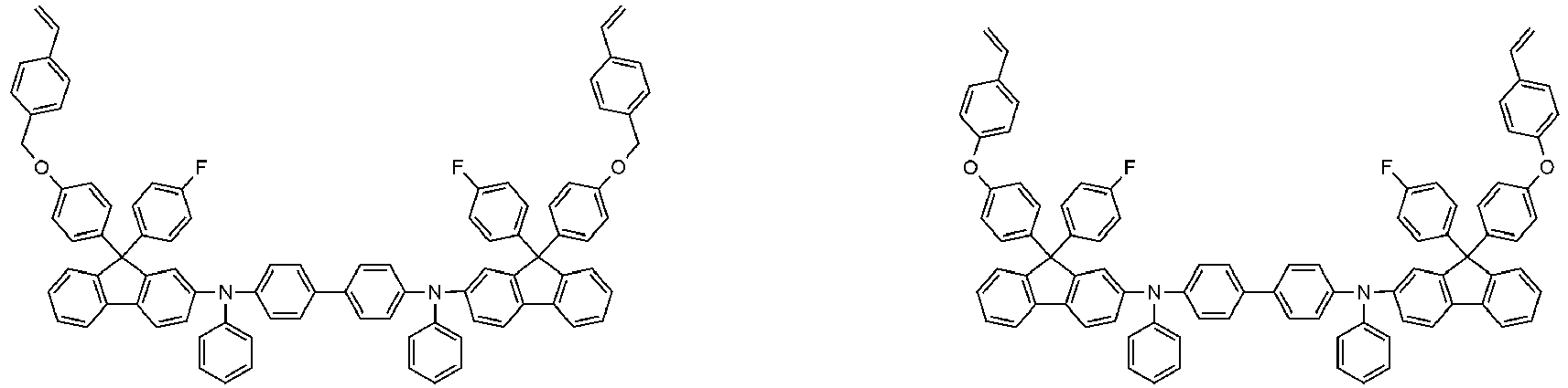


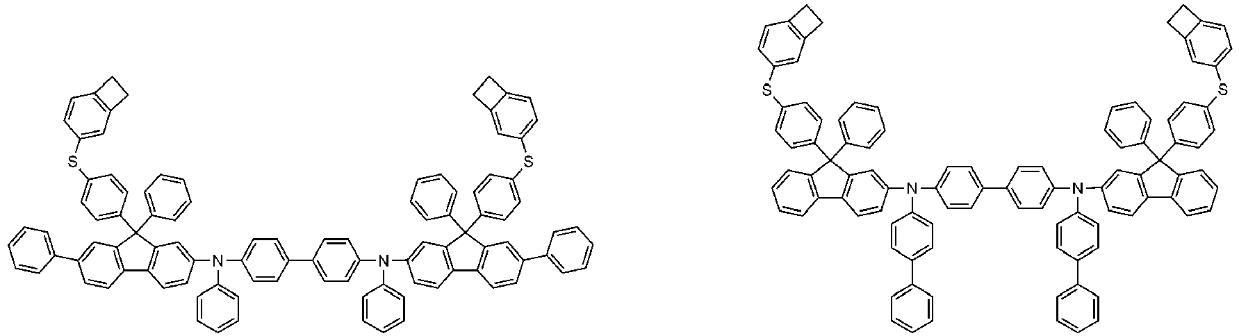
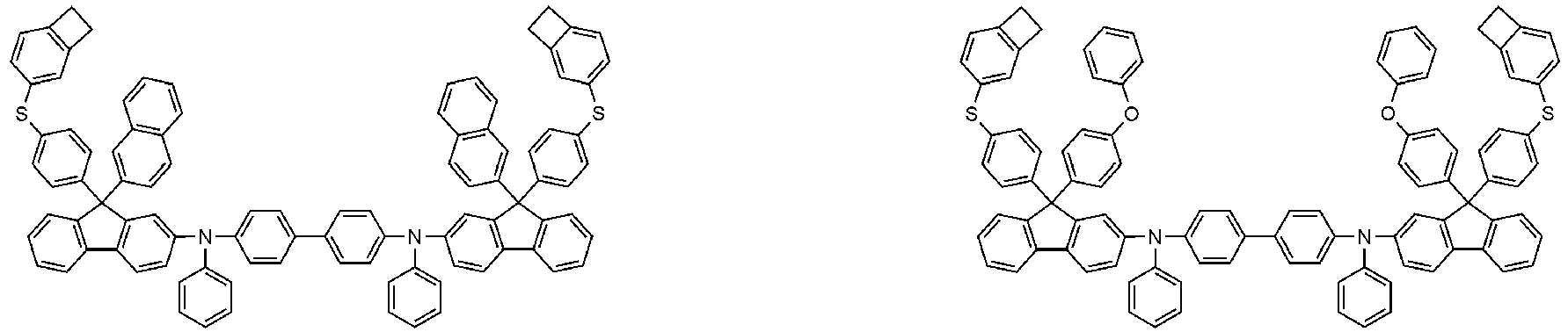


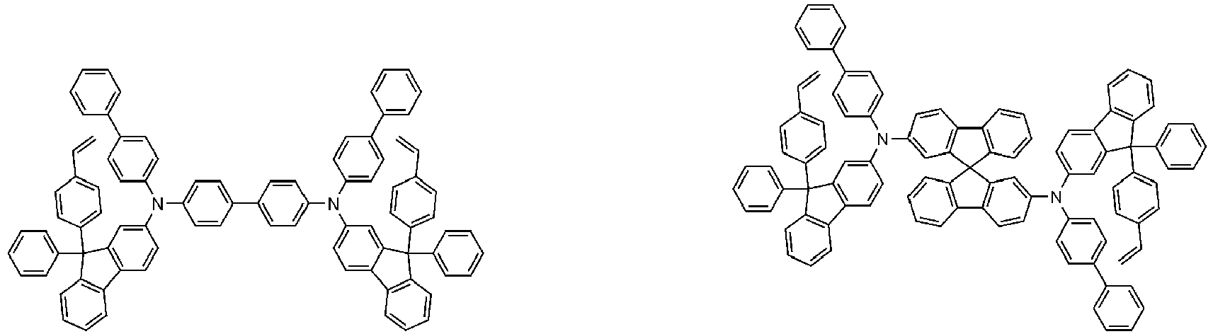











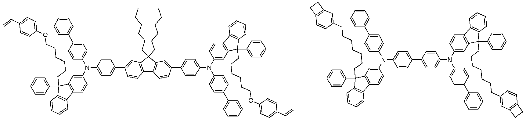


- The ink composition of claim 1, wherein
the first solvent is a compound represented by the following Chemical Formula 2-1, or 2-2:
 X' is a single bond, C1-15 alkylene, or -O-(C1-15 alkylene),R'1 is hydrogen, C1-15 alkyl, C1-15 alkoxy, or -COO-(C1-15 alkyl), andR'2 is C1-15 alkyl.
 - The ink composition of claim 7, wherein
the first solvent is ethyl 4-methoxybenzoate, ethyl 4-ethoxybenzoate, p-tolyl n-octanoate, 2-ethylhexyl benzoate, diethyl phthalate, dimethyl phthalate, 2-phenoxyethyl isobutyrate, 4-(2-acetoxyethoxy)toluene, 2-ethoxyethyl benzoate, 2-isopropoxy benzoate, 2-phenoxyethyl acetate, dimethyl phthalate, or diethyl phthalate. - The ink composition of claim 1, wherein
the second solvent is a compound represented by the following Chemical Formula 3-1, 3-2, or 3-3:

 n is an integer of 1 to 10,R"1 is hydrogen or C1-15 alkyl,R"2 is hydrogen or C1-15 alkyl, andX" is C1-10 alkylene.
 - The ink composition of claim 9, wherein
the second solvent is diethylene glycol butyl methyl ether, diethylene glycol dibutyl ether, tetraethylene glycol monomethyl ether, tetraethylene glycol dimethyl ether, triethylene glycol n-butyl ether, triethylene glycol butylmethyl ether, triethylene glycol monoisopropyl ether, diethylene glycol monohexyl ether, triethylene glycol monoethyl ether, triethylene glycol monomethyl ether, diethylene glycol monobutyl ether, dipropylene glycol n-butyl ether, triethylene glycol dimethyl ether, dipropylene glycol propyl ether, dipropylene glycol methyl ether, diethylene glycol monoethyl ether, tetraethylene glycol monomethyl ether, triethylene glycol, diethylene glycol, amyl n-octanoate, ethyl n-octanoate, isopropyl n-octanoate, propyl n-octanoate, butyl n-octanoate, methyl undecanoate, methyl laurate, methyl tridecanoate, dibutyl malonate, dibutyl oxalate, diethyl succinate, ethyl laurate, methyl myristate, diethyl adipate, diisopropyl adipate, dibutyl adipate, or dodecyl acetate. - The ink composition of claim 1, wherein
the weight ratio of the first solvent and the second solvent is 1:99 to 50:50.
Applications Claiming Priority (2)
| Application Number | Priority Date | Filing Date | Title |
|---|---|---|---|
| KR1020180116458A KR102217266B1 (en) | 2018-09-28 | 2018-09-28 | Ink composition for organic light emitting device |
| PCT/KR2019/012638 WO2020067800A1 (en) | 2018-09-28 | 2019-09-27 | Ink composition for organic light emitting device |
Publications (3)
| Publication Number | Publication Date |
|---|---|
| EP3789464A1 true EP3789464A1 (en) | 2021-03-10 |
| EP3789464A4 EP3789464A4 (en) | 2021-07-28 |
| EP3789464B1 EP3789464B1 (en) | 2022-03-30 |
Family
ID=69953079
Family Applications (1)
| Application Number | Title | Priority Date | Filing Date |
|---|---|---|---|
| EP19866928.5A Active EP3789464B1 (en) | 2018-09-28 | 2019-09-27 | Ink composition for organic light emitting device |
Country Status (7)
| Country | Link |
|---|---|
| US (1) | US11807767B2 (en) |
| EP (1) | EP3789464B1 (en) |
| JP (1) | JP7106193B2 (en) |
| KR (1) | KR102217266B1 (en) |
| CN (1) | CN112154191B (en) |
| TW (1) | TWI707924B (en) |
| WO (1) | WO2020067800A1 (en) |
Families Citing this family (8)
| Publication number | Priority date | Publication date | Assignee | Title |
|---|---|---|---|---|
| KR102182179B1 (en) | 2018-03-16 | 2020-11-24 | 주식회사 엘지화학 | Ink composition and method of manufacturing organic light emitting device |
| US20220064101A1 (en) * | 2019-07-24 | 2022-03-03 | Lg Chem, Ltd. | Novel Compound and Organic Light Emitting Device Comprising the Same |
| KR102681967B1 (en) * | 2020-08-14 | 2024-07-05 | 주식회사 엘지화학 | Organic light emitting device |
| KR102922671B1 (en) * | 2020-08-28 | 2026-02-03 | 주식회사 엘지화학 | Novel compound, coating composition comprising same, organic light emitting device using same and method of manufacturing same |
| KR102680194B1 (en) * | 2020-09-10 | 2024-07-01 | 주식회사 엘지화학 | Organic light emitting device |
| US20230422604A1 (en) * | 2021-01-11 | 2023-12-28 | Lg Chem, Ltd. | Compound, Coating Composition Comprising Same, Organic Light-Emitting Device Using Same And Manufacturing Method Therefor |
| JP7707415B2 (en) * | 2021-09-14 | 2025-07-14 | エルジー・ケム・リミテッド | Ink composition, organic layer containing same, and organic light-emitting device containing same |
| WO2024096610A1 (en) * | 2022-11-04 | 2024-05-10 | 주식회사 엘지화학 | Ink composition, organic material layer comprising same, and organic light-emitting device comprising same |
Family Cites Families (20)
| Publication number | Priority date | Publication date | Assignee | Title |
|---|---|---|---|---|
| KR100430549B1 (en) | 1999-01-27 | 2004-05-10 | 주식회사 엘지화학 | New organomattalic complex molecule for the fabrication of organic light emitting diodes |
| KR100817128B1 (en) | 2001-12-31 | 2008-03-27 | 엘지.필립스 엘시디 주식회사 | Solvent for organic light emitting layer film formation |
| CN101542769B (en) | 2007-04-06 | 2012-04-25 | 出光兴产株式会社 | organic electroluminescent element |
| JP5259139B2 (en) * | 2007-08-31 | 2013-08-07 | 三菱化学株式会社 | Composition for organic electroluminescent device, organic electroluminescent device, and method for producing organic electroluminescent device |
| KR20100003632A (en) | 2008-07-01 | 2010-01-11 | 덕산하이메탈(주) | Novel biphenyl derivatives and electroluminescent device comprising same |
| US20130252351A1 (en) | 2011-09-16 | 2013-09-26 | Kateeva, Inc | Film-forming formulations for substrate printing |
| US8906752B2 (en) | 2011-09-16 | 2014-12-09 | Kateeva, Inc. | Polythiophene-containing ink compositions for inkjet printing |
| EP2764518A1 (en) | 2011-10-04 | 2014-08-13 | Plextronics, Inc. | Improved doping methods for hole injection and transport layers |
| KR102098061B1 (en) | 2012-03-19 | 2020-04-08 | 덕산네오룩스 주식회사 | Compound for organic electronic element, organic electronic element using the same, and a electronic device thereof |
| JP6015073B2 (en) | 2012-04-02 | 2016-10-26 | セイコーエプソン株式会社 | Functional layer forming ink and light emitting device manufacturing method |
| JP6225413B2 (en) | 2012-11-16 | 2017-11-08 | セイコーエプソン株式会社 | Functional layer forming ink, ink container, ejection device, functional layer forming method, organic EL element manufacturing method |
| KR102117603B1 (en) * | 2014-02-10 | 2020-06-01 | 덕산네오룩스 주식회사 | Compound for organic electronic element, organic electronic element using the same, and an electronic device thereof |
| JP6578629B2 (en) | 2014-03-24 | 2019-09-25 | セイコーエプソン株式会社 | Functional layer forming ink and light emitting device manufacturing method |
| JP6550830B2 (en) | 2015-03-25 | 2019-07-31 | セイコーエプソン株式会社 | Composition for forming functional layer, method for producing composition for forming functional layer, method for producing organic EL element, organic EL device, electronic device |
| EP4084109A1 (en) * | 2015-12-15 | 2022-11-02 | Merck Patent GmbH | Esters containing aromatic groups as solvents for organic electronic formulations |
| CN105733562B (en) * | 2016-03-25 | 2019-03-05 | 石家庄诚志永华显示材料有限公司 | A series of fluorene derivative luminescent materials |
| KR102126602B1 (en) | 2016-04-22 | 2020-06-24 | 주식회사 엘지화학 | Carbazole derivatives and organic light emitting diode using the same |
| KR102138404B1 (en) | 2016-07-15 | 2020-07-27 | 주식회사 엘지화학 | Carbazole derivatives, organic light emitting diode using the same and method of manufacturing the same |
| EP3495344B1 (en) | 2016-11-25 | 2021-09-29 | LG Chem, Ltd. | Fluorene derivative, organic light emitting device using same, and manufacturing method therefor |
| JP6820055B2 (en) * | 2017-02-28 | 2021-01-27 | エルジー・ケム・リミテッド | Fluorene compounds, organic light emitting devices using them, and methods for manufacturing them |
-
2018
- 2018-09-28 KR KR1020180116458A patent/KR102217266B1/en active Active
-
2019
- 2019-09-27 CN CN201980034243.8A patent/CN112154191B/en active Active
- 2019-09-27 WO PCT/KR2019/012638 patent/WO2020067800A1/en not_active Ceased
- 2019-09-27 EP EP19866928.5A patent/EP3789464B1/en active Active
- 2019-09-27 TW TW108135261A patent/TWI707924B/en active
- 2019-09-27 US US17/254,058 patent/US11807767B2/en active Active
- 2019-09-27 JP JP2020565413A patent/JP7106193B2/en active Active
Also Published As
| Publication number | Publication date |
|---|---|
| TWI707924B (en) | 2020-10-21 |
| WO2020067800A1 (en) | 2020-04-02 |
| EP3789464B1 (en) | 2022-03-30 |
| JP7106193B2 (en) | 2022-07-26 |
| CN112154191A (en) | 2020-12-29 |
| US20210277269A1 (en) | 2021-09-09 |
| KR102217266B1 (en) | 2021-02-17 |
| TW202026369A (en) | 2020-07-16 |
| US11807767B2 (en) | 2023-11-07 |
| CN112154191B (en) | 2022-11-08 |
| EP3789464A4 (en) | 2021-07-28 |
| JP2021523973A (en) | 2021-09-09 |
| KR20200036610A (en) | 2020-04-07 |
Similar Documents
| Publication | Publication Date | Title |
|---|---|---|
| EP3789464B1 (en) | Ink composition for organic light emitting device | |
| CN111164777B (en) | Organic light emitting device | |
| EP3336159B1 (en) | Organic light-emitting element | |
| JP6946269B2 (en) | Metal complex | |
| EP3477720B1 (en) | Organic light emitting element | |
| EP3564249A1 (en) | Novel compound and organic light emitting device using same | |
| EP3392242A1 (en) | Novel heterocyclic compound and organic light-emitting device using same | |
| CN110267942B (en) | New heterocyclic compounds and organic light-emitting devices using them | |
| DE112019003171T5 (en) | MULTIPLE HOST MATERIALS AND THIS COMPREHENSIVE ORGANIC ELECTROLUMINESCENT DEVICE | |
| EP3415585B1 (en) | Organic light-emitting element | |
| WO2012086170A1 (en) | Aromatic heterocycle derivative and organic electroluminescent element using same | |
| KR20110086043A (en) | Host Materials for Light Emitting Diodes | |
| CN115667248B (en) | Novel compound and organic light emitting device comprising the same | |
| KR20190085070A (en) | Crosslinked triarylamine for electronic devices | |
| EP3539953A1 (en) | Novel compound and organic light-emitting device using same | |
| US11377570B2 (en) | Ink composition for organic light emitting device | |
| KR102651100B1 (en) | Ink composition for organic light emitting device | |
| CN107210378B (en) | Charge-transporting varnish, charge-transporting film and organic electroluminescent device | |
| CN116134030A (en) | Novel compound and organic light-emitting device containing it | |
| CN115135652B (en) | Novel compound and organic light emitting device including the same | |
| EP4371989A1 (en) | Organic compound containing heterocyclic ring, and mixture and organic electronic device | |
| CN121219282A (en) | New compounds and organic light-emitting devices containing them | |
| CN120957985A (en) | New compounds and organic light-emitting devices containing them | |
| KR20210022421A (en) | Organic light emitting device |
Legal Events
| Date | Code | Title | Description |
|---|---|---|---|
| STAA | Information on the status of an ep patent application or granted ep patent |
Free format text: STATUS: THE INTERNATIONAL PUBLICATION HAS BEEN MADE |
|
| PUAI | Public reference made under article 153(3) epc to a published international application that has entered the european phase |
Free format text: ORIGINAL CODE: 0009012 |
|
| STAA | Information on the status of an ep patent application or granted ep patent |
Free format text: STATUS: REQUEST FOR EXAMINATION WAS MADE |
|
| 17P | Request for examination filed |
Effective date: 20201203 |
|
| AK | Designated contracting states |
Kind code of ref document: A1 Designated state(s): AL AT BE BG CH CY CZ DE DK EE ES FI FR GB GR HR HU IE IS IT LI LT LU LV MC MK MT NL NO PL PT RO RS SE SI SK SM TR |
|
| AX | Request for extension of the european patent |
Extension state: BA ME |
|
| A4 | Supplementary search report drawn up and despatched |
Effective date: 20210628 |
|
| RIC1 | Information provided on ipc code assigned before grant |
Ipc: C09D 11/38 20140101AFI20210622BHEP Ipc: C09D 11/36 20140101ALI20210622BHEP Ipc: H01L 51/00 20060101ALI20210622BHEP |
|
| GRAP | Despatch of communication of intention to grant a patent |
Free format text: ORIGINAL CODE: EPIDOSNIGR1 |
|
| STAA | Information on the status of an ep patent application or granted ep patent |
Free format text: STATUS: GRANT OF PATENT IS INTENDED |
|
| RIC1 | Information provided on ipc code assigned before grant |
Ipc: C09D 11/50 20140101ALI20211103BHEP Ipc: C09D 11/328 20140101ALI20211103BHEP Ipc: H01L 51/00 20060101ALI20211103BHEP Ipc: C09D 11/36 20140101ALI20211103BHEP Ipc: C09D 11/38 20140101AFI20211103BHEP |
|
| DAV | Request for validation of the european patent (deleted) | ||
| DAX | Request for extension of the european patent (deleted) | ||
| INTG | Intention to grant announced |
Effective date: 20211130 |
|
| GRAS | Grant fee paid |
Free format text: ORIGINAL CODE: EPIDOSNIGR3 |
|
| GRAA | (expected) grant |
Free format text: ORIGINAL CODE: 0009210 |
|
| STAA | Information on the status of an ep patent application or granted ep patent |
Free format text: STATUS: THE PATENT HAS BEEN GRANTED |
|
| AK | Designated contracting states |
Kind code of ref document: B1 Designated state(s): AL AT BE BG CH CY CZ DE DK EE ES FI FR GB GR HR HU IE IS IT LI LT LU LV MC MK MT NL NO PL PT RO RS SE SI SK SM TR |
|
| REG | Reference to a national code |
Ref country code: GB Ref legal event code: FG4D |
|
| REG | Reference to a national code |
Ref country code: CH Ref legal event code: EP |
|
| REG | Reference to a national code |
Ref country code: DE Ref legal event code: R096 Ref document number: 602019013217 Country of ref document: DE |
|
| REG | Reference to a national code |
Ref country code: AT Ref legal event code: REF Ref document number: 1479181 Country of ref document: AT Kind code of ref document: T Effective date: 20220415 |
|
| REG | Reference to a national code |
Ref country code: IE Ref legal event code: FG4D |
|
| REG | Reference to a national code |
Ref country code: LT Ref legal event code: MG9D |
|
| PG25 | Lapsed in a contracting state [announced via postgrant information from national office to epo] |
Ref country code: SE Free format text: LAPSE BECAUSE OF FAILURE TO SUBMIT A TRANSLATION OF THE DESCRIPTION OR TO PAY THE FEE WITHIN THE PRESCRIBED TIME-LIMIT Effective date: 20220330 Ref country code: RS Free format text: LAPSE BECAUSE OF FAILURE TO SUBMIT A TRANSLATION OF THE DESCRIPTION OR TO PAY THE FEE WITHIN THE PRESCRIBED TIME-LIMIT Effective date: 20220330 Ref country code: NO Free format text: LAPSE BECAUSE OF FAILURE TO SUBMIT A TRANSLATION OF THE DESCRIPTION OR TO PAY THE FEE WITHIN THE PRESCRIBED TIME-LIMIT Effective date: 20220630 Ref country code: LT Free format text: LAPSE BECAUSE OF FAILURE TO SUBMIT A TRANSLATION OF THE DESCRIPTION OR TO PAY THE FEE WITHIN THE PRESCRIBED TIME-LIMIT Effective date: 20220330 Ref country code: HR Free format text: LAPSE BECAUSE OF FAILURE TO SUBMIT A TRANSLATION OF THE DESCRIPTION OR TO PAY THE FEE WITHIN THE PRESCRIBED TIME-LIMIT Effective date: 20220330 Ref country code: BG Free format text: LAPSE BECAUSE OF FAILURE TO SUBMIT A TRANSLATION OF THE DESCRIPTION OR TO PAY THE FEE WITHIN THE PRESCRIBED TIME-LIMIT Effective date: 20220630 |
|
| REG | Reference to a national code |
Ref country code: NL Ref legal event code: MP Effective date: 20220330 |
|
| REG | Reference to a national code |
Ref country code: AT Ref legal event code: MK05 Ref document number: 1479181 Country of ref document: AT Kind code of ref document: T Effective date: 20220330 |
|
| PG25 | Lapsed in a contracting state [announced via postgrant information from national office to epo] |
Ref country code: LV Free format text: LAPSE BECAUSE OF FAILURE TO SUBMIT A TRANSLATION OF THE DESCRIPTION OR TO PAY THE FEE WITHIN THE PRESCRIBED TIME-LIMIT Effective date: 20220330 Ref country code: GR Free format text: LAPSE BECAUSE OF FAILURE TO SUBMIT A TRANSLATION OF THE DESCRIPTION OR TO PAY THE FEE WITHIN THE PRESCRIBED TIME-LIMIT Effective date: 20220701 Ref country code: FI Free format text: LAPSE BECAUSE OF FAILURE TO SUBMIT A TRANSLATION OF THE DESCRIPTION OR TO PAY THE FEE WITHIN THE PRESCRIBED TIME-LIMIT Effective date: 20220330 |
|
| PG25 | Lapsed in a contracting state [announced via postgrant information from national office to epo] |
Ref country code: NL Free format text: LAPSE BECAUSE OF FAILURE TO SUBMIT A TRANSLATION OF THE DESCRIPTION OR TO PAY THE FEE WITHIN THE PRESCRIBED TIME-LIMIT Effective date: 20220330 |
|
| PG25 | Lapsed in a contracting state [announced via postgrant information from national office to epo] |
Ref country code: SM Free format text: LAPSE BECAUSE OF FAILURE TO SUBMIT A TRANSLATION OF THE DESCRIPTION OR TO PAY THE FEE WITHIN THE PRESCRIBED TIME-LIMIT Effective date: 20220330 Ref country code: SK Free format text: LAPSE BECAUSE OF FAILURE TO SUBMIT A TRANSLATION OF THE DESCRIPTION OR TO PAY THE FEE WITHIN THE PRESCRIBED TIME-LIMIT Effective date: 20220330 Ref country code: RO Free format text: LAPSE BECAUSE OF FAILURE TO SUBMIT A TRANSLATION OF THE DESCRIPTION OR TO PAY THE FEE WITHIN THE PRESCRIBED TIME-LIMIT Effective date: 20220330 Ref country code: PT Free format text: LAPSE BECAUSE OF FAILURE TO SUBMIT A TRANSLATION OF THE DESCRIPTION OR TO PAY THE FEE WITHIN THE PRESCRIBED TIME-LIMIT Effective date: 20220801 Ref country code: ES Free format text: LAPSE BECAUSE OF FAILURE TO SUBMIT A TRANSLATION OF THE DESCRIPTION OR TO PAY THE FEE WITHIN THE PRESCRIBED TIME-LIMIT Effective date: 20220330 Ref country code: EE Free format text: LAPSE BECAUSE OF FAILURE TO SUBMIT A TRANSLATION OF THE DESCRIPTION OR TO PAY THE FEE WITHIN THE PRESCRIBED TIME-LIMIT Effective date: 20220330 Ref country code: CZ Free format text: LAPSE BECAUSE OF FAILURE TO SUBMIT A TRANSLATION OF THE DESCRIPTION OR TO PAY THE FEE WITHIN THE PRESCRIBED TIME-LIMIT Effective date: 20220330 Ref country code: AT Free format text: LAPSE BECAUSE OF FAILURE TO SUBMIT A TRANSLATION OF THE DESCRIPTION OR TO PAY THE FEE WITHIN THE PRESCRIBED TIME-LIMIT Effective date: 20220330 |
|
| PG25 | Lapsed in a contracting state [announced via postgrant information from national office to epo] |
Ref country code: PL Free format text: LAPSE BECAUSE OF FAILURE TO SUBMIT A TRANSLATION OF THE DESCRIPTION OR TO PAY THE FEE WITHIN THE PRESCRIBED TIME-LIMIT Effective date: 20220330 Ref country code: IS Free format text: LAPSE BECAUSE OF FAILURE TO SUBMIT A TRANSLATION OF THE DESCRIPTION OR TO PAY THE FEE WITHIN THE PRESCRIBED TIME-LIMIT Effective date: 20220730 Ref country code: AL Free format text: LAPSE BECAUSE OF FAILURE TO SUBMIT A TRANSLATION OF THE DESCRIPTION OR TO PAY THE FEE WITHIN THE PRESCRIBED TIME-LIMIT Effective date: 20220330 |
|
| REG | Reference to a national code |
Ref country code: DE Ref legal event code: R097 Ref document number: 602019013217 Country of ref document: DE |
|
| PG25 | Lapsed in a contracting state [announced via postgrant information from national office to epo] |
Ref country code: DK Free format text: LAPSE BECAUSE OF FAILURE TO SUBMIT A TRANSLATION OF THE DESCRIPTION OR TO PAY THE FEE WITHIN THE PRESCRIBED TIME-LIMIT Effective date: 20220330 |
|
| PLBE | No opposition filed within time limit |
Free format text: ORIGINAL CODE: 0009261 |
|
| STAA | Information on the status of an ep patent application or granted ep patent |
Free format text: STATUS: NO OPPOSITION FILED WITHIN TIME LIMIT |
|
| 26N | No opposition filed |
Effective date: 20230103 |
|
| PG25 | Lapsed in a contracting state [announced via postgrant information from national office to epo] |
Ref country code: MC Free format text: LAPSE BECAUSE OF FAILURE TO SUBMIT A TRANSLATION OF THE DESCRIPTION OR TO PAY THE FEE WITHIN THE PRESCRIBED TIME-LIMIT Effective date: 20220330 |
|
| REG | Reference to a national code |
Ref country code: CH Ref legal event code: PL |
|
| REG | Reference to a national code |
Ref country code: BE Ref legal event code: MM Effective date: 20220930 |
|
| PG25 | Lapsed in a contracting state [announced via postgrant information from national office to epo] |
Ref country code: SI Free format text: LAPSE BECAUSE OF FAILURE TO SUBMIT A TRANSLATION OF THE DESCRIPTION OR TO PAY THE FEE WITHIN THE PRESCRIBED TIME-LIMIT Effective date: 20220330 |
|
| PG25 | Lapsed in a contracting state [announced via postgrant information from national office to epo] |
Ref country code: LU Free format text: LAPSE BECAUSE OF NON-PAYMENT OF DUE FEES Effective date: 20220927 |
|
| PG25 | Lapsed in a contracting state [announced via postgrant information from national office to epo] |
Ref country code: LI Free format text: LAPSE BECAUSE OF NON-PAYMENT OF DUE FEES Effective date: 20220930 Ref country code: IT Free format text: LAPSE BECAUSE OF FAILURE TO SUBMIT A TRANSLATION OF THE DESCRIPTION OR TO PAY THE FEE WITHIN THE PRESCRIBED TIME-LIMIT Effective date: 20220330 Ref country code: IE Free format text: LAPSE BECAUSE OF NON-PAYMENT OF DUE FEES Effective date: 20220927 Ref country code: CH Free format text: LAPSE BECAUSE OF NON-PAYMENT OF DUE FEES Effective date: 20220930 |
|
| PG25 | Lapsed in a contracting state [announced via postgrant information from national office to epo] |
Ref country code: BE Free format text: LAPSE BECAUSE OF NON-PAYMENT OF DUE FEES Effective date: 20220930 |
|
| PG25 | Lapsed in a contracting state [announced via postgrant information from national office to epo] |
Ref country code: CY Free format text: LAPSE BECAUSE OF FAILURE TO SUBMIT A TRANSLATION OF THE DESCRIPTION OR TO PAY THE FEE WITHIN THE PRESCRIBED TIME-LIMIT Effective date: 20220330 |
|
| PG25 | Lapsed in a contracting state [announced via postgrant information from national office to epo] |
Ref country code: MK Free format text: LAPSE BECAUSE OF FAILURE TO SUBMIT A TRANSLATION OF THE DESCRIPTION OR TO PAY THE FEE WITHIN THE PRESCRIBED TIME-LIMIT Effective date: 20220330 Ref country code: HU Free format text: LAPSE BECAUSE OF FAILURE TO SUBMIT A TRANSLATION OF THE DESCRIPTION OR TO PAY THE FEE WITHIN THE PRESCRIBED TIME-LIMIT; INVALID AB INITIO Effective date: 20190927 |
|
| PG25 | Lapsed in a contracting state [announced via postgrant information from national office to epo] |
Ref country code: MT Free format text: LAPSE BECAUSE OF FAILURE TO SUBMIT A TRANSLATION OF THE DESCRIPTION OR TO PAY THE FEE WITHIN THE PRESCRIBED TIME-LIMIT Effective date: 20220330 |
|
| PGFP | Annual fee paid to national office [announced via postgrant information from national office to epo] |
Ref country code: DE Payment date: 20250820 Year of fee payment: 7 |
|
| PGFP | Annual fee paid to national office [announced via postgrant information from national office to epo] |
Ref country code: GB Payment date: 20250820 Year of fee payment: 7 |
|
| PGFP | Annual fee paid to national office [announced via postgrant information from national office to epo] |
Ref country code: FR Payment date: 20250821 Year of fee payment: 7 |
|
| PG25 | Lapsed in a contracting state [announced via postgrant information from national office to epo] |
Ref country code: TR Free format text: LAPSE BECAUSE OF FAILURE TO SUBMIT A TRANSLATION OF THE DESCRIPTION OR TO PAY THE FEE WITHIN THE PRESCRIBED TIME-LIMIT Effective date: 20220330 |