EP3787104B1 - Oberflächenwellenverteiler und netzwerkarchitektur - Google Patents
Oberflächenwellenverteiler und netzwerkarchitektur Download PDFInfo
- Publication number
- EP3787104B1 EP3787104B1 EP19194711.8A EP19194711A EP3787104B1 EP 3787104 B1 EP3787104 B1 EP 3787104B1 EP 19194711 A EP19194711 A EP 19194711A EP 3787104 B1 EP3787104 B1 EP 3787104B1
- Authority
- EP
- European Patent Office
- Prior art keywords
- splitter
- wire
- wires
- internal
- cpe
- Prior art date
- Legal status (The legal status is an assumption and is not a legal conclusion. Google has not performed a legal analysis and makes no representation as to the accuracy of the status listed.)
- Active
Links
Images


Classifications
-
- H—ELECTRICITY
- H01—ELECTRIC ELEMENTS
- H01P—WAVEGUIDES; RESONATORS, LINES, OR OTHER DEVICES OF THE WAVEGUIDE TYPE
- H01P3/00—Waveguides; Transmission lines of the waveguide type
- H01P3/10—Wire waveguides, i.e. with a single solid longitudinal conductor
-
- H—ELECTRICITY
- H01—ELECTRIC ELEMENTS
- H01P—WAVEGUIDES; RESONATORS, LINES, OR OTHER DEVICES OF THE WAVEGUIDE TYPE
- H01P5/00—Coupling devices of the waveguide type
- H01P5/12—Coupling devices having more than two ports
-
- H—ELECTRICITY
- H04—ELECTRIC COMMUNICATION TECHNIQUE
- H04B—TRANSMISSION
- H04B3/00—Line transmission systems
- H04B3/02—Details
- H04B3/32—Reducing cross-talk, e.g. by compensating
Definitions
- the present invention relates to a signal splitter adapted to surface wave communication, particularly surface wave communication using surface waves of a wavelength in the order of 1mm and a network architecture incorporating such splitters.
- a guided surface wave can be a wave in the millimeter band that propagates along a conductor, for example a wire.
- the wire acts as a type of waveguide that functions by slowing the propagation velocity of electromagnetic waves below the free-space velocity, causing the wavefronts to slightly bend inwards towards the wire, which keeps the waves entrained in the wire. Bends of large radii are tolerated, but too sharp a bend in the wire will cause the line to radiate and lose some of the wave energy into space.
- Guided surface-waves can propagate down both insulated and bare metal wires or cables, including twisted pairs of wires.
- US2006/067622A1 relates to an optical branch device for branching signal light in optical communication or the like.
- US2018/192509A1 relates to a stranded transmission line and uses thereof.
- Rezem Maher et al. Low-Cost Fabrication of All-Polymer Components for Integrated Photonics " describes a novel combination of simple fabrication techniques and cost-efficient polymer materials for the fabrication of planar polymer optical waveguides.
- a splitter and a network infrastructure incorporating such splitter is provided, substantially as shown in and/or described in connection with at least one of the figures, and as set forth more completely in the claims.
- Fig. 1 illustrates different exemplary bending angles of a wire for surface wave transmissions using a bending radius r
- the bending angle may be regarded as the angle between the (asymptotic or straight) parts of a wire at both sides (ingoing/outgoing) of a bend.
- Fig.1 illustrates bending angles of 180, 90 and 45 degrees, respectively. From measurements with surface waves it is found that the angle between ingoing and outgoing wire has an impact on the attenuation of the surface wave. Typically, the attenuation grows with increasing bending angle. While the attenuation is very high when the wire makes a 180° turn, the attenuation is reasonable for angles up to about 45°. While the three examples shown in Fig. 1 are depicted using the same bending radius r, it should be noted that the definition of the bending angle is not dependent on any given bending radius.
- the bending radius r is defined as the radius of a circle, the circumference of which best matches the bending curve of the wire.
- a large bending radius cause a very smooth bend whilst for very sharp bends or kinks the radius may be close to zero. It has been found that larger bending radii correspond to decreased attenuation of the signal along the wire. However, a larger bending radius at a given bending angle extends the length of the bending section of the wire, hence a more compact device may require choosing the smallest feasible bending radius.
- a bending radius which corresponds to a multiple of this distance, in particular twice the distance corresponding to approximately 2.05mm.
- Fig. 2A illustrates the use of this bending radius in case of an initial +/-45 degrees bending angle to first separate two wires after a 1:2 split and each using a second opposite -/+45 degrees bending angle to redirect the orientation or direction of the two wires to the original orientation or direction of the wire before the split.
- each stage of the cascade has a length of 4.1mm between the split points.
- one of the wires after the split is rotated out of the plane formed by the other two wires as indicated by the arrow.
- Fig. 3 shows a schematic view of the internal wiring of a 1-to-8 surface wave splitter 10 in accordance with an example of the invention. It shows a single wire on the central office (CO) side of the splitter oriented to the central office (CO) and eight wires on the customer premises equipment (CPE) side of the splitter. The wires are shown entering and exiting, respectively, the splitter through interfaces or ports conforming in the physical dimensions with the RJ45 standard as commonly used in Ethernet applications. The ports are shown as RJ45(CO) and RJ45 (CPE), respectively.
- a (horizontal) virtual central plane 101 through the splitter defined as the plane which contains the contact points of the two ports RJ45(CO) and RJ45 (CPE).
- Perpendicular to the virtual central plane 101 is the first branch plane 102 and a second branch plane 103.
- the first and the second branch plane 102, 103 are also virtual and are used to show points indicating the locations where a wire intersects with the respective plane.
- the single wire on the CO side of the splitter splits into two wires at a location within the splitter between the CO-side port RJ45(CO) and the first branch plane 102.
- two intersection points or dots are visible on the first branch plane 102.
- the single wire on the CO side is shown contacting the splitter at a single pin of CO-side port RJ45(CO).
- Each of the two wires intersecting the first branch plane 102 splits again twofold at a location between the first branch plane 102 and the second branch plane 103. The now four intersection points are shown on the second branch plane 103.
- Each of the four wires intersecting the second branch plane 103 splits again twofold at a location between the second branch plane 103 and the CPE-side port RJ45(CPE) of the splitter 10.
- the resulting eight wires are each in contact with a single pin of the CPE-side port RJ45(CPE).
- the pins of the CPE-side port RJ45(CPE) may all be located on a straight line, which may be located in the virtual central plane 101 or parallel to it.
- Fig. 4A shows the entry point of the single wire on the RJ45(CO) side at the central plane 101.
- Fig. 4B shows the points where the two wire intersect with the branch plane 102 after the first 1:2 split.
- Fig. 4C shows the points where the four wires intersect with the branch plane 103 after the second 1:2 splits and
- Fig. 4D show the eight points where the wires intersect with the RJ45(CPE) port side of the splitter after the third 1:2 splits.
- the wires are all at the correct pin locations in the virtual central plane 101.
- FIG. 4E A collapsed perspective view of Figs 4A to 4D is shown in Fig 4E .
- the virtual central plane 101 is taken as the plane of reference for the single wire 41 as marked by a crossed circle entering the splitter through a single pin on the RJ45(CO) port side.
- the wire 41 splits into a wire 42 and a wire 42', where the unmarked numerals indicate a wire which is located above the virtual central plane 101 and marked numerals indicate a wire located below the virtual central plane 101.
- the wire 42 splits into a wire 43a and a wire 43b, both located above the plane 101.
- the wire 42' splits into a wire 43a' and the wire 43b', both located below the plane 101.
- the wire 43a splits into a wire 44a and a wire 44b.
- the wire 43b splits into a wire 44c and a wire 44d.
- the wire 43a' splits into a wire 44a' and a wire 44b'.
- the wire 43b' splits into a wire 44c' and a wire 44d'.
- wires 44a, 44b, 44c and 44d are shown located above the virtual central plane 101, while the wires 44a', 44b', 44c' and 44d' are shown located below the virtual central plane 101.
- each of the eight wires 44a -44d' aim for a pin location of the CPE-side port RJ45(CPE) as indicated by the eight circled dots in Fig. 4E (and as illustrated in Fig. 3D).
- the wires can be bent back into the same virtual central plane 101 as the single wire 41 applying bending angle of more than 45 degrees.
- the wires 42 and 42' are rotated out of the virtual central plane 101 and thus make better use in the internal space or volume of the splitter.
- one of the wires (wire 42) is guided through the internal connector volume above virtual central plane 101 while the other wire at the internal 1:2 splitter stage (wire 42') is guided through the connector volume below horizontal middle plane or virtual central plane 101.
- a compact 1:8 splitter can be designed, which on the one hand remains pin compatible with conventional RJ45 connectors, while on the other hand limits the bending of all internal wires at a bending angle of around 45°.
- Having an RJ-45 pin compatible splitter device facilitates the setup and maintenance of communication networks based on wire-bound surface wave communication by enabling network connections which go beyond simple point-to-point connections.
- the advance provided by the splitters as described herein may be regarded as an analogy to the discarding of the old switchboards, where operators were responsible for setting up point-to-point connections between two parties of the telephone network.
- Fig. 5A illustrates a schematic and very basic layout of components of a communication system 50 to transmit data from one copper access node to several homes over twisted pairs using surface waves communication.
- the system as shown comprises a surface-wave copper access node S-CAN 51, which may be located in a central office or at any other distribution point or network node.
- the S-CAN 51 is shown including a transceiver 511 and surface wave launcher 512 to couple the signals from the transceiver 511 with a copper wire 52.
- the copper wire 52 connects to the CO-side of a splitter 53 or a cascade of such splitters forming a 1:n splitter.
- the splitter 53 in turn is connected via multiple copper wires 54 on its CPE side to n CPEs (Customer Premise Equipments) 55-1,..,55-n each comprising their respective transceiver 551 and surface wave launcher 552.
- n CPEs Customer Premise Equipments
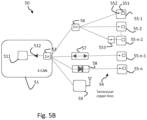
- Fig. 5B illustrates a schematic and extended layout (when compared to Fig. 5A ) of components of a communication system 50 to transmit data from one copper access node to several customer locations over twisted pairs using surface waves communication.
- the system as shown comprises as in Fig. 5A a surface-wave copper access node S-CAN 51.
- the S-CAN 51 is shown including a transceiver 511 and surface wave launcher 512 and integrates a splitter 53 or a cascade of such splitters forming a first 1:n splitter.
- the first surface wave splitter 53 in turn is connected on its CPE side to a further surface wave splitter 56 which connects to CPEs (Customer Premise Equipments) 55-1,..., 55-n-2 each with a transceiver 541 and a surface wave launcher 542 as already shown in Fig. 5A .
- CPEs Customer Premise Equipments
- the surface wave launcher is shown integrated into a separate wall plug 553. This particular set-up may have advantages as beyond the launcher the signal continues on the CPE side as normal wire-bound EM signal, i.e. as a LAN-type signal, not sensitive to attenuation through bending.
- the system 50 of Fig. 5B further includes example of a communication line including a surface wave repeater 57.
- the repeater is able to receive a signal with a launcher and launch it again. Such a unit is helpful in cases where the surface wave has less desired properties that yield higher attenuation than systems where the signal is transmitted in a cable. This are e.g. going around curves where the material on the inner side results in strong attenuation, window feed through, etc.
- the system 50 of Fig. 5B further includes example of a communication line including a surface wave amplifier 58.
- the amplifier may contain also an amplifier logic (for amplification in both up- and downlink) between the two launchers.
- 5B further includes example of a communication line including a surface wave wireless bridge 59, which can be applied to connect the surface wave system to a wireless system (not shown).
- the surface wave wireless bridge can be seen as a unit that translates the surface waves into a wireless signal that is sent over an antenna attached to the twisted pair cable.
- the surface wave wireless bridge may contain a filter (to select the desired frequency range) and a bi-directional amplifier (or two amplifiers for up- and downlink).
- the system may make use of a multiuser approach to mitigate crosstalk and other signal interferences between the signals of different users (CPEs). This can be done either by assigning different frequencies, different time-slots or different codes to a specific user, or any other multiple access scheme, for example.
Landscapes
- Engineering & Computer Science (AREA)
- Computer Networks & Wireless Communication (AREA)
- Signal Processing (AREA)
- Cable Transmission Systems, Equalization Of Radio And Reduction Of Echo (AREA)
Claims (8)
- Teiler, aufweisend ein Gehäuse, zur drahtgebundenen Oberflächenwellenkommunikation mit einer Vielzahl von E/A-Ports (RJ45(C0), RJ45(CPE)) zum Verbinden von externen Drähten, die Oberflächenwellen tragen, und aufweisend interne Drähte (41, 42, 42', 44a-44d'), die mindestens einen der Vielzahl von E/A-Ports durch den Innenraum des besagten Gehäuses mit mindestens zwei anderen der Vielzahl von E/A-Ports verbinden, um die Kommunikation von Oberflächenwellensignalen durch den Teiler zu ermöglichen, wobei die verbundenen E/A-Ports eine interne Ebene (101) innerhalb des Innenraums des Gehäuses des Teilers definieren und wobei sich einer oder mehrere der internen Drähte (41, 42, 42', 44a-44d') in das Volumen des Gehäuses über und/oder unter der internen Ebene (101) erstrecken.
- Teiler nach Anspruch 1, wobei nach einer ersten internen 1:2-Teiler-Stufe eines internen Oberflächenwellen tragenden Drahts (41), der mit dem mindestens einen der Vielzahl von E/A-Ports verbunden ist, sich die resultierenden zwei Drähte (42, 42') aus der internen Ebene (101) heraus erstrecken, sodass bei einer anschließenden 1:2-Teilung der resultierenden zwei Drähte (42, 42') sich die Stelle der besagten anschließenden Teilung ebenfalls außerhalb der internen Ebene (101) befindet, wobei jedoch nach einer letzten internen 1:2-Teiler-Stufe sich die Drähte (44a-44d'), die aus der letzten Teiler-Stufe resultieren, mit den mindestens zwei anderen der Vielzahl von E/A-Ports verbinden und somit die interne Ebene (101) abschließen.
- Teiler nach Anspruch 1 oder 2, wobei nach der ersten internen 1:2-Teiler-Stufe eines Drahts sich ein erster der zwei Drähte (42, 42') in das Volumen des Gehäuses über der internen Ebene (101) erstreckt und sich ein zweiter der zwei Drähte (42, 42') in das Volumen des Gehäuses unter der internen Ebene (101) erstreckt.
- Teiler nach einem der vorhergehenden Ansprüche, wobei der Biegewinkel jedes Drahts innerhalb des Gehäuses des Teilers bei einer beliebigen Biegung eines derartigen Drahts im Bereich von 0 bis 50 Grad, vorzugsweise 45 Grad liegt.
- Teiler nach einem der vorhergehenden Ansprüche, wobei der Biege- oder Krümmungsradius jedes Drahts innerhalbdes Gehäuses des Teilers bei einer beliebigen Biegung eines derartigen Drahts im Bereich von Unendlichkeit bis 3 mm, vorzugsweise 2,05 mm liegt.
- Teiler nach einem der vorhergehenden Ansprüche, wobei die Ports (RJ45(C0), RJ45(CPE)) des Teilers mit einem RJ45-Port pinkompatibel sind.
- Kommunikationsnetzwerk auf der Basis eines Austauschs von drahtgebundenen Oberflächenwellen zwischen einer Hauptniederlassungsstelle, CO-Stelle, und einer Teilnehmergerätestelle, CPE-Stelle, umfassend einen oder mehrere Teiler nach Anspruch 1 innerhalb des Netzwerks zwischen der Hauptniederlassungsstelle, CO-Stelle, und der Teilnehmergerätestelle, CPE-Stelle.
- Kommunikationsnetzwerk nach Anspruch 7, wobei der Teiler Oberflächenwellensignale gemäß einem CPE-spezifischen Signalmultiplex- oder -codierschema demultiplext/multiplext.
Priority Applications (1)
| Application Number | Priority Date | Filing Date | Title |
|---|---|---|---|
| EP19194711.8A EP3787104B1 (de) | 2019-08-30 | 2019-08-30 | Oberflächenwellenverteiler und netzwerkarchitektur |
Applications Claiming Priority (1)
| Application Number | Priority Date | Filing Date | Title |
|---|---|---|---|
| EP19194711.8A EP3787104B1 (de) | 2019-08-30 | 2019-08-30 | Oberflächenwellenverteiler und netzwerkarchitektur |
Publications (2)
| Publication Number | Publication Date |
|---|---|
| EP3787104A1 EP3787104A1 (de) | 2021-03-03 |
| EP3787104B1 true EP3787104B1 (de) | 2025-04-02 |
Family
ID=67840921
Family Applications (1)
| Application Number | Title | Priority Date | Filing Date |
|---|---|---|---|
| EP19194711.8A Active EP3787104B1 (de) | 2019-08-30 | 2019-08-30 | Oberflächenwellenverteiler und netzwerkarchitektur |
Country Status (1)
| Country | Link |
|---|---|
| EP (1) | EP3787104B1 (de) |
Citations (1)
| Publication number | Priority date | Publication date | Assignee | Title |
|---|---|---|---|---|
| US20120148052A1 (en) * | 2010-12-10 | 2012-06-14 | David Adam | System, Method, and Apparatus for Conveying a Signal to One or More Devices |
Family Cites Families (5)
| Publication number | Priority date | Publication date | Assignee | Title |
|---|---|---|---|---|
| JP2006099009A (ja) * | 2004-09-30 | 2006-04-13 | Sanyo Electric Co Ltd | 光分岐デバイス及び光カプラモジュール |
| KR101400128B1 (ko) * | 2013-01-25 | 2014-05-28 | 주식회사 대성정보통신기술 | 광 회선 분배기(ose) |
| US8897697B1 (en) | 2013-11-06 | 2014-11-25 | At&T Intellectual Property I, Lp | Millimeter-wave surface-wave communications |
| US9913139B2 (en) * | 2015-06-09 | 2018-03-06 | At&T Intellectual Property I, L.P. | Signal fingerprinting for authentication of communicating devices |
| US10256519B2 (en) * | 2016-12-30 | 2019-04-09 | Intel Corporation | Stranded transmission line and uses thereof |
-
2019
- 2019-08-30 EP EP19194711.8A patent/EP3787104B1/de active Active
Patent Citations (1)
| Publication number | Priority date | Publication date | Assignee | Title |
|---|---|---|---|---|
| US20120148052A1 (en) * | 2010-12-10 | 2012-06-14 | David Adam | System, Method, and Apparatus for Conveying a Signal to One or More Devices |
Also Published As
| Publication number | Publication date |
|---|---|
| EP3787104A1 (de) | 2021-03-03 |
Similar Documents
| Publication | Publication Date | Title |
|---|---|---|
| US11644619B2 (en) | Optical splitter chip, optical splitter component, optical splitter apparatus, and optical fiber box | |
| US7280011B2 (en) | Waveguide and method of manufacture | |
| CN104823092B (zh) | 具有中空伸缩波导的无线连接器 | |
| US20110311187A1 (en) | Hybrid 8p8c rj-45 modular plug configured with both optical and electrical connections for providing both optical and electrical communications capabilities, and a method | |
| JP6072011B2 (ja) | 統合型建物内ネットワーク | |
| EP3203287B1 (de) | Hybride mikrowellenkunststofffasern | |
| WO2001078435A2 (en) | Wireless communication methods and systems using multiple sectored cells | |
| US10305594B2 (en) | Wireless network cable assembly | |
| US5496196A (en) | CDDI connector for high-speed networks of voice and data transmissions | |
| EP2253981B1 (de) | Steckverbindergehäuse für ein Funk-über-Faser-Glasfaserkabelsystem | |
| EP3787104A1 (de) | Oberflächenwellenverteiler und netzwerkarchitektur | |
| EP0293419B1 (de) | Mit koppelstift versehene wellenleitermultiplexvorrichtung | |
| TW201944668A (zh) | 用於連接波導件和板件的連接器 | |
| US11041996B2 (en) | Wave conductor, waveguide connector, and communications link | |
| TWI655470B (zh) | 帶線式光通訊組件 | |
| KR101794986B1 (ko) | 멀티모드 광선로를 이용한 수동형 광가입자망 시스템 | |
| CN115425468B (zh) | 多点适配结构 | |
| CN116349085B (zh) | 用于对极化波进行复用或解复用的设备 | |
| US20260120921A1 (en) | Systems and methods providing optical cable with twisted copper pairs | |
| Bertran Albertí | Channel (regulations and physical) | |
| WO2020048131A1 (zh) | 耦合装置、表面波耦合方法及明线表面波无线覆盖系统 | |
| EP2598967A1 (de) | System mit einem modul | |
| GB2494264A (en) | A hybrid plug with electrical and optical connections | |
| CN108923212B (zh) | 一种线缆 | |
| US20230217582A1 (en) | Polymer microwave fiber transceiver |
Legal Events
| Date | Code | Title | Description |
|---|---|---|---|
| PUAI | Public reference made under article 153(3) epc to a published international application that has entered the european phase |
Free format text: ORIGINAL CODE: 0009012 |
|
| STAA | Information on the status of an ep patent application or granted ep patent |
Free format text: STATUS: THE APPLICATION HAS BEEN PUBLISHED |
|
| AK | Designated contracting states |
Kind code of ref document: A1 Designated state(s): AL AT BE BG CH CY CZ DE DK EE ES FI FR GB GR HR HU IE IS IT LI LT LU LV MC MK MT NL NO PL PT RO RS SE SI SK SM TR |
|
| AX | Request for extension of the european patent |
Extension state: BA ME |
|
| STAA | Information on the status of an ep patent application or granted ep patent |
Free format text: STATUS: REQUEST FOR EXAMINATION WAS MADE |
|
| 17P | Request for examination filed |
Effective date: 20210830 |
|
| RBV | Designated contracting states (corrected) |
Designated state(s): AL AT BE BG CH CY CZ DE DK EE ES FI FR GB GR HR HU IE IS IT LI LT LU LV MC MK MT NL NO PL PT RO RS SE SI SK SM TR |
|
| STAA | Information on the status of an ep patent application or granted ep patent |
Free format text: STATUS: EXAMINATION IS IN PROGRESS |
|
| 17Q | First examination report despatched |
Effective date: 20220920 |
|
| P01 | Opt-out of the competence of the unified patent court (upc) registered |
Effective date: 20230527 |
|
| RIC1 | Information provided on ipc code assigned before grant |
Ipc: H04B 3/32 20060101ALI20240321BHEP Ipc: H01P 5/12 20060101ALI20240321BHEP Ipc: H01P 3/10 20060101AFI20240321BHEP |
|
| GRAP | Despatch of communication of intention to grant a patent |
Free format text: ORIGINAL CODE: EPIDOSNIGR1 |
|
| STAA | Information on the status of an ep patent application or granted ep patent |
Free format text: STATUS: GRANT OF PATENT IS INTENDED |
|
| INTG | Intention to grant announced |
Effective date: 20240507 |
|
| GRAJ | Information related to disapproval of communication of intention to grant by the applicant or resumption of examination proceedings by the epo deleted |
Free format text: ORIGINAL CODE: EPIDOSDIGR1 |
|
| STAA | Information on the status of an ep patent application or granted ep patent |
Free format text: STATUS: EXAMINATION IS IN PROGRESS |
|
| INTC | Intention to grant announced (deleted) | ||
| GRAP | Despatch of communication of intention to grant a patent |
Free format text: ORIGINAL CODE: EPIDOSNIGR1 |
|
| STAA | Information on the status of an ep patent application or granted ep patent |
Free format text: STATUS: GRANT OF PATENT IS INTENDED |
|
| INTG | Intention to grant announced |
Effective date: 20241023 |
|
| GRAS | Grant fee paid |
Free format text: ORIGINAL CODE: EPIDOSNIGR3 |
|
| GRAA | (expected) grant |
Free format text: ORIGINAL CODE: 0009210 |
|
| STAA | Information on the status of an ep patent application or granted ep patent |
Free format text: STATUS: THE PATENT HAS BEEN GRANTED |
|
| AK | Designated contracting states |
Kind code of ref document: B1 Designated state(s): AL AT BE BG CH CY CZ DE DK EE ES FI FR GB GR HR HU IE IS IT LI LT LU LV MC MK MT NL NO PL PT RO RS SE SI SK SM TR |
|
| REG | Reference to a national code |
Ref country code: GB Ref legal event code: FG4D |
|
| REG | Reference to a national code |
Ref country code: CH Ref legal event code: EP |
|
| REG | Reference to a national code |
Ref country code: DE Ref legal event code: R096 Ref document number: 602019068019 Country of ref document: DE |
|
| REG | Reference to a national code |
Ref country code: IE Ref legal event code: FG4D |
|
| REG | Reference to a national code |
Ref country code: NL Ref legal event code: FP |
|
| PGFP | Annual fee paid to national office [announced via postgrant information from national office to epo] |
Ref country code: NL Payment date: 20250821 Year of fee payment: 7 |
|
| REG | Reference to a national code |
Ref country code: AT Ref legal event code: MK05 Ref document number: 1782245 Country of ref document: AT Kind code of ref document: T Effective date: 20250402 |
|
| PG25 | Lapsed in a contracting state [announced via postgrant information from national office to epo] |
Ref country code: FI Free format text: LAPSE BECAUSE OF FAILURE TO SUBMIT A TRANSLATION OF THE DESCRIPTION OR TO PAY THE FEE WITHIN THE PRESCRIBED TIME-LIMIT Effective date: 20250402 Ref country code: PT Free format text: LAPSE BECAUSE OF FAILURE TO SUBMIT A TRANSLATION OF THE DESCRIPTION OR TO PAY THE FEE WITHIN THE PRESCRIBED TIME-LIMIT Effective date: 20250804 Ref country code: ES Free format text: LAPSE BECAUSE OF FAILURE TO SUBMIT A TRANSLATION OF THE DESCRIPTION OR TO PAY THE FEE WITHIN THE PRESCRIBED TIME-LIMIT Effective date: 20250402 |
|
| PGFP | Annual fee paid to national office [announced via postgrant information from national office to epo] |
Ref country code: DE Payment date: 20250820 Year of fee payment: 7 |
|
| REG | Reference to a national code |
Ref country code: LT Ref legal event code: MG9D |
|
| PG25 | Lapsed in a contracting state [announced via postgrant information from national office to epo] |
Ref country code: GR Free format text: LAPSE BECAUSE OF FAILURE TO SUBMIT A TRANSLATION OF THE DESCRIPTION OR TO PAY THE FEE WITHIN THE PRESCRIBED TIME-LIMIT Effective date: 20250703 Ref country code: NO Free format text: LAPSE BECAUSE OF FAILURE TO SUBMIT A TRANSLATION OF THE DESCRIPTION OR TO PAY THE FEE WITHIN THE PRESCRIBED TIME-LIMIT Effective date: 20250702 |
|
| PG25 | Lapsed in a contracting state [announced via postgrant information from national office to epo] |
Ref country code: PL Free format text: LAPSE BECAUSE OF FAILURE TO SUBMIT A TRANSLATION OF THE DESCRIPTION OR TO PAY THE FEE WITHIN THE PRESCRIBED TIME-LIMIT Effective date: 20250402 |
|
| PG25 | Lapsed in a contracting state [announced via postgrant information from national office to epo] |
Ref country code: BG Free format text: LAPSE BECAUSE OF FAILURE TO SUBMIT A TRANSLATION OF THE DESCRIPTION OR TO PAY THE FEE WITHIN THE PRESCRIBED TIME-LIMIT Effective date: 20250402 |
|
| PGFP | Annual fee paid to national office [announced via postgrant information from national office to epo] |
Ref country code: GB Payment date: 20250820 Year of fee payment: 7 |
|
| PG25 | Lapsed in a contracting state [announced via postgrant information from national office to epo] |
Ref country code: HR Free format text: LAPSE BECAUSE OF FAILURE TO SUBMIT A TRANSLATION OF THE DESCRIPTION OR TO PAY THE FEE WITHIN THE PRESCRIBED TIME-LIMIT Effective date: 20250402 |
|
| PG25 | Lapsed in a contracting state [announced via postgrant information from national office to epo] |
Ref country code: AT Free format text: LAPSE BECAUSE OF FAILURE TO SUBMIT A TRANSLATION OF THE DESCRIPTION OR TO PAY THE FEE WITHIN THE PRESCRIBED TIME-LIMIT Effective date: 20250402 |
|
| PGFP | Annual fee paid to national office [announced via postgrant information from national office to epo] |
Ref country code: FR Payment date: 20250828 Year of fee payment: 7 |
|
| PGFP | Annual fee paid to national office [announced via postgrant information from national office to epo] |
Ref country code: CH Payment date: 20250901 Year of fee payment: 7 |
|
| PG25 | Lapsed in a contracting state [announced via postgrant information from national office to epo] |
Ref country code: RS Free format text: LAPSE BECAUSE OF FAILURE TO SUBMIT A TRANSLATION OF THE DESCRIPTION OR TO PAY THE FEE WITHIN THE PRESCRIBED TIME-LIMIT Effective date: 20250702 |
|
| PG25 | Lapsed in a contracting state [announced via postgrant information from national office to epo] |
Ref country code: IS Free format text: LAPSE BECAUSE OF FAILURE TO SUBMIT A TRANSLATION OF THE DESCRIPTION OR TO PAY THE FEE WITHIN THE PRESCRIBED TIME-LIMIT Effective date: 20250802 |
|
| PG25 | Lapsed in a contracting state [announced via postgrant information from national office to epo] |
Ref country code: LV Free format text: LAPSE BECAUSE OF FAILURE TO SUBMIT A TRANSLATION OF THE DESCRIPTION OR TO PAY THE FEE WITHIN THE PRESCRIBED TIME-LIMIT Effective date: 20250402 |
|
| REG | Reference to a national code |
Ref country code: DE Ref legal event code: R097 Ref document number: 602019068019 Country of ref document: DE |
|
| PG25 | Lapsed in a contracting state [announced via postgrant information from national office to epo] |
Ref country code: DK Free format text: LAPSE BECAUSE OF FAILURE TO SUBMIT A TRANSLATION OF THE DESCRIPTION OR TO PAY THE FEE WITHIN THE PRESCRIBED TIME-LIMIT Effective date: 20250402 Ref country code: SM Free format text: LAPSE BECAUSE OF FAILURE TO SUBMIT A TRANSLATION OF THE DESCRIPTION OR TO PAY THE FEE WITHIN THE PRESCRIBED TIME-LIMIT Effective date: 20250402 |
|
| PG25 | Lapsed in a contracting state [announced via postgrant information from national office to epo] |
Ref country code: CZ Free format text: LAPSE BECAUSE OF FAILURE TO SUBMIT A TRANSLATION OF THE DESCRIPTION OR TO PAY THE FEE WITHIN THE PRESCRIBED TIME-LIMIT Effective date: 20250402 |
|
| PG25 | Lapsed in a contracting state [announced via postgrant information from national office to epo] |
Ref country code: EE Free format text: LAPSE BECAUSE OF FAILURE TO SUBMIT A TRANSLATION OF THE DESCRIPTION OR TO PAY THE FEE WITHIN THE PRESCRIBED TIME-LIMIT Effective date: 20250402 |
|
| PG25 | Lapsed in a contracting state [announced via postgrant information from national office to epo] |
Ref country code: RO Free format text: LAPSE BECAUSE OF FAILURE TO SUBMIT A TRANSLATION OF THE DESCRIPTION OR TO PAY THE FEE WITHIN THE PRESCRIBED TIME-LIMIT Effective date: 20250402 Ref country code: SK Free format text: LAPSE BECAUSE OF FAILURE TO SUBMIT A TRANSLATION OF THE DESCRIPTION OR TO PAY THE FEE WITHIN THE PRESCRIBED TIME-LIMIT Effective date: 20250402 |
|
| PG25 | Lapsed in a contracting state [announced via postgrant information from national office to epo] |
Ref country code: IT Free format text: LAPSE BECAUSE OF FAILURE TO SUBMIT A TRANSLATION OF THE DESCRIPTION OR TO PAY THE FEE WITHIN THE PRESCRIBED TIME-LIMIT Effective date: 20250402 |
|
| PLBE | No opposition filed within time limit |
Free format text: ORIGINAL CODE: 0009261 |
|
| STAA | Information on the status of an ep patent application or granted ep patent |
Free format text: STATUS: NO OPPOSITION FILED WITHIN TIME LIMIT |
|
| REG | Reference to a national code |
Ref country code: CH Ref legal event code: L10 Free format text: ST27 STATUS EVENT CODE: U-0-0-L10-L00 (AS PROVIDED BY THE NATIONAL OFFICE) Effective date: 20260211 |
|
| 26N | No opposition filed |
Effective date: 20260105 |
|
| PG25 | Lapsed in a contracting state [announced via postgrant information from national office to epo] |
Ref country code: MC Free format text: LAPSE BECAUSE OF FAILURE TO SUBMIT A TRANSLATION OF THE DESCRIPTION OR TO PAY THE FEE WITHIN THE PRESCRIBED TIME-LIMIT Effective date: 20250402 |
|
| PG25 | Lapsed in a contracting state [announced via postgrant information from national office to epo] |
Ref country code: LU Free format text: LAPSE BECAUSE OF NON-PAYMENT OF DUE FEES Effective date: 20250830 |