EP3787023A1 - Imaging unit and method for manufacturing same - Google Patents
Imaging unit and method for manufacturing same Download PDFInfo
- Publication number
- EP3787023A1 EP3787023A1 EP19793883.0A EP19793883A EP3787023A1 EP 3787023 A1 EP3787023 A1 EP 3787023A1 EP 19793883 A EP19793883 A EP 19793883A EP 3787023 A1 EP3787023 A1 EP 3787023A1
- Authority
- EP
- European Patent Office
- Prior art keywords
- area
- semiconductor chip
- image capturing
- capturing unit
- substrate
- Prior art date
- Legal status (The legal status is an assumption and is not a legal conclusion. Google has not performed a legal analysis and makes no representation as to the accuracy of the status listed.)
- Granted
Links
Images






Classifications
-
- H—ELECTRICITY
- H10—SEMICONDUCTOR DEVICES; ELECTRIC SOLID-STATE DEVICES NOT OTHERWISE PROVIDED FOR
- H10F—INORGANIC SEMICONDUCTOR DEVICES SENSITIVE TO INFRARED RADIATION, LIGHT, ELECTROMAGNETIC RADIATION OF SHORTER WAVELENGTH OR CORPUSCULAR RADIATION
- H10F39/00—Integrated devices, or assemblies of multiple devices, comprising at least one element covered by group H10F30/00, e.g. radiation detectors comprising photodiode arrays
- H10F39/80—Constructional details of image sensors
- H10F39/811—Interconnections
-
- H—ELECTRICITY
- H10—SEMICONDUCTOR DEVICES; ELECTRIC SOLID-STATE DEVICES NOT OTHERWISE PROVIDED FOR
- H10W—GENERIC PACKAGES, INTERCONNECTIONS, CONNECTORS OR OTHER CONSTRUCTIONAL DETAILS OF DEVICES COVERED BY CLASS H10
- H10W90/00—Package configurations
-
- H—ELECTRICITY
- H10—SEMICONDUCTOR DEVICES; ELECTRIC SOLID-STATE DEVICES NOT OTHERWISE PROVIDED FOR
- H10F—INORGANIC SEMICONDUCTOR DEVICES SENSITIVE TO INFRARED RADIATION, LIGHT, ELECTROMAGNETIC RADIATION OF SHORTER WAVELENGTH OR CORPUSCULAR RADIATION
- H10F39/00—Integrated devices, or assemblies of multiple devices, comprising at least one element covered by group H10F30/00, e.g. radiation detectors comprising photodiode arrays
- H10F39/011—Manufacture or treatment of image sensors covered by group H10F39/12
-
- H—ELECTRICITY
- H10—SEMICONDUCTOR DEVICES; ELECTRIC SOLID-STATE DEVICES NOT OTHERWISE PROVIDED FOR
- H10F—INORGANIC SEMICONDUCTOR DEVICES SENSITIVE TO INFRARED RADIATION, LIGHT, ELECTROMAGNETIC RADIATION OF SHORTER WAVELENGTH OR CORPUSCULAR RADIATION
- H10F39/00—Integrated devices, or assemblies of multiple devices, comprising at least one element covered by group H10F30/00, e.g. radiation detectors comprising photodiode arrays
- H10F39/80—Constructional details of image sensors
- H10F39/802—Geometry or disposition of elements in pixels, e.g. address-lines or gate electrodes
-
- H—ELECTRICITY
- H10—SEMICONDUCTOR DEVICES; ELECTRIC SOLID-STATE DEVICES NOT OTHERWISE PROVIDED FOR
- H10F—INORGANIC SEMICONDUCTOR DEVICES SENSITIVE TO INFRARED RADIATION, LIGHT, ELECTROMAGNETIC RADIATION OF SHORTER WAVELENGTH OR CORPUSCULAR RADIATION
- H10F39/00—Integrated devices, or assemblies of multiple devices, comprising at least one element covered by group H10F30/00, e.g. radiation detectors comprising photodiode arrays
- H10F39/80—Constructional details of image sensors
- H10F39/804—Containers or encapsulations
-
- H—ELECTRICITY
- H05—ELECTRIC TECHNIQUES NOT OTHERWISE PROVIDED FOR
- H05K—PRINTED CIRCUITS; CASINGS OR CONSTRUCTIONAL DETAILS OF ELECTRIC APPARATUS; MANUFACTURE OF ASSEMBLAGES OF ELECTRICAL COMPONENTS
- H05K1/00—Printed circuits
- H05K1/18—Printed circuits structurally associated with non-printed electric components
- H05K1/181—Printed circuits structurally associated with non-printed electric components associated with surface mounted components
-
- H—ELECTRICITY
- H05—ELECTRIC TECHNIQUES NOT OTHERWISE PROVIDED FOR
- H05K—PRINTED CIRCUITS; CASINGS OR CONSTRUCTIONAL DETAILS OF ELECTRIC APPARATUS; MANUFACTURE OF ASSEMBLAGES OF ELECTRICAL COMPONENTS
- H05K2201/00—Indexing scheme relating to printed circuits covered by H05K1/00
- H05K2201/10—Details of components or other objects attached to or integrated in a printed circuit board
- H05K2201/10007—Types of components
- H05K2201/10151—Sensor
-
- H—ELECTRICITY
- H10—SEMICONDUCTOR DEVICES; ELECTRIC SOLID-STATE DEVICES NOT OTHERWISE PROVIDED FOR
- H10W—GENERIC PACKAGES, INTERCONNECTIONS, CONNECTORS OR OTHER CONSTRUCTIONAL DETAILS OF DEVICES COVERED BY CLASS H10
- H10W72/00—Interconnections or connectors in packages
- H10W72/071—Connecting or disconnecting
- H10W72/073—Connecting or disconnecting of die-attach connectors
-
- H—ELECTRICITY
- H10—SEMICONDUCTOR DEVICES; ELECTRIC SOLID-STATE DEVICES NOT OTHERWISE PROVIDED FOR
- H10W—GENERIC PACKAGES, INTERCONNECTIONS, CONNECTORS OR OTHER CONSTRUCTIONAL DETAILS OF DEVICES COVERED BY CLASS H10
- H10W72/00—Interconnections or connectors in packages
- H10W72/071—Connecting or disconnecting
- H10W72/075—Connecting or disconnecting of bond wires
-
- H—ELECTRICITY
- H10—SEMICONDUCTOR DEVICES; ELECTRIC SOLID-STATE DEVICES NOT OTHERWISE PROVIDED FOR
- H10W—GENERIC PACKAGES, INTERCONNECTIONS, CONNECTORS OR OTHER CONSTRUCTIONAL DETAILS OF DEVICES COVERED BY CLASS H10
- H10W72/00—Interconnections or connectors in packages
- H10W72/50—Bond wires
- H10W72/551—Materials of bond wires
- H10W72/552—Materials of bond wires comprising metals or metalloids, e.g. silver
- H10W72/5522—Materials of bond wires comprising metals or metalloids, e.g. silver comprising gold [Au]
-
- H—ELECTRICITY
- H10—SEMICONDUCTOR DEVICES; ELECTRIC SOLID-STATE DEVICES NOT OTHERWISE PROVIDED FOR
- H10W—GENERIC PACKAGES, INTERCONNECTIONS, CONNECTORS OR OTHER CONSTRUCTIONAL DETAILS OF DEVICES COVERED BY CLASS H10
- H10W72/00—Interconnections or connectors in packages
- H10W72/851—Dispositions of multiple connectors or interconnections
- H10W72/874—On different surfaces
- H10W72/884—Die-attach connectors and bond wires
-
- H—ELECTRICITY
- H10—SEMICONDUCTOR DEVICES; ELECTRIC SOLID-STATE DEVICES NOT OTHERWISE PROVIDED FOR
- H10W—GENERIC PACKAGES, INTERCONNECTIONS, CONNECTORS OR OTHER CONSTRUCTIONAL DETAILS OF DEVICES COVERED BY CLASS H10
- H10W90/00—Package configurations
- H10W90/701—Package configurations characterised by the relative positions of pads or connectors relative to package parts
- H10W90/751—Package configurations characterised by the relative positions of pads or connectors relative to package parts of bond wires
- H10W90/754—Package configurations characterised by the relative positions of pads or connectors relative to package parts of bond wires between a chip and a stacked insulating package substrate, interposer or RDL
Definitions
- the present invention relates to an image capturing unit using an image sensor.
- a sensor chip comprising a silicon substrate and others is mounted within a package formed of ceramic or plastic with a recessed cavity.
- a so-called packageless structure as disclosed in PTL 1 is proposed in which a sensor chip is mounted directly on a printed circuit board made of glass epoxy or the like.
- the packageless structure needs to heat the printed circuit board in connecting the sensor chip and the printed circuit board with wire bonding. This has a problem in that an area of the printed circuit board in which components can be disposed is decreased.
- An object of the present invention is to provide an image capturing unit with a packageless structure that allows an optimum inspection of the sensor chip in a manufacturing process and an inspection process without decreasing the signal quality.
- an image capturing unit is an image capturing unit including a semiconductor chip constituting an image sensor and a substrate on which the semiconductor chip is mounted.
- the image capturing unit is characterized by including a plurality of input wiring lines for controlling the semiconductor chip, a plurality of first electrodes connecting to the input wiring lines, and an input connector connecting to the input wiring lines.
- the substrate includes, in an opposite surface from a surface on which the semiconductor chip is mounted, a first area for mounting an electronic component and a second area for use in mounting the semiconductor chip.
- the connector is disposed in the first area. At least one or more of the first electrodes are disposed in the second area.
- the present invention provides an image capturing unit with a packageless structure that allows an optimum inspection of a sensor chip in a manufacturing process and an inspection process without decreasing the signal quality.
- FIG. 1 is a diagram illustrating, in outline, the configuration of an image capturing unit of an embodiment of the present invention.
- Reference sign 101 denotes a sensor chip that outputs an image signal according to incident light.
- the sensor chip 101 is a semiconductor chip, such as a complementary metal-oxide semiconductor (CMOS) image sensor, formed on a silicon substrate.
- CMOS complementary metal-oxide semiconductor
- the sensor chip 101 may be a charge-coupled device (CCD) sensor or an image sensor made of a semiconductor other than silicon.
- CCD charge-coupled device
- the present invention is suitable for the configuration of the sensor chip 101 including multiple input and output signal lines and is more suitable for laminated image sensors in which a signal processing chip for signal processing is laminated on an imaging chip including a photoelectric conversion unit that converts light to electricity.
- Reference sign 102 denotes an imaging substrate.
- the imaging substrate 102 is a printed circuit board, on which components 103 (described later) are disposed.
- the individual patterns on the imaging substrate 102 are made of metal with low electric resistance, such as gold and copper, and are electrically connected to the sensor chip 101 using wire bonding wiring or the like using gold wires or the like.
- the imaging substrate 102 is preferably a rigid substrate and is made of glass epoxy or the like in consideration of stability for mounting the sensor chip 101. However, this is not intended to limit the present invention.
- the imaging substrate 102 may be a flexible substrate made of a plastic material or a low-temperature co-fired ceramic (LTCC) substrate made of ceramic and copper wires.
- LTCC low-temperature co-fired ceramic
- the imaging substrate 102 may be any substrate in which patterns made of a metal wire, such as a copper wire, is formed on a specific material and on which the components can be mounted.
- the printed circuit board may be a substrate including a plurality of layers composed of different materials that are made conducting through vias or the like.
- Reference sign 103 denotes an electronic component.
- the electronic components 103 include discrete components, such as capacitors, resistors, and coils, necessary for operating the sensor chip 101.
- the electronic components 103 further include IC chips, such as regulators for supplying power for operating the sensor chip 101 and an oscillator that supplies a clock signal.
- the electronic components 103 may include other components not for use in operating the sensor chip 101, such as a thermometer that monitors the state of the sensor chip 101 and a memory that stores the solid-state information on the sensor chip 101.
- the electronic components 103 are generally mounted on the opposite surface of the imaging substrate 102 from the sensor chip 101. Alternatively, a capacitor for removing noise, and so on may be mounted on the same surface such as that of the sensor chip 101 because they are preferably close to connection terminals.
- Reference sign 104 denotes a connector including a plurality of electrical contacts.
- An example is a board-to-board (B-to-B) connector, which is a component for transferring power and signals between the imaging substrate 102 and an external substrate including a signal processing chip for processing captured signals obtained from the sensor chip 101, to which various signals are connected in a lump.
- the connector may be a connector for connecting a flexible substrate.
- the connector 104 is mounted on the opposite surface of the imaging substrate 102 from the sensor chip 101. If the number of terminals that need to be connected to the external substrate increases with an increase in the function of the sensor chip 101, the size of the connector 104 will also increase. In this case, a plurality of connectors 104 are preferably used to connect to the external substrate.
- the range on the imaging substrate 102 indicated by arrow 105 is an area that substantially coincides with the back of the sensor chip 101, indicating a component area in which the components 103 and the connector 104 are disposed.
- the range indicated by arrow 106 is an area around the component area 105, indicating a forbidden area in which the electronic components 103 and the connector 104 are not disposed.
- the imaging substrate 102 can be deformed due to heat or the like, and the electronic components 103 are preferably mounted not in the peripheral portion, which is significantly affected by the deformation, but in the vicinity of the back of the sensor chip 101.
- the component area 105 corresponds to the first area
- the forbidden area 106 corresponds to the second area. It is preferable to provide wire bonding pads 107 (described later) on the opposite surface from the area corresponding to the forbidden area 106.
- the component area 105 is larger than the back of the sensor chip 101. This is a configuration in the case where the components 103 for driving the sensor chip 101 are large in number or size.
- the component area 105 increases in size and is larger than the area in which the wire bonding pad 107 is disposed.
- the size of the component area 105 is not limited as long as the imaging substrate 102 can be hold in heating or manufacturing the wire bonding pad 107.
- the component area 105 and the forbidden area 106 are determined depending on the size of the sensor chip 101, the number of components 103, and so on.
- reference sign 107 denotes a wire bonding pad for connecting the sensor chip 101 and the imaging substrate 102 together by wire bonding with gold wires or the like.
- the wire bonding pad 107 is an electrode formed on the surface of the imaging substrate 102 by surface treatment, such as gold plating.
- the wire bonding pad 107 is disposed on the same surface of the imaging substrate 102 such as that of the sensor chip 101.
- Reference sign 108 denotes a check pad (hereinafter sometimes referred to as CP), which is an electrode formed on the surface layer of the imaging substrate 102, like the wire bonding pad 107, by, for example, gold, copper, aluminum, or solder plating.
- the CPs 108 are disposed on the same surface of the imaging substrate 102 such as that of the connector 104.
- the area on the imaging substrate 102 indicated by arrow 106 is a heating area to which a heater or the like is to be brought into contact to heat the wire bonding pads 107 in wire bonding.
- the area 106 is also used to fix and position the imaging substrate 102 in manufacturing the image capturing unit, in addition to heating the wire bonding pads 107.
- the forbidden area 106 needs only have an area necessary for a fixing holder or the like to come into contact.
- the outer shape of the imaging substrate 102 increases or the component area 105 for the components decreases as the area of the forbidden area 106 increases. For that reason, more specifically, the forbidden area 106 is preferably inside the outer periphery of the imaging substrate 102 by about 1 mm to 8 mm.
- the component area 105 is preferably the same area as the outer periphery of the sensor chip 101 or the outer periphery of the substrate inside the sensor chip 101 by about 0 mm to 5 mm.
- the forbidden area 106 is preferably disposed along the four sides of along the outer periphery of the imaging substrate 102, this is not essential.
- the forbidden area 106 may be disposed on one side or two sides along the outer periphery of the imaging substrate 102, and each areas can be of different sizes and/or shapes as long as the fixing holder can be brought into contact.
- Reference sign 109 denotes a cover glass for sealing the sensor chip 101.
- the cover glass 109 has an antireflection coat and an infrared cut coat.
- the cover glass 109 may have the effect of an optical low-pass filter.
- Reference sign 110 denotes a frame, which is formed around the outer periphery of the wire bonding pads 107.
- the frame 110 is bonded to the imaging substrate 102 and the cover glass 109 to seal the sensor chip 101.
- the sides of the frame 110 do not need to be perpendicular to the imaging substrate 102 and have a predetermined inclination to suppress the reflection of the sides.
- the frame 110 is formed of resin or the like but may be formed of a ceramic material, a metallic material, or combination thereof.
- the frame 110 may include a fixing unit made of metal or the like for fixing to the main body of the image capturing apparatus, described later.
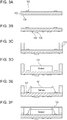
- FIG. 3 is a diagram illustrating, in outline, the manufacturing procedure of an image capturing unit of an embodiment of the present invention.
- FIG. 3A illustrates a state of only the imaging substrate 102, in which the components 103 and so on are not mounted.
- the assembly is performed, with the imaging substrate 102, which is a combination of a plurality of substrates, fixed to a predetermined jig, such as a tray (omitted in FIG. 3A ).
- the wire bonding pads 107 and the CPs 108 are formed on the imaging substrate 102, as described above. Patterns for mounting the components 103 and wires connecting the components are also formed (not illustrated).
- FIG. 3B illustrates a state in which the components 103 and the connector 104 are mounted on the imaging substrate 102.
- the components are mounted on the imaging substrate 102 by reflow soldering or the like in which it is coated with cream solder or the like using a predetermined mask.
- the wire bonding pads 107 may be surface-treated using a sputtering technique.
- FIG. 3C illustrates a state in which the frame 110 is bonded to the imaging substrate 102.
- the bonding is performed using a photo-curable resin or the like, but any other method can be used in the present invention.
- FIG. 3D illustrates a state in which the sensor chip 101 is mounted on the imaging substrate 102. The sensor chip 101 is fixed to the imaging substrate 102 with an adhesive (not illustrated).
- FIG. 3E illustrates a state in which the sensor chip 101 and the wire bonding pads 107 are bonded by wire bonding. In the wire bonding operation for connecting the sensor chip 101 and the imaging substrate 102, the sensor chip 101 and the imaging substrate 102 are heated on a heat stage to melt metal for use in wire bonding.
- FIG. 3F the sensor chip 101 is sealed with the cover glass 109, so that the image capturing unit is assembled.
- the image capturing unit in the present embodiment checks whether the image capturing unit manufactured in the manufacturing procedure illustrated in FIG. 3 can normally operate (generate electrically normal signals).
- the image capturing unit supplies power and clock to the sensor chip 101 and determines whether a predetermined signal is output (specifically described later). If an expected signal is output, the image capturing unit is determined to be a nondefective item, and if not, the image capturing unit is determined to be a defective item.
- the sensor chip 101 mounted in the image capturing unit of the present embodiment is inspected for operation also in a wafer state before assembling. The details of inspection in the wafer state is the same as the inspection of the image capturing unit, described later. In other words, the sensor chip 101 is inspected twice.
- the sensor chip 101 is heated during wire bonding and is brought into contact with various components during the assembly process, as described with reference to FIG. 3 , and in the sequence of operations, the sensor chip 101 can fail especially before being sealed with the cover glass 109. For this reason, it is necessary to check whether the image capturing unit normally operates after being assembled.
- An image capturing unit with a cavity structure is sealed with the cover glass 109 before being mounted on a printed circuit board to which multiple electronic components are mounted. This allows for pre-mounting inspection at the stage of a small package.
- the inspection is performed with the inclusion of the printed circuit board. In this case, not only the sensor chip 101 but also the imaging substrate 102 and the other electronic components are inspected. In some cases, the size of the image capturing unit is relatively large, which requires a simple configuration for inspection.
- FIGs. 4 to 6 a circuit block diagram for the CPs 108 for use in inspection and connection of the components will be described.
- FIG. 4 illustrates, in outline, the signal relationship of an image capturing unit according to an embodiment of the present invention.
- Reference sign 401 denotes an input connector of the connector 104.
- the input connector 401 is a connector for connecting to an external substrate including a control unit that controls the sensor chip 101 so that it captures images, to which signals for driving the sensor chip 101 are connected.
- the signals for driving the sensor chip 101 in the present embodiment include a clock signal, a synchronization signal, a serial communication signal, and a power source.
- the signals input from input connector 401 are input to the sensor chip 101 through input wiring lines 402 wired on the imaging substrate 102.
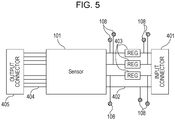
- Part of the power supply circuit for driving the sensor chip 101 can supply stable power to the sensor chip 101 using linear regulators 403 disposed in intermediate points of the wires 402.
- the linear regulators 403 are not absolutely necessary. Power may be directly supplied via the input connector 401.
- the number of signals connected to the input connector 401 is about ten.
- Reference sign 405 denotes an output connector of the connector 104.
- the output connector 405 is a connector for connecting to an external substrate including a signal processing unit for generating image data from an output signal from the sensor chip 101, to which serial signal lines and so on for outputting signals are connected.
- the output signals from the sensor chip 101 in the present embodiment include not only pixel signals from the pixels but also information on the output pixel signals (addresses, attributes, and so on of the pixels), a header or footer, synchronous code, and a clock signal for receiving image signals.
- the processing result may be output as output signals.
- the signals output to the output connector 405 are output from the sensor chip 101 through the output wiring lines 404 wired on the imaging substrate 102. Since the signals from the sensor chip 101 require high-speed transmission, the output wiring lines 404 are differential serial signal lines conforming to the low-voltage differential signaling (LVDS) standard or the scalable low-voltage signaling (SLVS) standard. The number of output channels from the sensor chip 101 is 20, and 40 signal lines are wired at equal length on the imaging substrate 102.
- LVDS low-voltage differential signaling
- SLVS scalable low-voltage signaling
- the CPs 108 are connected to the corresponding input wiring lines 402 between the input connector 401 and the sensor chip 101 via predetermined wires.
- the sensor chip 101 can be driven via the CPs 108 without connecting the input connector to an external substrate including a control unit.
- the CPs 108 are mainly used to execute electrical inspection of the sensor chip 101 without using the input connector 401 in inspecting the image capturing unit.
- the CPs 108 are connected also in the wiring lines between the linear regulators 403 and the sensor chip 101.
- This configuration allows for inputting inspection voltages other than the voltages generated by the linear regulators 403 to the sensor chip 101. Since the linear regulators 403 are components for supplying voltages for the normal operation of the sensor chip 101, this configuration is needed for inspection using another voltage. For example, by applying a high voltage or a low voltage, the sensor chip 101 can be operated in an inspection drive mode, or by applying a reverse bias, inspection in an abnormal state can be performed.
- switches 601 which are switch circuits, are disposed between the linear regulators 403 and the sensor chip 101.
- This configuration allows for applying various voltages from the outside via the CPs 108 between the sensor chip 101 and the switches 601.
- the power applied from the outside to the linear regulators 403 via the switches 601 can be separated. This allows the voltage to be applied to the sensor chip 101 via the CPs 108 to be set in a wide range without being limited by the power-supply voltages of the linear regulators 403 or the like.
- Signals and power for controlling the switches 601 can be provided by being input via the CPs 108 likewise.
- FIG. 7 illustrates, in outline, the connection relationship in the inspection and the usage of an image capturing unit of an embodiment of the present invention.
- FIG. 7A is a diagram illustrating the connection relationship in the inspection of the image capturing unit.
- Reference sign 701 denotes an interface substrate of an inspection apparatus. The image capturing unit is attached to the substrate for inspection. The interface substrate 701 supplies signals for driving the sensor chip 101 via the CPs 108 and receives output signals via the output connector 405.
- Reference sign 702 denotes an inspection connector, which is connected to the output connector 405. General B-to-B connectors perform holding to prevent dropping after being combined.
- the interface substrate 701 includes dedicated non-holding components to repeatedly attach and detach a plurality of image capturing units.
- Reference sign 703 denotes an inspection pin, which is connected to the CP 108 when the image capturing unit is attached to the interface substrate 701. The inspection pin 703 is an extendable contact, which can establish electrical conduction by being pushed against the CP 108. The inspection pin 703 is used to supply a signal and power for driving the sensor chip 101.
- FIG. 7B is a diagram illustrating the connection relationship of the image capturing unit in normal use.
- "In normal use” indicates a case in which the image capturing unit is installed in an image capturing apparatus (described later) and is used in an operation for capturing a subject image through a lens.
- Reference sign 704 denotes a first connector to be connected to the output connector 405, and reference sign 705 denotes a second connector to be connected to the input connector.
- the image capturing unit is connected to another substrate via the first connector 704 and the second connector 705.
- the first connector 704 and the second connector 705 are mounted on different substrates (not illustrated).
- the input connector 401 and the output connector 405 are precise electronic components but certainly have dimensional errors in mass production. Furthermore, adding the accuracy of mounting to the imaging substrate 102, the accuracy of the flatness of the imaging substrate 102 itself, and so on may cause the dimensions to deviate from a dimensional range for normal engagement. For these reasons, mounting the first connector 704 and the second connector 705 on the same substrate would not ensure normal engagement because of their tolerances. To prevent it, the first connector 704 and the second connector 705 are preferably disposed on different substrates and are individually connected. Alternatively, the same substrate may be used, as long as it is a flexible substrate that can accommodate the tolerances.
- the image capturing unit is attached to the inspection apparatus using an automatic transfer machine or the like in consideration of adhesion of dust and an electrostatic discharge failure.
- the connectors are preferably disposed on a single substrate. However, this may not ensure the engagement of the connectors, as described above. Disposing the connectors on different substrates or a flexible substrate will require a mounting transfer machine with a complicated structure and increase the inspection time. In other words, when a plurality of image capturing units are to be inspected using one inspection apparatus, two connectors cannot be used, decreasing the productivity.
- FIGs. 8 to 11 are diagrams illustrating, in outline, the layout of an imaging substrate of an embodiment of the present invention.
- FIG. 8A illustrates the layout of the surface (front) of the imaging substrate 102 on which the sensor chip 101 is mounted.
- FIG. 8B illustrates the layout of the surface (back) of the imaging substrate 102 on which the components 103 are disposed.
- Reference sign 801 denotes an area in which the sensor chip 101 is disposed.
- the wire bonding pads 107 are disposed around the sensor chip 101.
- the input connector 401, the output connector 405, the components 103, and so on are disposed in the component area 105.
- the area 106 is outside the component area 105 and extends to the end of the imaging substrate 102.
- the image-sensor area 801 is illustrated also in the layout of the back of the substrate on which the components 103 are disposed for simplicity sake.
- the sensor chip area 801 is not actually present on the front of the substrate on which the components are disposed.
- the component area 105 is described as an area smaller than the sensor chip 101, as illustrated in FIG. 1 , the present invention is not limited to this configuration.
- the CPs 108 are disposed in the area 106, as described above.
- the CPs 108 are most preferably disposed on one or more sides depending on the number of CPs 108. Disposing the CPs 108 on the long side of the image sensor rather than the short side can increase the area for the CPs 108.
- FIG. 9 illustrates another example of the arrangement of the CPs 108, in which the CPs 108 are disposed on the side symmetric about the direction in which the output connector 405 is disposed.
- the arrangement illustrated in FIG. 9 allows the pressure applied to the imaging substrate 102 when the inspection connector 702 and the inspection pins 703 are pushed against the image capturing unit at the inspection described above to be made uniform. The uniform pressure prevents the components from being damaged and increases the stability to conduction of the contacts.
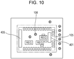
- FIG. 10 illustrates another example of the arrangement of the CPs 108, some of which are disposed also in the component area 105.
- the CPs 108 in the case of the wiring in FIG. 5 or FIG. 6 , it may be preferable to dispose the CPs 108 near the output of the linear regulators in terms of performance.
- the CPs 108 is preferably disposed in the component area 105.
- disposing the CPs 108 in the component area will decrease the area of the component area 105 for the components 103.
- the number of CPs 108 in the area 106 is preferably larger than the number of CPs in the area 105.
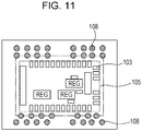
- FIG. 11 illustrates another example of the arrangement of the CPs 108, illustrating a case in which the CPs 108 are arranged in multiple rows and a case in which they are arranged in a staggered pattern.
- disposing multiple rows of CPs 108 are arranged, as in the drawing, can increase the area of the area 106 and decrease the area of the component area 105, which is advantageous when the area 106 is sufficiently large.
- Disposing many of the CPs 108 in the area 106 allows for not only suitably disposing the component area 105 but also providing the area 106 on the periphery of the substrate. This also contributes to the stability to conduction during inspection. This also allows for suitably supporting the substrate in heating during wire bonding and manufacturing.
- Disposing the CPs 108 not for the output connector 405 through which high-speed signal lines pass but only for input signals allows for inspection in the case of two connectors and allows inspection without decreasing the output signal quality. This also allows for supplying a voltage necessary for inspection to the sensor chip 101 without being influenced by the voltages of the linear regulators.
- FIG. 12 an embodiment in which the image sensor described in the above embodiments is applied to a digital camera, which is an image capturing apparatus, will be described in detail.
- reference sign 1201 denotes a lens unit that forms an optical image of the subject on the sensor chip 101, of which zoom control, focus control, aperture control and so on are performed by a lens driving unit 1202.
- Reference sign 1203 denotes a mechanical shutter, which is controlled by a shutter control unit 1204.
- Reference sign 101 denotes an image sensor for receiving an image of the subject formed by the lens unit 1201 as an image signal.
- Reference sign 1206 denotes a captured-signal processing circuit that performs various corrections on the image signal output from the solid-state image sensor 1205 or compresses data.
- Reference sign 1207 denotes a timing generation circuit which is a driving unit that outputs various timing signals to the sensor chip 101 and the captured-signal processing circuit 1206, reference sign 1209 denotes a control circuit that performs various kinds of calculation and controls the entire image capturing apparatus, and reference sign 1208 denotes a memory for temporarily storing image data.
- Reference sign 1210 denotes an interface for recording or reading to or from a recording medium
- 1211 denotes a detachable recording medium, such as a semiconductor memory, for recording or reading image data
- 1212 denotes a display that displays various pieces of information and captured images.
- Reference sign 1213 denotes a metering unit that detects the luminance of the subject.
- Reference sign 1214 denotes a distance measuring unit that detects a focus.
- the sensor chip 101 is mounted on the imaging substrate 102, and the imaging substrate 102 is connected to a substrate on which the captured-signal processing circuit 1206 and the timing generation unit 1207 are mounted via the connector.
- the power source of the control system When the main power source is turned on, the power source of the control system is turned on, and the power source of the image capturing circuit, such as the captured-signal processing circuit 1206, is turned on.
- a release button (not illustrate) is pressed, a high-frequency component is taken out on the basis of a signal output from the distance measuring unit 1214 to calculate the distance to the subject with the control circuit 1209. Thereafter, the lens unit is driven by the lens driving unit 1202, and it is determined whether the subject is in focus. If it is determined that the subject is not in focus, the lens unit is driven again, and distance measurement is performed.
- an image signal output from the sensor chip 101 is processed by the captured-signal processing circuit 1206, and the signal is written to the memory 1208 by the control circuit 1209.
- the data accumulated in the memory 1208 is recorded in the detachable recording medium 1211, such as a semiconductor memory, via the recording-medium control I/F 1210 under the control of the control circuit 1209.
- the image may be directly input to a computer or the like via an external I/F 1210 for processing.
- the image capturing units and image capturing apparatuses described in the embodiments are applicable to various applications.
- the image capturing units can be used in sensing not only visible light but also infrared light, ultraviolet light, X-rays, and other light.
- the image capturing apparatuses are typified by digital camera but may be used for mobile phones with a camera, such as smartphones, monitoring cameras, and game machines.
- the image capturing apparatuses can also be used for endoscopes, angiographic medical devices, cosmetic devices for observing skin or scalps, and video cameras for capturing sports and action moving images.
- the image capturing apparatuses can also be used for traffic cameras for traffic or vessel monitoring, such as drive recorders, academic-application cameras for astronomical observation or analyte observation, home electric appliances with camera, machine vision, and so on.
- traffic cameras for traffic or vessel monitoring
- the machine vision is applicable not only in robots in factories or the like but also in agriculture and fishery.
- the configurations of the image capturing apparatuses in the above embodiments are mere examples, and the configurations of the image capturing apparatuses to which the present invention can be applied are not limited to the configuration illustrated in FIG. 1 .
- the circuit configurations of the components of the image capturing apparatuses are not limited to the configurations illustrated in the drawings.
- the present invention can be implemented by processing of supplying a program for implementing one or more functions of the above-described embodiments to a system or apparatus via a network or storage medium, and causing one or more processors in the computer of the system or apparatus to read out and execute the program.
- the present invention can also be implemented by a circuit (for example, an ASIC) for implementing one or more functions.
Landscapes
- Solid State Image Pick-Up Elements (AREA)
- Camera Bodies And Camera Details Or Accessories (AREA)
- Structures For Mounting Electric Components On Printed Circuit Boards (AREA)
- Wire Bonding (AREA)
Abstract
Description
- The present invention relates to an image capturing unit using an image sensor.
- In general structure of known image sensors used in digital cameras, a sensor chip comprising a silicon substrate and others is mounted within a package formed of ceramic or plastic with a recessed cavity. However, as packages have decreased in weight and size, a so-called packageless structure as disclosed in PTL 1 is proposed in which a sensor chip is mounted directly on a printed circuit board made of glass epoxy or the like.
- PTL 1: Japanese Patent Laid-Open No.
2015-012211 - However, as disclosed in PTL 1, the packageless structure needs to heat the printed circuit board in connecting the sensor chip and the printed circuit board with wire bonding. This has a problem in that an area of the printed circuit board in which components can be disposed is decreased.
- Furthermore, an electrical inspection is needed after the sensor chip is mounted. This requires an additional terminal for inspection on the printed circuit board, causing the problem of increasing the board size. Furthermore, providing the terminal for inspection to output lines operating at high-speed clock will add a stub to the output line, and thus may degrade the quality of the output signal.
- An object of the present invention is to provide an image capturing unit with a packageless structure that allows an optimum inspection of the sensor chip in a manufacturing process and an inspection process without decreasing the signal quality.
- To achieve the above object, an image capturing unit according to the present invention is an image capturing unit including a semiconductor chip constituting an image sensor and a substrate on which the semiconductor chip is mounted. The image capturing unit is characterized by including a plurality of input wiring lines for controlling the semiconductor chip, a plurality of first electrodes connecting to the input wiring lines, and an input connector connecting to the input wiring lines. The substrate includes, in an opposite surface from a surface on which the semiconductor chip is mounted, a first area for mounting an electronic component and a second area for use in mounting the semiconductor chip. The connector is disposed in the first area. At least one or more of the first electrodes are disposed in the second area.
- The present invention provides an image capturing unit with a packageless structure that allows an optimum inspection of a sensor chip in a manufacturing process and an inspection process without decreasing the signal quality.
-
-
FIG. 1 is a diagram illustrating the configuration of an image capturing unit according to an embodiment of the present invention. -
FIG. 2A is a diagram illustrating another configuration of the image capturing unit according to the embodiment of the present invention. -
FIG. 2B is a diagram illustrating another configuration of the image capturing unit according to the embodiment of the present invention. -
FIG. 3A is a diagram illustrating the manufacturing procedure of the image capturing unit according to the embodiment of the present invention. -
FIG. 3B is a diagram illustrating the manufacturing procedure of the image capturing unit according to the embodiment of the present invention. -
FIG. 3C is a diagram illustrating the manufacturing procedure of the image capturing unit according to the embodiment of the present invention. -
FIG. 3D is a diagram illustrating the manufacturing procedure of the image capturing unit according to the embodiment of the present invention. -
FIG. 3E is a diagram illustrating the manufacturing procedure of the image capturing unit according to the embodiment of the present invention. -
FIG. 3F is a diagram illustrating the manufacturing procedure of the image capturing unit according to the embodiment of the present invention. -
FIG. 4 is a block diagram of an image capturing unit according to an embodiment of the present invention. -
FIG. 5 is another block diagram of an image capturing unit according to an embodiment of the present invention. -
FIG. 6 is another block diagram of an image capturing unit according to an embodiment of the present invention. -
FIG. 7A is a diagram illustrating the configuration of connection to an image capturing unit of an embodiment of the present invention. -
FIG. 7B is a diagram illustrating the configuration of connection to an image capturing unit of an embodiment of the present invention. -
FIG. 8A is a diagram illustrating the layout of an imaging substrate according to an embodiment of the present invention. -
FIG. 8B is a diagram illustrating the layout of the imaging substrate according to the embodiment of the present invention. -
FIG. 9 is a diagram illustrating another layout of an imaging substrate according to an embodiment of the present invention. -
FIG. 10 is a diagram illustrating another layout of an imaging substrate according to an embodiment of the present invention. -
FIG. 11 is a diagram illustrating another layout of an imaging substrate according to an embodiment of the present invention. -
FIG. 12 is a block diagram of an image capturing apparatus according to an embodiment of the present invention. - Embodiments of the present invention will be described hereinbelow with reference to the drawings. In all of the drawings, components having the same function are denoted by the same reference sign, and a repeated description thereof will be omitted. The components are not limited to the details of the embodiments and can be corrected as appropriate.
-
FIG. 1 is a diagram illustrating, in outline, the configuration of an image capturing unit of an embodiment of the present invention. -
Reference sign 101 denotes a sensor chip that outputs an image signal according to incident light. In the present embodiment, thesensor chip 101 is a semiconductor chip, such as a complementary metal-oxide semiconductor (CMOS) image sensor, formed on a silicon substrate. Alternatively, thesensor chip 101 may be a charge-coupled device (CCD) sensor or an image sensor made of a semiconductor other than silicon. The present invention is suitable for the configuration of thesensor chip 101 including multiple input and output signal lines and is more suitable for laminated image sensors in which a signal processing chip for signal processing is laminated on an imaging chip including a photoelectric conversion unit that converts light to electricity. -
Reference sign 102 denotes an imaging substrate. In the present embodiment, theimaging substrate 102 is a printed circuit board, on which components 103 (described later) are disposed. The individual patterns on theimaging substrate 102 are made of metal with low electric resistance, such as gold and copper, and are electrically connected to thesensor chip 101 using wire bonding wiring or the like using gold wires or the like. Theimaging substrate 102 is preferably a rigid substrate and is made of glass epoxy or the like in consideration of stability for mounting thesensor chip 101. However, this is not intended to limit the present invention. Theimaging substrate 102 may be a flexible substrate made of a plastic material or a low-temperature co-fired ceramic (LTCC) substrate made of ceramic and copper wires. In other words, theimaging substrate 102 may be any substrate in which patterns made of a metal wire, such as a copper wire, is formed on a specific material and on which the components can be mounted. The printed circuit board may be a substrate including a plurality of layers composed of different materials that are made conducting through vias or the like. -
Reference sign 103 denotes an electronic component. Theelectronic components 103 include discrete components, such as capacitors, resistors, and coils, necessary for operating thesensor chip 101. Theelectronic components 103 further include IC chips, such as regulators for supplying power for operating thesensor chip 101 and an oscillator that supplies a clock signal. Theelectronic components 103 may include other components not for use in operating thesensor chip 101, such as a thermometer that monitors the state of thesensor chip 101 and a memory that stores the solid-state information on thesensor chip 101. Theelectronic components 103 are generally mounted on the opposite surface of theimaging substrate 102 from thesensor chip 101. Alternatively, a capacitor for removing noise, and so on may be mounted on the same surface such as that of thesensor chip 101 because they are preferably close to connection terminals. -
Reference sign 104 denotes a connector including a plurality of electrical contacts. An example is a board-to-board (B-to-B) connector, which is a component for transferring power and signals between theimaging substrate 102 and an external substrate including a signal processing chip for processing captured signals obtained from thesensor chip 101, to which various signals are connected in a lump. The connector may be a connector for connecting a flexible substrate. Theconnector 104 is mounted on the opposite surface of theimaging substrate 102 from thesensor chip 101. If the number of terminals that need to be connected to the external substrate increases with an increase in the function of thesensor chip 101, the size of theconnector 104 will also increase. In this case, a plurality ofconnectors 104 are preferably used to connect to the external substrate. - Referring to
FIG. 1 , the range on theimaging substrate 102 indicated byarrow 105 is an area that substantially coincides with the back of thesensor chip 101, indicating a component area in which thecomponents 103 and theconnector 104 are disposed. The range indicated byarrow 106 is an area around thecomponent area 105, indicating a forbidden area in which theelectronic components 103 and theconnector 104 are not disposed. To drive thesensor chip 101, multiple components are necessary and need to be densely packed close in a narrow range. However, theimaging substrate 102 can be deformed due to heat or the like, and theelectronic components 103 are preferably mounted not in the peripheral portion, which is significantly affected by the deformation, but in the vicinity of the back of thesensor chip 101. In the present embodiment, thecomponent area 105 corresponds to the first area, and the forbiddenarea 106 corresponds to the second area. It is preferable to provide wire bonding pads 107 (described later) on the opposite surface from the area corresponding to the forbiddenarea 106. - Referring to
FIG. 2 , the configuration of an image capturing unit according to an embodiment of the present invention, different from the configuration inFIG. 1 , will be described. InFIG. 2A , thecomponent area 105 is larger than the back of thesensor chip 101. This is a configuration in the case where thecomponents 103 for driving thesensor chip 101 are large in number or size. InFIG. 2B , thecomponent area 105 increases in size and is larger than the area in which thewire bonding pad 107 is disposed. In the present invention, the size of thecomponent area 105 is not limited as long as theimaging substrate 102 can be hold in heating or manufacturing thewire bonding pad 107. Thecomponent area 105 and the forbiddenarea 106 are determined depending on the size of thesensor chip 101, the number ofcomponents 103, and so on. - Referring back to
FIG. 1 ,reference sign 107 denotes a wire bonding pad for connecting thesensor chip 101 and theimaging substrate 102 together by wire bonding with gold wires or the like. Specifically, thewire bonding pad 107 is an electrode formed on the surface of theimaging substrate 102 by surface treatment, such as gold plating. Thewire bonding pad 107 is disposed on the same surface of theimaging substrate 102 such as that of thesensor chip 101. -
Reference sign 108 denotes a check pad (hereinafter sometimes referred to as CP), which is an electrode formed on the surface layer of theimaging substrate 102, like thewire bonding pad 107, by, for example, gold, copper, aluminum, or solder plating. TheCPs 108 are disposed on the same surface of theimaging substrate 102 such as that of theconnector 104. - The area on the
imaging substrate 102 indicated byarrow 106 is a heating area to which a heater or the like is to be brought into contact to heat thewire bonding pads 107 in wire bonding. Thearea 106 is also used to fix and position theimaging substrate 102 in manufacturing the image capturing unit, in addition to heating thewire bonding pads 107. In other words, the forbiddenarea 106 needs only have an area necessary for a fixing holder or the like to come into contact. The outer shape of theimaging substrate 102 increases or thecomponent area 105 for the components decreases as the area of the forbiddenarea 106 increases. For that reason, more specifically, the forbiddenarea 106 is preferably inside the outer periphery of theimaging substrate 102 by about 1 mm to 8 mm. Thecomponent area 105 is preferably the same area as the outer periphery of thesensor chip 101 or the outer periphery of the substrate inside thesensor chip 101 by about 0 mm to 5 mm. Although the forbiddenarea 106 is preferably disposed along the four sides of along the outer periphery of theimaging substrate 102, this is not essential. For example, the forbiddenarea 106 may be disposed on one side or two sides along the outer periphery of theimaging substrate 102, and each areas can be of different sizes and/or shapes as long as the fixing holder can be brought into contact. -
Reference sign 109 denotes a cover glass for sealing thesensor chip 101. Thecover glass 109 has an antireflection coat and an infrared cut coat. Thecover glass 109 may have the effect of an optical low-pass filter.Reference sign 110 denotes a frame, which is formed around the outer periphery of thewire bonding pads 107. Theframe 110 is bonded to theimaging substrate 102 and thecover glass 109 to seal thesensor chip 101. The sides of theframe 110 do not need to be perpendicular to theimaging substrate 102 and have a predetermined inclination to suppress the reflection of the sides. Theframe 110 is formed of resin or the like but may be formed of a ceramic material, a metallic material, or combination thereof. Theframe 110 may include a fixing unit made of metal or the like for fixing to the main body of the image capturing apparatus, described later. - Next, the procedure of manufacture (assembly) of the image capturing unit will be described.
FIG. 3 is a diagram illustrating, in outline, the manufacturing procedure of an image capturing unit of an embodiment of the present invention.FIG. 3A illustrates a state of only theimaging substrate 102, in which thecomponents 103 and so on are not mounted. The assembly is performed, with theimaging substrate 102, which is a combination of a plurality of substrates, fixed to a predetermined jig, such as a tray (omitted inFIG. 3A ). Thewire bonding pads 107 and theCPs 108 are formed on theimaging substrate 102, as described above. Patterns for mounting thecomponents 103 and wires connecting the components are also formed (not illustrated). -
FIG. 3B illustrates a state in which thecomponents 103 and theconnector 104 are mounted on theimaging substrate 102. The components are mounted on theimaging substrate 102 by reflow soldering or the like in which it is coated with cream solder or the like using a predetermined mask. Thewire bonding pads 107 may be surface-treated using a sputtering technique. -
FIG. 3C illustrates a state in which theframe 110 is bonded to theimaging substrate 102. The bonding is performed using a photo-curable resin or the like, but any other method can be used in the present invention.FIG. 3D illustrates a state in which thesensor chip 101 is mounted on theimaging substrate 102. Thesensor chip 101 is fixed to theimaging substrate 102 with an adhesive (not illustrated).FIG. 3E illustrates a state in which thesensor chip 101 and thewire bonding pads 107 are bonded by wire bonding. In the wire bonding operation for connecting thesensor chip 101 and theimaging substrate 102, thesensor chip 101 and theimaging substrate 102 are heated on a heat stage to melt metal for use in wire bonding. Lastly, inFIG. 3F , thesensor chip 101 is sealed with thecover glass 109, so that the image capturing unit is assembled. - The image capturing unit in the present embodiment checks whether the image capturing unit manufactured in the manufacturing procedure illustrated in
FIG. 3 can normally operate (generate electrically normal signals). The image capturing unit supplies power and clock to thesensor chip 101 and determines whether a predetermined signal is output (specifically described later). If an expected signal is output, the image capturing unit is determined to be a nondefective item, and if not, the image capturing unit is determined to be a defective item. Thesensor chip 101 mounted in the image capturing unit of the present embodiment is inspected for operation also in a wafer state before assembling. The details of inspection in the wafer state is the same as the inspection of the image capturing unit, described later. In other words, thesensor chip 101 is inspected twice. This is because thesensor chip 101 is heated during wire bonding and is brought into contact with various components during the assembly process, as described with reference toFIG. 3 , and in the sequence of operations, thesensor chip 101 can fail especially before being sealed with thecover glass 109. For this reason, it is necessary to check whether the image capturing unit normally operates after being assembled. An image capturing unit with a cavity structure is sealed with thecover glass 109 before being mounted on a printed circuit board to which multiple electronic components are mounted. This allows for pre-mounting inspection at the stage of a small package. However, when image capturing units with a package packageless structure are inspected after being sealed with thecover glass 109, the inspection is performed with the inclusion of the printed circuit board. In this case, not only thesensor chip 101 but also theimaging substrate 102 and the other electronic components are inspected. In some cases, the size of the image capturing unit is relatively large, which requires a simple configuration for inspection. - Referring next to
FIGs. 4 to 6 , a circuit block diagram for theCPs 108 for use in inspection and connection of the components will be described. -
FIG. 4 illustrates, in outline, the signal relationship of an image capturing unit according to an embodiment of the present invention.Reference sign 401 denotes an input connector of theconnector 104. Theinput connector 401 is a connector for connecting to an external substrate including a control unit that controls thesensor chip 101 so that it captures images, to which signals for driving thesensor chip 101 are connected. The signals for driving thesensor chip 101 in the present embodiment include a clock signal, a synchronization signal, a serial communication signal, and a power source. The signals input frominput connector 401 are input to thesensor chip 101 throughinput wiring lines 402 wired on theimaging substrate 102. Part of the power supply circuit for driving thesensor chip 101 can supply stable power to thesensor chip 101 usinglinear regulators 403 disposed in intermediate points of thewires 402. Thelinear regulators 403 are not absolutely necessary. Power may be directly supplied via theinput connector 401. The number of signals connected to theinput connector 401 is about ten. -
Reference sign 405 denotes an output connector of theconnector 104. Theoutput connector 405 is a connector for connecting to an external substrate including a signal processing unit for generating image data from an output signal from thesensor chip 101, to which serial signal lines and so on for outputting signals are connected. The output signals from thesensor chip 101 in the present embodiment include not only pixel signals from the pixels but also information on the output pixel signals (addresses, attributes, and so on of the pixels), a header or footer, synchronous code, and a clock signal for receiving image signals. Furthermore, if thesensor chip 101 includes a process circuit for correcting or calculating the obtained image signals, the processing result may be output as output signals. The signals output to theoutput connector 405 are output from thesensor chip 101 through theoutput wiring lines 404 wired on theimaging substrate 102. Since the signals from thesensor chip 101 require high-speed transmission, theoutput wiring lines 404 are differential serial signal lines conforming to the low-voltage differential signaling (LVDS) standard or the scalable low-voltage signaling (SLVS) standard. The number of output channels from thesensor chip 101 is 20, and 40 signal lines are wired at equal length on theimaging substrate 102. - The
CPs 108 are connected to the correspondinginput wiring lines 402 between theinput connector 401 and thesensor chip 101 via predetermined wires. In other words, thesensor chip 101 can be driven via theCPs 108 without connecting the input connector to an external substrate including a control unit. While the details of control of thesensor chip 101 using theCPs 108 will be described later, theCPs 108 are mainly used to execute electrical inspection of thesensor chip 101 without using theinput connector 401 in inspecting the image capturing unit. In contrast, it is preferable not to connect theCPs 108 to the differential pair wiring lines of the output wiring lines 404. This is for the purpose of preventing the signal quality of the output signals from thesensor chip 101 from decreasing because the output signals from thesensor chip 101 are higher than the input signals, and connecting theCPs 108 to theoutput wiring lines 404 forms stub wiring. - Referring to
FIG. 5 , the signal relationship of an image capturing unit according to ab embodiment of the present invention, different from that ofFIG. 4 , will be described. InFIG. 5 , theCPs 108 are connected also in the wiring lines between thelinear regulators 403 and thesensor chip 101. This configuration allows for inputting inspection voltages other than the voltages generated by thelinear regulators 403 to thesensor chip 101. Since thelinear regulators 403 are components for supplying voltages for the normal operation of thesensor chip 101, this configuration is needed for inspection using another voltage. For example, by applying a high voltage or a low voltage, thesensor chip 101 can be operated in an inspection drive mode, or by applying a reverse bias, inspection in an abnormal state can be performed. However, if the voltages input to thesensor chip 101 via theCPs 108 exceed the rated voltages of thelinear regulators 403, thelinear regulators 403 are damaged. For this reason, the voltage range is limited, and this configuration is advantageous for inspection in which the voltage range is not significantly changed. - Referring next to
FIG. 6 , the signal relationship of an image capturing unit according to an embodiment of the present invention, different from those ofFIG. 4 andFIG. 5 , will be described. InFIG. 6 , switches 601, which are switch circuits, are disposed between thelinear regulators 403 and thesensor chip 101. This configuration allows for applying various voltages from the outside via theCPs 108 between thesensor chip 101 and theswitches 601. In the case ofFIG. 6 , the power applied from the outside to thelinear regulators 403 via theswitches 601 can be separated. This allows the voltage to be applied to thesensor chip 101 via theCPs 108 to be set in a wide range without being limited by the power-supply voltages of thelinear regulators 403 or the like. Signals and power for controlling theswitches 601 can be provided by being input via theCPs 108 likewise. - By connecting the
CPs 108 to the input signals of thesensor chip 101, and not connecting theCPs 108 to the output signals, as has been described with reference toFIGs. 4 to 6 , signals necessary for inspection can be input to thesensor chip 101, with the signal quality of the output signals kept. This also allows power necessary for the inspection of thesensor chi 101 to be easily applied from the outside. - Referring next to
FIG. 7 , the connection relationship among the contacts in inspection and in normal usage will be described.FIG. 7 illustrates, in outline, the connection relationship in the inspection and the usage of an image capturing unit of an embodiment of the present invention. -
FIG. 7A is a diagram illustrating the connection relationship in the inspection of the image capturing unit.Reference sign 701 denotes an interface substrate of an inspection apparatus. The image capturing unit is attached to the substrate for inspection. Theinterface substrate 701 supplies signals for driving thesensor chip 101 via theCPs 108 and receives output signals via theoutput connector 405.Reference sign 702 denotes an inspection connector, which is connected to theoutput connector 405. General B-to-B connectors perform holding to prevent dropping after being combined. In contrast, theinterface substrate 701 includes dedicated non-holding components to repeatedly attach and detach a plurality of image capturing units.Reference sign 703 denotes an inspection pin, which is connected to theCP 108 when the image capturing unit is attached to theinterface substrate 701. Theinspection pin 703 is an extendable contact, which can establish electrical conduction by being pushed against theCP 108. Theinspection pin 703 is used to supply a signal and power for driving thesensor chip 101. -
FIG. 7B is a diagram illustrating the connection relationship of the image capturing unit in normal use. "In normal use" indicates a case in which the image capturing unit is installed in an image capturing apparatus (described later) and is used in an operation for capturing a subject image through a lens.Reference sign 704 denotes a first connector to be connected to theoutput connector 405, andreference sign 705 denotes a second connector to be connected to the input connector. When the image capturing unit is installed in an image capturing apparatus or the like, the image capturing unit is connected to another substrate via thefirst connector 704 and thesecond connector 705. Thefirst connector 704 and thesecond connector 705 are mounted on different substrates (not illustrated). Theinput connector 401 and theoutput connector 405 are precise electronic components but certainly have dimensional errors in mass production. Furthermore, adding the accuracy of mounting to theimaging substrate 102, the accuracy of the flatness of theimaging substrate 102 itself, and so on may cause the dimensions to deviate from a dimensional range for normal engagement. For these reasons, mounting thefirst connector 704 and thesecond connector 705 on the same substrate would not ensure normal engagement because of their tolerances. To prevent it, thefirst connector 704 and thesecond connector 705 are preferably disposed on different substrates and are individually connected. Alternatively, the same substrate may be used, as long as it is a flexible substrate that can accommodate the tolerances. - For inspection, the image capturing unit is attached to the inspection apparatus using an automatic transfer machine or the like in consideration of adhesion of dust and an electrostatic discharge failure. In this case, in order to automatically connect the
first connector 704 and thesecond connector 705, the connectors are preferably disposed on a single substrate. However, this may not ensure the engagement of the connectors, as described above. Disposing the connectors on different substrates or a flexible substrate will require a mounting transfer machine with a complicated structure and increase the inspection time. In other words, when a plurality of image capturing units are to be inspected using one inspection apparatus, two connectors cannot be used, decreasing the productivity. - Accordingly, even in the configuration including two or more connectors, using only the
output connector 405 at the time of inspection, and using theCPs 108 in inputting to thesensor chip 101, as described above, ensures connection using a very simple transfer machine. This has the advantageous effect of enabling stable inspection in a short tact time. - Referring next to
FIG. 8 , the two-dimensional positional relationship among thecomponent area 105 and thearea 106 of theimaging substrate 102 and theCPs 108 will be described.FIGs. 8 to 11 are diagrams illustrating, in outline, the layout of an imaging substrate of an embodiment of the present invention. -
FIG. 8A illustrates the layout of the surface (front) of theimaging substrate 102 on which thesensor chip 101 is mounted.FIG. 8B illustrates the layout of the surface (back) of theimaging substrate 102 on which thecomponents 103 are disposed.Reference sign 801 denotes an area in which thesensor chip 101 is disposed. Thewire bonding pads 107 are disposed around thesensor chip 101. - On the back of the
imaging substrate 102 on which the components are disposed, theinput connector 401, theoutput connector 405, thecomponents 103, and so on are disposed in thecomponent area 105. Thearea 106 is outside thecomponent area 105 and extends to the end of theimaging substrate 102. Here, the image-sensor area 801 is illustrated also in the layout of the back of the substrate on which thecomponents 103 are disposed for simplicity sake. However, thesensor chip area 801 is not actually present on the front of the substrate on which the components are disposed. Although thecomponent area 105 is described as an area smaller than thesensor chip 101, as illustrated inFIG. 1 , the present invention is not limited to this configuration. - The
CPs 108 are disposed in thearea 106, as described above. TheCPs 108 are most preferably disposed on one or more sides depending on the number ofCPs 108. Disposing theCPs 108 on the long side of the image sensor rather than the short side can increase the area for theCPs 108. -
FIG. 9 illustrates another example of the arrangement of theCPs 108, in which theCPs 108 are disposed on the side symmetric about the direction in which theoutput connector 405 is disposed. The arrangement illustrated inFIG. 9 allows the pressure applied to theimaging substrate 102 when theinspection connector 702 and the inspection pins 703 are pushed against the image capturing unit at the inspection described above to be made uniform. The uniform pressure prevents the components from being damaged and increases the stability to conduction of the contacts. -
FIG. 10 illustrates another example of the arrangement of theCPs 108, some of which are disposed also in thecomponent area 105. For example, in the case of the wiring inFIG. 5 orFIG. 6 , it may be preferable to dispose theCPs 108 near the output of the linear regulators in terms of performance. In such a case, theCPs 108 is preferably disposed in thecomponent area 105. However, disposing theCPs 108 in the component area will decrease the area of thecomponent area 105 for thecomponents 103. For this reason, also even in the case where theCPs 108 are disposed in the component area, the number ofCPs 108 in thearea 106 is preferably larger than the number of CPs in thearea 105. -
FIG. 11 illustrates another example of the arrangement of theCPs 108, illustrating a case in which theCPs 108 are arranged in multiple rows and a case in which they are arranged in a staggered pattern. However, disposing multiple rows ofCPs 108 are arranged, as in the drawing, can increase the area of thearea 106 and decrease the area of thecomponent area 105, which is advantageous when thearea 106 is sufficiently large. - Disposing many of the
CPs 108 in thearea 106 allows for not only suitably disposing thecomponent area 105 but also providing thearea 106 on the periphery of the substrate. This also contributes to the stability to conduction during inspection. This also allows for suitably supporting the substrate in heating during wire bonding and manufacturing. - Disposing the
CPs 108 not for theoutput connector 405 through which high-speed signal lines pass but only for input signals allows for inspection in the case of two connectors and allows inspection without decreasing the output signal quality. This also allows for supplying a voltage necessary for inspection to thesensor chip 101 without being influenced by the voltages of the linear regulators. - Referring next to
FIG. 12 , an embodiment in which the image sensor described in the above embodiments is applied to a digital camera, which is an image capturing apparatus, will be described in detail. - In
FIG. 12 ,reference sign 1201 denotes a lens unit that forms an optical image of the subject on thesensor chip 101, of which zoom control, focus control, aperture control and so on are performed by alens driving unit 1202.Reference sign 1203 denotes a mechanical shutter, which is controlled by ashutter control unit 1204.Reference sign 101 denotes an image sensor for receiving an image of the subject formed by thelens unit 1201 as an image signal.Reference sign 1206 denotes a captured-signal processing circuit that performs various corrections on the image signal output from the solid-state image sensor 1205 or compresses data. -
Reference sign 1207 denotes a timing generation circuit which is a driving unit that outputs various timing signals to thesensor chip 101 and the captured-signal processing circuit 1206,reference sign 1209 denotes a control circuit that performs various kinds of calculation and controls the entire image capturing apparatus, andreference sign 1208 denotes a memory for temporarily storing image data.Reference sign 1210 denotes an interface for recording or reading to or from a recording medium, 1211 denotes a detachable recording medium, such as a semiconductor memory, for recording or reading image data, and 1212 denotes a display that displays various pieces of information and captured images.Reference sign 1213 denotes a metering unit that detects the luminance of the subject.Reference sign 1214 denotes a distance measuring unit that detects a focus. - As has been described above, the
sensor chip 101 is mounted on theimaging substrate 102, and theimaging substrate 102 is connected to a substrate on which the captured-signal processing circuit 1206 and thetiming generation unit 1207 are mounted via the connector. - Next, the operation of the digital camera with the above configuration during shooting will be described.
- When the main power source is turned on, the power source of the control system is turned on, and the power source of the image capturing circuit, such as the captured-
signal processing circuit 1206, is turned on. - Then, when a release button (not illustrate) is pressed, a high-frequency component is taken out on the basis of a signal output from the
distance measuring unit 1214 to calculate the distance to the subject with thecontrol circuit 1209. Thereafter, the lens unit is driven by thelens driving unit 1202, and it is determined whether the subject is in focus. If it is determined that the subject is not in focus, the lens unit is driven again, and distance measurement is performed. - After focusing is confirmed, an image capturing operation is started.
- After completion of the image capturing operation, an image signal output from the
sensor chip 101 is processed by the captured-signal processing circuit 1206, and the signal is written to thememory 1208 by thecontrol circuit 1209. The data accumulated in thememory 1208 is recorded in thedetachable recording medium 1211, such as a semiconductor memory, via the recording-medium control I/F 1210 under the control of thecontrol circuit 1209. - The image may be directly input to a computer or the like via an external I/
F 1210 for processing. - The image capturing units and image capturing apparatuses described in the embodiments are applicable to various applications. For example, the image capturing units can be used in sensing not only visible light but also infrared light, ultraviolet light, X-rays, and other light. The image capturing apparatuses are typified by digital camera but may be used for mobile phones with a camera, such as smartphones, monitoring cameras, and game machines. The image capturing apparatuses can also be used for endoscopes, angiographic medical devices, cosmetic devices for observing skin or scalps, and video cameras for capturing sports and action moving images. The image capturing apparatuses can also be used for traffic cameras for traffic or vessel monitoring, such as drive recorders, academic-application cameras for astronomical observation or analyte observation, home electric appliances with camera, machine vision, and so on. In particular, the machine vision is applicable not only in robots in factories or the like but also in agriculture and fishery.
- The configurations of the image capturing apparatuses in the above embodiments are mere examples, and the configurations of the image capturing apparatuses to which the present invention can be applied are not limited to the configuration illustrated in
FIG. 1 . The circuit configurations of the components of the image capturing apparatuses are not limited to the configurations illustrated in the drawings. - The present invention can be implemented by processing of supplying a program for implementing one or more functions of the above-described embodiments to a system or apparatus via a network or storage medium, and causing one or more processors in the computer of the system or apparatus to read out and execute the program. The present invention can also be implemented by a circuit (for example, an ASIC) for implementing one or more functions.
- The above-described embodiments merely illustrate examples of embodiment in implementing the present invention. Accordingly, the technical scope of the present invention should not be limitedly interpreted based on the embodiments. That is, the present invention can be implemented in variety forms within the technical idea and primary features of the present invention.
- The present invention is not limited to the above embodiments and various changes and modifications can be made within the spirit and scope of the present invention. Therefore, to apprise the public of the scope of the present invention, the following claims are made.
- This application claims priority from Japanese Patent Application No.
2018-087519 filed April 27, 2018
Claims (16)
- An image capturing unit comprising a semiconductor chip constituting an image sensor and a substrate on which the semiconductor chip is mounted, the image capturing unit comprising:a plurality of input wiring lines for controlling the semiconductor chip;a plurality of first electrodes connecting to the input wiring lines; andan input connector connecting to the input wiring lines,wherein the substrate includes, in an opposite surface on which the semiconductor chip is mounted, a first area for mounting an electronic component and a second area for mounting the semiconductor chip, andwherein the connector is disposed in the first area, and at least one or more of the first electrodes are disposed in the second area.
- The image capturing unit according to Claim 1, further comprising an output connector connecting to an output wiring line for outputting an image signal that is from the semiconductor chip.
- The image capturing unit according to Claim 2, wherein the output wiring line connecting to the output connector comprises differential pair wiring lines for transmitting a high-speed signal.
- The image capturing unit according to Claim 2 or 3, wherein the input connector or the output connector is a board-to-board connector.
- The image capturing unit according to any one of Claims 1 to 4, wherein:the substrate includes, in the surface on which the semiconductor chip is mounted, a second electrode to be connected to the semiconductor chip with wire bonding,wherein the second electrode is disposed on the opposite surface corresponding to the second area.
- The image capturing unit according to any one of Claims 1 to 5, wherein the first area substantially coincides with an area of the opposite surface from the area on which the semiconductor chip is mounted.
- The image capturing unit according to any one of Claims 1 to 6, comprising:one or more power supply circuits in wiring lines connecting the input connector and the semiconductor chip,wherein the first electrodes are connected to wiring lines between the power supply circuit and the semiconductor chip and to wiring lines between the power supply circuit and the input connector.
- The image capturing unit according to Claim 7, wherein the wiring lines between the power supply circuit and the semiconductor chip to which the first electrodes connect include a switch circuit.
- The image capturing unit according to any one of Claims 1 to 8, wherein the second area is provided on the outer periphery of the substrate.
- The image capturing unit according to any one of Claims 1 to 9, wherein the second area is a heating area for performing wire bonding of the semiconductor chip.
- The image capturing unit according to any one of Claims 1 to 10, wherein:the first electrodes are provided in each of the first area and the second area, andthe first electrodes provided in the first area is smaller in number than the first electrodes provided in the second area.
- The image capturing apparatus according to any one of Claims 1 to 11, wherein the first electrodes are disposed on two sides of four sides on the periphery of the substrate.
- The image capturing apparatus according to any one of Claims 1 to 11, wherein the first electrodes are disposed on longer sides of four sides on the periphery of the substrate.
- A method for manufacturing an image capturing unit including a semiconductor chip constituting an image sensor and a substrate on which the semiconductor chip is mounted, the method comprising the steps of:providing a plurality of first electrodes on a peripheral portion of the substrate, the first electrodes connecting to a plurality of input wiring lines for controlling the semiconductor chip;providing an input connector connecting to the plurality of input wiring lines for controlling the semiconductor chip;mounting an electronic component on a first area of the substrate; andmounting the semiconductor chip using a second area different from the first area, the second area being provided with the first electrodes.
- The method for manufacturing an image capturing unit according to Claim 14, further comprising the steps of:sealing the substrate on which the semiconductor chip is mounted with a cover glass; andinspecting the semiconductor chip in a state in which the semiconductor chip is sealed with the cover glass,wherein, in the step of inspecting, the semiconductor chip is controlled using the first electrodes.
- An image capturing apparatus comprising an image capturing unit including:a semiconductor chip constituting an image sensor;a substrate on which the semiconductor chip is mounted;a plurality of input wiring lines for controlling the semiconductor chip;a plurality of first electrodes connecting to the input wiring lines; andan input connector connecting to the input wiring lines,wherein the substrate includes, in an opposite surface on which the semiconductor chip is mounted, a first area for mounting an electronic component and a second area for mounting the semiconductor chip, andwherein the connector is disposed in the first area, and at least one or more of the first electrodes are disposed in the second area.
Applications Claiming Priority (2)
| Application Number | Priority Date | Filing Date | Title |
|---|---|---|---|
| JP2018087519A JP7171223B2 (en) | 2018-04-27 | 2018-04-27 | IMAGING UNIT AND MANUFACTURING METHOD THEREOF |
| PCT/JP2019/016760 WO2019208415A1 (en) | 2018-04-27 | 2019-04-19 | Imaging unit and method for manufacturing same |
Publications (3)
| Publication Number | Publication Date |
|---|---|
| EP3787023A1 true EP3787023A1 (en) | 2021-03-03 |
| EP3787023A4 EP3787023A4 (en) | 2022-03-09 |
| EP3787023B1 EP3787023B1 (en) | 2025-08-27 |
Family
ID=68294859
Family Applications (1)
| Application Number | Title | Priority Date | Filing Date |
|---|---|---|---|
| EP19793883.0A Active EP3787023B1 (en) | 2018-04-27 | 2019-04-19 | Imaging unit and method for manufacturing same |
Country Status (5)
| Country | Link |
|---|---|
| US (1) | US11990495B2 (en) |
| EP (1) | EP3787023B1 (en) |
| JP (2) | JP7171223B2 (en) |
| CN (1) | CN112368833B (en) |
| WO (1) | WO2019208415A1 (en) |
Families Citing this family (4)
| Publication number | Priority date | Publication date | Assignee | Title |
|---|---|---|---|---|
| US11817397B2 (en) * | 2020-12-21 | 2023-11-14 | Advanced Semiconductor Engineering, Inc. | Semiconductor device package |
| CN114497018A (en) * | 2022-01-24 | 2022-05-13 | 西安微电子技术研究所 | Multi-cavity image acquisition and processing micro-system module and manufacturing method |
| KR20240158688A (en) * | 2023-04-27 | 2024-11-05 | 엘지이노텍 주식회사 | Image sensor module, camera module, and manufacturing method thereof |
| WO2025253958A1 (en) * | 2024-06-04 | 2025-12-11 | ソニーセミコンダクタソリューションズ株式会社 | Semiconductor device |
Family Cites Families (15)
| Publication number | Priority date | Publication date | Assignee | Title |
|---|---|---|---|---|
| JPH03241842A (en) * | 1990-02-20 | 1991-10-29 | Fujitsu Ltd | Heating of circuit board |
| JP3507251B2 (en) * | 1995-09-01 | 2004-03-15 | キヤノン株式会社 | Optical sensor IC package and method of assembling the same |
| JP4139051B2 (en) * | 2000-06-28 | 2008-08-27 | 富士フイルム株式会社 | Linear image sensor chip and linear image sensor |
| JP4391278B2 (en) * | 2004-03-19 | 2009-12-24 | 三菱電機株式会社 | Phase wiring structure |
| KR101070921B1 (en) * | 2006-10-19 | 2011-10-06 | 삼성테크윈 주식회사 | Chip package for image sensor and method of manufacturing the same |
| JP4384198B2 (en) * | 2007-04-03 | 2009-12-16 | シャープ株式会社 | Solid-state imaging device, manufacturing method thereof, and electronic information device |
| JP5269157B2 (en) | 2011-07-22 | 2013-08-21 | キヤノン株式会社 | Imaging device |
| JP5844580B2 (en) * | 2011-09-05 | 2016-01-20 | 浜松ホトニクス株式会社 | Solid-state image sensor and mounting structure of solid-state image sensor |
| JP2015012211A (en) | 2013-07-01 | 2015-01-19 | 株式会社ニコン | Imaging unit and imaging device |
| EP3089444B1 (en) * | 2013-12-27 | 2020-04-29 | Nikon Corporation | Imaging unit and imaging device |
| CN105657296B (en) * | 2014-10-11 | 2019-12-24 | 意法半导体有限公司 | Image sensing device with interconnect layer gap and related method |
| JP2017037204A (en) * | 2015-08-11 | 2017-02-16 | キヤノン株式会社 | Electronic device having structure to prevent foreign matter from entering into electronic component mounting portion |
| JP6165395B1 (en) | 2016-01-28 | 2017-07-19 | オリンパス株式会社 | Imaging unit, imaging module, and endoscope |
| JP6780277B2 (en) | 2016-03-29 | 2020-11-04 | 株式会社ニコン | substrate |
| JP2018087519A (en) | 2016-11-29 | 2018-06-07 | 株式会社ヴァレオジャパン | Scroll compressor |
-
2018
- 2018-04-27 JP JP2018087519A patent/JP7171223B2/en active Active
-
2019
- 2019-04-19 CN CN201980039653.1A patent/CN112368833B/en active Active
- 2019-04-19 EP EP19793883.0A patent/EP3787023B1/en active Active
- 2019-04-19 WO PCT/JP2019/016760 patent/WO2019208415A1/en not_active Ceased
-
2020
- 2020-10-20 US US17/075,536 patent/US11990495B2/en active Active
-
2022
- 2022-11-02 JP JP2022175968A patent/JP7418095B2/en active Active
Also Published As
| Publication number | Publication date |
|---|---|
| CN112368833A (en) | 2021-02-12 |
| EP3787023B1 (en) | 2025-08-27 |
| WO2019208415A1 (en) | 2019-10-31 |
| US20210036044A1 (en) | 2021-02-04 |
| BR112020021559A2 (en) | 2021-01-19 |
| CN112368833B (en) | 2024-05-17 |
| JP2019192884A (en) | 2019-10-31 |
| JP7171223B2 (en) | 2022-11-15 |
| JP7418095B2 (en) | 2024-01-19 |
| EP3787023A4 (en) | 2022-03-09 |
| US11990495B2 (en) | 2024-05-21 |
| JP2022190051A (en) | 2022-12-22 |
Similar Documents
| Publication | Publication Date | Title |
|---|---|---|
| US11990495B2 (en) | Image capturing unit and method for manufacturing the same | |
| US11309299B2 (en) | Image sensor package and endoscope | |
| US7375757B1 (en) | Imaging element, imaging device, camera module and camera system | |
| EP1774453B1 (en) | System and method for mounting an image capture device on a flexible substrate | |
| US10074757B2 (en) | Semiconductor package, sensor module, and production method | |
| US8823872B2 (en) | Image pickup module with improved flatness of image sensor and via electrodes | |
| EP2720454B1 (en) | Image capture device and electronic apparatus employing same | |
| US20210280724A1 (en) | Semiconductor device and imaging apparatus | |
| CN105657296B (en) | Image sensing device with interconnect layer gap and related method | |
| CN106455952B (en) | Camera unit, wiring board with cable, and manufacturing method of wiring board with cable | |
| EP3177003B1 (en) | Camera module | |
| CN113114872A (en) | Image pickup device, image pickup device unit, and image pickup apparatus | |
| JP2002329849A (en) | Image pickup apparatus | |
| BR112020021559B1 (en) | IMAGE CAPTURE UNIT AND METHOD FOR MANUFACTURING THE SAME | |
| US9881962B2 (en) | Semiconductor apparatus, solid state imaging device, imaging apparatus and electronic equipment, and manufacturing method thereof | |
| JP2006245359A (en) | Photoelectric conversion device, and manufacturing method thereof | |
| JP2004221634A (en) | Optical module, method of manufacturing the same, and electronic device | |
| JP4949275B2 (en) | Solid-state imaging device and electronic apparatus including the same | |
| JP2021111969A (en) | Imaging element, imaging element unit, and imaging device | |
| JP2004335581A (en) | Mounting method of radiation imaging device | |
| JP2014220461A (en) | Imaging device, method for manufacturing the same, and electronic information equipment |
Legal Events
| Date | Code | Title | Description |
|---|---|---|---|
| STAA | Information on the status of an ep patent application or granted ep patent |
Free format text: STATUS: THE INTERNATIONAL PUBLICATION HAS BEEN MADE |
|
| PUAI | Public reference made under article 153(3) epc to a published international application that has entered the european phase |
Free format text: ORIGINAL CODE: 0009012 |
|
| STAA | Information on the status of an ep patent application or granted ep patent |
Free format text: STATUS: REQUEST FOR EXAMINATION WAS MADE |
|
| 17P | Request for examination filed |
Effective date: 20201127 |
|
| AK | Designated contracting states |
Kind code of ref document: A1 Designated state(s): AL AT BE BG CH CY CZ DE DK EE ES FI FR GB GR HR HU IE IS IT LI LT LU LV MC MK MT NL NO PL PT RO RS SE SI SK SM TR |
|
| AX | Request for extension of the european patent |
Extension state: BA ME |
|
| DAV | Request for validation of the european patent (deleted) | ||
| DAX | Request for extension of the european patent (deleted) | ||
| A4 | Supplementary search report drawn up and despatched |
Effective date: 20220204 |
|
| RIC1 | Information provided on ipc code assigned before grant |
Ipc: H01L 27/146 20060101ALI20220131BHEP Ipc: H05K 1/18 20060101ALI20220131BHEP Ipc: H01L 23/10 20060101ALI20220131BHEP Ipc: H01L 23/02 20060101ALI20220131BHEP Ipc: H01L 21/60 20060101ALI20220131BHEP Ipc: G03B 17/02 20210101ALI20220131BHEP Ipc: H01L 25/00 20060101AFI20220131BHEP |
|
| GRAP | Despatch of communication of intention to grant a patent |
Free format text: ORIGINAL CODE: EPIDOSNIGR1 |
|
| STAA | Information on the status of an ep patent application or granted ep patent |
Free format text: STATUS: GRANT OF PATENT IS INTENDED |
|
| GRAJ | Information related to disapproval of communication of intention to grant by the applicant or resumption of examination proceedings by the epo deleted |
Free format text: ORIGINAL CODE: EPIDOSDIGR1 |
|
| STAA | Information on the status of an ep patent application or granted ep patent |
Free format text: STATUS: REQUEST FOR EXAMINATION WAS MADE |
|
| RIC1 | Information provided on ipc code assigned before grant |
Ipc: H10F 39/00 20250101ALI20250211BHEP Ipc: H05K 1/18 20060101ALI20250211BHEP Ipc: H01L 23/10 20060101ALI20250211BHEP Ipc: H01L 21/60 20060101ALI20250211BHEP Ipc: G03B 17/02 20210101ALI20250211BHEP Ipc: H01L 25/00 20060101AFI20250211BHEP |
|
| GRAP | Despatch of communication of intention to grant a patent |
Free format text: ORIGINAL CODE: EPIDOSNIGR1 |
|
| STAA | Information on the status of an ep patent application or granted ep patent |
Free format text: STATUS: GRANT OF PATENT IS INTENDED |
|
| GRAJ | Information related to disapproval of communication of intention to grant by the applicant or resumption of examination proceedings by the epo deleted |
Free format text: ORIGINAL CODE: EPIDOSDIGR1 |
|
| STAA | Information on the status of an ep patent application or granted ep patent |
Free format text: STATUS: REQUEST FOR EXAMINATION WAS MADE |
|
| INTG | Intention to grant announced |
Effective date: 20250226 |
|
| RIN1 | Information on inventor provided before grant (corrected) |
Inventor name: KISHI, TAKAFUMI |
|
| GRAP | Despatch of communication of intention to grant a patent |
Free format text: ORIGINAL CODE: EPIDOSNIGR1 |
|
| STAA | Information on the status of an ep patent application or granted ep patent |
Free format text: STATUS: GRANT OF PATENT IS INTENDED |
|
| INTC | Intention to grant announced (deleted) | ||
| INTG | Intention to grant announced |
Effective date: 20250410 |
|
| GRAS | Grant fee paid |
Free format text: ORIGINAL CODE: EPIDOSNIGR3 |
|
| GRAA | (expected) grant |
Free format text: ORIGINAL CODE: 0009210 |
|
| STAA | Information on the status of an ep patent application or granted ep patent |
Free format text: STATUS: THE PATENT HAS BEEN GRANTED |
|
| AK | Designated contracting states |
Kind code of ref document: B1 Designated state(s): AL AT BE BG CH CY CZ DE DK EE ES FI FR GB GR HR HU IE IS IT LI LT LU LV MC MK MT NL NO PL PT RO RS SE SI SK SM TR |
|
| REG | Reference to a national code |
Ref country code: GB Ref legal event code: FG4D |
|
| REG | Reference to a national code |
Ref country code: CH Ref legal event code: EP |
|
| REG | Reference to a national code |
Ref country code: DE Ref legal event code: R096 Ref document number: 602019074808 Country of ref document: DE |
|
| REG | Reference to a national code |
Ref country code: IE Ref legal event code: FG4D |
|
| REG | Reference to a national code |
Ref country code: DE Ref legal event code: R079 Ref document number: 602019074808 Country of ref document: DE Free format text: PREVIOUS MAIN CLASS: H01L0025000000 Ipc: H10W0090000000 |
|
| REG | Reference to a national code |
Ref country code: NL Ref legal event code: MP Effective date: 20250827 |
|
| PG25 | Lapsed in a contracting state [announced via postgrant information from national office to epo] |
Ref country code: IS Free format text: LAPSE BECAUSE OF FAILURE TO SUBMIT A TRANSLATION OF THE DESCRIPTION OR TO PAY THE FEE WITHIN THE PRESCRIBED TIME-LIMIT Effective date: 20251227 |
|
| PG25 | Lapsed in a contracting state [announced via postgrant information from national office to epo] |
Ref country code: NO Free format text: LAPSE BECAUSE OF FAILURE TO SUBMIT A TRANSLATION OF THE DESCRIPTION OR TO PAY THE FEE WITHIN THE PRESCRIBED TIME-LIMIT Effective date: 20251127 |
|
| REG | Reference to a national code |
Ref country code: LT Ref legal event code: MG9D |
|
| PG25 | Lapsed in a contracting state [announced via postgrant information from national office to epo] |
Ref country code: PT Free format text: LAPSE BECAUSE OF FAILURE TO SUBMIT A TRANSLATION OF THE DESCRIPTION OR TO PAY THE FEE WITHIN THE PRESCRIBED TIME-LIMIT Effective date: 20251229 |
|
| PG25 | Lapsed in a contracting state [announced via postgrant information from national office to epo] |
Ref country code: FI Free format text: LAPSE BECAUSE OF FAILURE TO SUBMIT A TRANSLATION OF THE DESCRIPTION OR TO PAY THE FEE WITHIN THE PRESCRIBED TIME-LIMIT Effective date: 20250827 |
|
| PG25 | Lapsed in a contracting state [announced via postgrant information from national office to epo] |
Ref country code: NL Free format text: LAPSE BECAUSE OF FAILURE TO SUBMIT A TRANSLATION OF THE DESCRIPTION OR TO PAY THE FEE WITHIN THE PRESCRIBED TIME-LIMIT Effective date: 20250827 Ref country code: HR Free format text: LAPSE BECAUSE OF FAILURE TO SUBMIT A TRANSLATION OF THE DESCRIPTION OR TO PAY THE FEE WITHIN THE PRESCRIBED TIME-LIMIT Effective date: 20250827 |
|
| PG25 | Lapsed in a contracting state [announced via postgrant information from national office to epo] |
Ref country code: GR Free format text: LAPSE BECAUSE OF FAILURE TO SUBMIT A TRANSLATION OF THE DESCRIPTION OR TO PAY THE FEE WITHIN THE PRESCRIBED TIME-LIMIT Effective date: 20251128 |
|
| PG25 | Lapsed in a contracting state [announced via postgrant information from national office to epo] |
Ref country code: SE Free format text: LAPSE BECAUSE OF FAILURE TO SUBMIT A TRANSLATION OF THE DESCRIPTION OR TO PAY THE FEE WITHIN THE PRESCRIBED TIME-LIMIT Effective date: 20250827 |
|
| PG25 | Lapsed in a contracting state [announced via postgrant information from national office to epo] |
Ref country code: LV Free format text: LAPSE BECAUSE OF FAILURE TO SUBMIT A TRANSLATION OF THE DESCRIPTION OR TO PAY THE FEE WITHIN THE PRESCRIBED TIME-LIMIT Effective date: 20250827 |
|
| PG25 | Lapsed in a contracting state [announced via postgrant information from national office to epo] |
Ref country code: BG Free format text: LAPSE BECAUSE OF FAILURE TO SUBMIT A TRANSLATION OF THE DESCRIPTION OR TO PAY THE FEE WITHIN THE PRESCRIBED TIME-LIMIT Effective date: 20250827 Ref country code: PL Free format text: LAPSE BECAUSE OF FAILURE TO SUBMIT A TRANSLATION OF THE DESCRIPTION OR TO PAY THE FEE WITHIN THE PRESCRIBED TIME-LIMIT Effective date: 20250827 |
|
| PG25 | Lapsed in a contracting state [announced via postgrant information from national office to epo] |
Ref country code: RS Free format text: LAPSE BECAUSE OF FAILURE TO SUBMIT A TRANSLATION OF THE DESCRIPTION OR TO PAY THE FEE WITHIN THE PRESCRIBED TIME-LIMIT Effective date: 20251127 |
|
| PG25 | Lapsed in a contracting state [announced via postgrant information from national office to epo] |
Ref country code: ES Free format text: LAPSE BECAUSE OF FAILURE TO SUBMIT A TRANSLATION OF THE DESCRIPTION OR TO PAY THE FEE WITHIN THE PRESCRIBED TIME-LIMIT Effective date: 20250827 |
|
| REG | Reference to a national code |
Ref country code: AT Ref legal event code: MK05 Ref document number: 1831043 Country of ref document: AT Kind code of ref document: T Effective date: 20250827 |
|
| PG25 | Lapsed in a contracting state [announced via postgrant information from national office to epo] |
Ref country code: SM Free format text: LAPSE BECAUSE OF FAILURE TO SUBMIT A TRANSLATION OF THE DESCRIPTION OR TO PAY THE FEE WITHIN THE PRESCRIBED TIME-LIMIT Effective date: 20250827 |
|
| PGFP | Annual fee paid to national office [announced via postgrant information from national office to epo] |
Ref country code: GB Payment date: 20260319 Year of fee payment: 8 |
|
| PG25 | Lapsed in a contracting state [announced via postgrant information from national office to epo] |
Ref country code: DK Free format text: LAPSE BECAUSE OF FAILURE TO SUBMIT A TRANSLATION OF THE DESCRIPTION OR TO PAY THE FEE WITHIN THE PRESCRIBED TIME-LIMIT Effective date: 20250827 |
|
| PG25 | Lapsed in a contracting state [announced via postgrant information from national office to epo] |
Ref country code: AT Free format text: LAPSE BECAUSE OF FAILURE TO SUBMIT A TRANSLATION OF THE DESCRIPTION OR TO PAY THE FEE WITHIN THE PRESCRIBED TIME-LIMIT Effective date: 20250827 |
|
| PG25 | Lapsed in a contracting state [announced via postgrant information from national office to epo] |
Ref country code: IT Free format text: LAPSE BECAUSE OF FAILURE TO SUBMIT A TRANSLATION OF THE DESCRIPTION OR TO PAY THE FEE WITHIN THE PRESCRIBED TIME-LIMIT Effective date: 20250827 |
|
| PG25 | Lapsed in a contracting state [announced via postgrant information from national office to epo] |
Ref country code: CZ Free format text: LAPSE BECAUSE OF FAILURE TO SUBMIT A TRANSLATION OF THE DESCRIPTION OR TO PAY THE FEE WITHIN THE PRESCRIBED TIME-LIMIT Effective date: 20250827 |
|
| PG25 | Lapsed in a contracting state [announced via postgrant information from national office to epo] |
Ref country code: SK Free format text: LAPSE BECAUSE OF FAILURE TO SUBMIT A TRANSLATION OF THE DESCRIPTION OR TO PAY THE FEE WITHIN THE PRESCRIBED TIME-LIMIT Effective date: 20250827 Ref country code: EE Free format text: LAPSE BECAUSE OF FAILURE TO SUBMIT A TRANSLATION OF THE DESCRIPTION OR TO PAY THE FEE WITHIN THE PRESCRIBED TIME-LIMIT Effective date: 20250827 |