EP3787019A1 - Shared base plate and semiconductor module provided with same - Google Patents
Shared base plate and semiconductor module provided with same Download PDFInfo
- Publication number
- EP3787019A1 EP3787019A1 EP18915898.3A EP18915898A EP3787019A1 EP 3787019 A1 EP3787019 A1 EP 3787019A1 EP 18915898 A EP18915898 A EP 18915898A EP 3787019 A1 EP3787019 A1 EP 3787019A1
- Authority
- EP
- European Patent Office
- Prior art keywords
- terminal
- semiconductor module
- base plate
- semiconductor
- shared base
- Prior art date
- Legal status (The legal status is an assumption and is not a legal conclusion. Google has not performed a legal analysis and makes no representation as to the accuracy of the status listed.)
- Withdrawn
Links
Images



Classifications
-
- H—ELECTRICITY
- H10—SEMICONDUCTOR DEVICES; ELECTRIC SOLID-STATE DEVICES NOT OTHERWISE PROVIDED FOR
- H10W—GENERIC PACKAGES, INTERCONNECTIONS, CONNECTORS OR OTHER CONSTRUCTIONAL DETAILS OF DEVICES COVERED BY CLASS H10
- H10W72/00—Interconnections or connectors in packages
-
- H—ELECTRICITY
- H02—GENERATION; CONVERSION OR DISTRIBUTION OF ELECTRIC POWER
- H02M—APPARATUS FOR CONVERSION BETWEEN AC AND AC, BETWEEN AC AND DC, OR BETWEEN DC AND DC, AND FOR USE WITH MAINS OR SIMILAR POWER SUPPLY SYSTEMS; CONVERSION OF DC OR AC INPUT POWER INTO SURGE OUTPUT POWER; CONTROL OR REGULATION THEREOF
- H02M7/00—Conversion of AC power input into DC power output; Conversion of DC power input into AC power output
- H02M7/42—Conversion of DC power input into AC power output without possibility of reversal
- H02M7/44—Conversion of DC power input into AC power output without possibility of reversal by static converters
- H02M7/48—Conversion of DC power input into AC power output without possibility of reversal by static converters using discharge tubes with control electrode or semiconductor devices with control electrode
- H02M7/53—Conversion of DC power input into AC power output without possibility of reversal by static converters using discharge tubes with control electrode or semiconductor devices with control electrode using devices of a triode or transistor type requiring continuous application of a control signal
- H02M7/537—Conversion of DC power input into AC power output without possibility of reversal by static converters using discharge tubes with control electrode or semiconductor devices with control electrode using devices of a triode or transistor type requiring continuous application of a control signal using semiconductor devices only, e.g. single switched pulse inverters
- H02M7/5387—Conversion of DC power input into AC power output without possibility of reversal by static converters using discharge tubes with control electrode or semiconductor devices with control electrode using devices of a triode or transistor type requiring continuous application of a control signal using semiconductor devices only, e.g. single switched pulse inverters in a bridge configuration
-
- H—ELECTRICITY
- H02—GENERATION; CONVERSION OR DISTRIBUTION OF ELECTRIC POWER
- H02M—APPARATUS FOR CONVERSION BETWEEN AC AND AC, BETWEEN AC AND DC, OR BETWEEN DC AND DC, AND FOR USE WITH MAINS OR SIMILAR POWER SUPPLY SYSTEMS; CONVERSION OF DC OR AC INPUT POWER INTO SURGE OUTPUT POWER; CONTROL OR REGULATION THEREOF
- H02M7/00—Conversion of AC power input into DC power output; Conversion of DC power input into AC power output
- H02M7/003—Constructional details, e.g. physical layout, assembly, wiring or busbar connections
-
- H—ELECTRICITY
- H02—GENERATION; CONVERSION OR DISTRIBUTION OF ELECTRIC POWER
- H02M—APPARATUS FOR CONVERSION BETWEEN AC AND AC, BETWEEN AC AND DC, OR BETWEEN DC AND DC, AND FOR USE WITH MAINS OR SIMILAR POWER SUPPLY SYSTEMS; CONVERSION OF DC OR AC INPUT POWER INTO SURGE OUTPUT POWER; CONTROL OR REGULATION THEREOF
- H02M7/00—Conversion of AC power input into DC power output; Conversion of DC power input into AC power output
- H02M7/42—Conversion of DC power input into AC power output without possibility of reversal
- H02M7/44—Conversion of DC power input into AC power output without possibility of reversal by static converters
- H02M7/48—Conversion of DC power input into AC power output without possibility of reversal by static converters using discharge tubes with control electrode or semiconductor devices with control electrode
-
- H—ELECTRICITY
- H10—SEMICONDUCTOR DEVICES; ELECTRIC SOLID-STATE DEVICES NOT OTHERWISE PROVIDED FOR
- H10W—GENERIC PACKAGES, INTERCONNECTIONS, CONNECTORS OR OTHER CONSTRUCTIONAL DETAILS OF DEVICES COVERED BY CLASS H10
- H10W70/00—Package substrates; Interposers; Redistribution layers [RDL]
- H10W70/40—Leadframes
- H10W70/464—Additional interconnections in combination with leadframes
- H10W70/466—Tape carriers or flat leads
-
- H—ELECTRICITY
- H10—SEMICONDUCTOR DEVICES; ELECTRIC SOLID-STATE DEVICES NOT OTHERWISE PROVIDED FOR
- H10W—GENERIC PACKAGES, INTERCONNECTIONS, CONNECTORS OR OTHER CONSTRUCTIONAL DETAILS OF DEVICES COVERED BY CLASS H10
- H10W70/00—Package substrates; Interposers; Redistribution layers [RDL]
- H10W70/40—Leadframes
- H10W70/481—Leadframes for devices being provided for in groups H10D8/00 - H10D48/00
-
- H—ELECTRICITY
- H10—SEMICONDUCTOR DEVICES; ELECTRIC SOLID-STATE DEVICES NOT OTHERWISE PROVIDED FOR
- H10W—GENERIC PACKAGES, INTERCONNECTIONS, CONNECTORS OR OTHER CONSTRUCTIONAL DETAILS OF DEVICES COVERED BY CLASS H10
- H10W72/00—Interconnections or connectors in packages
- H10W72/60—Strap connectors, e.g. thick copper clips for grounding of power devices
-
- H—ELECTRICITY
- H10—SEMICONDUCTOR DEVICES; ELECTRIC SOLID-STATE DEVICES NOT OTHERWISE PROVIDED FOR
- H10W—GENERIC PACKAGES, INTERCONNECTIONS, CONNECTORS OR OTHER CONSTRUCTIONAL DETAILS OF DEVICES COVERED BY CLASS H10
- H10W90/00—Package configurations
-
- H—ELECTRICITY
- H10—SEMICONDUCTOR DEVICES; ELECTRIC SOLID-STATE DEVICES NOT OTHERWISE PROVIDED FOR
- H10W—GENERIC PACKAGES, INTERCONNECTIONS, CONNECTORS OR OTHER CONSTRUCTIONAL DETAILS OF DEVICES COVERED BY CLASS H10
- H10W90/00—Package configurations
- H10W90/811—Multiple chips on leadframes
-
- H—ELECTRICITY
- H10—SEMICONDUCTOR DEVICES; ELECTRIC SOLID-STATE DEVICES NOT OTHERWISE PROVIDED FOR
- H10W—GENERIC PACKAGES, INTERCONNECTIONS, CONNECTORS OR OTHER CONSTRUCTIONAL DETAILS OF DEVICES COVERED BY CLASS H10
- H10W72/00—Interconnections or connectors in packages
- H10W72/071—Connecting or disconnecting
- H10W72/076—Connecting or disconnecting of strap connectors
- H10W72/07651—Connecting or disconnecting of strap connectors characterised by changes in properties of the strap connectors during connecting
- H10W72/07653—Connecting or disconnecting of strap connectors characterised by changes in properties of the strap connectors during connecting changes in shapes
-
- H—ELECTRICITY
- H10—SEMICONDUCTOR DEVICES; ELECTRIC SOLID-STATE DEVICES NOT OTHERWISE PROVIDED FOR
- H10W—GENERIC PACKAGES, INTERCONNECTIONS, CONNECTORS OR OTHER CONSTRUCTIONAL DETAILS OF DEVICES COVERED BY CLASS H10
- H10W72/00—Interconnections or connectors in packages
- H10W72/851—Dispositions of multiple connectors or interconnections
- H10W72/853—On the same surface
- H10W72/871—Bond wires and strap connectors
-
- H—ELECTRICITY
- H10—SEMICONDUCTOR DEVICES; ELECTRIC SOLID-STATE DEVICES NOT OTHERWISE PROVIDED FOR
- H10W—GENERIC PACKAGES, INTERCONNECTIONS, CONNECTORS OR OTHER CONSTRUCTIONAL DETAILS OF DEVICES COVERED BY CLASS H10
- H10W72/00—Interconnections or connectors in packages
- H10W72/851—Dispositions of multiple connectors or interconnections
- H10W72/874—On different surfaces
- H10W72/884—Die-attach connectors and bond wires
-
- H—ELECTRICITY
- H10—SEMICONDUCTOR DEVICES; ELECTRIC SOLID-STATE DEVICES NOT OTHERWISE PROVIDED FOR
- H10W—GENERIC PACKAGES, INTERCONNECTIONS, CONNECTORS OR OTHER CONSTRUCTIONAL DETAILS OF DEVICES COVERED BY CLASS H10
- H10W72/00—Interconnections or connectors in packages
- H10W72/851—Dispositions of multiple connectors or interconnections
- H10W72/874—On different surfaces
- H10W72/886—Die-attach connectors and strap connectors
-
- H—ELECTRICITY
- H10—SEMICONDUCTOR DEVICES; ELECTRIC SOLID-STATE DEVICES NOT OTHERWISE PROVIDED FOR
- H10W—GENERIC PACKAGES, INTERCONNECTIONS, CONNECTORS OR OTHER CONSTRUCTIONAL DETAILS OF DEVICES COVERED BY CLASS H10
- H10W72/00—Interconnections or connectors in packages
- H10W72/90—Bond pads, in general
- H10W72/921—Structures or relative sizes of bond pads
- H10W72/926—Multiple bond pads having different sizes
-
- H—ELECTRICITY
- H10—SEMICONDUCTOR DEVICES; ELECTRIC SOLID-STATE DEVICES NOT OTHERWISE PROVIDED FOR
- H10W—GENERIC PACKAGES, INTERCONNECTIONS, CONNECTORS OR OTHER CONSTRUCTIONAL DETAILS OF DEVICES COVERED BY CLASS H10
- H10W90/00—Package configurations
- H10W90/701—Package configurations characterised by the relative positions of pads or connectors relative to package parts
- H10W90/731—Package configurations characterised by the relative positions of pads or connectors relative to package parts of die-attach connectors
- H10W90/736—Package configurations characterised by the relative positions of pads or connectors relative to package parts of die-attach connectors between a chip and a stacked lead frame, conducting package substrate or heat sink
-
- H—ELECTRICITY
- H10—SEMICONDUCTOR DEVICES; ELECTRIC SOLID-STATE DEVICES NOT OTHERWISE PROVIDED FOR
- H10W—GENERIC PACKAGES, INTERCONNECTIONS, CONNECTORS OR OTHER CONSTRUCTIONAL DETAILS OF DEVICES COVERED BY CLASS H10
- H10W90/00—Package configurations
- H10W90/701—Package configurations characterised by the relative positions of pads or connectors relative to package parts
- H10W90/751—Package configurations characterised by the relative positions of pads or connectors relative to package parts of bond wires
- H10W90/756—Package configurations characterised by the relative positions of pads or connectors relative to package parts of bond wires between a chip and a stacked lead frame, conducting package substrate or heat sink
-
- H—ELECTRICITY
- H10—SEMICONDUCTOR DEVICES; ELECTRIC SOLID-STATE DEVICES NOT OTHERWISE PROVIDED FOR
- H10W—GENERIC PACKAGES, INTERCONNECTIONS, CONNECTORS OR OTHER CONSTRUCTIONAL DETAILS OF DEVICES COVERED BY CLASS H10
- H10W90/00—Package configurations
- H10W90/701—Package configurations characterised by the relative positions of pads or connectors relative to package parts
- H10W90/761—Package configurations characterised by the relative positions of pads or connectors relative to package parts of strap connectors
- H10W90/763—Package configurations characterised by the relative positions of pads or connectors relative to package parts of strap connectors between laterally-adjacent chips
-
- H—ELECTRICITY
- H10—SEMICONDUCTOR DEVICES; ELECTRIC SOLID-STATE DEVICES NOT OTHERWISE PROVIDED FOR
- H10W—GENERIC PACKAGES, INTERCONNECTIONS, CONNECTORS OR OTHER CONSTRUCTIONAL DETAILS OF DEVICES COVERED BY CLASS H10
- H10W90/00—Package configurations
- H10W90/701—Package configurations characterised by the relative positions of pads or connectors relative to package parts
- H10W90/761—Package configurations characterised by the relative positions of pads or connectors relative to package parts of strap connectors
- H10W90/766—Package configurations characterised by the relative positions of pads or connectors relative to package parts of strap connectors between a chip and a stacked lead frame, conducting package substrate or heat sink
Definitions
- the present disclosure relates to a shared base plate used for a semiconductor module, and a semiconductor module provided with the shared base plate.
- a control unit of a vehicle electric power steering device includes a control circuit including a central processing unit (CPU), an inverter circuit for supplying current to three-phase windings of a motor, a power supply relay, and the like.
- CPU central processing unit
- inverter circuit for supplying current to three-phase windings of a motor
- power supply relay for supplying current to three-phase windings of a motor
- various circuit configurations and component configurations are conceivable as follows: a configuration including one to three bridge circuits of an inverter circuit, a configuration including a power supply relay, a configuration in which some of current detection shunt resistors or switching elements are omitted, and the like.
- Patent Document 1 discloses a semiconductor module including low-potential-side switching elements and high-potential-side switching elements composing an inverter circuit, power supply relays, shunt resistors as current detection means, and the like.
- the electronic components such as the semiconductor switching elements and the shunt resistors are mounted to a base plate made of copper or copper alloy, and are sealed by molding resin.
- a plurality of terminals such as plus and minus power supply terminals, an output (load) terminal, and a control terminal formed by the base plate are arranged outside the molding resin.
- Patent Document 1 Japanese Patent No. 5201171
- the present disclosure has been made to solve the above problem, and an object of the present disclosure is to provide a shared base plate that enables suppression of increase of the types of components of semiconductor modules, and reduce the manufacturing cost for semiconductor modules by having the shared base plates.
- a shared base plate is a shared base plate to be used for plural types of semiconductor modules different in circuit configuration or component configuration, the shared base plate including: a base portion to which a plurality of electronic components including a semiconductor switching element are to be mounted; and a terminal formed portion formed so as to extend from the base portion to an outer side, wherein the plural types of semiconductor modules include at least a first semiconductor module and a second semiconductor module, and the terminal formed portion includes a discrimination terminal which is used as a terminal in one of the first semiconductor module and the second semiconductor module and which is not used as a terminal in the other one.
- a semiconductor module according to the present disclosure is a semiconductor module including: the shared base plate according to the present disclosure; a plurality of electronic components including a semiconductor switching element and mounted to the base portion of the shared base plate; a wiring member connecting the electronic component with the base portion or another of the electronic components; and resin covering the base portion, the electronic components, and the wiring member.
- the shared base plate according to the present disclosure can be used for plural types of semiconductor modules different in circuit configuration or component configuration.
- components of the semiconductor modules can be standardized and increase in the types of components can be suppressed.
- the component cost can be reduced, so that the manufacturing cost for the semiconductor modules can be reduced.
- FIG. 1 shows a circuit configuration of an entire system of a vehicle electric power steering device using the semiconductor module according to embodiment 1.
- FIG. 2 shows the internal configuration of a first semiconductor module provided with the shared base plate according to embodiment 1
- FIG. 3 shows the internal configuration of a second semiconductor module provided with the shared base plate according to embodiment 1.
- the same or corresponding parts are denoted by the same reference characters.
- the vehicle electric power steering device includes a control unit 1, a motor 2, a rotation sensor 6, a sensor 8, a battery 9, an ignition switch 10, and the like.
- the motor 2 is a brushless motor having three-phase windings (U-phase winding 2a, V-phase winding 2b, W-phase winding 2c).
- the rotation sensor 6 for detecting the rotation angle of the motor 2 is provided near the motor 2.
- the control unit 1 includes a control circuit 3 having a CPU 30 as a main component, an inverter circuit 4 for supplying current to the windings of the motor 2, a power supply relay 5, and the like.
- the control circuit 3 includes the CPU 30, a drive circuit 31, an input circuit 32, and a power supply circuit 33.
- the CPU 30 receives an input signal from the sensor 8 such as a vehicle speed sensor or a torque sensor for detecting a steering wheel operation force, rotation angle information from the rotation sensor 6, and the like, and calculates a current value for rotating the motor 2. Further, the CPU 30 outputs a control signal based on the calculation result to the inverter circuit 4 via the drive circuit 31, to drive each switching element, and receives a current detection signal of the inverter circuit 4, to perform feedback control.
- the inverter circuit 4 has three bridge circuits corresponding to three-phase windings of the motor 2. Since the circuits for the three phases are the same, description will be given focusing on the U phase as an example.
- a semiconductor switching element 41U as a high-potential-side switching element and a semiconductor switching element 42U as a low-potential-side switching element are connected in series to each other, and at an intermediate connection point therebetween, a semiconductor switching element 44U having a relay function capable of connection to and disconnection from a coil (load output) of the motor 2 is connected.
- a shunt resistor 43U for current detection is connected downstream of the semiconductor switching element 42U.
- the inverter circuit 4 is provided with terminals for detecting the potential difference between both ends of the shunt resistor 43U and converting the potential difference to a current value, as shown by arrows at both ends of the shunt resistor 43U in FIG. 1 .
- Monitor signals at various parts in the inverter circuit 4 are transmitted to the CPU 30 via the input circuit 32 of the control circuit 3.
- the power supply relay 5 is provided upstream of the inverter circuit 4, and two semiconductor switching elements 5a, 5b are connected in series to each other.
- the power supply relay 5 has a relay function capable of supplying power to the inverter circuit 4 and interrupting the power.
- Embodiment 1 proposes a shared base plate used for, in particular, a semiconductor module including two bridge circuits among plural types of semiconductor modules different in circuit configuration or component configuration.
- a plate 50 is made of a metal material such as copper or copper alloy, and includes an outer frame 50A and a shared base plate 50B.
- a dotted-dashed line indicates an area covered with molding resin 11, and a broken line indicates the outer frame 50A of the plate 50.
- the outer frame 50A is used for, for example, conveyance between steps in a manufacturing process for the semiconductor module, and is cut away at the time of completion.
- the shared base plate 50B can be used for plural types of semiconductor modules different in circuit configuration or component configuration, and in embodiment 1, the shared base plate 50B is used for a first semiconductor module 100 shown in FIG. 2 and a second semiconductor module 101 shown in FIG. 3 .
- the first semiconductor module 100 has an H bridge circuit including two bridge circuits
- the second semiconductor module 101 has one bridge circuit and one relay function circuit (power supply relay 5 shown in FIG. 1 ) .
- the shared base plate 50B includes a plurality of base portions 50a to which a plurality of electronic components including the semiconductor switching elements 41U, 42U, 44U are mounted, and terminal formed portions 50b formed so as to extend from the base portions 50a to the outer side.
- the base portions 50a are also used as wiring.
- the terminal formed portions 50b include control terminals for input and output of control signals, and power terminals which are formed to be wider than the control terminals and through which larger currents flow than in the control terminals.
- the upper-side terminal formed portion 50b includes control terminals 50f, 50h, 50i, etc.
- the lower-side terminal formed portion 50b includes power terminals 50c, 50d, 50e, etc.
- these terminals are referred to as control terminals or power terminals on the basis of their shapes, irrespective of whether or not these terminals are in use.
- the high-potential-side semiconductor switching element 41U is mounted to the base portion 50a that leads to the power terminal 50c which is a plus power supply terminal.
- the semiconductor switching element 41U is connected to the semiconductor switching element 44U via a jumper wire 45, and is further connected to the low-potential-side semiconductor switching element 42U.
- the semiconductor switching elements 41U, 42U, 44U are, for example, field effect transistors (FET).
- the jumper wire 45 is formed from a copper plate and has a bridge shape.
- the power terminal 50d is an output terminal to the motor.
- the power terminal 50e is a ground terminal and is shared by the two bridge circuits. In light of the drive method for the three-phase winding motor, currents do not flow at the same time through ground terminals for the respective phases, and therefore the power terminal 50e can be shared. It is noted that the ground terminal may be provided for each phase.
- the shunt resistor 43U is mounted so as to stride between the base portions 50a.
- Wire bonds 46 are used for gate connection of the semiconductor switching elements 41U, 42U, 44U.
- the control terminals 50f, 50h, 50i are gate signal terminals for the semiconductor switching elements 41U, 44U, 42U, respectively.
- the control terminals 50j, 50k are used for detection of terminal voltage at both ends of the shunt resistor 43U.
- the control terminal 50g is connected to the connection point among the semiconductor switching elements 41U, 42U, 44U, but is not used as a terminal.
- FIG. 3 a combination circuit including the power supply relay 5 (see FIG. 1 ) and one bridge circuit is provided as shown in FIG. 3 .
- the left side is the same bridge circuit as that shown in FIG. 2 , and therefore, the description thereof is omitted and the power supply relay on the right side will be described.
- a power terminal 50m is a plus power supply input terminal, and the semiconductor switching element 5a of the power supply relay 5 is mounted to the base portion 50a that leads to the power terminal 50m.
- the source portion of the semiconductor switching element 5a is connected to the semiconductor switching element 5b via a jumper wire 45.
- the semiconductor switching elements 5a, 5b are, for example, FET.
- the control terminals 50p, 50r are gate signal terminals for the respective semiconductor switching elements 5a, 5b, and are connected to the gates of the semiconductor switching elements 5a, 5b via wire bonds 46.
- a control terminal 50q leading from the base portion 50a that is connected to the semiconductor switching elements 5a, 5b via the jumper wire 45 is used for monitoring voltage at the intermediate point between the semiconductor switching elements 5a, 5b.
- a control terminal 50s is at the same potential as the plus power supply of the inverter circuit 4 and is connected to a power terminal 50n. Large current flows to the power terminal 50n, and the control terminal 50s is used for monitoring.
- control terminals 50t, 50u are not used as terminals in the second semiconductor module 101, but are used as control terminals for detecting terminal voltage at both ends of the shunt resistor in the first semiconductor module 100.
- control terminal 50q of the second semiconductor module 101 is used for monitoring voltage at the intermediate point between the semiconductor switching elements 5a, 5b, but in the first semiconductor module 100, as with the control terminal 50g, the control terminal 50q is connected to the connection point among the three semiconductor switching elements and is not used as a terminal.
- the terminal formed portion 50b of the shared base plate 50B includes discrimination terminals which are used as terminals in one of the first semiconductor module 100 and the second semiconductor module 101, and which are not used as terminals in the other one.
- the control terminals 50g, 50q, 50t, 50u, etc. correspond to discrimination terminals. It is noted that the discrimination terminals are not limited to control terminals, and power terminals may be used as discrimination terminals.
- the discrimination terminals may be formed to be shorter than the adjacent control terminal or power terminal. This makes it possible to easily discriminate the first semiconductor module 100 and the second semiconductor module 101 by outer appearances.
- the control terminals 50t, 50u which are not used in the second semiconductor module 101 are cut to be shorter than the adjacent control terminal 50s, the second semiconductor module 101 can be discriminated from the first semiconductor module 100.
- the control terminal 50g which is not used in the first semiconductor module 100 is cut, the first semiconductor module 100 can be discriminated from the second semiconductor module 101.
- the shared base plate 50B can also be used for a semiconductor module having another circuit configuration or component configuration.
- the shared base plate 50B can be used for a third semiconductor module (not shown) in which a component corresponding to the shunt resistor 43U or the semiconductor switching element 44U for U phase shown in FIG. 1 is omitted.
- the third semiconductor module is the same in circuit configuration as the first semiconductor module 100, but is different in component configuration.
- the shared base plate 50B for the third semiconductor module the semiconductor switching element 44U or the shunt resistor 43U of the first semiconductor module 100 (see FIG. 2 ) is not mounted, and the high-potential-side semiconductor switching element 41U is connected to the low-potential-side semiconductor switching element 42U via the jumper wire 45 and the base portion 50a.
- the shared base plates 50B can also be shared by an H bridge circuit for brushless motor and an H bridge circuit for brush-equipped motor.
- the shared base plate 50B according to embodiment 1 can be used for plural types of semiconductor modules different in circuit configuration or component configuration.
- components can be standardized and increase in the types of components can be suppressed.
- the component cost can be reduced, so that the manufacturing cost for the semiconductor modules can be reduced and the number of working management processing steps can be decreased.
- discrimination terminals that are not used as terminals are cut to be shorter than the adjacent other terminal, it becomes possible to easily discriminate the semiconductor module from another semiconductor module having the shared base plate 50B by outer appearances. Thus, erroneous attachment on semiconductor modules is prevented, so that working efficiency is improved.
- FIG. 4 shows the internal configuration of a first semiconductor module according to embodiment 2
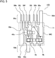
- FIG. 5 shows the internal configuration of a second semiconductor module according to embodiment 2
- FIG. 6 shows the internal configuration of a third semiconductor module according to embodiment 2.
- a first semiconductor module 102, a second semiconductor module 103, and a third semiconductor module 104 are each provided with a shared base plate 50C according to embodiment 2. It is noted that the circuit configuration of an entire system of a vehicle electric power steering device using the semiconductor module according to embodiment 2 is the same as in the above embodiment 1, and therefore FIG. 1 is applied.
- the shared base plate 50C includes a plurality of base portions 50a to which a plurality of electronic components including semiconductor switching elements are mounted, and terminal formed portions 50b extending from the base portion 50a to the outer side.
- terminals having the same functions as those on the shared base plate 50B of the first semiconductor module 100 (see FIG. 2 ) according to the above embodiment 1 are denoted by the same reference characters.
- terminals located at the same positions on the terminal formed portions 50b are denoted by the same reference characters.
- dotted-dashed lines indicate areas covered with molding resin 11.
- the first semiconductor module 102 includes one (U-phase) bridge circuit of the inverter circuit 4.
- the high-potential-side semiconductor switching element 41U is mounted to the base portion 50a that extends from the power terminal 50c.
- the source portion of the semiconductor switching element 41U is connected to the semiconductor switching element 44U via a jumper wire 45a, and is connected to the drain of the low-potential-side semiconductor switching element 42U via the jumper wire 45a and another base portion 50a.
- the semiconductor switching element 42U is connected to the shunt resistor 43U via a jumper wire and a base portion 50a, and the shunt resistor 43U is connected to the power terminal 50e which is a ground terminal.
- the power terminal 50d which is an output terminal to a motor winding extends in the upward direction in the drawing.
- the control terminals 50k, 50j, 50f, etc. are arranged alongside the power terminal 50d.
- the control terminals 50k, 50j are terminals for signals at both ends of the shunt resistor 43U, and adjacently thereto, the control terminals 50f, 50i, 50h which are gate signal terminals for the semiconductor switching elements 41U, 42U, 44U are arranged.
- a control terminal 50v branching from the power terminal 50d is used for monitoring terminal voltage of the motor 2.
- the second semiconductor module 103 shown in FIG. 5 includes the power supply relay 5 (see FIG. 1 ) as one relay function circuit.
- the semiconductor switching element 5a is mounted to the base portion 50a that leads to the power terminal 50c which is the plus power supply terminal.
- the source portion of the semiconductor switching element 5a is connected to the source portion of the semiconductor switching element 5b via a jumper wire.
- the power terminal 50d serves as an output terminal of the plus power supply.
- the source portion of the semiconductor switching element 5a is connected to another base portion 50a via a jumper wire, and in the case where voltage at the intermediate point between the semiconductor switching elements 5a, 5b needs to be monitored, the other base portion 50a is connected to the control terminal 50j via a jumper wire 45b.
- the control terminals 50f, 50h are gate signal terminals for the semiconductor switching elements 5a, 5b, respectively.
- the control terminals 50k, 50i and the power terminal 50e are not used and correspond to discrimination terminals.
- the third semiconductor module 104 shown in FIG. 6 includes the power supply relay 5 as in the second semiconductor module 103, but is different from the second semiconductor module 103 in that the power terminal 50c is used as an output terminal of the plus power supply. Therefore, the power terminal 50d is not used and corresponds to a discrimination terminal.
- the output side of the semiconductor switching element 5b, i.e., the drain thereof is connected via a long jumper wire 45c from the base portion 50a at the right end in the drawing to the base portion 50a at the left end in the drawing, and is outputted to the power terminal 50e.
- the control terminals 50i, 50v and the power terminal 50d are not used and correspond to discrimination terminals.
- the power terminal 50e which is a discrimination terminal is cut to be short, and thus the second semiconductor module 103 can be easily discriminated from the first semiconductor module 102 and the third semiconductor module 104 by outer appearances.
- the power terminal 50d which is a discrimination terminal is cut to be short, and thus the third semiconductor module 104 can be easily discriminated from the first semiconductor module 102 and the second semiconductor module 103 by outer appearances.
- one power terminal which is a discrimination terminal in each shared base plate 50C is cut.
- a control terminal which is a discrimination terminal may be cut, or a plurality of discrimination terminals may be cut.
- the same effects as in the above embodiment 1 are obtained.
Landscapes
- Engineering & Computer Science (AREA)
- Power Engineering (AREA)
- Inverter Devices (AREA)
Abstract
Description
- The present disclosure relates to a shared base plate used for a semiconductor module, and a semiconductor module provided with the shared base plate.
- A control unit of a vehicle electric power steering device includes a control circuit including a central processing unit (CPU), an inverter circuit for supplying current to three-phase windings of a motor, a power supply relay, and the like. In the case of forming such a control unit in a semiconductor module, various circuit configurations and component configurations are conceivable as follows: a configuration including one to three bridge circuits of an inverter circuit, a configuration including a power supply relay, a configuration in which some of current detection shunt resistors or switching elements are omitted, and the like.
- For example, Patent Document 1 discloses a semiconductor module including low-potential-side switching elements and high-potential-side switching elements composing an inverter circuit, power supply relays, shunt resistors as current detection means, and the like. In such a semiconductor module, the electronic components such as the semiconductor switching elements and the shunt resistors are mounted to a base plate made of copper or copper alloy, and are sealed by molding resin. In addition, a plurality of terminals such as plus and minus power supply terminals, an output (load) terminal, and a control terminal formed by the base plate are arranged outside the molding resin.
- Patent Document 1: Japanese Patent No.
5201171 - Among semiconductor modules, even if the circuit configurations thereof are different, the internal structures such as component arrangements and wiring may be considerably similar to each other. However, in conventional manufacturing of semiconductor modules, base plates corresponding to individual circuit configurations and component arrangements are designed, and therefore different base plates are used for individual products. Thus, there is a problem that the types of components are increased and the cost is increased.
- The present disclosure has been made to solve the above problem, and an object of the present disclosure is to provide a shared base plate that enables suppression of increase of the types of components of semiconductor modules, and reduce the manufacturing cost for semiconductor modules by having the shared base plates.
- A shared base plate according to the present disclosure is a shared base plate to be used for plural types of semiconductor modules different in circuit configuration or component configuration, the shared base plate including: a base portion to which a plurality of electronic components including a semiconductor switching element are to be mounted; and a terminal formed portion formed so as to extend from the base portion to an outer side, wherein the plural types of semiconductor modules include at least a first semiconductor module and a second semiconductor module, and the terminal formed portion includes a discrimination terminal which is used as a terminal in one of the first semiconductor module and the second semiconductor module and which is not used as a terminal in the other one.
- A semiconductor module according to the present disclosure is a semiconductor module including: the shared base plate according to the present disclosure; a plurality of electronic components including a semiconductor switching element and mounted to the base portion of the shared base plate; a wiring member connecting the electronic component with the base portion or another of the electronic components; and resin covering the base portion, the electronic components, and the wiring member.
- The shared base plate according to the present disclosure can be used for plural types of semiconductor modules different in circuit configuration or component configuration. Thus, components of the semiconductor modules can be standardized and increase in the types of components can be suppressed. As a result, the component cost can be reduced, so that the manufacturing cost for the semiconductor modules can be reduced.
- Objects, features, aspects, and effects of the present disclosure other than the above will become more apparent from the following detailed description with reference to the drawings.
-
- [
FIG. 1] FIG. 1 shows a circuit configuration of an entire system of a vehicle electric power steering device according to embodiment 1. - [
FIG. 2] FIG. 2 shows the internal configuration of a first semiconductor module provided with a shared base plate according to embodiment 1. - [
FIG. 3] FIG. 3 shows the internal configuration of a second semiconductor module provided with the shared base plate according to embodiment 1. - [
FIG. 4] FIG. 4 shows the internal configuration of a first semiconductor module provided with a shared base plate according toembodiment 2. - [
FIG. 5] FIG. 5 shows the internal configuration of a second semiconductor module provided with the shared base plate according toembodiment 2. - [
FIG. 6] FIG. 6 shows the internal configuration of a third semiconductor module provided with the shared base plate according toembodiment 2. - Hereinafter, a shared base plate and a semiconductor module provided with the shared base plate according to embodiment 1 will be described with reference to the drawings.
FIG. 1 shows a circuit configuration of an entire system of a vehicle electric power steering device using the semiconductor module according to embodiment 1.FIG. 2 shows the internal configuration of a first semiconductor module provided with the shared base plate according to embodiment 1, andFIG. 3 shows the internal configuration of a second semiconductor module provided with the shared base plate according to embodiment 1. In the drawings, the same or corresponding parts are denoted by the same reference characters. - As shown in
FIG. 1 , the vehicle electric power steering device includes a control unit 1, amotor 2, arotation sensor 6, asensor 8, abattery 9, anignition switch 10, and the like. Themotor 2 is a brushless motor having three-phase windings (U-phase winding 2a, V-phase winding 2b, W-phase winding 2c). Therotation sensor 6 for detecting the rotation angle of themotor 2 is provided near themotor 2. - The control unit 1 includes a
control circuit 3 having aCPU 30 as a main component, aninverter circuit 4 for supplying current to the windings of themotor 2, apower supply relay 5, and the like. Thecontrol circuit 3 includes theCPU 30, adrive circuit 31, aninput circuit 32, and apower supply circuit 33. TheCPU 30 receives an input signal from thesensor 8 such as a vehicle speed sensor or a torque sensor for detecting a steering wheel operation force, rotation angle information from therotation sensor 6, and the like, and calculates a current value for rotating themotor 2. Further, theCPU 30 outputs a control signal based on the calculation result to theinverter circuit 4 via thedrive circuit 31, to drive each switching element, and receives a current detection signal of theinverter circuit 4, to perform feedback control. - The
inverter circuit 4 has three bridge circuits corresponding to three-phase windings of themotor 2. Since the circuits for the three phases are the same, description will be given focusing on the U phase as an example. In theinverter circuit 4, asemiconductor switching element 41U as a high-potential-side switching element and asemiconductor switching element 42U as a low-potential-side switching element are connected in series to each other, and at an intermediate connection point therebetween, asemiconductor switching element 44U having a relay function capable of connection to and disconnection from a coil (load output) of themotor 2 is connected. - In addition, a
shunt resistor 43U for current detection is connected downstream of thesemiconductor switching element 42U. Theinverter circuit 4 is provided with terminals for detecting the potential difference between both ends of theshunt resistor 43U and converting the potential difference to a current value, as shown by arrows at both ends of theshunt resistor 43U inFIG. 1 . Monitor signals at various parts in theinverter circuit 4 are transmitted to theCPU 30 via theinput circuit 32 of thecontrol circuit 3. -
Smoothing capacitors power supply relay 5 is provided upstream of theinverter circuit 4, and twosemiconductor switching elements power supply relay 5 has a relay function capable of supplying power to theinverter circuit 4 and interrupting the power. - In the case of implementing the circuit configuration as shown in
FIG. 1 in a semiconductor module, various circuit configurations or component configurations are conceivable as follows: a configuration including one (or two or three) bridge circuit of theinverter circuit 4, a configuration including (or not including) thepower supply relay 5, a configuration in which some of the shunt resistors or the switching elements are omitted (or not omitted), and the like. Embodiment 1 proposes a shared base plate used for, in particular, a semiconductor module including two bridge circuits among plural types of semiconductor modules different in circuit configuration or component configuration. - The shared base plate according to embodiment 1 will be described with reference to
FIG. 2 andFIG. 3 . Aplate 50 is made of a metal material such as copper or copper alloy, and includes anouter frame 50A and a sharedbase plate 50B. InFIG. 2 andFIG. 3 , a dotted-dashed line indicates an area covered withmolding resin 11, and a broken line indicates theouter frame 50A of theplate 50. It is noted that theouter frame 50A is used for, for example, conveyance between steps in a manufacturing process for the semiconductor module, and is cut away at the time of completion. - The shared
base plate 50B can be used for plural types of semiconductor modules different in circuit configuration or component configuration, and in embodiment 1, the sharedbase plate 50B is used for afirst semiconductor module 100 shown inFIG. 2 and asecond semiconductor module 101 shown inFIG. 3 . Thefirst semiconductor module 100 has an H bridge circuit including two bridge circuits, and thesecond semiconductor module 101 has one bridge circuit and one relay function circuit (power supply relay 5 shown inFIG. 1 ) . - The shared
base plate 50B includes a plurality ofbase portions 50a to which a plurality of electronic components including thesemiconductor switching elements portions 50b formed so as to extend from thebase portions 50a to the outer side. Thebase portions 50a are also used as wiring. The terminal formedportions 50b include control terminals for input and output of control signals, and power terminals which are formed to be wider than the control terminals and through which larger currents flow than in the control terminals. - In
FIG. 2 , the upper-side terminal formedportion 50b includescontrol terminals portion 50b includespower terminals - In the
first semiconductor module 100, two bridge circuits that are the same are arranged symmetrically as shown inFIG. 2 . The U-phase bridge circuit on the left side in the drawing will be described. The high-potential-sidesemiconductor switching element 41U is mounted to thebase portion 50a that leads to thepower terminal 50c which is a plus power supply terminal. Thesemiconductor switching element 41U is connected to thesemiconductor switching element 44U via ajumper wire 45, and is further connected to the low-potential-sidesemiconductor switching element 42U. Thesemiconductor switching elements jumper wire 45 is formed from a copper plate and has a bridge shape. - The
power terminal 50d is an output terminal to the motor. Thepower terminal 50e is a ground terminal and is shared by the two bridge circuits. In light of the drive method for the three-phase winding motor, currents do not flow at the same time through ground terminals for the respective phases, and therefore thepower terminal 50e can be shared. It is noted that the ground terminal may be provided for each phase. - The
shunt resistor 43U is mounted so as to stride between thebase portions 50a.Wire bonds 46 are used for gate connection of thesemiconductor switching elements control terminals semiconductor switching elements control terminals shunt resistor 43U. Thecontrol terminal 50g is connected to the connection point among thesemiconductor switching elements - On the other hand, in the
second semiconductor module 101, a combination circuit including the power supply relay 5 (seeFIG. 1 ) and one bridge circuit is provided as shown inFIG. 3 . InFIG. 3 , the left side is the same bridge circuit as that shown inFIG. 2 , and therefore, the description thereof is omitted and the power supply relay on the right side will be described. Apower terminal 50m is a plus power supply input terminal, and thesemiconductor switching element 5a of thepower supply relay 5 is mounted to thebase portion 50a that leads to thepower terminal 50m. The source portion of thesemiconductor switching element 5a is connected to thesemiconductor switching element 5b via ajumper wire 45. Thesemiconductor switching elements - The
control terminals semiconductor switching elements semiconductor switching elements control terminal 50q leading from thebase portion 50a that is connected to thesemiconductor switching elements jumper wire 45 is used for monitoring voltage at the intermediate point between thesemiconductor switching elements control terminal 50s is at the same potential as the plus power supply of theinverter circuit 4 and is connected to apower terminal 50n. Large current flows to thepower terminal 50n, and thecontrol terminal 50s is used for monitoring. - It is noted that
control terminals second semiconductor module 101, but are used as control terminals for detecting terminal voltage at both ends of the shunt resistor in thefirst semiconductor module 100. In addition, thecontrol terminal 50q of thesecond semiconductor module 101 is used for monitoring voltage at the intermediate point between thesemiconductor switching elements first semiconductor module 100, as with thecontrol terminal 50g, thecontrol terminal 50q is connected to the connection point among the three semiconductor switching elements and is not used as a terminal. - As described above, the terminal formed
portion 50b of the sharedbase plate 50B includes discrimination terminals which are used as terminals in one of thefirst semiconductor module 100 and thesecond semiconductor module 101, and which are not used as terminals in the other one. In the examples shown inFIG. 2 andFIG. 3 , thecontrol terminals - In the case where the discrimination terminals are not used as control terminals or power terminals, the discrimination terminals may be formed to be shorter than the adjacent control terminal or power terminal. This makes it possible to easily discriminate the
first semiconductor module 100 and thesecond semiconductor module 101 by outer appearances. In embodiment 1, if thecontrol terminals second semiconductor module 101 are cut to be shorter than theadjacent control terminal 50s, thesecond semiconductor module 101 can be discriminated from thefirst semiconductor module 100. Similarly, if thecontrol terminal 50g which is not used in thefirst semiconductor module 100 is cut, thefirst semiconductor module 100 can be discriminated from thesecond semiconductor module 101. - Thus, the example in which the shared
base plate 50B is used for thefirst semiconductor module 100 and thesecond semiconductor module 101 has been described. The sharedbase plate 50B can also be used for a semiconductor module having another circuit configuration or component configuration. For example, the sharedbase plate 50B can be used for a third semiconductor module (not shown) in which a component corresponding to theshunt resistor 43U or thesemiconductor switching element 44U for U phase shown inFIG. 1 is omitted. - The third semiconductor module is the same in circuit configuration as the
first semiconductor module 100, but is different in component configuration. In the case of using the sharedbase plate 50B for the third semiconductor module, thesemiconductor switching element 44U or theshunt resistor 43U of the first semiconductor module 100 (seeFIG. 2 ) is not mounted, and the high-potential-sidesemiconductor switching element 41U is connected to the low-potential-sidesemiconductor switching element 42U via thejumper wire 45 and thebase portion 50a. In addition, the sharedbase plates 50B can also be shared by an H bridge circuit for brushless motor and an H bridge circuit for brush-equipped motor. - As described above, the shared
base plate 50B according to embodiment 1 can be used for plural types of semiconductor modules different in circuit configuration or component configuration. Thus, components can be standardized and increase in the types of components can be suppressed. As a result, the component cost can be reduced, so that the manufacturing cost for the semiconductor modules can be reduced and the number of working management processing steps can be decreased. - Further, if discrimination terminals that are not used as terminals are cut to be shorter than the adjacent other terminal, it becomes possible to easily discriminate the semiconductor module from another semiconductor module having the shared
base plate 50B by outer appearances. Thus, erroneous attachment on semiconductor modules is prevented, so that working efficiency is improved. -
FIG. 4 shows the internal configuration of a first semiconductor module according toembodiment 2,FIG. 5 shows the internal configuration of a second semiconductor module according toembodiment 2, andFIG. 6 shows the internal configuration of a third semiconductor module according toembodiment 2. Afirst semiconductor module 102, asecond semiconductor module 103, and athird semiconductor module 104 are each provided with a sharedbase plate 50C according toembodiment 2. It is noted that the circuit configuration of an entire system of a vehicle electric power steering device using the semiconductor module according toembodiment 2 is the same as in the above embodiment 1, and thereforeFIG. 1 is applied. - As shown in
FIG. 4 to FIG. 6 , the sharedbase plate 50C includes a plurality ofbase portions 50a to which a plurality of electronic components including semiconductor switching elements are mounted, and terminal formedportions 50b extending from thebase portion 50a to the outer side. In the sharedbase plate 50C of thefirst semiconductor module 102 shown inFIG. 4 , terminals having the same functions as those on the sharedbase plate 50B of the first semiconductor module 100 (seeFIG. 2 ) according to the above embodiment 1 are denoted by the same reference characters. In addition, inFIG. 4 to FIG. 6 , irrespective of the functions of terminals, terminals located at the same positions on the terminal formedportions 50b are denoted by the same reference characters. InFIG. 4 to FIG. 6 , dotted-dashed lines indicate areas covered withmolding resin 11. - As shown in
FIG. 4 , thefirst semiconductor module 102 according toembodiment 2 includes one (U-phase) bridge circuit of theinverter circuit 4. The high-potential-sidesemiconductor switching element 41U is mounted to thebase portion 50a that extends from thepower terminal 50c. The source portion of thesemiconductor switching element 41U is connected to thesemiconductor switching element 44U via ajumper wire 45a, and is connected to the drain of the low-potential-sidesemiconductor switching element 42U via thejumper wire 45a and anotherbase portion 50a. Further, thesemiconductor switching element 42U is connected to theshunt resistor 43U via a jumper wire and abase portion 50a, and theshunt resistor 43U is connected to thepower terminal 50e which is a ground terminal. - The
power terminal 50d which is an output terminal to a motor winding extends in the upward direction in the drawing. Thecontrol terminals power terminal 50d. Thecontrol terminals shunt resistor 43U, and adjacently thereto, thecontrol terminals semiconductor switching elements control terminal 50v branching from thepower terminal 50d is used for monitoring terminal voltage of themotor 2. - On the other hand, the
second semiconductor module 103 shown inFIG. 5 includes the power supply relay 5 (seeFIG. 1 ) as one relay function circuit. Thesemiconductor switching element 5a is mounted to thebase portion 50a that leads to thepower terminal 50c which is the plus power supply terminal. The source portion of thesemiconductor switching element 5a is connected to the source portion of thesemiconductor switching element 5b via a jumper wire. Thus, thepower terminal 50d serves as an output terminal of the plus power supply. - Further, the source portion of the
semiconductor switching element 5a is connected to anotherbase portion 50a via a jumper wire, and in the case where voltage at the intermediate point between thesemiconductor switching elements other base portion 50a is connected to thecontrol terminal 50j via ajumper wire 45b. Thecontrol terminals semiconductor switching elements second semiconductor module 103, thecontrol terminals power terminal 50e are not used and correspond to discrimination terminals. - The
third semiconductor module 104 shown inFIG. 6 includes thepower supply relay 5 as in thesecond semiconductor module 103, but is different from thesecond semiconductor module 103 in that thepower terminal 50c is used as an output terminal of the plus power supply. Therefore, thepower terminal 50d is not used and corresponds to a discrimination terminal. The output side of thesemiconductor switching element 5b, i.e., the drain thereof is connected via along jumper wire 45c from thebase portion 50a at the right end in the drawing to thebase portion 50a at the left end in the drawing, and is outputted to thepower terminal 50e. In thethird semiconductor module 104, thecontrol terminals power terminal 50d are not used and correspond to discrimination terminals. - As shown in
FIG. 5 , in thesecond semiconductor module 103, thepower terminal 50e which is a discrimination terminal is cut to be short, and thus thesecond semiconductor module 103 can be easily discriminated from thefirst semiconductor module 102 and thethird semiconductor module 104 by outer appearances. In addition, as shown inFIG. 6 , in thethird semiconductor module 104, thepower terminal 50d which is a discrimination terminal is cut to be short, and thus thethird semiconductor module 104 can be easily discriminated from thefirst semiconductor module 102 and thesecond semiconductor module 103 by outer appearances. - In the examples shown in
FIG. 5 andFIG. 6 , one power terminal which is a discrimination terminal in each sharedbase plate 50C is cut. However, a control terminal which is a discrimination terminal may be cut, or a plurality of discrimination terminals may be cut. Thus, also inembodiment 2, the same effects as in the above embodiment 1 are obtained. - Although the disclosure is described above in terms of various exemplary embodiments and implementations, it should be understood that the various features, aspects, and functionality described in one or more of the individual embodiments are not limited in their applicability to the particular embodiment with which they are described, but instead can be applied, alone or in various combinations to one or more of the embodiments of the disclosure. It is therefore understood that numerous modifications which have not been exemplified can be devised without departing from the scope of the present disclosure. For example, at least one of the constituent components may be modified, added, or eliminated. At least one of the constituent components mentioned in at least one of the preferred embodiments may be selected and combined with the constituent components mentioned in another preferred embodiment.
-
- 1 control unit
- 2 motor
- 2a U-phase winding
- 2b V-phase winding
- 2c W-phase winding
- 3 control circuit
- 4 inverter circuit
- 5 power supply relay
- 5a, 5b semiconductor switching element
- 6 rotation sensor
- 7U, 7V, 7W capacitor
- 8 sensor
- 9 battery
- 10 ignition switch
- 11 molding resin
- 30 CPU
- 31 drive circuit
- 32 input circuit
- 33 power supply circuit
- 41U, 42U, 44U semiconductor switching element
- 43U shunt resistor
- 45, 45a, 45b, 45c jumper wire
- 46 wire bond
- 50 plate
- 50A outer frame
- 50B, 50C shared base plate
- 50a base portion
- 50b terminal formed portion
- 50c, 50d, 50e, 50m, 50n power terminal
- 50f, 50g, 50h, 50i, 50j, 50k, 50p, 50q, 50r, 50s, 50t, 50u, 50v control terminal
- 100 first semiconductor module
- 101 second semiconductor module
- 102 first semiconductor module
- 103 second semiconductor module
- 104 third semiconductor module
Claims (8)
- A shared base plate to be used for plural types of semiconductor modules different in circuit configuration or component configuration, the shared base plate comprising:a base portion to which a plurality of electronic components including a semiconductor switching element are to be mounted; anda terminal formed portion formed so as to extend from the base portion to an outer side, whereinthe plural types of semiconductor modules include at least a first semiconductor module and a second semiconductor module, andthe terminal formed portion includes a discrimination terminal which is used as a terminal in one of the first semiconductor module and the second semiconductor module and which is not used as a terminal in the other one.
- The shared base plate according to claim 1, wherein
the terminal formed portion includes a control terminal for input and output of a control signal, and a power terminal which is formed to be wider than the control terminal and through which larger current flows than in the control terminal. - The shared base plate according to claim 2, wherein
the discrimination terminal is used as the control terminal in the first semiconductor module or the second semiconductor module. - The shared base plate according to claim 2, wherein
the discrimination terminal is used as the power terminal in the first semiconductor module or the second semiconductor module. - The shared base plate according to claim 2, wherein
when the discrimination terminal is not used as the control terminal or the power terminal, the discrimination terminal is formed to be shorter than the adjacent control terminal or the adjacent power terminal. - The shared base plate according to any one of claims 1 to 5, wherein
the first semiconductor module has at least one bridge circuit, and the second semiconductor module has one relay function circuit. - The shared base plate according to any one of claims 1 to 5, wherein
the first semiconductor module has two bridge circuits, and the second semiconductor module has one bridge circuit and one relay function circuit. - A semiconductor module comprising:the shared base plate according to any one of claims 1 to 7;a plurality of electronic components including a semiconductor switching element and mounted to the base portion of the shared base plate;a wiring member connecting the electronic component with the base portion or another of the electronic components; andresin covering the base portion, the electronic components, and the wiring member.
Applications Claiming Priority (1)
| Application Number | Priority Date | Filing Date | Title |
|---|---|---|---|
| PCT/JP2018/016734 WO2019207664A1 (en) | 2018-04-25 | 2018-04-25 | Shared base plate and semiconductor module provided with same |
Publications (2)
| Publication Number | Publication Date |
|---|---|
| EP3787019A1 true EP3787019A1 (en) | 2021-03-03 |
| EP3787019A4 EP3787019A4 (en) | 2021-05-05 |
Family
ID=68294804
Family Applications (1)
| Application Number | Title | Priority Date | Filing Date |
|---|---|---|---|
| EP18915898.3A Withdrawn EP3787019A4 (en) | 2018-04-25 | 2018-04-25 | SHARED BASE PLATE AND SEMICONDUCTOR MODULE INCLUDING IT |
Country Status (5)
| Country | Link |
|---|---|
| US (1) | US11626347B2 (en) |
| EP (1) | EP3787019A4 (en) |
| JP (1) | JP6991316B2 (en) |
| CN (1) | CN111989774B (en) |
| WO (1) | WO2019207664A1 (en) |
Families Citing this family (2)
| Publication number | Priority date | Publication date | Assignee | Title |
|---|---|---|---|---|
| US20240387442A1 (en) * | 2021-10-08 | 2024-11-21 | Mitsubishi Electric Corporation | Semiconductor module and method for manufacturing same |
| WO2023170897A1 (en) * | 2022-03-11 | 2023-09-14 | 三菱電機株式会社 | Semiconductor module |
Family Cites Families (13)
| Publication number | Priority date | Publication date | Assignee | Title |
|---|---|---|---|---|
| JPS521171B2 (en) | 1972-10-11 | 1977-01-12 | ||
| JPS62274645A (en) * | 1986-05-23 | 1987-11-28 | Hitachi Ltd | Lead frame and electronic device using the same |
| US5084753A (en) * | 1989-01-23 | 1992-01-28 | Analog Devices, Inc. | Packaging for multiple chips on a single leadframe |
| US5049973A (en) * | 1990-06-26 | 1991-09-17 | Harris Semiconductor Patents, Inc. | Heat sink and multi mount pad lead frame package and method for electrically isolating semiconductor die(s) |
| KR100306988B1 (en) * | 1992-10-26 | 2001-12-15 | 윌리엄 비. 켐플러 | Device Package |
| JP3420153B2 (en) * | 2000-01-24 | 2003-06-23 | Necエレクトロニクス株式会社 | Semiconductor device and manufacturing method thereof |
| JP5201171B2 (en) | 2010-05-21 | 2013-06-05 | 株式会社デンソー | Semiconductor module and driving device using the same |
| JP5397417B2 (en) * | 2011-05-30 | 2014-01-22 | 株式会社デンソー | Semiconductor device and driving device using the same |
| US9087829B2 (en) | 2011-08-05 | 2015-07-21 | Infineon Technologies Ag | Semiconductor arrangement |
| JP5477669B2 (en) | 2012-02-28 | 2014-04-23 | 株式会社デンソー | Semiconductor module |
| JP5569555B2 (en) * | 2012-05-17 | 2014-08-13 | 株式会社デンソー | Wiring member and semiconductor module using the same |
| JP5586671B2 (en) * | 2012-09-28 | 2014-09-10 | 三菱電機株式会社 | Power module and driving device using the same |
| WO2017154189A1 (en) * | 2016-03-11 | 2017-09-14 | 新電元工業株式会社 | Semiconductor device |
-
2018
- 2018-04-25 JP JP2020515356A patent/JP6991316B2/en active Active
- 2018-04-25 US US16/975,195 patent/US11626347B2/en active Active
- 2018-04-25 EP EP18915898.3A patent/EP3787019A4/en not_active Withdrawn
- 2018-04-25 CN CN201880092539.0A patent/CN111989774B/en active Active
- 2018-04-25 WO PCT/JP2018/016734 patent/WO2019207664A1/en not_active Ceased
Also Published As
| Publication number | Publication date |
|---|---|
| JP6991316B2 (en) | 2022-01-12 |
| CN111989774A (en) | 2020-11-24 |
| US20200395271A1 (en) | 2020-12-17 |
| JPWO2019207664A1 (en) | 2021-01-14 |
| CN111989774B (en) | 2024-07-02 |
| EP3787019A4 (en) | 2021-05-05 |
| US11626347B2 (en) | 2023-04-11 |
| WO2019207664A1 (en) | 2019-10-31 |
Similar Documents
| Publication | Publication Date | Title |
|---|---|---|
| US9647599B2 (en) | Electronic apparatus | |
| CN109586517B (en) | Circuit board, motor drive device, and electric power steering device | |
| US10998842B2 (en) | Power conversion device, motor drive unit, and electric power steering device | |
| US12155276B2 (en) | Electric power steering apparatus | |
| CN106716822B (en) | Inverter device for multi-phase AC motor drive | |
| US20200321902A1 (en) | Abnormality detection device | |
| EP2299587A2 (en) | Motor drive device capable of detecting a fault condition | |
| US9312683B2 (en) | Vehicle-mounted electric rotating machine | |
| JP7124716B2 (en) | Motor drive device and electric power steering device | |
| CN114189194A (en) | Motor control device, motor unit, and vehicle | |
| EP3787019A1 (en) | Shared base plate and semiconductor module provided with same | |
| US10056752B2 (en) | Rotary electric machine for a vehicle | |
| EP3010137B1 (en) | Multilevel inverter | |
| JP2020010509A (en) | Power converter | |
| CN110392977A (en) | Power inverter, motor drive unit and electric power steering apparatus | |
| EP2073370B1 (en) | Motor control device | |
| EP4325711A1 (en) | Power conversion device | |
| EP4156252B1 (en) | Semiconductor module and method of manufacturing semiconductor module | |
| EP4415040A1 (en) | Semiconductor module and method for manufacturing same | |
| JP2013021748A (en) | Intelligent module | |
| EP4227987A1 (en) | Semiconductor module | |
| EP2894775A1 (en) | Intelligent module | |
| CN118202570A (en) | Motor driving device | |
| WO2020110875A1 (en) | Motor control device | |
| KR20170027186A (en) | Control apparatus of electronic active rolling stabilizer system and method thereof |
Legal Events
| Date | Code | Title | Description |
|---|---|---|---|
| STAA | Information on the status of an ep patent application or granted ep patent |
Free format text: STATUS: THE INTERNATIONAL PUBLICATION HAS BEEN MADE |
|
| PUAI | Public reference made under article 153(3) epc to a published international application that has entered the european phase |
Free format text: ORIGINAL CODE: 0009012 |
|
| STAA | Information on the status of an ep patent application or granted ep patent |
Free format text: STATUS: REQUEST FOR EXAMINATION WAS MADE |
|
| 17P | Request for examination filed |
Effective date: 20200907 |
|
| AK | Designated contracting states |
Kind code of ref document: A1 Designated state(s): AL AT BE BG CH CY CZ DE DK EE ES FI FR GB GR HR HU IE IS IT LI LT LU LV MC MK MT NL NO PL PT RO RS SE SI SK SM TR |
|
| AX | Request for extension of the european patent |
Extension state: BA ME |
|
| REG | Reference to a national code |
Ref country code: DE Ref legal event code: R079 Free format text: PREVIOUS MAIN CLASS: H01L0023480000 Ipc: H01L0023495000 |
|
| A4 | Supplementary search report drawn up and despatched |
Effective date: 20210406 |
|
| RIC1 | Information provided on ipc code assigned before grant |
Ipc: H01L 23/495 20060101AFI20210329BHEP Ipc: H02M 7/48 20070101ALI20210329BHEP Ipc: H02M 7/00 20060101ALI20210329BHEP Ipc: H01L 23/48 20060101ALI20210329BHEP Ipc: H02M 7/5387 20070101ALI20210329BHEP |
|
| DAV | Request for validation of the european patent (deleted) | ||
| DAX | Request for extension of the european patent (deleted) | ||
| STAA | Information on the status of an ep patent application or granted ep patent |
Free format text: STATUS: THE APPLICATION HAS BEEN WITHDRAWN |
|
| 18W | Application withdrawn |
Effective date: 20251112 |