EP3786518A1 - Illumination device - Google Patents
Illumination device Download PDFInfo
- Publication number
- EP3786518A1 EP3786518A1 EP19193848.9A EP19193848A EP3786518A1 EP 3786518 A1 EP3786518 A1 EP 3786518A1 EP 19193848 A EP19193848 A EP 19193848A EP 3786518 A1 EP3786518 A1 EP 3786518A1
- Authority
- EP
- European Patent Office
- Prior art keywords
- illumination device
- light emitting
- light
- light source
- emitting devices
- Prior art date
- Legal status (The legal status is an assumption and is not a legal conclusion. Google has not performed a legal analysis and makes no representation as to the accuracy of the status listed.)
- Pending
Links
Images


Classifications
-
- F—MECHANICAL ENGINEERING; LIGHTING; HEATING; WEAPONS; BLASTING
- F21—LIGHTING
- F21K—NON-ELECTRIC LIGHT SOURCES USING LUMINESCENCE; LIGHT SOURCES USING ELECTROCHEMILUMINESCENCE; LIGHT SOURCES USING CHARGES OF COMBUSTIBLE MATERIAL; LIGHT SOURCES USING SEMICONDUCTOR DEVICES AS LIGHT-GENERATING ELEMENTS; LIGHT SOURCES NOT OTHERWISE PROVIDED FOR
- F21K9/00—Light sources using semiconductor devices as light-generating elements, e.g. using light-emitting diodes [LED] or lasers
- F21K9/60—Optical arrangements integrated in the light source, e.g. for improving the colour rendering index or the light extraction
- F21K9/69—Details of refractors forming part of the light source
-
- F—MECHANICAL ENGINEERING; LIGHTING; HEATING; WEAPONS; BLASTING
- F21—LIGHTING
- F21S—NON-PORTABLE LIGHTING DEVICES; SYSTEMS THEREOF; VEHICLE LIGHTING DEVICES SPECIALLY ADAPTED FOR VEHICLE EXTERIORS
- F21S41/00—Illuminating devices specially adapted for vehicle exteriors, e.g. headlamps
- F21S41/10—Illuminating devices specially adapted for vehicle exteriors, e.g. headlamps characterised by the light source
- F21S41/14—Illuminating devices specially adapted for vehicle exteriors, e.g. headlamps characterised by the light source characterised by the type of light source
- F21S41/141—Light emitting diodes [LED]
- F21S41/151—Light emitting diodes [LED] arranged in one or more lines
- F21S41/153—Light emitting diodes [LED] arranged in one or more lines arranged in a matrix
-
- F—MECHANICAL ENGINEERING; LIGHTING; HEATING; WEAPONS; BLASTING
- F21—LIGHTING
- F21S—NON-PORTABLE LIGHTING DEVICES; SYSTEMS THEREOF; VEHICLE LIGHTING DEVICES SPECIALLY ADAPTED FOR VEHICLE EXTERIORS
- F21S2/00—Systems of lighting devices, not provided for in main groups F21S4/00 - F21S10/00 or F21S19/00, e.g. of modular construction
- F21S2/005—Systems of lighting devices, not provided for in main groups F21S4/00 - F21S10/00 or F21S19/00, e.g. of modular construction of modular construction
-
- F—MECHANICAL ENGINEERING; LIGHTING; HEATING; WEAPONS; BLASTING
- F21—LIGHTING
- F21S—NON-PORTABLE LIGHTING DEVICES; SYSTEMS THEREOF; VEHICLE LIGHTING DEVICES SPECIALLY ADAPTED FOR VEHICLE EXTERIORS
- F21S41/00—Illuminating devices specially adapted for vehicle exteriors, e.g. headlamps
- F21S41/10—Illuminating devices specially adapted for vehicle exteriors, e.g. headlamps characterised by the light source
- F21S41/14—Illuminating devices specially adapted for vehicle exteriors, e.g. headlamps characterised by the light source characterised by the type of light source
- F21S41/141—Light emitting diodes [LED]
- F21S41/143—Light emitting diodes [LED] the main emission direction of the LED being parallel to the optical axis of the illuminating device
-
- F—MECHANICAL ENGINEERING; LIGHTING; HEATING; WEAPONS; BLASTING
- F21—LIGHTING
- F21S—NON-PORTABLE LIGHTING DEVICES; SYSTEMS THEREOF; VEHICLE LIGHTING DEVICES SPECIALLY ADAPTED FOR VEHICLE EXTERIORS
- F21S41/00—Illuminating devices specially adapted for vehicle exteriors, e.g. headlamps
- F21S41/20—Illuminating devices specially adapted for vehicle exteriors, e.g. headlamps characterised by refractors, transparent cover plates, light guides or filters
- F21S41/25—Projection lenses
-
- F—MECHANICAL ENGINEERING; LIGHTING; HEATING; WEAPONS; BLASTING
- F21—LIGHTING
- F21S—NON-PORTABLE LIGHTING DEVICES; SYSTEMS THEREOF; VEHICLE LIGHTING DEVICES SPECIALLY ADAPTED FOR VEHICLE EXTERIORS
- F21S41/00—Illuminating devices specially adapted for vehicle exteriors, e.g. headlamps
- F21S41/60—Illuminating devices specially adapted for vehicle exteriors, e.g. headlamps characterised by a variable light distribution
- F21S41/65—Illuminating devices specially adapted for vehicle exteriors, e.g. headlamps characterised by a variable light distribution by acting on light sources
- F21S41/663—Illuminating devices specially adapted for vehicle exteriors, e.g. headlamps characterised by a variable light distribution by acting on light sources by switching light sources
-
- F—MECHANICAL ENGINEERING; LIGHTING; HEATING; WEAPONS; BLASTING
- F21—LIGHTING
- F21V—FUNCTIONAL FEATURES OR DETAILS OF LIGHTING DEVICES OR SYSTEMS THEREOF; STRUCTURAL COMBINATIONS OF LIGHTING DEVICES WITH OTHER ARTICLES, NOT OTHERWISE PROVIDED FOR
- F21V11/00—Screens not covered by groups F21V1/00, F21V3/00, F21V7/00 or F21V9/00
-
- F—MECHANICAL ENGINEERING; LIGHTING; HEATING; WEAPONS; BLASTING
- F21—LIGHTING
- F21V—FUNCTIONAL FEATURES OR DETAILS OF LIGHTING DEVICES OR SYSTEMS THEREOF; STRUCTURAL COMBINATIONS OF LIGHTING DEVICES WITH OTHER ARTICLES, NOT OTHERWISE PROVIDED FOR
- F21V19/00—Fastening of light sources or lamp holders
- F21V19/001—Fastening of light sources or lamp holders the light sources being semiconductors devices, e.g. LEDs
-
- F—MECHANICAL ENGINEERING; LIGHTING; HEATING; WEAPONS; BLASTING
- F21—LIGHTING
- F21V—FUNCTIONAL FEATURES OR DETAILS OF LIGHTING DEVICES OR SYSTEMS THEREOF; STRUCTURAL COMBINATIONS OF LIGHTING DEVICES WITH OTHER ARTICLES, NOT OTHERWISE PROVIDED FOR
- F21V23/00—Arrangement of electric circuit elements in or on lighting devices
- F21V23/003—Arrangement of electric circuit elements in or on lighting devices the elements being electronics drivers or controllers for operating the light source, e.g. for a LED array
-
- F—MECHANICAL ENGINEERING; LIGHTING; HEATING; WEAPONS; BLASTING
- F21—LIGHTING
- F21V—FUNCTIONAL FEATURES OR DETAILS OF LIGHTING DEVICES OR SYSTEMS THEREOF; STRUCTURAL COMBINATIONS OF LIGHTING DEVICES WITH OTHER ARTICLES, NOT OTHERWISE PROVIDED FOR
- F21V9/00—Elements for modifying spectral properties, polarisation or intensity of the light emitted, e.g. filters
- F21V9/30—Elements containing photoluminescent material distinct from or spaced from the light source
- F21V9/32—Elements containing photoluminescent material distinct from or spaced from the light source characterised by the arrangement of the photoluminescent material
-
- G—PHYSICS
- G02—OPTICS
- G02B—OPTICAL ELEMENTS, SYSTEMS OR APPARATUS
- G02B27/00—Optical systems or apparatus not provided for by any of the groups G02B1/00 - G02B26/00, G02B30/00
- G02B27/30—Collimators
-
- H—ELECTRICITY
- H01—ELECTRIC ELEMENTS
- H01L—SEMICONDUCTOR DEVICES NOT COVERED BY CLASS H10
- H01L25/00—Assemblies consisting of a plurality of individual semiconductor or other solid state devices ; Multistep manufacturing processes thereof
- H01L25/03—Assemblies consisting of a plurality of individual semiconductor or other solid state devices ; Multistep manufacturing processes thereof all the devices being of a type provided for in the same subgroup of groups H01L27/00 - H01L33/00, or in a single subclass of H10K, H10N, e.g. assemblies of rectifier diodes
- H01L25/04—Assemblies consisting of a plurality of individual semiconductor or other solid state devices ; Multistep manufacturing processes thereof all the devices being of a type provided for in the same subgroup of groups H01L27/00 - H01L33/00, or in a single subclass of H10K, H10N, e.g. assemblies of rectifier diodes the devices not having separate containers
- H01L25/075—Assemblies consisting of a plurality of individual semiconductor or other solid state devices ; Multistep manufacturing processes thereof all the devices being of a type provided for in the same subgroup of groups H01L27/00 - H01L33/00, or in a single subclass of H10K, H10N, e.g. assemblies of rectifier diodes the devices not having separate containers the devices being of a type provided for in group H01L33/00
- H01L25/0753—Assemblies consisting of a plurality of individual semiconductor or other solid state devices ; Multistep manufacturing processes thereof all the devices being of a type provided for in the same subgroup of groups H01L27/00 - H01L33/00, or in a single subclass of H10K, H10N, e.g. assemblies of rectifier diodes the devices not having separate containers the devices being of a type provided for in group H01L33/00 the devices being arranged next to each other
-
- F—MECHANICAL ENGINEERING; LIGHTING; HEATING; WEAPONS; BLASTING
- F21—LIGHTING
- F21S—NON-PORTABLE LIGHTING DEVICES; SYSTEMS THEREOF; VEHICLE LIGHTING DEVICES SPECIALLY ADAPTED FOR VEHICLE EXTERIORS
- F21S41/00—Illuminating devices specially adapted for vehicle exteriors, e.g. headlamps
- F21S41/10—Illuminating devices specially adapted for vehicle exteriors, e.g. headlamps characterised by the light source
- F21S41/14—Illuminating devices specially adapted for vehicle exteriors, e.g. headlamps characterised by the light source characterised by the type of light source
- F21S41/141—Light emitting diodes [LED]
- F21S41/151—Light emitting diodes [LED] arranged in one or more lines
-
- F—MECHANICAL ENGINEERING; LIGHTING; HEATING; WEAPONS; BLASTING
- F21—LIGHTING
- F21S—NON-PORTABLE LIGHTING DEVICES; SYSTEMS THEREOF; VEHICLE LIGHTING DEVICES SPECIALLY ADAPTED FOR VEHICLE EXTERIORS
- F21S8/00—Lighting devices intended for fixed installation
- F21S8/08—Lighting devices intended for fixed installation with a standard
- F21S8/085—Lighting devices intended for fixed installation with a standard of high-built type, e.g. street light
-
- F—MECHANICAL ENGINEERING; LIGHTING; HEATING; WEAPONS; BLASTING
- F21—LIGHTING
- F21Y—INDEXING SCHEME ASSOCIATED WITH SUBCLASSES F21K, F21L, F21S and F21V, RELATING TO THE FORM OR THE KIND OF THE LIGHT SOURCES OR OF THE COLOUR OF THE LIGHT EMITTED
- F21Y2103/00—Elongate light sources, e.g. fluorescent tubes
- F21Y2103/10—Elongate light sources, e.g. fluorescent tubes comprising a linear array of point-like light-generating elements
-
- F—MECHANICAL ENGINEERING; LIGHTING; HEATING; WEAPONS; BLASTING
- F21—LIGHTING
- F21Y—INDEXING SCHEME ASSOCIATED WITH SUBCLASSES F21K, F21L, F21S and F21V, RELATING TO THE FORM OR THE KIND OF THE LIGHT SOURCES OR OF THE COLOUR OF THE LIGHT EMITTED
- F21Y2105/00—Planar light sources
- F21Y2105/10—Planar light sources comprising a two-dimensional array of point-like light-generating elements
- F21Y2105/12—Planar light sources comprising a two-dimensional array of point-like light-generating elements characterised by the geometrical disposition of the light-generating elements, e.g. arranging light-generating elements in differing patterns or densities
-
- F—MECHANICAL ENGINEERING; LIGHTING; HEATING; WEAPONS; BLASTING
- F21—LIGHTING
- F21Y—INDEXING SCHEME ASSOCIATED WITH SUBCLASSES F21K, F21L, F21S and F21V, RELATING TO THE FORM OR THE KIND OF THE LIGHT SOURCES OR OF THE COLOUR OF THE LIGHT EMITTED
- F21Y2115/00—Light-generating elements of semiconductor light sources
- F21Y2115/10—Light-emitting diodes [LED]
-
- H—ELECTRICITY
- H01—ELECTRIC ELEMENTS
- H01L—SEMICONDUCTOR DEVICES NOT COVERED BY CLASS H10
- H01L33/00—Semiconductor devices with at least one potential-jump barrier or surface barrier specially adapted for light emission; Processes or apparatus specially adapted for the manufacture or treatment thereof or of parts thereof; Details thereof
- H01L33/44—Semiconductor devices with at least one potential-jump barrier or surface barrier specially adapted for light emission; Processes or apparatus specially adapted for the manufacture or treatment thereof or of parts thereof; Details thereof characterised by the coatings, e.g. passivation layer or anti-reflective coating
- H01L33/46—Reflective coating, e.g. dielectric Bragg reflector
-
- H—ELECTRICITY
- H01—ELECTRIC ELEMENTS
- H01L—SEMICONDUCTOR DEVICES NOT COVERED BY CLASS H10
- H01L33/00—Semiconductor devices with at least one potential-jump barrier or surface barrier specially adapted for light emission; Processes or apparatus specially adapted for the manufacture or treatment thereof or of parts thereof; Details thereof
- H01L33/48—Semiconductor devices with at least one potential-jump barrier or surface barrier specially adapted for light emission; Processes or apparatus specially adapted for the manufacture or treatment thereof or of parts thereof; Details thereof characterised by the semiconductor body packages
- H01L33/50—Wavelength conversion elements
-
- H—ELECTRICITY
- H01—ELECTRIC ELEMENTS
- H01L—SEMICONDUCTOR DEVICES NOT COVERED BY CLASS H10
- H01L33/00—Semiconductor devices with at least one potential-jump barrier or surface barrier specially adapted for light emission; Processes or apparatus specially adapted for the manufacture or treatment thereof or of parts thereof; Details thereof
- H01L33/48—Semiconductor devices with at least one potential-jump barrier or surface barrier specially adapted for light emission; Processes or apparatus specially adapted for the manufacture or treatment thereof or of parts thereof; Details thereof characterised by the semiconductor body packages
- H01L33/58—Optical field-shaping elements
-
- H—ELECTRICITY
- H01—ELECTRIC ELEMENTS
- H01L—SEMICONDUCTOR DEVICES NOT COVERED BY CLASS H10
- H01L33/00—Semiconductor devices with at least one potential-jump barrier or surface barrier specially adapted for light emission; Processes or apparatus specially adapted for the manufacture or treatment thereof or of parts thereof; Details thereof
- H01L33/48—Semiconductor devices with at least one potential-jump barrier or surface barrier specially adapted for light emission; Processes or apparatus specially adapted for the manufacture or treatment thereof or of parts thereof; Details thereof characterised by the semiconductor body packages
- H01L33/62—Arrangements for conducting electric current to or from the semiconductor body, e.g. lead-frames, wire-bonds or solder balls
Definitions
- the invention relates to illumination devices. More specifically, the invention relates to illumination devices comprising a plurality of LED light source devices.
- LED based illumination devices have replaced conventional light source devices, e.g. incandescent light source devices, in many applications. Especially the low energy consumption, long lifetime, and high variability in colour and colour temperature make LED based illumination devices a preferred choice for most applications.
- LED based illumination devices usually comprise a plurality of individual light emitting devices, each comprising an LED light source device.
- the plurality of individual light emitting devices are commonly arranged in arrays, e.g. linear arrays.
- directional illumination is required.
- the light emitted by the plurality of light emitting devices is collimated by optical systems, such that the light of each of the light emitting devices is shaped into a light beam with a narrow cone angle.
- a possible cone angle of a light beam can be 2°.
- LED light source devices used in illumination devices usually comprise an LED chip for emitting excitation light, and a phosphor body covering the LED chip for converting excitation light into illumination light of a predetermined colour temperature. Because LED chips always emit light within a narrow wavelength bandwidth, such light is usually not well suited for illumination purposes. Therefore, phosphors are used to convert some or all of the light emitted by the LED chip into illumination light of a predetermined colour temperature. The colour temperature can be determined based on the specific application of the illumination device.
- LED light sources When a plurality of LED light source devices are placed in close proximity to each other, excitation light of one LED chip can travel into the phosphor body of a neighbouring LED light source device. This effect reduces the contrast available by selectively activating or deactivating individual LED light sources.
- known LED light sources therefore further comprise a light blocking layer on the lateral surfaces of the LED chip and/or the phosphor body.
- the light blocking layer may comprise silicon mixed with titanium dioxide particles.
- the light blocking layer is sometimes also referred to as side coating.
- arrays of LED light sources always comprise dark surface portions interposed between light emitting surface portions, irrespective of how tight the individual LED light sources are packed in the array. Due to further technical constraints, e.g. handling of individual LED light sources during manufacturing, LED light sources cannot be packed in an array without gaps. Even if such technical constraints can be overcome, packing LED light sources in an array creates problems with heat management.
- the resulting illumination field When light emitted by an array of LED light sources, which comprises dark surface portions interposed between light emitting surface portions, is collimated by an optical system, the resulting illumination field has a comb-like structure with individual beams, emanating from the individual LED light sources, separated by gaps.
- Such illumination fields can be disadvantageous, e.g. when used for illumination of a road by vehicle headlights or street lights, or for illumination of a workspace by a room light.
- the gaps in the illumination field can be reduced or even completely removed by modification of the optical system for collimation of the light.
- modifications increase the complexity of the optical system, and therefore make the illumination device more expensive.
- an illumination device comprising a plurality of LED light source devices arranged in an array, which provides for a light field with improved homogeneity.
- an illumination device comprising a plurality of LED light source devices arranged in an array, and with an optical system of reduced complexity.
- an illumination device comprising a plurality of LED light source devices arranged in an array, which provides for improved heat management.
- an illumination device is provided with a plurality of light emitting devices and an optical system for collimating light emitted by the plurality of light emitting devices, wherein each of the light emitting devices comprises an LED light source device having an LED chip for emitting excitation light, a phosphor body covering the LED chip for converting excitation light into illumination light of a predetermined colour temperature, and a light blocking layer arranged on the lateral surfaces of the LED chip and/or the phosphor body, wherein a first group of the light emitting devices are arranged in a first linear array having first gaps, and a first optical system is arranged near the first group of light emitting devices, an optical axis of the first optical system being substantially orthogonal to the first linear array, wherein at least one second group of the light emitting devices are arranged in at least one second linear array parallel to the first linear array, having second gaps, at least one second optical system is arranged near the at least one second group of light emitting devices, an optical axis of the second optical system being substantially orthogon
- the inventive illumination device uses two optical systems, each providing an partial illumination field with gaps due to the gaps between LED light source devices in the respective arrays, wherein the partial illumination fields superimpose so that the light beams of one partial illumination field meet the gaps of the other partial illumination field, and vice versa.
- the resulting illumination field can be substantially gap-free.
- the resulting illumination field is substantially gap-free at the predetermined distance, it is understood that the resulting illumination field preferably remains substantially gap-free at distances greater than the predetermined distance.
- Each of the LED light source devices may have a light emitting surface with a predetermined first width in the direction of the first or second array.
- Each of the gaps between neighbouring LED light source devices may have a predetermined second width in the direction of the first or second array.
- the first and second width may be selected so that the distance between the light emitting surfaces of neighbouring LED light source devices substantially equal an integer multiple of the first width.
- the distance between the light emitting surfaces of neighbouring LED light source devices may substantially equal the first width.
- the optical axes of the first and second optical system may be substantially parallel to each other.
- the position of the light source devices of the second group of light source devices relative to the optical axis of the second optical system may be offset with respect to the position of the light source devices of the first group of light source devices relative to the optical axis of the first optical system.
- the first and second arrays may be arranged along a base line parallel to the first and second arrays.
- the first and second arrays may arranged along a base line orthogonal to the first and second arrays.
- the first width may between 0,5mm and 1mm.
- the first and second optical systems may comprise positive lenses.
- the first and second arrays may be substantially arranged in the focus planes of respective positive lenses.
- the first and second groups of light emitting devices may be placed on first and second printed circuit boards.
- the first and second groups of light emitting devices may be placed on a common printed circuit board.
- the illumination device may further comprise a control unit capable of selectively activating / deactivating individual light emitting devices of the plurality of light emitting devices.
- the illumination device may be a vehicle headlight, and the predetermined distance from the illumination device may be between 20m and 30m, preferably 25m.
- the illumination device may be a street light, and the predetermined distance from the illumination device may be between 3m and 6m.
- the illumination device may be a room light, and the predetermined distance from the illumination device may be between 2m and 4m.
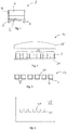
- Fig. 1 shows an LED light source device 1 in a sectional view.
- the LED light source device 1 comprises an LED chip 2 connected to a first lead frame 3 with an anode side of the LED chip 2.
- a cathode side of the LED chip 2 is connected to a second lead frame 4.
- the lead frames 3, 4 may be omitted, and solder contacts may be directly provided on a surface of the LED chip.
- the LED chip 2 is embedded in a phosphor body 6.
- the phosphor body 6 serves to convert narrow-bandwidth light emitted by the LED chip 2 into illumination light of a desired colour temperature.
- the phosphor body 6 can also serve to mechanically connect first and second lead frames 3, 4.
- Phosphor body 6 can comprise a transparent resin with immersed phosphor particles (not shown).
- the phosphor particles can comprise one or more different types of phosphor, selected to provide a desired colour temperature of the illumination light.
- the lateral sides of the phosphor body 6 are surrounded by a light blocking layer, also referred to as reflector layer 7.
- the reflector layer 7 is provided so that excitation light and/or illumination light cannot exit the LED light source device 1 at the lateral sides thereof and enter into neighbouring LED light source devices. Such cross-illumination would reduce the available contrast of an illumination device using the LED light source devices, which is undesirable.
- the reflector layer 7 may consist of silicon with embedded TiO2 particles. It is sometimes also referred to as side coating.
- LED light source devices Due to the described design of LED light source devices, such devices always comprise a light emitting surface portion surrounded by a surface which does not emit light.
- the light emitting surface portion can have a size of about 1mm 2 or less, for example between 0,5mm 2 and 1mm 2 .
- the reflector layer 7 may have a thickness of about 0,01 mm or less.
- Fig. 2 depicts an illumination device 10 comprising a plurality of LED light source devices 1 arranged on a circuit board 11 in a linear array 12.
- a lens 15 is provided for collimating the light emitted by the individual LED light source devices 1. Therefore, the light emitting surface portions of the LED light source devices 1 are approximately placed in focal plane of the lens 15. While the lens 15 is depicted as a single lens, it may equally comprise a plurality of lenses forming an optical system. Such an optical system may e.g. provide for colour correction of the illumination light, length and/or weight reduction of the optical system, or both.
- the optical system may comprise reflective elements instead of or in addition to lenses.
- Fig. 3 depicts the array 12 of LED light source devices 1 in a plan view.
- the individual LED light source devices 1 are positioned to leave gaps 20 between neighbouring LED light source devices 1.
- the gaps 20 are necessary for several reasons. One reason is that it is difficult to place the LED light sources 1 without gaps 20 in an automated process, as each automated process has to provide for positional tolerances. Another reason is that the gaps 20 provide for dissipation of heat created in the individual LED light source devices 1. A further reason may be that lead frames of neighbouring LED light source devices need to have a minimum distance to avoid short-circuits.
- the light emitting surface portions of neighbouring LED light source devices 1 in the array 12 are separated by a distance d equalling the width of a gap 20 plus the double width of a reflector layer 7.
- FIG. 4 A possible light field emitted by the illumination device of Fig. 2 is depicted in Fig. 4 .
- the light field is defined by the projection of the light emitted by individual LED light source devices 1 through the lens 15 onto a reference plane 35.
- the reference plane may be 25 meters away from the illumination device.
- the light field consist of several light beams 30 separated by dark spaces 31.
- the dark spaces 31 can be seen as projections of the gaps 20 and the reflector layers 7, which separate the light emitting surface portions of the LED light source devices 1.
- An improved illumination device 100 is depicted in Fig. 5 .
- the illumination device 100 comprises a first group of LED light source devices 101 arranged in a first array 102. Individual LED light source devices 101 are separated from neighbouring LED light source devices 101 by gaps 103.
- a first lens 105 is positioned near the first array 102 of LED light source devices, so that an optical axis 106 of the first lens 105 is approximately orthogonal to the first array 102, and the light emitting surfaces of the first group of LED light source devices 101 are positioned in approximately in a focal plane of the first lens 105.
- the first lens 105 can be a single lens or an optical system comprising more than one optical elements, as described above with reference to Fig. 2 .
- a second group of LED light source devices 111 is arranged in a second array 112 located next to the first array 102. Again, individual LED light source devices 111 are separated by gaps 113.
- a second lens 115 is positioned so that an optical axis 116 of the second lens 115 is approximately orthogonal to the second array 112, and the light emitting surfaces of the LED light source devices 111 are positioned approximately in a focal plane of the second lens 115.
- the light field emitted by the first array 101 of LED light source devices 101 is depicted in Fig, 6a .
- the light field emitted by the second array of LED light source devices 111 is depicted in Fig. 6b .
- the light fields depicted in Figs. 6a, 6b comprise light beams 120, 121, corresponding to the light emitting surface portions of LED light source devices 101, 111, separated by dark spaces 122, 123, corresponding to the gaps 103, 113 of the first and second arrays 102, 112 and the non-light-emitting surface portions the LED light source devices 101, 111.
- the gaps 103, 113 of the first and second arrays 102, 112 are dimensioned so that the light beams 120 of the light field emitted by the first array 102 fit in the dark spaces 122 of the light field emitted by the second array 112, and vice versa. Therefore, the gaps 103, 113 of the first and second arrays 102, 112 are dimensioned so that the distance d between the light emitting surface portions of neighbouring LED light source 101, 111 devices equals the width of the lights emitting surface portions of the LED light source devices 101, 111.
- the positions of the LED light source devices 101 in the first array 101 with respect to the first optical axis 106 are offset against the positions of the LED light source devices 111 with respect to the second optical axis 116 by about half the width of the light emitting surface portions.
- the first and second arrays 102, 112 and the first and second lenses 105, 115 are positioned so that in an area of interest, the light fields emitted by the first and second arrays 102, 112 overlap to form a continuous and seamless light field, which is depicted in Fig. 6c .
- the area of interest may include the predetermined distance, and extend beyond it. In automotive application, where the predetermined distance may be 25m according to photometric regulations, the area of interest may e.g. extend up to 100m, up to 150m, or even beyond that.
- the area of interest may include infinity.
- the optical axes 106, 116 can be approximately parallel. In other cases, the first and second optical axes 106, 116 may form a sharp angle.
- the illumination device 100 comprises two arrays 102, 112 of LED light source devices 101, 111.
- an illumination device may comprise more than two arrays of LED light source devices, and the gaps between neighbouring LED light source devices may be dimensioned so that the distance between the light emitting surface portions of neighbouring LED light source devices equal an integer multiple of the width of the light emitting surface portions.
- the at least two arrays of LED light source devices may be placed on separate circuit boards, as depicted in Fig. 7a .
- the first array 102 of LED light source devices 101 is placed on a first circuit board 150 and can be connected by first connection wires 151.
- the second array 112 of LED light source devices is placed on a second circuit board 160 and can be connected by second connection wires 161.
- the at least two arrays of LED light source devices my instead be placed on a common single circuit board, as depicted in Fig. 7b .
- the first array 102 of LED light source devices 101 and the second array 112 of LED light source devices 111 are placed next to one another on a single circuit board 170, connectable by connection wires 171.
- Placing the at least two arrays of LED light source devices on a common circuit board facilitates easy handling of the respective arrays during manufacturing of the illumination device.
- Figs. 7a, 7b the first and second arrays 102, 112 are arranged along a base line (not shown) which is parallel to the first and second arrays 102, 112.
- Fig. 7c depicts another possible arrangement of LED light source devices on a circuit board 180.
- the first array 102 of LED light source devices 101 and the second array 112 of LED light source devices 111 are arranged along a base line (not shown) which is orthogonal to the respective arrays 102, 112.
- the optical axes 106, 116 of the lenses 105, 115 can be moved very close to each other.
- overlapping portions of the lenses may be cut away without significantly affecting optical performance.
- a plurality of microlenses may be used, each micro-lens collimating light emitted by a single LED light source device, or by a small group of LED light source devices.
- two-dimensional arrays of LED light source devices can be employed to provide enhanced special resolution of an illumination device.
- Some non-limiting examples of two-dimensional arrays are depicted in figures 8a to 8c .
- Fig. 8a depicts a combination of two arrays 201, 202, each comprising two rows of LED light emitting devices 203.
- the light of the respective LED light source devices 203 merges into a seamless light field having two rows of light beams.
- Fig. 8b depicts a combination of two arrays 211, 212, each comprising three rows of LED light emitting devices 213.
- the light of the respective LED light source devices 213 merges into a seamless light field having three rows of light beams.
- Fig. 8c depicts a combination of two arrays 221, 222, each comprising four rows of LED light emitting devices 223.
- the light of the respective LED light source devices 223 merges into a seamless light field having four rows of light beams.
- Fig. 9 depicts a further example of an illumination device comprising a first group of LED light source devices 101 arranged in a first array 102, at least one second group of LED light source devices 111 arranged in at least one second array 112, and a control device 300, configured for selectively activating, controlling, and/or deactivating individual LED light source devices 101, 111.
- LED light source devices Individual control of LED light source devices may be facilitated by individually providing a supply voltage to each LED light source device, while all LED light source devices are connected to a common ground conductor. Alternatively, all LED light source devices may be connected to a common supply voltage, and the driving current of each LED light source device may individually be controlled.
- the illumination device shown in Fig. 9 enables selective control of brightness in individual sections of a light field corresponding to individual LED light source devices, which can be beneficial for several purposes.
- an illumination device may be used as a vehicle headlight.
- brightness control of individual sections of the light field may be used to avoid blinding of upcoming traffic or pedestrians, while providing optimal illumination of the driver's field of view.
- the headlights can be used to illuminate the field of view of machine vision systems in autonomous or machine-assisted driving vehicles.
- Illumination devices can best be applied for an adaptive driving beam of a vehicle, but may equally be applied for high-beam or low-beam illumination.
- an illumination device may be used as a road light.
- brightness control of individual sectors of the light field may be used to provide adaptive brightness for different parts of the road like driveway and sidewalk parts.
- an illumination device may be used as a room light.
- Brightness control may be used to provide customized illumination according to the preferences of a user.
Abstract
an LED chip (2) for emitting excitation light,
a phosphor body (6) covering the LED chip (2) for converting excitation light into illumination light of a predetermined colour temperature, and
a light blocking layer (7) arranged on the lateral surfaces of the LED chip and/or the phosphor body (6),
wherein a first group of the light emitting devices (101) are arranged in a first array (102) having first gaps (103), and a first optical system (105) is arranged near the first group of light emitting devices (101), an optical axis (106) of the first optical system (105) being substantially orthogonal to the first array (102), and
wherein at least one second group of the light emitting devices (102) are arranged in at least one second array (112) parallel to the first array (102), having second gaps (113), at least one second optical system (115) is arranged near the at least one second group of light emitting devices (111), an optical axis (116) of the second optical system (115) being substantially orthogonal to the second array (112), and
the first and at least one second optical systems (105, 115) are arranged so that, in a predetermined distance from the illumination device, light emitted by the first group of light emitting devices (101), collimated by the first optical system (105), and light emitted by the at least one second group of light emitting devices (111), collimated by the at least one second optical system (115), superimpose to form a substantially gap-free illumination field.
Description
- The invention relates to illumination devices. More specifically, the invention relates to illumination devices comprising a plurality of LED light source devices.
- LED based illumination devices have replaced conventional light source devices, e.g. incandescent light source devices, in many applications. Especially the low energy consumption, long lifetime, and high variability in colour and colour temperature make LED based illumination devices a preferred choice for most applications.
- For technical reasons, LED based illumination devices usually comprise a plurality of individual light emitting devices, each comprising an LED light source device. The plurality of individual light emitting devices are commonly arranged in arrays, e.g. linear arrays.
- In some applications, directional illumination is required. For directional illumination, the light emitted by the plurality of light emitting devices is collimated by optical systems, such that the light of each of the light emitting devices is shaped into a light beam with a narrow cone angle. A possible cone angle of a light beam can be 2°.
- LED light source devices used in illumination devices usually comprise an LED chip for emitting excitation light, and a phosphor body covering the LED chip for converting excitation light into illumination light of a predetermined colour temperature. Because LED chips always emit light within a narrow wavelength bandwidth, such light is usually not well suited for illumination purposes. Therefore, phosphors are used to convert some or all of the light emitted by the LED chip into illumination light of a predetermined colour temperature. The colour temperature can be determined based on the specific application of the illumination device.
- When a plurality of LED light source devices are placed in close proximity to each other, excitation light of one LED chip can travel into the phosphor body of a neighbouring LED light source device. This effect reduces the contrast available by selectively activating or deactivating individual LED light sources. In order to achieve a desirable contrast, e.g. about 200:1 or higher, known LED light sources therefore further comprise a light blocking layer on the lateral surfaces of the LED chip and/or the phosphor body. The light blocking layer may comprise silicon mixed with titanium dioxide particles. The light blocking layer is sometimes also referred to as side coating.
- Due to the light blocking layers, arrays of LED light sources always comprise dark surface portions interposed between light emitting surface portions, irrespective of how tight the individual LED light sources are packed in the array. Due to further technical constraints, e.g. handling of individual LED light sources during manufacturing, LED light sources cannot be packed in an array without gaps. Even if such technical constraints can be overcome, packing LED light sources in an array creates problems with heat management.
- When light emitted by an array of LED light sources, which comprises dark surface portions interposed between light emitting surface portions, is collimated by an optical system, the resulting illumination field has a comb-like structure with individual beams, emanating from the individual LED light sources, separated by gaps. Such illumination fields can be disadvantageous, e.g. when used for illumination of a road by vehicle headlights or street lights, or for illumination of a workspace by a room light.
- The gaps in the illumination field can be reduced or even completely removed by modification of the optical system for collimation of the light. However, such modifications increase the complexity of the optical system, and therefore make the illumination device more expensive.
- It would be desirable to have an illumination device comprising a plurality of LED light source devices arranged in an array, which provides for a light field with improved homogeneity.
- It would further be desirable to have an illumination device comprising a plurality of LED light source devices arranged in an array, and with an optical system of reduced complexity.
- It would also be desirable to have an illumination device comprising a plurality of LED light source devices arranged in an array, which provides for improved heat management.
- Some or all of the above objectives are achieved by illumination devices according to the appending claims.
- In one embodiment, an illumination device is provided with a plurality of light emitting devices and an optical system for collimating light emitted by the plurality of light emitting devices, wherein each of the light emitting devices comprises an LED light source device having an LED chip for emitting excitation light, a phosphor body covering the LED chip for converting excitation light into illumination light of a predetermined colour temperature, and a light blocking layer arranged on the lateral surfaces of the LED chip and/or the phosphor body, wherein a first group of the light emitting devices are arranged in a first linear array having first gaps, and a first optical system is arranged near the first group of light emitting devices, an optical axis of the first optical system being substantially orthogonal to the first linear array, wherein at least one second group of the light emitting devices are arranged in at least one second linear array parallel to the first linear array, having second gaps, at least one second optical system is arranged near the at least one second group of light emitting devices, an optical axis of the second optical system being substantially orthogonal to the second linear array, and the first and at least one second optical systems are arranged so that, in a predetermined distance from the illumination device, light emitted by the first group of light emitting devices, collimated by the first optical system, and light emitted by the at least one second group of light emitting devices, collimated by the at least one second optical system, superimpose to form a substantially gap-free illumination field.
- Instead of using a complicated optical system for reducing the gaps in the illumination field, the inventive illumination device uses two optical systems, each providing an partial illumination field with gaps due to the gaps between LED light source devices in the respective arrays, wherein the partial illumination fields superimpose so that the light beams of one partial illumination field meet the gaps of the other partial illumination field, and vice versa. The resulting illumination field can be substantially gap-free.
- While reference is made to the resulting illumination field being substantially gap-free at the predetermined distance, it is understood that the resulting illumination field preferably remains substantially gap-free at distances greater than the predetermined distance.
- Each of the LED light source devices may have a light emitting surface with a predetermined first width in the direction of the first or second array. Each of the gaps between neighbouring LED light source devices may have a predetermined second width in the direction of the first or second array. The first and second width may be selected so that the distance between the light emitting surfaces of neighbouring LED light source devices substantially equal an integer multiple of the first width. The distance between the light emitting surfaces of neighbouring LED light source devices may substantially equal the first width.
- The optical axes of the first and second optical system may be substantially parallel to each other. The position of the light source devices of the second group of light source devices relative to the optical axis of the second optical system may be offset with respect to the position of the light source devices of the first group of light source devices relative to the optical axis of the first optical system.
- The first and second arrays may be arranged along a base line parallel to the first and second arrays. The first and second arrays may arranged along a base line orthogonal to the first and second arrays.
- The first width may between 0,5mm and 1mm.
- The first and second optical systems may comprise positive lenses. The first and second arrays may be substantially arranged in the focus planes of respective positive lenses.
- The first and second groups of light emitting devices may be placed on first and second printed circuit boards. The first and second groups of light emitting devices may be placed on a common printed circuit board.
- The illumination device may further comprise a control unit capable of selectively activating / deactivating individual light emitting devices of the plurality of light emitting devices.
- The illumination device may be a vehicle headlight, and the predetermined distance from the illumination device may be between 20m and 30m, preferably 25m. The illumination device may be a street light, and the predetermined distance from the illumination device may be between 3m and 6m. The illumination device may be a room light, and the predetermined distance from the illumination device may be between 2m and 4m.
- Possible embodiments of the invention will now be described in detail with reference to exemplary drawings. The drawings and the embodiments described hereafter only serve for better understanding of the invention, without limiting the scope of the invention to the exact details of the described embodiments. The scope of the invention is to be determined by the appended claims.
-
- Fig. 1
- is a simplified drawing of an LED light source device,
- Fig. 2
- is a drawing of an illumination device,
- Fig. 3
- is a drawing of an array of light emitting devices,
- Fig. 4
- is a drawing of a light field emitted by the illumination device of
Fig. 2 , - Fig. 5
- is a drawing of an improved illumination device,
- Fig. 6
- a-c are drawings of a light field emitted by the illumination device of
Fig. 5 . - Fig. 7
- a-c are drawings of printed circuit boards.
- Fig. 8
- a-c show two-dimensional arrays of LED light emitting devices.
- Fig. 9
- shows the principal design of a further illumination device.
-
Fig. 1 shows an LED light source device 1 in a sectional view. The LED light source device 1 comprises an LED chip 2 connected to a first lead frame 3 with an anode side of the LED chip 2. A cathode side of the LED chip 2 is connected to a second lead frame 4. In some LED light source designs, the lead frames 3, 4 may be omitted, and solder contacts may be directly provided on a surface of the LED chip. - The LED chip 2 is embedded in a phosphor body 6. The phosphor body 6 serves to convert narrow-bandwidth light emitted by the LED chip 2 into illumination light of a desired colour temperature. The phosphor body 6 can also serve to mechanically connect first and second lead frames 3, 4.
- Phosphor body 6 can comprise a transparent resin with immersed phosphor particles (not shown). The phosphor particles can comprise one or more different types of phosphor, selected to provide a desired colour temperature of the illumination light.
- The lateral sides of the phosphor body 6 are surrounded by a light blocking layer, also referred to as
reflector layer 7. Thereflector layer 7 is provided so that excitation light and/or illumination light cannot exit the LED light source device 1 at the lateral sides thereof and enter into neighbouring LED light source devices. Such cross-illumination would reduce the available contrast of an illumination device using the LED light source devices, which is undesirable. - The
reflector layer 7 may consist of silicon with embedded TiO2 particles. It is sometimes also referred to as side coating. - Due to the described design of LED light source devices, such devices always comprise a light emitting surface portion surrounded by a surface which does not emit light. The light emitting surface portion can have a size of about 1mm2 or less, for example between 0,5mm2 and 1mm2. The
reflector layer 7 may have a thickness of about 0,01 mm or less. -
Fig. 2 depicts anillumination device 10 comprising a plurality of LED light source devices 1 arranged on a circuit board 11 in alinear array 12. Alens 15 is provided for collimating the light emitted by the individual LED light source devices 1. Therefore, the light emitting surface portions of the LED light source devices 1 are approximately placed in focal plane of thelens 15. While thelens 15 is depicted as a single lens, it may equally comprise a plurality of lenses forming an optical system. Such an optical system may e.g. provide for colour correction of the illumination light, length and/or weight reduction of the optical system, or both. The optical system may comprise reflective elements instead of or in addition to lenses. -
Fig. 3 depicts thearray 12 of LED light source devices 1 in a plan view. The individual LED light source devices 1 are positioned to leavegaps 20 between neighbouring LED light source devices 1. - The
gaps 20 are necessary for several reasons. One reason is that it is difficult to place the LED light sources 1 withoutgaps 20 in an automated process, as each automated process has to provide for positional tolerances. Another reason is that thegaps 20 provide for dissipation of heat created in the individual LED light source devices 1. A further reason may be that lead frames of neighbouring LED light source devices need to have a minimum distance to avoid short-circuits. - As a consequence, the light emitting surface portions of neighbouring LED light source devices 1 in the
array 12 are separated by a distance d equalling the width of agap 20 plus the double width of areflector layer 7. - A possible light field emitted by the illumination device of
Fig. 2 is depicted inFig. 4 . The light field is defined by the projection of the light emitted by individual LED light source devices 1 through thelens 15 onto areference plane 35. For automotive applications, the reference plane may be 25 meters away from the illumination device. - It can be seen that the light field consist of several
light beams 30 separated bydark spaces 31. Thedark spaces 31 can be seen as projections of thegaps 20 and the reflector layers 7, which separate the light emitting surface portions of the LED light source devices 1. - While it is possible to modify the
lens 15 so that thedark spaces 31 are reduced, such modifications make thelens 15 more complex and expensive, while at the same time reducing available contrast of theillumination device 10. - An
improved illumination device 100 is depicted inFig. 5 . - The
illumination device 100 comprises a first group of LEDlight source devices 101 arranged in afirst array 102. Individual LEDlight source devices 101 are separated from neighbouring LEDlight source devices 101 by gaps 103. Afirst lens 105 is positioned near thefirst array 102 of LED light source devices, so that anoptical axis 106 of thefirst lens 105 is approximately orthogonal to thefirst array 102, and the light emitting surfaces of the first group of LEDlight source devices 101 are positioned in approximately in a focal plane of thefirst lens 105. - The
first lens 105 can be a single lens or an optical system comprising more than one optical elements, as described above with reference toFig. 2 . - A second group of LED light source devices 111 is arranged in a
second array 112 located next to thefirst array 102. Again, individual LED light source devices 111 are separated by gaps 113. Asecond lens 115 is positioned so that anoptical axis 116 of thesecond lens 115 is approximately orthogonal to thesecond array 112, and the light emitting surfaces of the LED light source devices 111 are positioned approximately in a focal plane of thesecond lens 115. - The light field emitted by the
first array 101 of LEDlight source devices 101 is depicted inFig, 6a . The light field emitted by the second array of LED light source devices 111 is depicted inFig. 6b . - It can be seen that, similar to the light field depicted in
Fig. 4 , the light fields depicted inFigs. 6a, 6b compriselight beams light source devices 101, 111, separated bydark spaces second arrays light source devices 101, 111. - The gaps 103, 113 of the first and
second arrays first array 102 fit in thedark spaces 122 of the light field emitted by thesecond array 112, and vice versa. Therefore, the gaps 103, 113 of the first andsecond arrays LED light source 101, 111 devices equals the width of the lights emitting surface portions of the LEDlight source devices 101, 111. At the same time, the positions of the LEDlight source devices 101 in thefirst array 101 with respect to the firstoptical axis 106 are offset against the positions of the LED light source devices 111 with respect to the secondoptical axis 116 by about half the width of the light emitting surface portions. - The first and
second arrays second lenses second arrays Fig. 6c . The area of interest may include the predetermined distance, and extend beyond it. In automotive application, where the predetermined distance may be 25m according to photometric regulations, the area of interest may e.g. extend up to 100m, up to 150m, or even beyond that. The area of interest may include infinity. - If the area of interest is very far away from the first and
second lenses optical axes optical axes - In the example depicted in
Fig. 5 , theillumination device 100 comprises twoarrays light source devices 101, 111. In an alternative design, which is not shown in the drawings, an illumination device may comprise more than two arrays of LED light source devices, and the gaps between neighbouring LED light source devices may be dimensioned so that the distance between the light emitting surface portions of neighbouring LED light source devices equal an integer multiple of the width of the light emitting surface portions. - The at least two arrays of LED light source devices may be placed on separate circuit boards, as depicted in
Fig. 7a . Thefirst array 102 of LEDlight source devices 101 is placed on afirst circuit board 150 and can be connected byfirst connection wires 151. Thesecond array 112 of LED light source devices is placed on asecond circuit board 160 and can be connected bysecond connection wires 161. - Placing the at least two arrays of LED light source devices on separate circuit boards facilitates easy adjustment of the relative positions of respective arrays.
- The at least two arrays of LED light source devices my instead be placed on a common single circuit board, as depicted in
Fig. 7b . Here, thefirst array 102 of LEDlight source devices 101 and thesecond array 112 of LED light source devices 111 are placed next to one another on asingle circuit board 170, connectable byconnection wires 171. - Placing the at least two arrays of LED light source devices on a common circuit board facilitates easy handling of the respective arrays during manufacturing of the illumination device.
- In the
Figs. 7a, 7b , the first andsecond arrays second arrays Fig. 7c depicts another possible arrangement of LED light source devices on acircuit board 180. Here, thefirst array 102 of LEDlight source devices 101 and thesecond array 112 of LED light source devices 111 are arranged along a base line (not shown) which is orthogonal to therespective arrays optical axes lenses 105, 115 (not shown) can be moved very close to each other. To avoid mechanical interference of the lenses, overlapping portions of the lenses may be cut away without significantly affecting optical performance. As an alternative to cutting lenses, a plurality of microlenses may be used, each micro-lens collimating light emitted by a single LED light source device, or by a small group of LED light source devices. - The disclosed placement of individual LED light source devices in arrays with significant gaps leaves sufficient space for placement of conductive traces for contacting the individual LED light source devices, and for placement of heat management features like heat sinks, heat pipes or the like. Therefore, the overall performance and life time of illumination devices can be greatly improved.
- While the previous examples disclose one-dimensional arrays of LED light source devices, two-dimensional arrays of LED light source devices can be employed to provide enhanced special resolution of an illumination device. Some non-limiting examples of two-dimensional arrays are depicted in
figures 8a to 8c . -
Fig. 8a depicts a combination of twoarrays light emitting devices 203. The light of the respective LEDlight source devices 203 merges into a seamless light field having two rows of light beams. -
Fig. 8b depicts a combination of twoarrays light emitting devices 213. The light of the respective LEDlight source devices 213 merges into a seamless light field having three rows of light beams. -
Fig. 8c depicts a combination of twoarrays light emitting devices 223. The light of the respective LEDlight source devices 223 merges into a seamless light field having four rows of light beams. -
Fig. 9 depicts a further example of an illumination device comprising a first group of LEDlight source devices 101 arranged in afirst array 102, at least one second group of LED light source devices 111 arranged in at least onesecond array 112, and acontrol device 300, configured for selectively activating, controlling, and/or deactivating individual LEDlight source devices 101, 111. - Individual control of LED light source devices may be facilitated by individually providing a supply voltage to each LED light source device, while all LED light source devices are connected to a common ground conductor. Alternatively, all LED light source devices may be connected to a common supply voltage, and the driving current of each LED light source device may individually be controlled.
- The illumination device shown in
Fig. 9 enables selective control of brightness in individual sections of a light field corresponding to individual LED light source devices, which can be beneficial for several purposes. - In one possible application, an illumination device according to this disclosure may be used as a vehicle headlight. In such application, brightness control of individual sections of the light field may be used to avoid blinding of upcoming traffic or pedestrians, while providing optimal illumination of the driver's field of view. Instead of a driver's field of view, the headlights can be used to illuminate the field of view of machine vision systems in autonomous or machine-assisted driving vehicles.
- Illumination devices according to this disclosure can best be applied for an adaptive driving beam of a vehicle, but may equally be applied for high-beam or low-beam illumination.
- In a further possible application, an illumination device according to this disclosure may be used as a road light. In such application, brightness control of individual sectors of the light field may be used to provide adaptive brightness for different parts of the road like driveway and sidewalk parts.
- In a different application, an illumination device according to this disclosure may be used as a room light. Brightness control may be used to provide customized illumination according to the preferences of a user.
Claims (15)
- Illumination device, comprising a plurality of light emitting devices (1, 101, 111) and an optical system (15,105,115) for collimating light emitted by the plurality of light emitting devices (1,101,111),
wherein each of the light emitting devices comprises an LED light source device (1,101,111) having:- an LED chip (2) for emitting excitation light,- a phosphor body (6) covering the LED chip (2) for converting excitation light into illumination light of a predetermined colour temperature, and- a light blocking layer (7) arranged on the lateral surfaces of the LED chip and/or the phosphor body (6),wherein- a first group of the light emitting devices (101) are arranged in a first array (102) having first gaps (103), and- a first optical system (105) is arranged near the first group of light emitting devices (101), an optical axis (106) of the first optical system (105) being substantially orthogonal to the first array (102),characterized in that- at least one second group of the light emitting devices (102) are arranged in at least one second array (112) parallel to the first array (102), having second gaps (113),- at least one second optical system (115) is arranged near the at least one second group of light emitting devices (111), an optical axis (116) of the second optical system (115) being substantially orthogonal to the second array (112), and- the first and at least one second optical systems (105, 115) are arranged so that, in a predetermined distance from the illumination device, light emitted by the first group of light emitting devices (101), collimated by the first optical system (105), and light emitted by the at least one second group of light emitting devices (111), collimated by the at least one second optical system (115), superimpose to form a substantially gap-free illumination field. - Illumination device according to claim 1, wherein- each of the LED light source devices (101, 111) has a light emitting surface with a predetermined first width in the direction of the first or second array (102, 112),- each of the gaps (103, 113) between neighbouring LED light source devices (101, 111) has a predetermined second width in the direction of the first or second array (102, 112), and- the first and second width are selected so that the distance between the light emitting surfaces of neighbouring LED light source devices (101, 111) substantially equal an integer multiple of the first width.
- Illumination device according to claim 2, wherein the distance between the light emitting surfaces of neighbouring LED light source devices (101, 111) substantially equals the first width.
- Illumination device according to any of claims 1 to 3, wherein the optical axes (106, 116) of the first and second optical system (105, 115) are substantially parallel to each other.
- Illumination device according to any of claims 1 to 4, wherein the position of the light source devices (111) of the second group of light source devices relative to the optical axis (116) of the second optical system (115) is offset with respect to the position of the light source devices (101) of the first group of light source devices relative to the optical axis (106) of the first optical system (105).
- Illumination device according to any of claims 1 to 5, wherein the first and second arrays (102, 112) are arranged along a base line parallel to the first and second arrays (102, 112).
- Illumination device according to any of claims 1 to 5, wherein the first and second arrays (102, 112) are arranged along a base line orthogonal to the first and second arrays (102, 112).
- Illumination device according to any of claims 1 to 7, wherein the first width is between 0,5mm and 1mm.
- Illumination device according to any of claims 1 to 8, wherein the first and second optical systems (105, 115) comprise positive lenses (105, 115), and the first and second arrays (102, 112) are substantially arranged in the focus planes of respective positive lenses (105, 115).
- Illumination device according to any of claims 1 to 9, wherein the first and second groups of light emitting devices (101, 111) are placed on first and second circuit boards (150, 160).
- Illumination device according to any of claims 1 to 9, wherein the first and second groups of light emitting devices (101, 111) are placed on a common circuit board (170).
- Illumination device according to any of claims 1 to 11, wherein the illumination device further comprises a control unit (300) capable of selectively activating / deactivating individual light emitting devices (101, 111) of the plurality of light emitting devices.
- Illumination device according to any of claims 1 to 11, wherein the Illumination device is a vehicle headlight, and wherein the predetermined distance from the illumination device is between 20m and 30m, preferably 25m.
- Illumination device according to any of claims 1 to 11, wherein the Illumination device is a street light, and wherein the predetermined distance from the illumination device is between 3m and 6m.
- Illumination device according to any of claims 1 to 11, wherein the Illumination device is a room light, and wherein the predetermined distance from the illumination device is between 2m and 4m.
Priority Applications (5)
| Application Number | Priority Date | Filing Date | Title |
|---|---|---|---|
| EP19193848.9A EP3786518A1 (en) | 2019-08-27 | 2019-08-27 | Illumination device |
| PCT/EP2020/074021 WO2021038009A1 (en) | 2019-08-27 | 2020-08-27 | Illumination device |
| CN202080058921.7A CN114258469A (en) | 2019-08-27 | 2020-08-27 | Lighting device |
| US17/681,465 US11739891B2 (en) | 2019-08-27 | 2022-02-25 | Illumination device |
| US18/351,579 US11940104B2 (en) | 2019-08-27 | 2023-07-13 | Illumination device |
Applications Claiming Priority (1)
| Application Number | Priority Date | Filing Date | Title |
|---|---|---|---|
| EP19193848.9A EP3786518A1 (en) | 2019-08-27 | 2019-08-27 | Illumination device |
Publications (1)
| Publication Number | Publication Date |
|---|---|
| EP3786518A1 true EP3786518A1 (en) | 2021-03-03 |
Family
ID=67810370
Family Applications (1)
| Application Number | Title | Priority Date | Filing Date |
|---|---|---|---|
| EP19193848.9A Pending EP3786518A1 (en) | 2019-08-27 | 2019-08-27 | Illumination device |
Country Status (4)
| Country | Link |
|---|---|
| US (2) | US11739891B2 (en) |
| EP (1) | EP3786518A1 (en) |
| CN (1) | CN114258469A (en) |
| WO (1) | WO2021038009A1 (en) |
Families Citing this family (2)
| Publication number | Priority date | Publication date | Assignee | Title |
|---|---|---|---|---|
| DE102019118543B4 (en) * | 2019-07-09 | 2023-02-16 | OSRAM Opto Semiconductors Gesellschaft mit beschränkter Haftung | ARRANGEMENT OF SEMICONDUCTOR ELECTRONIC DEVICES AND METHOD OF OPERATING AN ARRANGEMENT OF SEMICONDUCTOR ELECTRONIC DEVICES |
| EP3786518A1 (en) * | 2019-08-27 | 2021-03-03 | Seoul Semiconductor Europe GmbH | Illumination device |
Citations (7)
| Publication number | Priority date | Publication date | Assignee | Title |
|---|---|---|---|---|
| WO2009104067A1 (en) * | 2008-02-18 | 2009-08-27 | Led Go Srl | Street lighting device with leds, and method to make the same |
| US20110002137A1 (en) * | 2009-07-03 | 2011-01-06 | Koito Manufacturing Co., Ltd. | Light emitting module and automotive lamp |
| US20130107518A1 (en) * | 2011-11-01 | 2013-05-02 | Lsi Industries, Inc. | Luminaires and lighting structures |
| US20140285997A1 (en) * | 2012-11-20 | 2014-09-25 | Panasonic Corporation | Phosphor, light-emitting device, image pickup device, liquid crystal display device, lighting device, and vehicle |
| EP3141805A1 (en) * | 2015-09-14 | 2017-03-15 | Valeo Vision | Lighting system, in particular for a motor vehicle |
| EP3470728A1 (en) * | 2017-10-16 | 2019-04-17 | Valeo Vision | Light module for a motor vehicle |
| EP3517827A1 (en) * | 2018-01-29 | 2019-07-31 | Valeo Vision | Light module comprising a primary optical element provided with two shaping layers |
Family Cites Families (13)
| Publication number | Priority date | Publication date | Assignee | Title |
|---|---|---|---|---|
| US7506998B2 (en) * | 2004-09-24 | 2009-03-24 | Koninklijke Philips Electronics, N.V. | Illumination system |
| US8251538B2 (en) * | 2006-06-14 | 2012-08-28 | Koninklijke Philips Electronics N.V. | Lighting device |
| EP2050138A2 (en) * | 2006-07-31 | 2009-04-22 | 3M Innovative Properties Company | Integrating light source module |
| KR20090064474A (en) * | 2006-10-02 | 2009-06-18 | 일루미텍스, 인크. | Led system and method |
| WO2009134433A2 (en) * | 2008-05-02 | 2009-11-05 | Light Prescriptions Innovators, Llc | Remote-phosphor led downlight |
| EP2211089A1 (en) * | 2009-01-26 | 2010-07-28 | GLP German Light Products GmbH | Apparatus and method for outputting a mixed-colored light beam |
| US9275979B2 (en) * | 2010-03-03 | 2016-03-01 | Cree, Inc. | Enhanced color rendering index emitter through phosphor separation |
| US8267553B2 (en) * | 2010-11-01 | 2012-09-18 | Amtai Medical Equipment, Inc. | LED illuminant module for medical luminaires |
| US8455908B2 (en) * | 2011-02-16 | 2013-06-04 | Cree, Inc. | Light emitting devices |
| KR102538472B1 (en) * | 2018-05-18 | 2023-06-01 | 엘지이노텍 주식회사 | Lighting module and lighting apparatus |
| EP3786518A1 (en) * | 2019-08-27 | 2021-03-03 | Seoul Semiconductor Europe GmbH | Illumination device |
| EP4038312B1 (en) * | 2019-10-01 | 2024-04-03 | Signify Holding B.V. | High-intensity color tunable white laser light source using green phosphor |
| US11083059B2 (en) * | 2019-10-03 | 2021-08-03 | Creeled, Inc. | Lumiphoric arrangements for light emitting diode packages |
-
2019
- 2019-08-27 EP EP19193848.9A patent/EP3786518A1/en active Pending
-
2020
- 2020-08-27 CN CN202080058921.7A patent/CN114258469A/en active Pending
- 2020-08-27 WO PCT/EP2020/074021 patent/WO2021038009A1/en active Application Filing
-
2022
- 2022-02-25 US US17/681,465 patent/US11739891B2/en active Active
-
2023
- 2023-07-13 US US18/351,579 patent/US11940104B2/en active Active
Patent Citations (7)
| Publication number | Priority date | Publication date | Assignee | Title |
|---|---|---|---|---|
| WO2009104067A1 (en) * | 2008-02-18 | 2009-08-27 | Led Go Srl | Street lighting device with leds, and method to make the same |
| US20110002137A1 (en) * | 2009-07-03 | 2011-01-06 | Koito Manufacturing Co., Ltd. | Light emitting module and automotive lamp |
| US20130107518A1 (en) * | 2011-11-01 | 2013-05-02 | Lsi Industries, Inc. | Luminaires and lighting structures |
| US20140285997A1 (en) * | 2012-11-20 | 2014-09-25 | Panasonic Corporation | Phosphor, light-emitting device, image pickup device, liquid crystal display device, lighting device, and vehicle |
| EP3141805A1 (en) * | 2015-09-14 | 2017-03-15 | Valeo Vision | Lighting system, in particular for a motor vehicle |
| EP3470728A1 (en) * | 2017-10-16 | 2019-04-17 | Valeo Vision | Light module for a motor vehicle |
| EP3517827A1 (en) * | 2018-01-29 | 2019-07-31 | Valeo Vision | Light module comprising a primary optical element provided with two shaping layers |
Also Published As
| Publication number | Publication date |
|---|---|
| US11739891B2 (en) | 2023-08-29 |
| US20220178503A1 (en) | 2022-06-09 |
| WO2021038009A1 (en) | 2021-03-04 |
| US11940104B2 (en) | 2024-03-26 |
| US20230358373A1 (en) | 2023-11-09 |
| CN114258469A (en) | 2022-03-29 |
Similar Documents
| Publication | Publication Date | Title |
|---|---|---|
| US11940104B2 (en) | Illumination device | |
| JP4836209B2 (en) | LED headlamp system | |
| US9909733B2 (en) | Lighting apparatus and automobile including the same | |
| EP1526328B1 (en) | Vehicle lamp | |
| CN106152015B (en) | Dual function low and high beam lighting module for motor vehicles | |
| KR20140028031A (en) | Optoelectronic semiconductor module and display having a plurality of such modules | |
| KR102622764B1 (en) | Lighting device with spatially controllable reflector elements | |
| JP2006004947A (en) | Led automotive headlamp | |
| JP7122840B2 (en) | Automotive lighting devices, in particular lighting and/or signaling devices | |
| CN109539160B (en) | Light emitting module and vehicle-mounted lamp | |
| US20190211986A1 (en) | Light emitting module and lamp unit | |
| JP5407025B2 (en) | Light source unit of semiconductor light source for vehicle lamp, vehicle lamp | |
| US20150308646A1 (en) | Light-emitting diode array and light source module using the same | |
| US20190170316A1 (en) | Vehicle lighting fixture | |
| US10415781B2 (en) | Monolithic light source for a motor-vehicle lighting module | |
| US20220260220A1 (en) | Method for manufacturing light emitting elements, light emitting element, lighting device and automotive headlamp | |
| JP5412618B2 (en) | Light source unit of semiconductor light source for vehicle lamp, vehicle lamp | |
| JP6028966B2 (en) | Light source body and lighting device using the same | |
| KR102360429B1 (en) | Lamp for vehicle | |
| JP2023003346A (en) | Vehicular lighting tool |
Legal Events
| Date | Code | Title | Description |
|---|---|---|---|
| PUAI | Public reference made under article 153(3) epc to a published international application that has entered the european phase |
Free format text: ORIGINAL CODE: 0009012 |
|
| STAA | Information on the status of an ep patent application or granted ep patent |
Free format text: STATUS: THE APPLICATION HAS BEEN PUBLISHED |
|
| AK | Designated contracting states |
Kind code of ref document: A1 Designated state(s): AL AT BE BG CH CY CZ DE DK EE ES FI FR GB GR HR HU IE IS IT LI LT LU LV MC MK MT NL NO PL PT RO RS SE SI SK SM TR |
|
| AX | Request for extension of the european patent |
Extension state: BA ME |
|
| STAA | Information on the status of an ep patent application or granted ep patent |
Free format text: STATUS: REQUEST FOR EXAMINATION WAS MADE |
|
| 17P | Request for examination filed |
Effective date: 20210427 |
|
| RBV | Designated contracting states (corrected) |
Designated state(s): AL AT BE BG CH CY CZ DE DK EE ES FI FR GB GR HR HU IE IS IT LI LT LU LV MC MK MT NL NO PL PT RO RS SE SI SK SM TR |
|
| STAA | Information on the status of an ep patent application or granted ep patent |
Free format text: STATUS: EXAMINATION IS IN PROGRESS |
|
| 17Q | First examination report despatched |
Effective date: 20220622 |