EP3785073B1 - Display apparatus - Google Patents
Display apparatus Download PDFInfo
- Publication number
- EP3785073B1 EP3785073B1 EP18857398.4A EP18857398A EP3785073B1 EP 3785073 B1 EP3785073 B1 EP 3785073B1 EP 18857398 A EP18857398 A EP 18857398A EP 3785073 B1 EP3785073 B1 EP 3785073B1
- Authority
- EP
- European Patent Office
- Prior art keywords
- light
- display
- camera module
- liquid crystal
- module
- Prior art date
- Legal status (The legal status is an assumption and is not a legal conclusion. Google has not performed a legal analysis and makes no representation as to the accuracy of the status listed.)
- Active
Links
Images



Classifications
-
- G—PHYSICS
- G02—OPTICS
- G02F—OPTICAL DEVICES OR ARRANGEMENTS FOR THE CONTROL OF LIGHT BY MODIFICATION OF THE OPTICAL PROPERTIES OF THE MEDIA OF THE ELEMENTS INVOLVED THEREIN; NON-LINEAR OPTICS; FREQUENCY-CHANGING OF LIGHT; OPTICAL LOGIC ELEMENTS; OPTICAL ANALOGUE/DIGITAL CONVERTERS
- G02F1/00—Devices or arrangements for the control of the intensity, colour, phase, polarisation or direction of light arriving from an independent light source, e.g. switching, gating or modulating; Non-linear optics
- G02F1/01—Devices or arrangements for the control of the intensity, colour, phase, polarisation or direction of light arriving from an independent light source, e.g. switching, gating or modulating; Non-linear optics for the control of the intensity, phase, polarisation or colour
- G02F1/13—Devices or arrangements for the control of the intensity, colour, phase, polarisation or direction of light arriving from an independent light source, e.g. switching, gating or modulating; Non-linear optics for the control of the intensity, phase, polarisation or colour based on liquid crystals, e.g. single liquid crystal display cells
- G02F1/133—Constructional arrangements; Operation of liquid crystal cells; Circuit arrangements
- G02F1/13306—Circuit arrangements or driving methods for the control of single liquid crystal cells
- G02F1/13318—Circuits comprising a photodetector
-
- G—PHYSICS
- G02—OPTICS
- G02F—OPTICAL DEVICES OR ARRANGEMENTS FOR THE CONTROL OF LIGHT BY MODIFICATION OF THE OPTICAL PROPERTIES OF THE MEDIA OF THE ELEMENTS INVOLVED THEREIN; NON-LINEAR OPTICS; FREQUENCY-CHANGING OF LIGHT; OPTICAL LOGIC ELEMENTS; OPTICAL ANALOGUE/DIGITAL CONVERTERS
- G02F1/00—Devices or arrangements for the control of the intensity, colour, phase, polarisation or direction of light arriving from an independent light source, e.g. switching, gating or modulating; Non-linear optics
- G02F1/01—Devices or arrangements for the control of the intensity, colour, phase, polarisation or direction of light arriving from an independent light source, e.g. switching, gating or modulating; Non-linear optics for the control of the intensity, phase, polarisation or colour
- G02F1/13—Devices or arrangements for the control of the intensity, colour, phase, polarisation or direction of light arriving from an independent light source, e.g. switching, gating or modulating; Non-linear optics for the control of the intensity, phase, polarisation or colour based on liquid crystals, e.g. single liquid crystal display cells
- G02F1/133—Constructional arrangements; Operation of liquid crystal cells; Circuit arrangements
- G02F1/1333—Constructional arrangements; Manufacturing methods
- G02F1/1335—Structural association of cells with optical devices, e.g. polarisers or reflectors
- G02F1/1336—Illuminating devices
- G02F1/133615—Edge-illuminating devices, i.e. illuminating from the side
-
- G—PHYSICS
- G02—OPTICS
- G02F—OPTICAL DEVICES OR ARRANGEMENTS FOR THE CONTROL OF LIGHT BY MODIFICATION OF THE OPTICAL PROPERTIES OF THE MEDIA OF THE ELEMENTS INVOLVED THEREIN; NON-LINEAR OPTICS; FREQUENCY-CHANGING OF LIGHT; OPTICAL LOGIC ELEMENTS; OPTICAL ANALOGUE/DIGITAL CONVERTERS
- G02F1/00—Devices or arrangements for the control of the intensity, colour, phase, polarisation or direction of light arriving from an independent light source, e.g. switching, gating or modulating; Non-linear optics
- G02F1/01—Devices or arrangements for the control of the intensity, colour, phase, polarisation or direction of light arriving from an independent light source, e.g. switching, gating or modulating; Non-linear optics for the control of the intensity, phase, polarisation or colour
- G02F1/13—Devices or arrangements for the control of the intensity, colour, phase, polarisation or direction of light arriving from an independent light source, e.g. switching, gating or modulating; Non-linear optics for the control of the intensity, phase, polarisation or colour based on liquid crystals, e.g. single liquid crystal display cells
- G02F1/133—Constructional arrangements; Operation of liquid crystal cells; Circuit arrangements
- G02F1/1333—Constructional arrangements; Manufacturing methods
- G02F1/133308—Support structures for LCD panels, e.g. frames or bezels
-
- G—PHYSICS
- G02—OPTICS
- G02F—OPTICAL DEVICES OR ARRANGEMENTS FOR THE CONTROL OF LIGHT BY MODIFICATION OF THE OPTICAL PROPERTIES OF THE MEDIA OF THE ELEMENTS INVOLVED THEREIN; NON-LINEAR OPTICS; FREQUENCY-CHANGING OF LIGHT; OPTICAL LOGIC ELEMENTS; OPTICAL ANALOGUE/DIGITAL CONVERTERS
- G02F1/00—Devices or arrangements for the control of the intensity, colour, phase, polarisation or direction of light arriving from an independent light source, e.g. switching, gating or modulating; Non-linear optics
- G02F1/01—Devices or arrangements for the control of the intensity, colour, phase, polarisation or direction of light arriving from an independent light source, e.g. switching, gating or modulating; Non-linear optics for the control of the intensity, phase, polarisation or colour
- G02F1/13—Devices or arrangements for the control of the intensity, colour, phase, polarisation or direction of light arriving from an independent light source, e.g. switching, gating or modulating; Non-linear optics for the control of the intensity, phase, polarisation or colour based on liquid crystals, e.g. single liquid crystal display cells
- G02F1/133—Constructional arrangements; Operation of liquid crystal cells; Circuit arrangements
- G02F1/1333—Constructional arrangements; Manufacturing methods
- G02F1/1335—Structural association of cells with optical devices, e.g. polarisers or reflectors
- G02F1/133509—Filters, e.g. light shielding masks
- G02F1/133512—Light shielding layers, e.g. black matrix
-
- G—PHYSICS
- G02—OPTICS
- G02F—OPTICAL DEVICES OR ARRANGEMENTS FOR THE CONTROL OF LIGHT BY MODIFICATION OF THE OPTICAL PROPERTIES OF THE MEDIA OF THE ELEMENTS INVOLVED THEREIN; NON-LINEAR OPTICS; FREQUENCY-CHANGING OF LIGHT; OPTICAL LOGIC ELEMENTS; OPTICAL ANALOGUE/DIGITAL CONVERTERS
- G02F1/00—Devices or arrangements for the control of the intensity, colour, phase, polarisation or direction of light arriving from an independent light source, e.g. switching, gating or modulating; Non-linear optics
- G02F1/01—Devices or arrangements for the control of the intensity, colour, phase, polarisation or direction of light arriving from an independent light source, e.g. switching, gating or modulating; Non-linear optics for the control of the intensity, phase, polarisation or colour
- G02F1/13—Devices or arrangements for the control of the intensity, colour, phase, polarisation or direction of light arriving from an independent light source, e.g. switching, gating or modulating; Non-linear optics for the control of the intensity, phase, polarisation or colour based on liquid crystals, e.g. single liquid crystal display cells
- G02F1/133—Constructional arrangements; Operation of liquid crystal cells; Circuit arrangements
- G02F1/1333—Constructional arrangements; Manufacturing methods
- G02F1/133371—Cells with varying thickness of the liquid crystal layer
-
- G—PHYSICS
- G02—OPTICS
- G02F—OPTICAL DEVICES OR ARRANGEMENTS FOR THE CONTROL OF LIGHT BY MODIFICATION OF THE OPTICAL PROPERTIES OF THE MEDIA OF THE ELEMENTS INVOLVED THEREIN; NON-LINEAR OPTICS; FREQUENCY-CHANGING OF LIGHT; OPTICAL LOGIC ELEMENTS; OPTICAL ANALOGUE/DIGITAL CONVERTERS
- G02F1/00—Devices or arrangements for the control of the intensity, colour, phase, polarisation or direction of light arriving from an independent light source, e.g. switching, gating or modulating; Non-linear optics
- G02F1/01—Devices or arrangements for the control of the intensity, colour, phase, polarisation or direction of light arriving from an independent light source, e.g. switching, gating or modulating; Non-linear optics for the control of the intensity, phase, polarisation or colour
- G02F1/13—Devices or arrangements for the control of the intensity, colour, phase, polarisation or direction of light arriving from an independent light source, e.g. switching, gating or modulating; Non-linear optics for the control of the intensity, phase, polarisation or colour based on liquid crystals, e.g. single liquid crystal display cells
- G02F1/133—Constructional arrangements; Operation of liquid crystal cells; Circuit arrangements
- G02F1/1333—Constructional arrangements; Manufacturing methods
- G02F1/1335—Structural association of cells with optical devices, e.g. polarisers or reflectors
- G02F1/133528—Polarisers
Definitions
- the present disclosure relates generally to a field of display technologies, and specifically to a display apparatus.
- Camera module is one of the important structures that is often integrated in display apparatuses such as laptops and mobile phones.
- the camera(s) in a camera modules is/are configured outside a display region of the display panel (i.e. display screen), and as a result, the area that is occupied by the display screen is reduced.
- U.S. Patent Application US20160161664A1 is directed to reduce brightness unevenness at the periphery of a non-display region in a display device that uses an edge-type backlight by means of a display device being provided with a liquid crystal panel, a light guide plate, which has the surface opposing the liquid crystal panel as the light emitting surface and one lateral surface other than the light emitting surface and the surface opposite the light emitting surface as the light incident surface, a light source unit, which opposes the light incident surface, and an opening that pierces the light guide plate from the light emitting surface to the surface opposite the light emitting surface, the configuration being such that the length (X) from the light incident surface to the center of the opening is at least 1/2 the length (L) from the light incident surface to the lateral surface opposite the light incident surface.
- a display apparatus including the features defined in the preamble of appended claim 1 is further disclosed in US 2016/161664
- US 2014/104543 A1 aims at entirely integrating a conventional camera module into a liquid crystal display panel, such separate conventional camera modules typically including a light-detecting sensor chip and a conventional lens positioned in front of it for projecting images onto the light-detecting sensor chip.
- US 2014/104543 A1 therefore suggests integrating the sensor chip directly onto the TFT array substrate of the display panel and employing the liquid crystals situated between the colour filter substrate and the array substrate of the LCD panel to create a planar liquid crystal lens, so as to achieve the functions of a traditional lens (e.g., a plastic or glass lens).
- a traditional lens e.g., a plastic or glass lens
- US 2014/104543 A1 highlights the advantage of achieving an efficient optical zoom effect in a compact space, thanks to the lightweight and thin characteristics of the liquid crystal lens integrated into the LCD panel rendering a conventional lens of the camera module obsolete.
- the present invention provides a display apparatus according to appended claim 1. Preferred embodiments of the display apparatus are defined in the appended dependent claims.
- the purpose of this present disclosure is to provide a display apparatus wherein a camera module is arranged within, and integrated with, a display area of a display module (i.e. display screen).
- FIG. 1 illustrates top view of a display apparatus according to some embodiments of the disclosure.
- the display apparatus comprises a display module 10 and a camera module 20.
- the camera module 20 is substantially arranged within a display area AA (shown by the rectangular shape in the figure) of the display module 10.
- the camera module 001 is integrated with the display module 002, as described below and illustrated in FIG. 2A and FIG. 2B .
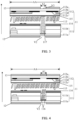
- FIG. 2A illustrates a schematic diagram of a structure of a display apparatus disclosed herein according to a first embodiment of the disclosure.
- FIG. 2B illustrates a schematic diagram of a structure of a display apparatus according to a second embodiment of the disclosure.
- the display apparatus comprises a display module 10 and a camera module 20.
- the camera module 20 is arranged within a display area AA of the display module 10, and it is disposed over a side of the display module 10 that is far from or distal to a light-emitting surface of the display module 10.
- the light transmission direction is from a bottom to a top (as illustrated by the bottom-to-top arrow in the figures), and the upper side of the display module 10 has the light-emitting surface, and the camera module 20 is disposed below the lower side of the display module 10 in the figures.
- the display area AA of the display apparatus comprises a light-incident region A1 that positionally corresponds to a lens of the camera module 20.
- the light-incident region A1 is configured to allow an environmental light (i.e. the light from an outside environment, such as from a top of the display apparatus) to pass therethrough so as to reach the lens of the camera module 20.
- the display apparatus further comprises other structures such as driving circuits, which can be arranged within a frame region defined by a frame of the display apparatus and can be disposed behind the frame to be thereby shielded.
- the display area AA of the display module 10 is referred to as an area that is surrounded by the frame region.
- the region outside the light-incident region A1 in the display area AA comprises a plurality of pixels, and it is configured such that at least two sides of the light-incident region A1 are next to the plurality of pixels.
- the light-incident region A1 that positionally corresponds to the lens of the camera module 20 is referred to as that an orthographic projection of the lens of the camera module 20 on the display module 10 and an orthographic projection of the light-incident region 10 on the display module 10 are exactly or substantially matched with each other in size and shape.
- the edge of the light-incident region A1 can slightly exceed the edge of the orthographic projection of the lens of the camera module 20 on the display module 10.
- the camera module 20 is arranged inside the display area AA of the display apparatus, thus differing from existing display apparatuses where the camera module 20 is typically arranged outside the display module 10, or the display module 10 is cut to arrange the camera module 20 within a groove thus formed that often has an irregular shape.
- an area occupied by the display area AA of the display module 10 can be relatively larger than that in existing display apparatuses, and as a result, the display apparatus can thus have a larger display screen relative to the whole device.
- the camera module 20 is disposed over a side of the display module 10 that is far from its light-emitting side, there is no need to conduct irregular-shaped cutting to the display module 10, therefore the problems of low manufacturing efficiency and low yield caused by conducting irregular-shape cutting to the display module 10 can be avoided.
- the display apparatus is particularly suitable for a liquid crystal display apparatus.
- the aforementioned display module 10 comprises a liquid crystal cell 11, and the display apparatus further comprises a backlight portion 30.
- the display module 10 is arranged at a light-emitting side of the backlight portion 30.
- a mounting hole V1 is configured within the backlight portion 30, and the camera module 20 is arranged inside the mounting hole V1.
- the backlight portion 30 can comprise a backlight source, which comprises a light-emitting component 31 and an optical film group 32.
- the light-emitting component 31 is arranged at a light-incident side of the optical film group 32, whereas the display module 10 is arranged at a light-emitting side of the optical film group 32.
- the mounting hole V1 is arranged to pass through the optical film group 32.
- the backlight source can be a side-entry backlight source or a straight-down backlight source. If a straight-down backlight source is adopted, the bottom side of the optical film group 32 is the light-incident side thereof, whereas the upper side of the optical film group 32 is the light-emitting side thereof.
- the optical film group 32 can comprise film layers such as a light-guiding plate, a light-diffusing film layer, and a prism.
- the light-guiding plate has a light-incident side and a light-emitting side, and the film layers including the light-diffusing film layer and the prism can be configured over the light-emitting side of the light-guiding plate.
- the light-incident side of the optical film group 32 is substantially the light-incident side of the light-guiding plate, and the top side of the optical film group 32 is the light-emitting side.
- an adhesive portion 22 having a composition of an adhesive glue is arranged between, to thereby bond, the camera module 20 and an inner wall of the mounting hole V1.
- the camera module 20 is thus mounted inside the mounting hole V1 through the adhesive portion 22.
- the adhesive portion 22 is non-transparent, and as a result, the backlight portion 30 will not leak lights at a location of the mounting hole V1 to thereby influence the shooting effect of the camera module 20.
- the adhesive portion 22 can comprise an adhesive glue of a dark color such as a black color or a brown color.
- a convex portion 21 is arranged at an end (i.e. the upper end shown in the figure) of the camera module 20 that faces the display module 10.
- the convex portion 21 extends towards a side wall of the mounting hole V1
- a first adhesive layer 23 is arranged between the convex portion 21 and the display module 10.
- the adhesive portion 22 is arranged at a side of the convex portion 21 that departs from the display module 10.
- the first adhesive layer 23 can comprise a double-sided adhesive.
- the convex portion 21 can be configured to be ring-shaped, as such, the area of the double-sided adhesive can be increased, and the stability of the connection between the camera module 20 and the display module 10 can be increased.
- the backlight portion 30 and the display module 10 can be assembled together at first.
- the camera module 20 can be disposed at a pre-set location and can be further assembled with the display module 10 by means of the first adhesive layer 23.
- a non-transparent adhesive glue can be instilled into a space between the camera module 20 and the side wall of the mounting hole V1 to thereby form the adhesive portion 22.
- the convex portion 21 is further configured to have an upper end thereof higher than an upper end of the lens of the camera module 20. More specifically, it can be configured such that the upper surface of the convex portion 21 has a relatively larger distance to the bottom surface of the display module 10 than the upper surface of the lens of the camera module 20. Such a configuration ensures that the lens of the camera module 20 and the display module 10 do not contact with each other, therefore avoiding the occurrence of wearing of the lens of the camera module 20.
- FIG. 2B illustrates a second mounting approach of the camera module 20.
- the backlight portion 30 further comprises a backboard 33.
- the backboard 33 is arranged at a side of the backlight portion 30 distal to the display module 10, and the mounting hole V1 is configured to pass through both the optical film group 32 and the backboard 33.
- a mounting component 40 is fixedly mounted onto the backboard 33, and one end of the camera module 20 that is far away from the display module 10 is fixedly attached with the mounting component 40.
- the backboard 33 and the mounting component 40 can both be made of a metal material, and the mounting component 40 can be fixedly mounted onto the backboard 33 by means of welding.
- the camera module 20 can be fixedly attached with the mounting component 40 by means of gluing.
- a convex portion 24 can also be arranged at the upper end of the camera module 20.
- the convex portion 24 can be further arranged at a surrounding area of the camera module 20.
- the upper end of the convex portion 24 is configured to be higher than the upper end of the lens of the camera module 20. As such, the lens of the camera module 20 will not be in contact with the display module 20 to thus preventing wearing of the lens from occurring.
- the convex portion 24 can also be attached with the display module 10 by means of gluing (such as by means of the first adhesive layer 23 in the embodiments shown in FIG. 2A ).
- the mounting approach of the camera module 20 inside the mounting hole V1 is not limited to the approaches as illustrated in FIG. 2A and FIG. 2B .
- the mounting approaches in FIG. 2A and FIG. 2B can be combined according to some embodiments where the aforementioned mounting component 40 illustrated in FIG. 2B can also be employed in the embodiment illustrated in FIG. 2A .
- the camera module 20 can be mounted to be assembled though both the adhesive portion 22 and the mounting component 40 at the same time, therefore the mounting effect can be improved.
- the display module 10 comprises the liquid crystal cell 11.
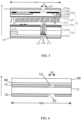
- the structure of the display module 10 will be described in detail with reference to FIG. 3, FIG. 4 , and FIG. 5 .
- the liquid crystal cell 11 comprises an array substrate 111 and an opposing substrate 112, which are arranged to face against each other.
- a liquid crystal layer 113 is arranged between the array substrate 111 and the opposing substrate 112.
- a first alignment layer 114 is configured between the array substrate 111 and the liquid crystal layer 113, and a second alignment layer 115 is configured between the opposing substrate 112 and the liquid crystal layer 113.
- the array substrate 111, the first alignment layer 114, the liquid crystal layer 113, the second alignment layer 115, and the opposing substrate 112 are sequentially stacked in the liquid crystal cell 11, as illustrated in a bottom-to-top direction in each of FIGS. 3-5 .
- the array substrate 111 can comprise a first base substrate 111a, and a display component layer 111b over the first base substrate 111a.
- the display component layer 111b is specifically arranged over a side of the first base substrate 111a that faces the liquid crystal layer 113.
- the display component layer 111b can comprise a film layer that is related to display.
- display component layer 111b can comprise a thin film transistor layer (including a gate electrode layer, a gate insulating layer, an active layer and a source-drain electrode layer, and so on), an inter-layer insulating layer, a passivation layer, and a planarization layer.
- the display component layer 111b is configured at a region outside the light-incident region A1.
- the opposing substrate 112 can comprise a second base substrate 112a, and can further comprise, over the second base substrate 112a, a light filter layer 112b, a black matrix 112c, and a transparent protection layer 112d.
- the transparent protection layer 112d can be configured to cover the whole display area AA.
- the light filter layer 112b and the black matrix 112c are both arranged between the transparent protection layer 112d and the second base substrate 112a.
- the light filter layer 112b and the black matrix 112c can be both arranged within a region of the display area AA outside the light-incident region A1, so that the camera module 20 can obtain images whose color is the same as the real color of the objects in the environment.
- FIGS. 3-5 respectively illustrates a structure of the display module 10 according to three embodiments of the disclosure (i.e. a first embodiment, a second embodiment, and a third embodiment, corresponding respectively to FIG. 3, FIG. 4 , and FIG. 5 ).
- the liquid crystal layer 113 is arranged at a region of the display area AA outside the light-incident region A1, whereas the first alignment layer 114 and the second alignment layer 115 are both configured to cover the whole display area AA.
- the liquid crystal layer 113 is configured to cover the whole display area AA, just as the first alignment layer 114 and the second alignment layer 115.
- the display module 10 can further comprise a driving electrode layer 116 that is arranged within the light-incident region A1.
- the driving electrode layer 116 is configured to generate an electric field in a portion of the liquid crystal layer 113 that positionally corresponds to the light-incident region A1.
- the electric field generated thereby can in turn drive the liquid crystal molecules of the portion of the liquid crystal layer 113 positionally corresponding to the light-incident region A1 to deflect, therefore adjusting an angle of lights that enter the lens of the camera module 20 to thereby realize zooming of the lens of the camera module 20.
- the driving electrode layer 116 can be arranged over the array substrate 111, over the opposing substrate 112, or partially over the array substrate 111 and partially over the opposing substrate 112.
- the display component layer 111b is arranged outside the light-incident region A1, within the light-incident region A1, it can be configured such that only the driving electrode layer 116, the first alignment layer 114, the second alignment layer 115, the liquid crystal layer 113, the transparent protection layer 112d, and signal lines (not shown in the figures) for providing signals to the driving electrode layer 116 are arranged between the first base substrate 111a and the second base substrate 112a.
- the display module 10 further comprises pixel electrodes and common electrodes in the display area AA, which can be arranged outside the light-incident region A1 to thereby generate electric fields for display outside the light-incident region A1.
- the electric field generated by the driving electrode layer 116 in the light-incident region A1 and the electric fields generated by the pixel electrodes and common electrodes at other regions of the display area AA are configured to be independent from each other, such that the zooming process for the camera module 20 and the displaying process of the display module 10 do not influence each other.
- a transparent spacer 117 is arranged between the array substrate 111 and the opposing substrate 112 within the light-incident region A1.
- the display module 10 further comprises a first polarizer 12 and a second polarizer 13.
- the second polarizer 12 is arranged over a side of the array substrate 111 that departs from the opposing substrate 112, and the second polarizer is arranged over a side of the opposing substrate 112 that departs from the array substrate 111. It is further configured such that a transmission axis of the fist polarizer 12 and a transmission axis of the second polarizer 13 are substantially perpendicular to each other.
- a cover plate 50 can be further arranged over a side of the second polarizer 13 that departs from the opposing substrate 112, and a second adhesive layer 60 is arranged between the cover plate 50 and the second polarizer 13.
- FIG. 6 and FIG. 7 respectively illustrate the bonding between the display module 10 and the cover plate 50 according to two embodiments of the disclosure.
- a light-transmissive opening V2 is arranged both in the first polarizer 12 at a position corresponding to the light-incident region A1 and in the second polarizer 13 at a position corresponding to the light-incident region A1.
- the polarization states do not change.
- the brightness of the lights will not be reduced, and thus the brightness of the lights received by the camera module 20 will be improved and the shooting effect will also be improved.
- one or both of the light-transmissive opening V2 in the first polarizer 12 and the light-transmissive opening V2 in the second polarizer 13 can be further filled with a transparent film layer 61.
- the light-transmissive opening V2 in the second polarizer 13 is filled with the transparent film layer 61. This configuration can prevent an air layer from being formed between the cover plate 50 and the opposing substrate 112. The air layer thus formed can negatively influence the shooting effect.
- the second adhesive layer 60 and the cover plate 50 can be first bonded together.
- the second polarizer 13 and the opposing substrate 112 can be bonded together, and the transparent film layer 61 can be filled into the light-transmissive opening V2.
- the cover plate 50 that is boned with the second adhesive layer 60 can be further bonded with the second polarizer 13 that is bonded with the opposing substrate 112.
- the transparent film layer 61 can comprise a transparent adhesive or comprise a film layer made of a solidified transparent liquid.
- the material of the transparent film layer 61 can be same as the material of the second adhesive layer 60.
- each of the first polarizer 12 and the second polarizer 13 can be configured to have a portion thereof that positionally corresponds to the light-incident region A1 is light-transmissive.
- each of the first polarizer 12 and the second polarizer 13 can have a light-transmissive portion (i.e. comprising a material that is integrated with other portions of the polarizer yet is transparent or light-transmissive) to thereby allow the environmental lights to pass therethrough to thereby be able to enter the lens of the camera module 20.
- a light-transmissive portion i.e. comprising a material that is integrated with other portions of the polarizer yet is transparent or light-transmissive
- a polarizer i.e. the first polarizer 12 or the second polarizer 13
- a laser processing can be conducted over a portion of the polarizer that positionally corresponds to the light-incident region A1, such that the portion of the polarizer does not change the polarization state of the lights.
- the camera module is still arranged in the display region of the display module.
- the area the display screen occupied in the display apparatus can be increased (in some example, the percentage of the display screen in the display apparatus can be more than 93%).
- the camera module is arranged over a side of the display module that is far away from its light-emitting side. Therefore there is no need to conduct irregular-shaped cutting over the display module, and in turn, the problems of low yield and low production efficiency caused by irregular- shaped cutting can thus be avoided.
- a driving electrode layer can be arranged within a region of the liquid crystal cell that positionally corresponds to the lens of the camera module.
- the driving electrode layer can drive the liquid crystal molecules to deflect, which can change the incident angle of the light entering the lens of the camera module, thereby realizing zooming of the lens of the camera module.
Landscapes
- Physics & Mathematics (AREA)
- Nonlinear Science (AREA)
- Mathematical Physics (AREA)
- Chemical & Material Sciences (AREA)
- Crystallography & Structural Chemistry (AREA)
- General Physics & Mathematics (AREA)
- Optics & Photonics (AREA)
- Devices For Indicating Variable Information By Combining Individual Elements (AREA)
- Liquid Crystal (AREA)
Description
- The present application claims priority to
Chinese Patent Application No. 201810385295.7 filed on April 26, 2018 - The present disclosure relates generally to a field of display technologies, and specifically to a display apparatus.
- Camera module is one of the important structures that is often integrated in display apparatuses such as laptops and mobile phones. Usually, the camera(s) in a camera modules is/are configured outside a display region of the display panel (i.e. display screen), and as a result, the area that is occupied by the display screen is reduced.
- At present time, in order to improve the area that the display screen occupies, some manufacturers have adopted a compartment design for arranging certain part of the display screen for camera modules and other part of the display screen for display region. Typically a region of a rectangular-shaped display screen is cut for arranging a camera module in the display apparatus, and an irregular-shaped display screen is thus obtained as a result.
- However, the manufacturing efficiency of this above irregular-shaped compartment design is relatively low, and problems and issues easily occur during the manufacturing process.
U.S. Patent ApplicationUS20160161664A1 is directed to reduce brightness unevenness at the periphery of a non-display region in a display device that uses an edge-type backlight by means of a display device being provided with a liquid crystal panel, a light guide plate, which has the surface opposing the liquid crystal panel as the light emitting surface and one lateral surface other than the light emitting surface and the surface opposite the light emitting surface as the light incident surface, a light source unit, which opposes the light incident surface, and an opening that pierces the light guide plate from the light emitting surface to the surface opposite the light emitting surface, the configuration being such that the length (X) from the light incident surface to the center of the opening is at least 1/2 the length (L) from the light incident surface to the lateral surface opposite the light incident surface. A display apparatus including the features defined in the preamble of appended claim 1 is further disclosed inUS 2016/161664 A1 . -
US 2014/104543 A1 aims at entirely integrating a conventional camera module into a liquid crystal display panel, such separate conventional camera modules typically including a light-detecting sensor chip and a conventional lens positioned in front of it for projecting images onto the light-detecting sensor chip.US 2014/104543 A1 therefore suggests integrating the sensor chip directly onto the TFT array substrate of the display panel and employing the liquid crystals situated between the colour filter substrate and the array substrate of the LCD panel to create a planar liquid crystal lens, so as to achieve the functions of a traditional lens (e.g., a plastic or glass lens). The liquid crystal lens inUS 2014/104543 A1 works in conjunction with the integrated chip on the array substrate to form a camera module (= sensor chip + LC lens), making the camera module (= sensor chip + LC lens) inUS 2014/104543 A1 an integrated part of the corresponding liquid crystal panel.US 2014/104543 A1 highlights the advantage of achieving an efficient optical zoom effect in a compact space, thanks to the lightweight and thin characteristics of the liquid crystal lens integrated into the LCD panel rendering a conventional lens of the camera module obsolete. - The present invention provides a display apparatus according to appended claim 1. Preferred embodiments of the display apparatus are defined in the appended dependent claims.
- To more clearly illustrate some of the embodiments, the following is a brief description of the drawings. The drawings in the following descriptions are only illustrative of some embodiments. For those of ordinary skill in the art, other drawings of other embodiments can become apparent based on these drawings.
-
FIG. 1 is a top view of a display apparatus according to some embodiments of the disclosure; -
FIG. 2A is a first structural diagram of the display apparatus provided by the present disclosure; -
FIG. 2B is a second structural diagram of the display apparatus provided by the present disclosure; -
FIG. 3 is a first structural diagram of the display module provided by the present disclosure; -
FIG 4 is a second structural diagram of the display module provided by the present disclosure; -
FIG. 5 is a third structural diagram of the display module provided by the present disclosure; -
FIG. 6 andFIG. 7 are diagrams respectively illustrating the two bonding states of the display module and the cover plate. - In the following, with reference to the drawings of the embodiments disclosed herein, the technical solutions of the embodiments of the invention will be described in a clear and fully understandable way.
- It is noted that the described embodiments are merely a portion but not all of the embodiments of the invention. Based on the described embodiments of the invention, those ordinarily skilled in the art can obtain other embodiment(s), which come(s) within the scope sought for protection by the invention.
- The purpose of this present disclosure is to provide a display apparatus wherein a camera module is arranged within, and integrated with, a display area of a display module (i.e. display screen).
-
FIG. 1 illustrates top view of a display apparatus according to some embodiments of the disclosure. As shown inFIG. 1 , the display apparatus comprises adisplay module 10 and acamera module 20. Thecamera module 20 is substantially arranged within a display area AA (shown by the rectangular shape in the figure) of thedisplay module 10. Importantly, in the display apparatus illustrated inFIG. 1 , the camera module 001 is integrated with the display module 002, as described below and illustrated inFIG. 2A and FIG. 2B . -
FIG. 2A illustrates a schematic diagram of a structure of a display apparatus disclosed herein according to a first embodiment of the disclosure.FIG. 2B illustrates a schematic diagram of a structure of a display apparatus according to a second embodiment of the disclosure. - As shown in both
FIG. 2A and FIG. 2B , the display apparatus comprises adisplay module 10 and acamera module 20. Thecamera module 20 is arranged within a display area AA of thedisplay module 10, and it is disposed over a side of thedisplay module 10 that is far from or distal to a light-emitting surface of thedisplay module 10. In the display apparatus as specifically illustrated in bothFIG. 2A and FIG. 2B , the light transmission direction is from a bottom to a top (as illustrated by the bottom-to-top arrow in the figures), and the upper side of thedisplay module 10 has the light-emitting surface, and thecamera module 20 is disposed below the lower side of thedisplay module 10 in the figures. - The display area AA of the display apparatus comprises a light-incident region A1 that positionally corresponds to a lens of the
camera module 20. The light-incident region A1 is configured to allow an environmental light (i.e. the light from an outside environment, such as from a top of the display apparatus) to pass therethrough so as to reach the lens of thecamera module 20. - Herein, it should be understood that the display apparatus further comprises other structures such as driving circuits, which can be arranged within a frame region defined by a frame of the display apparatus and can be disposed behind the frame to be thereby shielded. As such, the display area AA of the
display module 10 is referred to as an area that is surrounded by the frame region. - The region outside the light-incident region A1 in the display area AA comprises a plurality of pixels, and it is configured such that at least two sides of the light-incident region A1 are next to the plurality of pixels. It should be noted that the light-incident region A1 that positionally corresponds to the lens of the
camera module 20 is referred to as that an orthographic projection of the lens of thecamera module 20 on thedisplay module 10 and an orthographic projection of the light-incident region 10 on thedisplay module 10 are exactly or substantially matched with each other in size and shape. Herein, considering the manufacturing inaccuracy when assembling the display apparatus, the edge of the light-incident region A1 can slightly exceed the edge of the orthographic projection of the lens of thecamera module 20 on thedisplay module 10. - In the display apparatus disclosed herein, the
camera module 20 is arranged inside the display area AA of the display apparatus, thus differing from existing display apparatuses where thecamera module 20 is typically arranged outside thedisplay module 10, or thedisplay module 10 is cut to arrange thecamera module 20 within a groove thus formed that often has an irregular shape. - In the display apparatus disclosed herein, an area occupied by the display area AA of the
display module 10 can be relatively larger than that in existing display apparatuses, and as a result, the display apparatus can thus have a larger display screen relative to the whole device. - In addition, because the
camera module 20 is disposed over a side of thedisplay module 10 that is far from its light-emitting side, there is no need to conduct irregular-shaped cutting to thedisplay module 10, therefore the problems of low manufacturing efficiency and low yield caused by conducting irregular-shape cutting to thedisplay module 10 can be avoided. - In the present disclosure, the display apparatus is particularly suitable for a liquid crystal display apparatus. Accordingly, in the display apparatus, the
aforementioned display module 10 comprises aliquid crystal cell 11, and the display apparatus further comprises abacklight portion 30. Thedisplay module 10 is arranged at a light-emitting side of thebacklight portion 30. - In order to reduce a thickness of the display apparatus, as shown in both
FIG. 2A and FIG. 2B , a mounting hole V1 is configured within thebacklight portion 30, and thecamera module 20 is arranged inside the mounting hole V1. - Herein, the
backlight portion 30 can comprise a backlight source, which comprises a light-emittingcomponent 31 and anoptical film group 32. The light-emittingcomponent 31 is arranged at a light-incident side of theoptical film group 32, whereas thedisplay module 10 is arranged at a light-emitting side of theoptical film group 32. The mounting hole V1 is arranged to pass through theoptical film group 32. - Herein, the backlight source can be a side-entry backlight source or a straight-down backlight source. If a straight-down backlight source is adopted, the bottom side of the
optical film group 32 is the light-incident side thereof, whereas the upper side of theoptical film group 32 is the light-emitting side thereof. - If a side-entry backlight source is adopted, the
optical film group 32 can comprise film layers such as a light-guiding plate, a light-diffusing film layer, and a prism. The light-guiding plate has a light-incident side and a light-emitting side, and the film layers including the light-diffusing film layer and the prism can be configured over the light-emitting side of the light-guiding plate. As such, the light-incident side of theoptical film group 32 is substantially the light-incident side of the light-guiding plate, and the top side of theoptical film group 32 is the light-emitting side. - In the following, with reference to
FIG. 2A and FIG. 2B , mounting of thecamera module 20 inside the mounting hole V1 of the display apparatus will be described in detail. - According to a first mounting approach of the
camera module 20 shown inFIG. 2A , anadhesive portion 22 having a composition of an adhesive glue is arranged between, to thereby bond, thecamera module 20 and an inner wall of the mounting hole V1. Thecamera module 20 is thus mounted inside the mounting hole V1 through theadhesive portion 22. In some preferred embodiments, theadhesive portion 22 is non-transparent, and as a result, thebacklight portion 30 will not leak lights at a location of the mounting hole V1 to thereby influence the shooting effect of thecamera module 20. Herein, theadhesive portion 22 can comprise an adhesive glue of a dark color such as a black color or a brown color. - As further shown in
FIG. 2A , aconvex portion 21 is arranged at an end (i.e. the upper end shown in the figure) of thecamera module 20 that faces thedisplay module 10. Theconvex portion 21 extends towards a side wall of the mounting hole V1, a firstadhesive layer 23 is arranged between theconvex portion 21 and thedisplay module 10. Theadhesive portion 22 is arranged at a side of theconvex portion 21 that departs from thedisplay module 10. - Herein, the first
adhesive layer 23 can comprise a double-sided adhesive. Additionally, theconvex portion 21 can be configured to be ring-shaped, as such, the area of the double-sided adhesive can be increased, and the stability of the connection between thecamera module 20 and thedisplay module 10 can be increased. - During an assembling process of the display apparatus, the
backlight portion 30 and thedisplay module 10 can be assembled together at first. Next, thecamera module 20 can be disposed at a pre-set location and can be further assembled with thedisplay module 10 by means of the firstadhesive layer 23. Then a non-transparent adhesive glue can be instilled into a space between thecamera module 20 and the side wall of the mounting hole V1 to thereby form theadhesive portion 22. - During the above step of instilling the adhesive glue into the space between the
camera module 20 and the side wall of the mounting hole V1 to thereby form theadhesive portion 22, because of the presence of theconvex portion 21, the adhesive glue is prevented from flowing to a front end of the camera, and the shooting effect of thecamera module 20 can thus be ensured. - In addition, the
convex portion 21 is further configured to have an upper end thereof higher than an upper end of the lens of thecamera module 20. More specifically, it can be configured such that the upper surface of theconvex portion 21 has a relatively larger distance to the bottom surface of thedisplay module 10 than the upper surface of the lens of thecamera module 20. Such a configuration ensures that the lens of thecamera module 20 and thedisplay module 10 do not contact with each other, therefore avoiding the occurrence of wearing of the lens of thecamera module 20. -
FIG. 2B illustrates a second mounting approach of thecamera module 20. As shown in the figure, thebacklight portion 30 further comprises abackboard 33. The backboard 33 is arranged at a side of thebacklight portion 30 distal to thedisplay module 10, and the mounting hole V1 is configured to pass through both theoptical film group 32 and thebackboard 33. A mountingcomponent 40 is fixedly mounted onto the backboard 33, and one end of thecamera module 20 that is far away from thedisplay module 10 is fixedly attached with the mountingcomponent 40. - Herein, the
backboard 33 and the mountingcomponent 40 can both be made of a metal material, and the mountingcomponent 40 can be fixedly mounted onto the backboard 33 by means of welding. Thecamera module 20 can be fixedly attached with the mountingcomponent 40 by means of gluing. - Further specifically, a mounting slot that corresponds to the
camera module 20 can be configured on the mountingcomponent 40. A portion of thecamera module 20 can be configured to protrude beyond the backboard 33 along a direction that is away from thedisplay module 10 to thereby extend into the mounting slot. - Herein, in the embodiment illustrated in
FIG. 2B , aconvex portion 24 can also be arranged at the upper end of thecamera module 20. Theconvex portion 24 can be further arranged at a surrounding area of thecamera module 20. The upper end of theconvex portion 24 is configured to be higher than the upper end of the lens of thecamera module 20. As such, the lens of thecamera module 20 will not be in contact with thedisplay module 20 to thus preventing wearing of the lens from occurring. Theconvex portion 24 can also be attached with thedisplay module 10 by means of gluing (such as by means of the firstadhesive layer 23 in the embodiments shown inFIG. 2A ). - It should be noted that the mounting approach of the
camera module 20 inside the mounting hole V1 is not limited to the approaches as illustrated inFIG. 2A and FIG. 2B . For example, the mounting approaches inFIG. 2A and FIG. 2B can be combined according to some embodiments where theaforementioned mounting component 40 illustrated inFIG. 2B can also be employed in the embodiment illustrated inFIG. 2A . As such, thecamera module 20 can be mounted to be assembled though both theadhesive portion 22 and the mountingcomponent 40 at the same time, therefore the mounting effect can be improved. - As described above, the
display module 10 comprises theliquid crystal cell 11. In the following, the structure of thedisplay module 10 will be described in detail with reference toFIG. 3, FIG. 4 , andFIG. 5 . - The
liquid crystal cell 11 comprises anarray substrate 111 and an opposingsubstrate 112, which are arranged to face against each other. Aliquid crystal layer 113 is arranged between thearray substrate 111 and the opposingsubstrate 112. Afirst alignment layer 114 is configured between thearray substrate 111 and theliquid crystal layer 113, and asecond alignment layer 115 is configured between the opposingsubstrate 112 and theliquid crystal layer 113. In other words, thearray substrate 111, thefirst alignment layer 114, theliquid crystal layer 113, thesecond alignment layer 115, and the opposingsubstrate 112 are sequentially stacked in theliquid crystal cell 11, as illustrated in a bottom-to-top direction in each ofFIGS. 3-5 . - Herein, the
array substrate 111 can comprise afirst base substrate 111a, and adisplay component layer 111b over thefirst base substrate 111a. Thedisplay component layer 111b is specifically arranged over a side of thefirst base substrate 111a that faces theliquid crystal layer 113. - The
display component layer 111b can comprise a film layer that is related to display. Specifically,display component layer 111b can comprise a thin film transistor layer (including a gate electrode layer, a gate insulating layer, an active layer and a source-drain electrode layer, and so on), an inter-layer insulating layer, a passivation layer, and a planarization layer. In order to prevent thedisplay component layer 111b from influencing the strength of the light obtained by thecamera module 20, in some embodiments, as shown inFIG. 3, FIG. 4 andFIG. 5 , thedisplay component layer 111b is configured at a region outside the light-incident region A1. - The opposing
substrate 112 can comprise asecond base substrate 112a, and can further comprise, over thesecond base substrate 112a, alight filter layer 112b, ablack matrix 112c, and atransparent protection layer 112d. Thetransparent protection layer 112d can be configured to cover the whole display area AA. Thelight filter layer 112b and theblack matrix 112c are both arranged between thetransparent protection layer 112d and thesecond base substrate 112a. - According to some preferred embodiments of the display apparatus, the
light filter layer 112b and theblack matrix 112c can be both arranged within a region of the display area AA outside the light-incident region A1, so that thecamera module 20 can obtain images whose color is the same as the real color of the objects in the environment. -
FIGS. 3-5 respectively illustrates a structure of thedisplay module 10 according to three embodiments of the disclosure (i.e. a first embodiment, a second embodiment, and a third embodiment, corresponding respectively toFIG. 3, FIG. 4 , andFIG. 5 ). - In the first embodiment of the
display module 10 shown inFIG. 3 , theliquid crystal layer 113 is arranged at a region of the display area AA outside the light-incident region A1, whereas thefirst alignment layer 114 and thesecond alignment layer 115 are both configured to cover the whole display area AA. - In the second embodiment and the third embodiment of the
display module 10 as respectively shown inFIG. 4 andFIG. 5 , theliquid crystal layer 113 is configured to cover the whole display area AA, just as thefirst alignment layer 114 and thesecond alignment layer 115. - With reference to
FIG. 4 andFIG. 5 , in both the second embodiment and the third embodiment of thedisplay module 10, thedisplay module 10 can further comprise a drivingelectrode layer 116 that is arranged within the light-incident region A1. The drivingelectrode layer 116 is configured to generate an electric field in a portion of theliquid crystal layer 113 that positionally corresponds to the light-incident region A1. The electric field generated thereby can in turn drive the liquid crystal molecules of the portion of theliquid crystal layer 113 positionally corresponding to the light-incident region A1 to deflect, therefore adjusting an angle of lights that enter the lens of thecamera module 20 to thereby realize zooming of the lens of thecamera module 20. - Herein, depending on different embodiments of the disclosure, the driving
electrode layer 116 can be arranged over thearray substrate 111, over the opposingsubstrate 112, or partially over thearray substrate 111 and partially over the opposingsubstrate 112. - In the embodiments of the display apparatus where the
display component layer 111b is arranged outside the light-incident region A1, within the light-incident region A1, it can be configured such that only the drivingelectrode layer 116, thefirst alignment layer 114, thesecond alignment layer 115, theliquid crystal layer 113, thetransparent protection layer 112d, and signal lines (not shown in the figures) for providing signals to the drivingelectrode layer 116 are arranged between thefirst base substrate 111a and thesecond base substrate 112a. - The
display module 10 further comprises pixel electrodes and common electrodes in the display area AA, which can be arranged outside the light-incident region A1 to thereby generate electric fields for display outside the light-incident region A1. According to some embodiments, the electric field generated by the drivingelectrode layer 116 in the light-incident region A1 and the electric fields generated by the pixel electrodes and common electrodes at other regions of the display area AA are configured to be independent from each other, such that the zooming process for thecamera module 20 and the displaying process of thedisplay module 10 do not influence each other. - In addition, in order to maintain the thickness of the liquid crystal cell, in some embodiments shown in both
FIG. 3 andFIG. 5 , atransparent spacer 117 is arranged between thearray substrate 111 and the opposingsubstrate 112 within the light-incident region A1. - Further, as illustrated in
FIGS.1-5 , thedisplay module 10 further comprises afirst polarizer 12 and asecond polarizer 13. Thesecond polarizer 12 is arranged over a side of thearray substrate 111 that departs from the opposingsubstrate 112, and the second polarizer is arranged over a side of the opposingsubstrate 112 that departs from thearray substrate 111. It is further configured such that a transmission axis of thefist polarizer 12 and a transmission axis of thesecond polarizer 13 are substantially perpendicular to each other. - As further shown in
FIG. 2A and FIG. 2B , acover plate 50 can be further arranged over a side of thesecond polarizer 13 that departs from the opposingsubstrate 112, and a secondadhesive layer 60 is arranged between thecover plate 50 and thesecond polarizer 13. -
FIG. 6 andFIG. 7 respectively illustrate the bonding between thedisplay module 10 and thecover plate 50 according to two embodiments of the disclosure. In the embodiment shown inFIG. 6 , a light-transmissive opening V2 is arranged both in thefirst polarizer 12 at a position corresponding to the light-incident region A1 and in thesecond polarizer 13 at a position corresponding to the light-incident region A1. As such, when the lights from the environment pass through the light-transmissive opening V2 in thefirst polarizer 12 and the light-transmissive opening V2 in thesecond polarizer 13, the polarization states do not change. Thus the brightness of the lights will not be reduced, and thus the brightness of the lights received by thecamera module 20 will be improved and the shooting effect will also be improved. - Optionally, one or both of the light-transmissive opening V2 in the
first polarizer 12 and the light-transmissive opening V2 in thesecond polarizer 13 can be further filled with atransparent film layer 61. According to some preferred embodiments shown inFIGS. 1 ,2 and7 , the light-transmissive opening V2 in thesecond polarizer 13 is filled with thetransparent film layer 61. This configuration can prevent an air layer from being formed between thecover plate 50 and the opposingsubstrate 112. The air layer thus formed can negatively influence the shooting effect. - In the manufacturing process, the second
adhesive layer 60 and thecover plate 50 can be first bonded together. Next, thesecond polarizer 13 and the opposingsubstrate 112 can be bonded together, and thetransparent film layer 61 can be filled into the light-transmissive opening V2. Then, thecover plate 50 that is boned with the secondadhesive layer 60 can be further bonded with thesecond polarizer 13 that is bonded with the opposingsubstrate 112. - Herein, the
transparent film layer 61 can comprise a transparent adhesive or comprise a film layer made of a solidified transparent liquid. Specifically, the material of thetransparent film layer 61 can be same as the material of the secondadhesive layer 60. - It is noted that in addition to the above mentioned embodiments where a light-transmissive opening V2, filled with or without a
transparent film layer 61, is arranged in both thefirst polarizer 12 and thesecond polarizer 13 and at positions corresponding to the light-incident region A1 to thereby allow the lights from the outside environment to pass through thefirst polarizer 12 and thesecond polarizer 13 to ultimately enter the lens of thecamera module 20 without block, according to some other embodiments of the disclosure, each of thefirst polarizer 12 and thesecond polarizer 13 can be configured to have a portion thereof that positionally corresponds to the light-incident region A1 is light-transmissive. - In other words, instead of having a light-transmissive opening V2 (i.e. a though hole absent of the polarizer material), each of the
first polarizer 12 and thesecond polarizer 13 can have a light-transmissive portion (i.e. comprising a material that is integrated with other portions of the polarizer yet is transparent or light-transmissive) to thereby allow the environmental lights to pass therethrough to thereby be able to enter the lens of thecamera module 20. - In order to process the above structure, a polarizer (i.e. the
first polarizer 12 or the second polarizer 13) can be first disposed to cover the whole display area AA. Then, a laser processing can be conducted over a portion of the polarizer that positionally corresponds to the light-incident region A1, such that the portion of the polarizer does not change the polarization state of the lights. - In the display apparatus disclosed herein, the camera module is still arranged in the display region of the display module. As a result, the area the display screen occupied in the display apparatus can be increased (in some example, the percentage of the display screen in the display apparatus can be more than 93%).
- In addition, the camera module is arranged over a side of the display module that is far away from its light-emitting side. Therefore there is no need to conduct irregular-shaped cutting over the display module, and in turn, the problems of low yield and low production efficiency caused by irregular- shaped cutting can thus be avoided.
- Furthermore, a driving electrode layer can be arranged within a region of the liquid crystal cell that positionally corresponds to the lens of the camera module. The driving electrode layer can drive the liquid crystal molecules to deflect, which can change the incident angle of the light entering the lens of the camera module, thereby realizing zooming of the lens of the camera module.
- Although specific embodiments have been described above in detail, the description is merely for purposes of illustration. It should be appreciated, therefore, that many aspects described above are not intended as required or essential elements unless explicitly stated otherwise.
- Various modifications of the disclosed aspects of the exemplary embodiments, in addition to those described above, can be made by a person of ordinary skill in the art without departing from the scope of the invention defined in the following claims.
Claims (11)
- A display apparatus, comprising:a display module (10); anda camera module (20);wherein:the camera module (20) is within a display area (AA) of the display module (10);the camera module (20) is over a side of the display module (10) distal to a light-emitting surface of the display module (10); andthe display area (AA) of the display module (10) comprises a light-incident region (A1) positionally corresponding to a lens of the camera module (20), wherein the light-incident region (A1) is configured to allow light from a side of the display apparatus proximal to the light-emitting surface of the display module (10) to pass therethrough to thereby enter the lens of the camera module (20), andwherein the display module (10) comprises a liquid crystal cell (11), the liquid crystal cell (11) comprises an array substrate (111), a liquid crystal layer (113), and an opposing substrate (112), sequentially stacked over one another along a direction of light transmission,the liquid crystal layer (113) covers the light-incident region (A1),the display module (10) further comprises a driving electrode layer (116) at a position of the liquid crystal cell (11) corresponding to the light-incident region (A1),the driving electrode layer (116) is configured to generate an electric field in a portion of the liquid crystal layer (113) positionally corresponding to the light-incident region (A1) to drive liquid crystal molecules in said portion of the liquid crystal layer (113) to deflect, the electric field generated by the driving electrode layer (116) being independent from any of electric fields generated in portions of the liquid crystal layer (113) positionally corresponding to regions of the display area (AA) otherthan the light-incident region (A1), characterized in that the electric field generated by said electrode layer (16) in said portion of the liquid crystal layer (113) positionally corresponding to the light-incident region (A1) is configured to adjust an incidence angle of light that enters the lens of the camera module (20) to realize zooming of the lens of the camera module (20).
- The display apparatus of Claim 1, further comprising a backlight portion (30) over a side of the display module (10) distal to the light-emitting surface of the display module (10), wherein:
the camera module (20) is inside a mounting hole in the backlight portion (30). - The display apparatus of Claim 2, wherein the camera module (20) further comprises a convex portion (21, 24) at an end of the camera module facing the display module (10), wherein the convex portion (21, 24) is configured to ensure that the lens of the camera module (20) has a distance to the display module (10), the convex portion (21, 24) comprises a ring having an opening thereof positionally corresponding to the lens of the camera module (20), wherein the opening is configured to allow the light passing through the light-incident region (A1) of the display module (10) to pass therethrough to thereby enter the lens of the camera module (20).
- The display apparatus of Claim 2, further comprising an adhesive portion (22) between the camera module (20) and a side wall of the mounting hole (V1), the adhesive portion (22) is non-light-transmissive.
- The display apparatus of Claim 3, further comprising a first adhesive layer (23) between the convex portion (21, 24) and the display module (10).
- The display apparatus of Claim 2, wherein the backlight portion (30) comprises:a backboard (33) over a side thereof distal to the display module (10); anda mounting component (40) fixedly attached onto the backboard (33);wherein:the mounting component (40) is configured to fixedly mount the camera module (20) with the display module (10) by attaching an end portion of the camera module (20) distal to the lens, the mounting component (40) is provided with a mounting slot at a surface thereof proximal to the display module (10), wherein:
the mounting hole (V1) passes through the backboard (33); and
the end portion of the camera module (20) extends into the mounting slot to attach with the mounting component (40). - The display apparatus of Claim 1, wherein the display module (10) further comprises:a first alignment layer (114) between the array substrate (111) and the liquid crystal layer (113); anda second alignment layer (115) between the opposing substrate (112) and the liquid crystal layer (113).
- The display apparatus of Claim 1, wherein the liquid crystal cell (11) further comprises a transparent spacer (117) between the array substrate (111) and the opposing substrate (112), wherein:
the transparent spacer (117) is arranged to positionally correspond to the light-incident region (A1). - The display apparatus of Claim 1, wherein the liquid crystal cell (11) further comprises a transparent spacer (117) between the array substrate (111) and the opposing substrate (112), wherein:
the transparent spacer (117) is absent in the light-incident region (A1). - The display apparatus of Claim 1, wherein the liquid crystal cell (11) further comprises:a first polarizer (12) over a side of the array substrate (111) distal to the opposing substrate (112); anda second polarizer (13) over a side of the opposing substrate (112) distal to the array substrate (111);wherein:the first polarizer (12) is provided with a first light-transmissive window at a position thereof corresponding to the light-incident region (A1); andthe second polarizer (13) is provided with a second light-transmissive window at a position thereof corresponding to the light-incident region (A1).
- The display apparatus of Claim 10, wherein at least one of the first light-transmissive window and the second light-transmissive window comprises a light-transmissive opening (V2), or at least one of the first light-transmissive window and the second light-transmissive window comprises a light-transmissive material.
Applications Claiming Priority (2)
| Application Number | Priority Date | Filing Date | Title |
|---|---|---|---|
| CN201810385295.7A CN108594524B (en) | 2018-04-26 | 2018-04-26 | display device |
| PCT/CN2018/118139 WO2019205627A1 (en) | 2018-04-26 | 2018-11-29 | Display apparatus |
Publications (3)
| Publication Number | Publication Date |
|---|---|
| EP3785073A1 EP3785073A1 (en) | 2021-03-03 |
| EP3785073A4 EP3785073A4 (en) | 2022-02-23 |
| EP3785073B1 true EP3785073B1 (en) | 2025-04-23 |
Family
ID=63610109
Family Applications (1)
| Application Number | Title | Priority Date | Filing Date |
|---|---|---|---|
| EP18857398.4A Active EP3785073B1 (en) | 2018-04-26 | 2018-11-29 | Display apparatus |
Country Status (4)
| Country | Link |
|---|---|
| US (1) | US10690959B2 (en) |
| EP (1) | EP3785073B1 (en) |
| CN (1) | CN108594524B (en) |
| WO (1) | WO2019205627A1 (en) |
Families Citing this family (78)
| Publication number | Priority date | Publication date | Assignee | Title |
|---|---|---|---|---|
| CN108196388B (en) * | 2018-02-12 | 2022-04-19 | 京东方科技集团股份有限公司 | Display device and manufacturing method thereof |
| CN108594524B (en) * | 2018-04-26 | 2021-04-13 | 京东方科技集团股份有限公司 | display device |
| CN109100891A (en) * | 2018-08-10 | 2018-12-28 | 厦门天马微电子有限公司 | A kind of display panel and display device |
| CN109143648B (en) * | 2018-09-28 | 2021-10-08 | 上海中航光电子有限公司 | Display panel and display device |
| CN109218475B (en) * | 2018-09-30 | 2021-09-24 | 厦门天马微电子有限公司 | Display device |
| CN109147595B (en) * | 2018-09-30 | 2021-04-02 | 厦门天马微电子有限公司 | Display device and manufacturing method thereof |
| CN110971722B (en) * | 2018-09-30 | 2021-07-13 | 北京小米移动软件有限公司 | Image capturing method and device |
| TWI693452B (en) * | 2018-10-04 | 2020-05-11 | 友達光電股份有限公司 | Liquid crystal device |
| CN109494241B (en) * | 2018-10-08 | 2020-11-24 | 武汉华星光电半导体显示技术有限公司 | Flexible OLED display panel and preparation method thereof |
| CN109407375B (en) * | 2018-10-16 | 2021-10-15 | Oppo广东移动通信有限公司 | A display panel and its manufacturing method, display panel assembly, and electronic equipment |
| US10976615B2 (en) | 2018-10-30 | 2021-04-13 | Wuhan China Star Optoelectronics Technology Co., Ltd. | Liquid crystal display panel and manufacturing method thereof |
| CN109343253A (en) * | 2018-10-30 | 2019-02-15 | 武汉华星光电技术有限公司 | Liquid crystal display panel and preparation method thereof |
| CN109343285B (en) * | 2018-10-31 | 2021-08-13 | 厦门天马微电子有限公司 | Display panels and display devices |
| CN109307962B (en) * | 2018-11-13 | 2021-08-03 | 华为技术有限公司 | A liquid crystal display panel, liquid crystal display screen and electronic equipment |
| WO2020097785A1 (en) * | 2018-11-13 | 2020-05-22 | 华为技术有限公司 | Screen assembly and terminal device |
| JP7160643B2 (en) | 2018-11-16 | 2022-10-25 | 株式会社ジャパンディスプレイ | Display device |
| CN109358451B (en) * | 2018-11-28 | 2020-10-13 | 武汉华星光电技术有限公司 | Backlight module and display device thereof |
| CN210465916U (en) * | 2018-12-03 | 2020-05-05 | 鸿富锦精密工业(深圳)有限公司 | Liquid crystal display device having a plurality of pixel electrodes |
| CN110618549B (en) * | 2018-12-03 | 2024-10-29 | 鸿富锦精密工业(深圳)有限公司 | Display device |
| CN110955079A (en) * | 2018-12-03 | 2020-04-03 | 鸿富锦精密工业(深圳)有限公司 | Liquid crystal display device having a plurality of pixel electrodes |
| CN111258113A (en) * | 2018-12-03 | 2020-06-09 | 鸿富锦精密工业(深圳)有限公司 | Liquid crystal display device |
| USD912057S1 (en) | 2018-12-04 | 2021-03-02 | Hon Hai Precision Industry Co., Ltd. | Display module |
| CN110888261A (en) * | 2018-12-07 | 2020-03-17 | 鸿富锦精密工业(深圳)有限公司 | Display panel and display device |
| CN211180468U (en) * | 2018-12-07 | 2020-08-04 | 鸿富锦精密工业(深圳)有限公司 | Display panel and display device |
| CN109669291B (en) * | 2018-12-11 | 2022-01-14 | 厦门天马微电子有限公司 | Display panel and display device |
| CN109541833A (en) * | 2018-12-13 | 2019-03-29 | 华为技术有限公司 | Display component, display device and its driving method |
| KR102612738B1 (en) * | 2018-12-18 | 2023-12-12 | 엘지디스플레이 주식회사 | Display device |
| KR102680693B1 (en) * | 2018-12-18 | 2024-07-01 | 엘지디스플레이 주식회사 | Display device |
| CN109407198B (en) * | 2018-12-19 | 2020-09-01 | 武汉华星光电技术有限公司 | Polaroid and display panel |
| US11290628B2 (en) * | 2018-12-27 | 2022-03-29 | Dynascan Technology Corp. | Display apparatus |
| CN109561183A (en) * | 2019-01-03 | 2019-04-02 | 京东方科技集团股份有限公司 | Display screen module and mobile terminal |
| CN111491077B (en) * | 2019-01-29 | 2022-09-16 | 北京小米移动软件有限公司 | Terminal, display panel, image acquisition module and display control method |
| CN109817090B (en) * | 2019-01-30 | 2021-12-10 | 京东方科技集团股份有限公司 | Display device and method for manufacturing display device |
| CN111508337A (en) * | 2019-01-31 | 2020-08-07 | 北京小米移动软件有限公司 | Display panel, method of making the same, and display device |
| CN109637378A (en) * | 2019-01-31 | 2019-04-16 | 厦门天马微电子有限公司 | Display device and preparation method thereof |
| CN111508350B (en) * | 2019-01-31 | 2025-11-04 | 北京小米移动软件有限公司 | Display panel, its manufacturing method, and display device |
| CN109671359B (en) * | 2019-02-28 | 2020-11-20 | 厦门天马微电子有限公司 | Display device and method for manufacturing the same |
| CN109860266A (en) * | 2019-03-12 | 2019-06-07 | 武汉华星光电半导体显示技术有限公司 | A display panel and display device |
| JP2020148942A (en) * | 2019-03-14 | 2020-09-17 | シャープ株式会社 | Image display device |
| CN210605285U (en) * | 2019-03-26 | 2020-05-22 | 武汉华星光电技术有限公司 | Display panel and display device |
| CN110034128B (en) * | 2019-03-27 | 2021-07-23 | 武汉华星光电半导体显示技术有限公司 | Display device and driving method thereof |
| CN110045452A (en) * | 2019-03-28 | 2019-07-23 | 武汉华星光电技术有限公司 | Light guide plate, backlight module and display device |
| CN109856850B (en) * | 2019-03-29 | 2020-10-13 | 武汉华星光电技术有限公司 | Display device |
| CN109946885A (en) * | 2019-04-17 | 2019-06-28 | 武汉华星光电技术有限公司 | Liquid crystal display panel and electronic equipment |
| KR102651701B1 (en) * | 2019-04-23 | 2024-03-28 | 삼성전자주식회사 | A hole display and an electronic device including same |
| CN110187567A (en) * | 2019-05-15 | 2019-08-30 | 厦门天马微电子有限公司 | A kind of display panel and display device |
| CN110208891A (en) * | 2019-05-21 | 2019-09-06 | 华为技术有限公司 | A kind of polaroid, display screen and mobile terminal |
| CN112014989A (en) | 2019-05-31 | 2020-12-01 | 北京小米移动软件有限公司 | Display module, display device, display device control method and storage medium |
| CN110208976A (en) * | 2019-06-13 | 2019-09-06 | 信利光电股份有限公司 | A kind of full screen display mould group |
| CN110244483A (en) * | 2019-06-17 | 2019-09-17 | 武汉华星光电技术有限公司 | Array substrate and liquid crystal display panel |
| CN110346970A (en) * | 2019-06-18 | 2019-10-18 | 武汉华星光电技术有限公司 | Backlight module and display device |
| CN110133788B (en) * | 2019-06-24 | 2022-02-08 | 厦门天马微电子有限公司 | Polaroid, display panel and display device |
| CN113939751B (en) * | 2019-06-28 | 2024-09-27 | 住友化学株式会社 | Optical laminate |
| CN110441958A (en) * | 2019-07-05 | 2019-11-12 | 武汉华星光电技术有限公司 | A kind of display surface template die group |
| CN110335890A (en) | 2019-07-11 | 2019-10-15 | 京东方科技集团股份有限公司 | A kind of display panel and preparation method thereof, display device |
| CN110426895A (en) * | 2019-07-23 | 2019-11-08 | 武汉华星光电技术有限公司 | The production method of backlight module, display device and backlight module |
| CN111367108B (en) * | 2019-07-30 | 2023-07-25 | 友达光电股份有限公司 | Electronic device and manufacturing method thereof |
| US11476441B2 (en) | 2019-08-12 | 2022-10-18 | Beijing Boe Technology Development Co., Ltd. | Display apparatus and method of fabricating display apparatus |
| CN110609419A (en) * | 2019-08-23 | 2019-12-24 | 武汉华星光电技术有限公司 | Display panel preparation method and display panel |
| US10996503B2 (en) | 2019-09-24 | 2021-05-04 | Wuhan China Star Optoelectronics Technology Co., Ltd. | Display device and method of manufacturing same |
| CN110703486B (en) * | 2019-09-24 | 2021-04-27 | 武汉华星光电技术有限公司 | Display device and method of manufacturing the same |
| CN110632802B (en) * | 2019-09-25 | 2021-02-23 | 武汉华星光电技术有限公司 | Array substrate, display panel and manufacturing method of array substrate |
| CN110673371B (en) * | 2019-09-29 | 2021-07-20 | 维沃移动通信(杭州)有限公司 | Electronic device, control method thereof, and computer-readable storage medium |
| CN110780375B (en) * | 2019-11-15 | 2022-07-22 | 京东方科技集团股份有限公司 | Polaroid and preparation method thereof, display panel and display device |
| CN111031153B (en) * | 2019-11-21 | 2021-04-27 | 武汉华星光电半导体显示技术有限公司 | display module |
| CN110867136B (en) * | 2019-11-22 | 2021-10-15 | 维沃移动通信有限公司 | Pole screen and electronic equipment |
| CN111025752A (en) * | 2019-12-13 | 2020-04-17 | 武汉华星光电技术有限公司 | Display device and method for manufacturing the same |
| KR102749504B1 (en) * | 2019-12-31 | 2025-01-03 | 삼성디스플레이 주식회사 | Display device and Method for manufacturing a display device |
| CN111176018A (en) * | 2020-02-12 | 2020-05-19 | 武汉华星光电技术有限公司 | a display device |
| KR20210154316A (en) * | 2020-06-11 | 2021-12-21 | 삼성디스플레이 주식회사 | Electronic device and manufacturing method of the same |
| CN111766735B (en) * | 2020-06-18 | 2023-05-02 | 上海中航光电子有限公司 | Display panel and display device |
| CN111929759B (en) * | 2020-08-14 | 2022-06-07 | Oppo(重庆)智能科技有限公司 | Display screen, polaroid and electronic device |
| CN112015008A (en) * | 2020-09-15 | 2020-12-01 | 武汉华星光电技术有限公司 | Backlight module, liquid crystal display panel and manufacturing method of liquid crystal display panel |
| WO2022098058A1 (en) | 2020-11-06 | 2022-05-12 | 삼성전자 주식회사 | Electronic device including display |
| CN113593414B (en) * | 2021-07-30 | 2023-09-29 | 京东方科技集团股份有限公司 | Display panels and display devices |
| CN114089557B (en) * | 2021-11-29 | 2023-12-08 | 武汉华星光电技术有限公司 | Display device |
| CN115685617B (en) * | 2022-11-07 | 2024-02-20 | 武汉华星光电技术有限公司 | display device |
| CN116027583A (en) * | 2023-02-09 | 2023-04-28 | 业成科技(成都)有限公司 | Display panel, manufacturing method thereof, display device, electronic device |
Citations (1)
| Publication number | Priority date | Publication date | Assignee | Title |
|---|---|---|---|---|
| US20140104543A1 (en) * | 2012-10-11 | 2014-04-17 | Boe Technology Group Co., Ltd. | Method for integrating camera on liquid crsytal panel, liquid crystal panel and liquid-crystal display device |
Family Cites Families (14)
| Publication number | Priority date | Publication date | Assignee | Title |
|---|---|---|---|---|
| WO2000079338A1 (en) * | 1999-06-23 | 2000-12-28 | Citizen Watch Co., Ltd. | Liquid crystal display |
| US9143668B2 (en) * | 2010-10-29 | 2015-09-22 | Apple Inc. | Camera lens structures and display structures for electronic devices |
| KR102006775B1 (en) * | 2012-08-30 | 2019-08-02 | 엘지디스플레이 주식회사 | Liquid crystal panel and liquid crystal display device using the same |
| WO2015022887A1 (en) * | 2013-08-12 | 2015-02-19 | シャープ株式会社 | Display device |
| KR20150106232A (en) * | 2014-03-11 | 2015-09-21 | 삼성전자주식회사 | A touch recognition device and display applying the same |
| KR102384068B1 (en) * | 2015-09-11 | 2022-04-07 | 삼성디스플레이 주식회사 | Liquid Crystal Display |
| KR102501111B1 (en) * | 2015-12-28 | 2023-02-16 | 엘지디스플레이 주식회사 | Camera module integrated liquid display device and manufacturing method thereof |
| JP6665314B2 (en) * | 2016-11-07 | 2020-03-13 | 京セラ株式会社 | Image display device |
| KR102342609B1 (en) * | 2017-04-25 | 2021-12-22 | 후아웨이 테크놀러지 컴퍼니 리미티드 | Lcd display screen, electronic device, manufacturing method for lcd display screen |
| CN106973212B (en) * | 2017-05-18 | 2020-03-06 | 维沃移动通信有限公司 | Camera device and mobile terminal |
| CN107272242B (en) * | 2017-07-28 | 2020-09-29 | 维沃移动通信有限公司 | Display screen manufacturing method and display screen |
| CN207264062U (en) * | 2017-09-26 | 2018-04-20 | 昆山龙腾光电有限公司 | Display device |
| JP2019184828A (en) * | 2018-04-10 | 2019-10-24 | シャープ株式会社 | Liquid crystal display device |
| CN108594524B (en) * | 2018-04-26 | 2021-04-13 | 京东方科技集团股份有限公司 | display device |
-
2018
- 2018-04-26 CN CN201810385295.7A patent/CN108594524B/en active Active
- 2018-11-29 WO PCT/CN2018/118139 patent/WO2019205627A1/en not_active Ceased
- 2018-11-29 US US16/333,972 patent/US10690959B2/en active Active
- 2018-11-29 EP EP18857398.4A patent/EP3785073B1/en active Active
Patent Citations (1)
| Publication number | Priority date | Publication date | Assignee | Title |
|---|---|---|---|---|
| US20140104543A1 (en) * | 2012-10-11 | 2014-04-17 | Boe Technology Group Co., Ltd. | Method for integrating camera on liquid crsytal panel, liquid crystal panel and liquid-crystal display device |
Also Published As
| Publication number | Publication date |
|---|---|
| CN108594524B (en) | 2021-04-13 |
| CN108594524A (en) | 2018-09-28 |
| EP3785073A1 (en) | 2021-03-03 |
| US10690959B2 (en) | 2020-06-23 |
| EP3785073A4 (en) | 2022-02-23 |
| US20190331960A1 (en) | 2019-10-31 |
| WO2019205627A1 (en) | 2019-10-31 |
Similar Documents
| Publication | Publication Date | Title |
|---|---|---|
| US10690959B2 (en) | Display apparatus | |
| TWI719738B (en) | Display panel and display device using same | |
| US11796875B2 (en) | Display assembly, display device and driving method therefor | |
| US8134675B2 (en) | Liquid crystal display device | |
| EP2527911B1 (en) | Display | |
| CN101641634B (en) | Liquid crystal display panel with microlens array and method for manufacturing the same | |
| US11556024B2 (en) | Display assembly of electronic device, electronic device, and method for manufacturing display assembly | |
| US20200174307A1 (en) | Liquid crystal display device having high screen ratio | |
| KR101741821B1 (en) | Liquid crystal display device | |
| US20200174310A1 (en) | Liquid crystal display device | |
| KR20160000915A (en) | Display device | |
| US9817260B2 (en) | Display device and method of fabricating the same | |
| EP3336915B1 (en) | Display device | |
| US20120287352A1 (en) | Lighting device, display device and television receiver | |
| TWI687740B (en) | Thin film transistor driving circuit and liquid crystal display device | |
| US11451651B2 (en) | Display assembly of electronic device and electronic device | |
| JP2014174540A (en) | Liquid crystal display device | |
| EP4517412A1 (en) | Display panel and electronic equipment | |
| KR102622046B1 (en) | Display device | |
| KR102065031B1 (en) | Display apparatus having camera module | |
| KR101966863B1 (en) | Display device and method for manufacturing the same | |
| US10969621B2 (en) | Display assembly and display device | |
| KR101402152B1 (en) | Liquid crystal display device | |
| US20100053031A1 (en) | Electro-optical device and electronic apparatus | |
| US20250216718A1 (en) | Display device |
Legal Events
| Date | Code | Title | Description |
|---|---|---|---|
| STAA | Information on the status of an ep patent application or granted ep patent |
Free format text: STATUS: UNKNOWN |
|
| STAA | Information on the status of an ep patent application or granted ep patent |
Free format text: STATUS: THE INTERNATIONAL PUBLICATION HAS BEEN MADE |
|
| PUAI | Public reference made under article 153(3) epc to a published international application that has entered the european phase |
Free format text: ORIGINAL CODE: 0009012 |
|
| STAA | Information on the status of an ep patent application or granted ep patent |
Free format text: STATUS: REQUEST FOR EXAMINATION WAS MADE |
|
| 17P | Request for examination filed |
Effective date: 20190326 |
|
| AK | Designated contracting states |
Kind code of ref document: A1 Designated state(s): AL AT BE BG CH CY CZ DE DK EE ES FI FR GB GR HR HU IE IS IT LI LT LU LV MC MK MT NL NO PL PT RO RS SE SI SK SM TR |
|
| AX | Request for extension of the european patent |
Extension state: BA ME |
|
| DAV | Request for validation of the european patent (deleted) | ||
| DAX | Request for extension of the european patent (deleted) | ||
| A4 | Supplementary search report drawn up and despatched |
Effective date: 20220124 |
|
| RIC1 | Information provided on ipc code assigned before grant |
Ipc: G02F 1/1335 20060101ALI20220118BHEP Ipc: G02F 1/13357 20060101AFI20220118BHEP |
|
| REG | Reference to a national code |
Ref country code: DE Ref legal event code: R079 Free format text: PREVIOUS MAIN CLASS: G02F0001133570 Ipc: G02F0001133000 Ref document number: 602018081382 Country of ref document: DE |
|
| RIC1 | Information provided on ipc code assigned before grant |
Ipc: G02F 1/1335 20060101ALI20241217BHEP Ipc: G02F 1/1333 20060101ALI20241217BHEP Ipc: G02F 1/13357 20060101ALI20241217BHEP Ipc: G02F 1/133 20060101AFI20241217BHEP |
|
| GRAP | Despatch of communication of intention to grant a patent |
Free format text: ORIGINAL CODE: EPIDOSNIGR1 |
|
| STAA | Information on the status of an ep patent application or granted ep patent |
Free format text: STATUS: GRANT OF PATENT IS INTENDED |
|
| INTG | Intention to grant announced |
Effective date: 20250130 |
|
| GRAS | Grant fee paid |
Free format text: ORIGINAL CODE: EPIDOSNIGR3 |
|
| GRAA | (expected) grant |
Free format text: ORIGINAL CODE: 0009210 |
|
| STAA | Information on the status of an ep patent application or granted ep patent |
Free format text: STATUS: THE PATENT HAS BEEN GRANTED |
|
| AK | Designated contracting states |
Kind code of ref document: B1 Designated state(s): AL AT BE BG CH CY CZ DE DK EE ES FI FR GB GR HR HU IE IS IT LI LT LU LV MC MK MT NL NO PL PT RO RS SE SI SK SM TR |
|
| REG | Reference to a national code |
Ref country code: GB Ref legal event code: FG4D |
|
| REG | Reference to a national code |
Ref country code: CH Ref legal event code: EP |
|
| REG | Reference to a national code |
Ref country code: DE Ref legal event code: R096 Ref document number: 602018081382 Country of ref document: DE |
|
| REG | Reference to a national code |
Ref country code: IE Ref legal event code: FG4D |
|
| REG | Reference to a national code |
Ref country code: NL Ref legal event code: MP Effective date: 20250423 |
|
| PG25 | Lapsed in a contracting state [announced via postgrant information from national office to epo] |
Ref country code: NL Free format text: LAPSE BECAUSE OF FAILURE TO SUBMIT A TRANSLATION OF THE DESCRIPTION OR TO PAY THE FEE WITHIN THE PRESCRIBED TIME-LIMIT Effective date: 20250423 |
|
| REG | Reference to a national code |
Ref country code: AT Ref legal event code: MK05 Ref document number: 1788304 Country of ref document: AT Kind code of ref document: T Effective date: 20250423 |
|
| PG25 | Lapsed in a contracting state [announced via postgrant information from national office to epo] |
Ref country code: FI Free format text: LAPSE BECAUSE OF FAILURE TO SUBMIT A TRANSLATION OF THE DESCRIPTION OR TO PAY THE FEE WITHIN THE PRESCRIBED TIME-LIMIT Effective date: 20250423 Ref country code: ES Free format text: LAPSE BECAUSE OF FAILURE TO SUBMIT A TRANSLATION OF THE DESCRIPTION OR TO PAY THE FEE WITHIN THE PRESCRIBED TIME-LIMIT Effective date: 20250423 Ref country code: PT Free format text: LAPSE BECAUSE OF FAILURE TO SUBMIT A TRANSLATION OF THE DESCRIPTION OR TO PAY THE FEE WITHIN THE PRESCRIBED TIME-LIMIT Effective date: 20250825 |
|
| REG | Reference to a national code |
Ref country code: LT Ref legal event code: MG9D |
|
| PG25 | Lapsed in a contracting state [announced via postgrant information from national office to epo] |
Ref country code: GR Free format text: LAPSE BECAUSE OF FAILURE TO SUBMIT A TRANSLATION OF THE DESCRIPTION OR TO PAY THE FEE WITHIN THE PRESCRIBED TIME-LIMIT Effective date: 20250724 Ref country code: NO Free format text: LAPSE BECAUSE OF FAILURE TO SUBMIT A TRANSLATION OF THE DESCRIPTION OR TO PAY THE FEE WITHIN THE PRESCRIBED TIME-LIMIT Effective date: 20250723 |
|
| PG25 | Lapsed in a contracting state [announced via postgrant information from national office to epo] |
Ref country code: PL Free format text: LAPSE BECAUSE OF FAILURE TO SUBMIT A TRANSLATION OF THE DESCRIPTION OR TO PAY THE FEE WITHIN THE PRESCRIBED TIME-LIMIT Effective date: 20250423 |
|
| PG25 | Lapsed in a contracting state [announced via postgrant information from national office to epo] |
Ref country code: BG Free format text: LAPSE BECAUSE OF FAILURE TO SUBMIT A TRANSLATION OF THE DESCRIPTION OR TO PAY THE FEE WITHIN THE PRESCRIBED TIME-LIMIT Effective date: 20250423 |
|
| PG25 | Lapsed in a contracting state [announced via postgrant information from national office to epo] |
Ref country code: HR Free format text: LAPSE BECAUSE OF FAILURE TO SUBMIT A TRANSLATION OF THE DESCRIPTION OR TO PAY THE FEE WITHIN THE PRESCRIBED TIME-LIMIT Effective date: 20250423 |
|
| PG25 | Lapsed in a contracting state [announced via postgrant information from national office to epo] |
Ref country code: AT Free format text: LAPSE BECAUSE OF FAILURE TO SUBMIT A TRANSLATION OF THE DESCRIPTION OR TO PAY THE FEE WITHIN THE PRESCRIBED TIME-LIMIT Effective date: 20250423 |
|
| PG25 | Lapsed in a contracting state [announced via postgrant information from national office to epo] |
Ref country code: RS Free format text: LAPSE BECAUSE OF FAILURE TO SUBMIT A TRANSLATION OF THE DESCRIPTION OR TO PAY THE FEE WITHIN THE PRESCRIBED TIME-LIMIT Effective date: 20250723 |
|
| PG25 | Lapsed in a contracting state [announced via postgrant information from national office to epo] |
Ref country code: IS Free format text: LAPSE BECAUSE OF FAILURE TO SUBMIT A TRANSLATION OF THE DESCRIPTION OR TO PAY THE FEE WITHIN THE PRESCRIBED TIME-LIMIT Effective date: 20250823 |
|
| PG25 | Lapsed in a contracting state [announced via postgrant information from national office to epo] |
Ref country code: LV Free format text: LAPSE BECAUSE OF FAILURE TO SUBMIT A TRANSLATION OF THE DESCRIPTION OR TO PAY THE FEE WITHIN THE PRESCRIBED TIME-LIMIT Effective date: 20250423 |
|
| PGFP | Annual fee paid to national office [announced via postgrant information from national office to epo] |
Ref country code: DE Payment date: 20251119 Year of fee payment: 8 |
|
| PGFP | Annual fee paid to national office [announced via postgrant information from national office to epo] |
Ref country code: GB Payment date: 20251121 Year of fee payment: 8 |
|
| PG25 | Lapsed in a contracting state [announced via postgrant information from national office to epo] |
Ref country code: DK Free format text: LAPSE BECAUSE OF FAILURE TO SUBMIT A TRANSLATION OF THE DESCRIPTION OR TO PAY THE FEE WITHIN THE PRESCRIBED TIME-LIMIT Effective date: 20250423 Ref country code: SM Free format text: LAPSE BECAUSE OF FAILURE TO SUBMIT A TRANSLATION OF THE DESCRIPTION OR TO PAY THE FEE WITHIN THE PRESCRIBED TIME-LIMIT Effective date: 20250423 |
|
| PG25 | Lapsed in a contracting state [announced via postgrant information from national office to epo] |
Ref country code: CZ Free format text: LAPSE BECAUSE OF FAILURE TO SUBMIT A TRANSLATION OF THE DESCRIPTION OR TO PAY THE FEE WITHIN THE PRESCRIBED TIME-LIMIT Effective date: 20250423 |
|
| PG25 | Lapsed in a contracting state [announced via postgrant information from national office to epo] |
Ref country code: EE Free format text: LAPSE BECAUSE OF FAILURE TO SUBMIT A TRANSLATION OF THE DESCRIPTION OR TO PAY THE FEE WITHIN THE PRESCRIBED TIME-LIMIT Effective date: 20250423 |
|
| REG | Reference to a national code |
Ref country code: DE Ref legal event code: R097 Ref document number: 602018081382 Country of ref document: DE |
|
| PG25 | Lapsed in a contracting state [announced via postgrant information from national office to epo] |
Ref country code: SK Free format text: LAPSE BECAUSE OF FAILURE TO SUBMIT A TRANSLATION OF THE DESCRIPTION OR TO PAY THE FEE WITHIN THE PRESCRIBED TIME-LIMIT Effective date: 20250423 Ref country code: RO Free format text: LAPSE BECAUSE OF FAILURE TO SUBMIT A TRANSLATION OF THE DESCRIPTION OR TO PAY THE FEE WITHIN THE PRESCRIBED TIME-LIMIT Effective date: 20250423 |
|
| PG25 | Lapsed in a contracting state [announced via postgrant information from national office to epo] |
Ref country code: IT Free format text: LAPSE BECAUSE OF FAILURE TO SUBMIT A TRANSLATION OF THE DESCRIPTION OR TO PAY THE FEE WITHIN THE PRESCRIBED TIME-LIMIT Effective date: 20250423 |
|
| PLBE | No opposition filed within time limit |
Free format text: ORIGINAL CODE: 0009261 |
|
| STAA | Information on the status of an ep patent application or granted ep patent |
Free format text: STATUS: NO OPPOSITION FILED WITHIN TIME LIMIT |
|
| REG | Reference to a national code |
Ref country code: CH Ref legal event code: L10 Free format text: ST27 STATUS EVENT CODE: U-0-0-L10-L00 (AS PROVIDED BY THE NATIONAL OFFICE) Effective date: 20260304 |
|
| 26N | No opposition filed |
Effective date: 20260126 |