EP3783393A1 - X-ray backscattering detector - Google Patents
X-ray backscattering detector Download PDFInfo
- Publication number
- EP3783393A1 EP3783393A1 EP20176155.8A EP20176155A EP3783393A1 EP 3783393 A1 EP3783393 A1 EP 3783393A1 EP 20176155 A EP20176155 A EP 20176155A EP 3783393 A1 EP3783393 A1 EP 3783393A1
- Authority
- EP
- European Patent Office
- Prior art keywords
- scintillator
- inorganic
- organic
- front surface
- scintillating material
- Prior art date
- Legal status (The legal status is an assumption and is not a legal conclusion. Google has not performed a legal analysis and makes no representation as to the accuracy of the status listed.)
- Pending
Links
Images



Classifications
-
- G—PHYSICS
- G01—MEASURING; TESTING
- G01T—MEASUREMENT OF NUCLEAR OR X-RADIATION
- G01T1/00—Measuring X-radiation, gamma radiation, corpuscular radiation, or cosmic radiation
- G01T1/16—Measuring radiation intensity
- G01T1/20—Measuring radiation intensity with scintillation detectors
- G01T1/2006—Measuring radiation intensity with scintillation detectors using a combination of a scintillator and photodetector which measures the means radiation intensity
-
- G—PHYSICS
- G01—MEASURING; TESTING
- G01N—INVESTIGATING OR ANALYSING MATERIALS BY DETERMINING THEIR CHEMICAL OR PHYSICAL PROPERTIES
- G01N23/00—Investigating or analysing materials by the use of wave or particle radiation, e.g. X-rays or neutrons, not covered by groups G01N3/00 – G01N17/00, G01N21/00 or G01N22/00
- G01N23/20—Investigating or analysing materials by the use of wave or particle radiation, e.g. X-rays or neutrons, not covered by groups G01N3/00 – G01N17/00, G01N21/00 or G01N22/00 by using diffraction of the radiation by the materials, e.g. for investigating crystal structure; by using scattering of the radiation by the materials, e.g. for investigating non-crystalline materials; by using reflection of the radiation by the materials
- G01N23/203—Measuring back scattering
-
- G—PHYSICS
- G01—MEASURING; TESTING
- G01V—GEOPHYSICS; GRAVITATIONAL MEASUREMENTS; DETECTING MASSES OR OBJECTS; TAGS
- G01V5/00—Prospecting or detecting by the use of ionising radiation, e.g. of natural or induced radioactivity
- G01V5/20—Detecting prohibited goods, e.g. weapons, explosives, hazardous substances, contraband or smuggled objects
- G01V5/22—Active interrogation, i.e. by irradiating objects or goods using external radiation sources, e.g. using gamma rays or cosmic rays
- G01V5/222—Active interrogation, i.e. by irradiating objects or goods using external radiation sources, e.g. using gamma rays or cosmic rays measuring scattered radiation
-
- C—CHEMISTRY; METALLURGY
- C09—DYES; PAINTS; POLISHES; NATURAL RESINS; ADHESIVES; COMPOSITIONS NOT OTHERWISE PROVIDED FOR; APPLICATIONS OF MATERIALS NOT OTHERWISE PROVIDED FOR
- C09K—MATERIALS FOR MISCELLANEOUS APPLICATIONS, NOT PROVIDED FOR ELSEWHERE
- C09K11/00—Luminescent materials, e.g. electroluminescent or chemiluminescent
- C09K11/06—Luminescent materials, e.g. electroluminescent or chemiluminescent containing organic luminescent materials
-
- C—CHEMISTRY; METALLURGY
- C09—DYES; PAINTS; POLISHES; NATURAL RESINS; ADHESIVES; COMPOSITIONS NOT OTHERWISE PROVIDED FOR; APPLICATIONS OF MATERIALS NOT OTHERWISE PROVIDED FOR
- C09K—MATERIALS FOR MISCELLANEOUS APPLICATIONS, NOT PROVIDED FOR ELSEWHERE
- C09K11/00—Luminescent materials, e.g. electroluminescent or chemiluminescent
- C09K11/08—Luminescent materials, e.g. electroluminescent or chemiluminescent containing inorganic luminescent materials
- C09K11/61—Luminescent materials, e.g. electroluminescent or chemiluminescent containing inorganic luminescent materials containing fluorine, chlorine, bromine, iodine or unspecified halogen elements
- C09K11/615—Halogenides
- C09K11/616—Halogenides with alkali or alkaline earth metals
-
- C—CHEMISTRY; METALLURGY
- C09—DYES; PAINTS; POLISHES; NATURAL RESINS; ADHESIVES; COMPOSITIONS NOT OTHERWISE PROVIDED FOR; APPLICATIONS OF MATERIALS NOT OTHERWISE PROVIDED FOR
- C09K—MATERIALS FOR MISCELLANEOUS APPLICATIONS, NOT PROVIDED FOR ELSEWHERE
- C09K11/00—Luminescent materials, e.g. electroluminescent or chemiluminescent
- C09K11/08—Luminescent materials, e.g. electroluminescent or chemiluminescent containing inorganic luminescent materials
- C09K11/66—Luminescent materials, e.g. electroluminescent or chemiluminescent containing inorganic luminescent materials containing germanium, tin or lead
- C09K11/664—Halogenides
-
- C—CHEMISTRY; METALLURGY
- C09—DYES; PAINTS; POLISHES; NATURAL RESINS; ADHESIVES; COMPOSITIONS NOT OTHERWISE PROVIDED FOR; APPLICATIONS OF MATERIALS NOT OTHERWISE PROVIDED FOR
- C09K—MATERIALS FOR MISCELLANEOUS APPLICATIONS, NOT PROVIDED FOR ELSEWHERE
- C09K11/00—Luminescent materials, e.g. electroluminescent or chemiluminescent
- C09K11/08—Luminescent materials, e.g. electroluminescent or chemiluminescent containing inorganic luminescent materials
- C09K11/67—Luminescent materials, e.g. electroluminescent or chemiluminescent containing inorganic luminescent materials containing refractory metals
- C09K11/68—Luminescent materials, e.g. electroluminescent or chemiluminescent containing inorganic luminescent materials containing refractory metals containing chromium, molybdenum or tungsten
- C09K11/681—Chalcogenides
- C09K11/684—Chalcogenides with alkaline earth metals
-
- G—PHYSICS
- G01—MEASURING; TESTING
- G01T—MEASUREMENT OF NUCLEAR OR X-RADIATION
- G01T1/00—Measuring X-radiation, gamma radiation, corpuscular radiation, or cosmic radiation
- G01T1/16—Measuring radiation intensity
- G01T1/20—Measuring radiation intensity with scintillation detectors
- G01T1/2008—Measuring radiation intensity with scintillation detectors using a combination of different types of scintillation detectors, e.g. phoswich
-
- C—CHEMISTRY; METALLURGY
- C01—INORGANIC CHEMISTRY
- C01P—INDEXING SCHEME RELATING TO STRUCTURAL AND PHYSICAL ASPECTS OF SOLID INORGANIC COMPOUNDS
- C01P2006/00—Physical properties of inorganic compounds
- C01P2006/60—Optical properties, e.g. expressed in CIELAB-values
-
- C—CHEMISTRY; METALLURGY
- C09—DYES; PAINTS; POLISHES; NATURAL RESINS; ADHESIVES; COMPOSITIONS NOT OTHERWISE PROVIDED FOR; APPLICATIONS OF MATERIALS NOT OTHERWISE PROVIDED FOR
- C09K—MATERIALS FOR MISCELLANEOUS APPLICATIONS, NOT PROVIDED FOR ELSEWHERE
- C09K2211/00—Chemical nature of organic luminescent or tenebrescent compounds
- C09K2211/14—Macromolecular compounds
-
- G—PHYSICS
- G01—MEASURING; TESTING
- G01N—INVESTIGATING OR ANALYSING MATERIALS BY DETERMINING THEIR CHEMICAL OR PHYSICAL PROPERTIES
- G01N2223/00—Investigating materials by wave or particle radiation
- G01N2223/05—Investigating materials by wave or particle radiation by diffraction, scatter or reflection
- G01N2223/053—Investigating materials by wave or particle radiation by diffraction, scatter or reflection back scatter
-
- G—PHYSICS
- G01—MEASURING; TESTING
- G01N—INVESTIGATING OR ANALYSING MATERIALS BY DETERMINING THEIR CHEMICAL OR PHYSICAL PROPERTIES
- G01N2223/00—Investigating materials by wave or particle radiation
- G01N2223/10—Different kinds of radiation or particles
- G01N2223/101—Different kinds of radiation or particles electromagnetic radiation
- G01N2223/1016—X-ray
-
- G—PHYSICS
- G01—MEASURING; TESTING
- G01N—INVESTIGATING OR ANALYSING MATERIALS BY DETERMINING THEIR CHEMICAL OR PHYSICAL PROPERTIES
- G01N2223/00—Investigating materials by wave or particle radiation
- G01N2223/50—Detectors
- G01N2223/505—Detectors scintillation
-
- G—PHYSICS
- G01—MEASURING; TESTING
- G01N—INVESTIGATING OR ANALYSING MATERIALS BY DETERMINING THEIR CHEMICAL OR PHYSICAL PROPERTIES
- G01N2223/00—Investigating materials by wave or particle radiation
- G01N2223/50—Detectors
- G01N2223/505—Detectors scintillation
- G01N2223/5055—Detectors scintillation scintillation crystal coupled to PMT
Definitions
- This disclosure relates generally to detection of scattered x-rays in x-ray backscattering systems, and more particularly detection of scattered x-rays using a scintillator comprising inorganic scintillating material and organic scintillating material.
- An x-ray backscattering system can be used to non-destructively inspect a subject, including detecting non-line-of-site features of the subject.
- Conventional x-ray backscattering systems include an x-ray tube and detectors.
- the detectors include a photomultiplier tube (PMT) and scintillators.
- the x-ray tube emits x-rays toward the subject.
- the x-rays collide with components of the subject, the x-rays diffract and some of the x-ray photons travel toward the detectors.
- the x-ray photons hit an outer surface of a scintillator, some x-rays reflect off of the outer surface and some x-rays penetrate the outer surface. Of the x-rays that penetrate the outer surface, some x-rays hit a back surface of the scintillator and reflect back within the scintillator, while others penetrate the back surface and exit the scintillator.
- the PMT detects photoelectric emissions that occur when an electron of an atom of the scintillator absorbs energy from an x-ray to excite the electron to a higher-energy state, which electron then falls back to its initial state while causing the photoelectric emission.
- the PMT may detect a quantity of photoelectric emissions within the scintillator.
- the PMT may detect a brightness of the total effect of the photoelectric emissions within the scintillator.
- Some deficiencies with conventional x-ray backscattering systems involve an inability to absorb energy from x-rays traveling toward the detectors. For example, when x-rays reflect off of the outer surface of the scintillator or penetrate the back surface and exit the scintillator, opportunities to absorb energy from the x-rays are lost. These deficiencies may be caused by a large distribution of energies of various x-rays diffracted from the components of the subject. For example, a scintillator calibrated (e.g., by a selected thickness of material) for x-rays having a median expected energy may result in relatively low energy x-rays reflecting off of the outer surface and/or relatively high energy x-rays penetrating through the back surface.
- some x-ray backscattering systems use a relatively high x-ray power supply to generate a sufficient quantity of x-rays for which the scintillator is calibrated. This way, even though the scintillator may not absorb energy from low energy and high energy x-rays, the scintillator can still detect enough x-rays to provide information for imaging the subject.
- these high-power x-ray backscattering systems are more expensive to produce and operate and less portable.
- an x-ray backscattering system that has a scintillator configured to absorb energy from x-rays having a relatively broad range of energies.
- the subject matter of the present application provides example scintillators, x-ray backscattering systems implementing such scintillators, methods of using scintillators, and methods of manufacturing scintillators that overcome the above-discussed shortcomings of prior art techniques.
- the subject matter of the present application has been developed in response to the present state of the art, and in particular, in response to shortcomings of conventional scintillators, and the conventional methods and systems for producing scintillators and operating x-ray backscattering systems to detect x-rays.
- a scintillator comprising an inorganic scintillator portion made of an inorganic scintillating material and comprising an organic scintillator portion made of an organic scintillator portion made of an organic scintillating material.
- the inorganic scintillator portion comprises one or more inorganic material elements.
- Each of the inorganic material elements comprises an outer surface and an inner surface, opposite the outer surface. The outer surface is configured to be proximate to a subject to be scanned with the x-ray backscattering system, such that the outer surface is configured to receive x-ray photons scattered by the subject.
- the organic scintillator portion comprises a front surface, wherein at least a portion of the front surface abuts the inner surface of at least one of the one or more inorganic material elements.
- the inorganic scintillator portion further comprises a plurality of the inorganic material elements, spaced apart relative to each other.
- the plurality of the inorganic material elements are disposed on corresponding spaced-apart first sections of the front surface of the organic scintillator portion.
- the second sections of the front surface of the organic scintillator portion are devoid of the inorganic material elements.
- example 3 of the present disclosure characterizes example 3 of the present disclosure, wherein example 3 also includes the subject matter according to example 2, above.
- the inorganic scintillator portion comprises an inorganic material element disposed upon substantially all of the front surface of the organic scintillator portion.
- the inorganic scintillating material has an index of refraction that is different from an index of refraction of the organic scintillating material.
- the scintillator further comprises a second inorganic scintillator portion made of a second inorganic scintillating material.
- the organic scintillator portion further comprises a back surface, opposite the front surface.
- the second inorganic scintillator portion is disposed on the back surface of the organic scintillator portion.
- example 7 of the present disclosure, wherein example 7 also includes the subject matter according to example 6, above.
- the scintillator comprises a third inorganic scintillator portion made of a third inorganic scintillating material.
- the organic scintillator portion further comprises one or more side surfaces that extend between the front surface and the back surface.
- the third inorganic scintillator portion is disposed on the one or more side surfaces of the organic scintillator portion.
- the organic scintillating material comprises one or more of plastic and polyurethane.
- the inorganic scintillating material comprises one or more of lead iodide (PbI 2 ), calcium tungstate (CaWO 4 ), and cesium iodide (CsI).
- PbI 2 lead iodide
- CaWO 4 calcium tungstate
- CsI cesium iodide
- Each of the one or more inorganic material elements have a thickness, defined between the outer surface and the inner surface.
- the thickness corresponds to an energy of x-rays to be emitted by the x-ray backscattering system.
- the organic scintillator portion further comprises a back surface, opposite the front surface.
- the organic scintillator portion is configured with a thickness, defined between the front surface and the back surface. The thickness corresponds to an energy of x-rays to be used in the x-ray backscattering system.
- the organic scintillator portion couples the inorganic scintillator portion 112 with a photomultiplier tube.
- the method comprises disposing a layer of organic scintillating material on a substrate.
- the layer of organic scintillating material comprises a back surface, adjacent to the substrate, and a front surface.
- the layer of organic scintillating material defines a plurality of voids at the front surface.
- the method also comprises disposing one or more inorganic material elements within one or more of the plurality of voids.
- Disposing a layer of organic scintillating material on a substrate comprises removing an amount of the organic scintillating material at a plurality of locations of the front surface.
- the removed amount of organic scintillating material defining the plurality of voids at the front surface.
- example 16 of the present disclosure characterizes example 16 of the present disclosure, wherein example 16 also includes the subject matter according to any of examples 14 and 15, above.
- the layer of organic scintillating material has a thickness, defined between the front surface and the back surface.
- the thickness of the layer of organic scintillating material is between .5 and 10 inches.
- the method comprises transmitting, via an x-ray tube of the x-ray backscattering system, x-rays toward a subject.
- the method also comprises detecting, via a scintillator of the x-ray backscattering system, one or more x-ray photons scattered by the subject.
- the scintillator comprises an inorganic scintillator portion, made of an inorganic scintillating material, and an organic scintillator portion made of an organic scintillating material.
- the inorganic scintillating material comprises one or more inorganic material elements.
- Each inorganic material element of the one or more inorganic material elements comprises an outer surface proximate to the subject and an inner surface opposite the outer surface.
- the organic scintillator portion comprises a front surface, wherein at least a portion of the front surface abuts the inner surface of at least one of the one or more inorganic material elements.
- Detecting one or more x-ray photons scattered by the subject comprises receiving at least one of the one or more x-ray photons via the inorganic scintillator portion. Detecting one or more x-ray photons scattered by the subject also comprises generating, in response receiving the at least one of the one or more x-ray photons, a photoelectric emission within the scintillator. Detecting one or more x-ray photons scattered by the subject further comprises detecting the photoelectric emission via a photomultiplier tube of the x-ray backscattering system.
- the method further comprises providing to an imaging device, based on transmitting and detecting, information usable for generating an x-ray image of the subject.
- the inorganic scintillator portion includes inorganic scintillating material disposed upon all, or a portion of, of a front surface of the organic scintillator portion. Further, in some examples, the inorganic scintillator portion is also disposed on a back surface and/or side surfaces of the organic scintillator portion.
- the inorganic scintillating material may be embedded into the front surface of the organic scintillating material.
- a process of manufacturing a scintillator may include disposing a layer of organic scintillating material on a substrate, with the layer of organic scintillating material defining a plurality of voids at its front surface. The process then includes disposing one or more inorganic material elements within the plurality of voids, thus embedding the inorganic material elements into the front surface of the layer of organic scintillating material.
- an x-ray backscattering system having one or more scintillators, as described herein may detect an increased quantity of photoelectric emissions based on absorbing additional energy from scattered x-rays having relatively high and/or relatively low energies. This can be used to produce an x-ray image with improved resolution. Additionally, when compared with conventional x-ray backscattering systems that produce an x-ray image with similar resolution, the x-ray backscattering system described herein may consume less power, have lower manufacturing costs, and/or have better portability based on size and weight of the system.
- the x-ray backscattering system 102 includes an x-ray source, such as an x-ray tube 104.
- the x-ray tube 104 may include an x-ray emitter 106 and an aperture 108 through which emitted x-rays can exit the x-ray tube 104 toward a subject for scanning.
- the x-ray backscattering system 102 also includes one or more scintillators 110.
- the one or more scintillators 110 include an inorganic scintillator portion 112 made of an inorganic scintillating material, such as one or more of lead iodide (PbI 2 ), calcium tungstate (CaWO 4 ), and cesium iodide (CsI).
- the one or more scintillators 110 also include an organic scintillator portion 114 made of an organic scintillating material, such as a plastic, polyurethane, or another carbon-based material.
- the inorganic scintillating material has an index of refraction that is different from an index of refraction of the organic scintillating material. This may cause x-ray photons 122, upon hitting an interface between the inorganic scintillator portion 112 and the organic scintillator portion 114, to change their vectors. For example, one or more of the x-ray photons 122 may reflect back within the inorganic scintillator portion 112. Additionally or alternatively, one or more of the x-ray photons 122 may penetrate the organic scintillator portion 114 and may change its trajectory upon penetration. A change of vector may cause the scintillator 110 to absorb energy from the x-ray photons 122 and cause photoelectric emissions for detection by the PMT 116, as described below.
- the x-ray backscattering system 102 also includes a photomultiplier tube (PMT) 116 coupled to the scintillator 110.
- the PMT 116 may be coupled to the organic scintillator portion 114, which couples the inorganic scintillator portion 112 with the PMT 116.
- the scintillator 110 and the PMT 116 may be defined as a detector.
- the x-ray emitter 106 draws from a power supply to emit x-rays 118 via the aperture 108 toward a subject 120.
- the subject 120 is a part (e.g., component, device, assembly, etc.) prior to use or after use.
- the subject 120 can be removed from a larger assembly for inspection or it may be inspected while in situ on or in the larger assembly.
- the x-rays 118 collide with components of the subject 120, the x-rays 118 diffract, resulting in some of the diffracted x-ray photons 122 traveling toward the one or more scintillators 110.
- the diffracted x-ray photons 122 hit an outer surface of the scintillator 110, at least some of the diffracted x-ray photons 122 enter the inorganic scintillator portion 112 before hitting the organic scintillator portion 114.
- a set of the diffracted x-ray photons 122 that enter the inorganic scintillating material 112 transfer energy to particles of one or both of the organic scintillator portion 114 and the inorganic scintillator portion 112, which in turn release photoelectric emissions that are detected by the PMT 116. This process can be described as the scintillator 110 absorbing energy from the diffracted x-ray photons 122.
- the scintillator 110 includes the inorganic scintillator portion 112 and the organic scintillator portion 114, the scintillator 110 is more likely to absorb energy from diffracted x-ray photons 122 having relatively high and/or relatively low energies.
- the PMT 116 may then provide information, based on the detection of photoelectric emissions, to an imaging device 124 of the non-destructive inspection system 100.
- the imaging device 124 is usable for generating an x-ray image 126 of the subject 120.
- the information may include a count of detected photoelectric emissions or an indication of a brightness based on detection of photoelectric emissions.
- the count or brightness may also be associated with a location of the subject 120.
- the count or brightness may be associated with a location of the subject 120 at which the x-rays 118 are directed.
- the information may further include a plurality of counts or brightnesses, each associated with a respective one of a plurality of locations of the subject 120 at which the x-rays 118 are directed. This association may be determined based on a time at which the PMT 116 detects photoelectric emissions and an indication of a location of the subject 120 at which the x-rays 118 are directed at the time of detection.
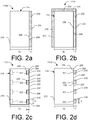
- Figures 2a-2h show side views of examples of a scintillator, similar to the scintillator 110, with like numbers referring to like elements.
- the various scintillators shown in Figures 2a-2h help to show some of various examples of an inorganic scintillator portion 112 and an organic scintillator portion 114.
- the inorganic scintillator portion 112 of a scintillator 110a comprises an inorganic material element 202.
- the inorganic material element 202 comprises an outer surface 204 and an inner surface 206, with the inner surface 206 opposite the outer surface 204.
- the outer surface 204 is configured to be proximate to the subject 120 to be scanned with the x-ray backscattering system 102 such that the outer surface 204 is configured to receive x-ray photons 122 scattered by the subject 120.
- the inorganic material element 202 has a thickness T1, defined between the outer surface 204 and the inner surface 206.
- the thickness T1 may be selected to correspond to energies of x-rays to be emitted by the x-ray backscattering system 102. In some embodiments, the thickness T1 is between 1 and 100 microns. In particular, the thickness T1 may be about 10 microns.
- the organic scintillator portion 114 of the scintillator 110a comprises a front surface 208 and a back surface 210, with the back surface 210 opposite the front surface 208. At least a portion of the front surface 208 abuts the inner surface 206 of the inorganic material element 202.
- the organic scintillator portion 114 has a thickness T2, defined between the front surface 208 and the back surface 210.
- the thickness T2 may be selected to correspond to energies of x-rays 118 to be emitted by the x-ray backscattering system 102. In some embodiments, the thickness T2 is between .5 and 10 inches. In particular, the thickness T1 may be about 1 inch.
- FIG. 2b another example of a scintillator 110b comprises multiple inorganic scintillator portions disposed on multiple surfaces of the organic scintillator portion 114.
- the scintillator 110b may include a second inorganic scintillator portion 212, made of a second inorganic scintillating material, disposed on the back surface 210 of the organic scintillator portion 114. Additionally or alternatively, the scintillator 110b may include a third inorganic scintillator portion 214, made of a third inorganic scintillating material, disposed on one or more side surfaces 216 of the organic scintillator portion 114. The side surfaces 216 may include any or all surfaces extending between the front surface 208 and the back surface 210.
- the first inorganic scintillating material and the second inorganic scintillating material may be the same. Additionally or alternatively, the first and the third inorganic scintillating material may be the same, the second and the third inorganic scintillating material may be the same, or each of the scintillating materials may be the same. In other embodiments, each of the inorganic scintillating materials may be different.
- the inorganic scintillator portion 112 comprises an inorganic material element 202 disposed upon substantially all of the front surface 208 of the organic scintillator portion 114.
- the inorganic scintillator portion 112 comprises a plurality of inorganic material elements 202 and only a portion of the front surface 208 abuts an inner surface 206 the plurality of inorganic material elements 202.
- the inorganic scintillator portion 112 of scintillators 110b-110h comprises a plurality of inorganic material elements 202.
- Each of the inorganic material elements 202 comprise an outer surface 204 configured to be proximate to the subject 120 and an inner surface 206 opposite the outer surface. As shown, each of the inorganic material elements 202 are space apart relative to each other.
- the inorganic material elements 202 have respective diameters (D), which may be common for all or some of the inorganic material elements 202.
- the front surface 208 of the organic scintillator portion 114 comprises one or more spaced-apart first sections 218 and one or more second sections 220, which second sections 220 may be connected or spaced-apart.
- the inorganic material elements 202 are disposed on corresponding spaced-apart first sections 218 of the front surface 208 of the organic scintillator portion 114.
- the second sections 220 of the front surface 208 of the organic scintillator portion 114 are devoid of the inorganic material elements 202.
- the scintillator 110c comprises a plurality of inorganic scintillator elements 202 embedded in the organic scintillator portion 114.
- the one or more spaced-apart first sections 218 of the front surface 208 are recessed from the one or more second sections 220 of the front surface 208.
- a thickness T2 is greater between the back surface and the one or more second sections 220 than a thickness between the back surface and the one or more spaced-apart first sections 218.
- the outer surface 204 of one or more of the inorganic scintillator elements 202 may be generally coplanar with the one or more second sections 220 of the front surface 208.
- an additional set of inorganic scintillator elements 202 are embedded in the back surface 210 of the organic scintillator portion 114, as shown in dashed line.
- the inorganic scintillator elements 202 of the scintillator 110c may be, for example, cylindrical or a rectangular prism.
- the scintillator 110d comprises a plurality of inorganic scintillator elements 202 disposed on a generally planar portion of the front surface 208.
- the one or more spaced-apart first sections 218 of the front surface 208 are generally coplanar with the one or more second sections 220 of the front surface 208 between the one or more spaced-apart first sections.
- the scintillator 110e comprises a plurality of inorganic scintillator elements 202 partially embedded in the organic scintillator portion 114.
- the one or more spaced-apart first sections 218 of the front surface 208 are recessed from the one or more second sections 220 of the front surface 208.
- the outer surface 204 of the inorganic scintillator elements 202 extend outwardly from the one or more second sections 220 (i.e., the one or more second sections 220 are recessed from the outer surface 204).
- the scintillator 110f comprises a plurality of inorganic scintillator elements 202 embedded in the organic scintillator portion 114.
- Each of the inorganic scintillator elements 202 has a diameter D that decreases from the outer surface 204 to the inner surface 206.
- the inorganic scintillator elements 202 have angled side surfaces that are not orthogonal to one or both of the outer surface 204 and the inner surface 206.
- These angled side surfaces may increase a probability that x-ray photons 122 passing through the inorganic scintillator elements 202 hit the organic scintillator portion 114 at surface that is not orthogonal to the path of the x-ray photons 122. This may increase a likelihood that the x-ray photons 122 travel a longer distance through the scintillator 114, and likewise increase a probability of the scintillator 110 absorbing energy from the x-ray photons 122 and producing a detectable photoelectric emission.
- the inorganic scintillator elements 202 of the scintillator 110f may be, for example, frustoconical or a trapezoidal prism.
- the scintillator 110g comprises a plurality of inorganic scintillator elements 202 embedded in the organic scintillator portion 114. Similar to the inorganic scintillator elements 202 of the scintillator 110f, each of the inorganic scintillator elements 202 of the scintillator 110g has a diameter D that decreases from the outer surface 204 to the inner surface 206. However, in contrast, the inner surface 206 of the scintillator 110g is an edge or a point, rather than a surface that is generally parallel to the outer surface 204.
- the inorganic scintillator elements 202 of the scintillator 110g may be, for example, conical or a triangular prism.
- the scintillator 110h comprises a plurality of inorganic scintillator elements 202 partially embedded in the organic scintillator portion 114. Similar to the inorganic scintillator elements 202 of the scintillator 110f, each of the inorganic scintillator elements 202 of the scintillator 110g has a diameter D that decreases from the outer surface 204 to the inner surface 206. However, in contrast, the inorganic scintillator elements 202 include a portion with a generally uniform diameter.
- the portion with the generally uniform diameter may be the portion of the inorganic scintillator elements 202 that is not embedded in the organic scintillator portion 114 (i.e., the portion outward from the second sections 220 of the front surface 208 of the organic scintillator portion 114).
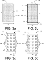
- FIGS 3a-3d show top views of non-limiting examples of various scintillators 110i through 110l, which can be scintillators of the x-ray backscattering system 102. Aspects of one or more of the scintillators 110i-110l may be combined with aspects of one or more of the scintillators 110a-110h.
- the scintillator 110i comprises an inorganic material element 202, having an outer surface 204, disposed upon substantially all of the front surface 208 of the organic scintillator portion 114 (shown in Figures 2a-2h ).
- the outer surface 204 of the inorganic material element 202 has a diameter D and a width W1.
- the scintillator 110j comprises an inorganic material element 202, having an outer surface 204, disposed upon substantially all of the front surface 208 of the organic scintillator portion 114 (shown in Figures 2a-2h ).
- the outer surface 204 of the inorganic material element 202 has a diameter D and a width W1.
- the scintillator 110j includes a third inorganic scintillator portion 214, made of a third inorganic scintillating material, disposed on one or more side surfaces 216 of the organic scintillator portion 114.
- the side surfaces 216 may include any or all surfaces extending between the front surface 208 and the back surface 210.
- the scintillator 110k comprises a plurality of inorganic material elements 202, having outer surfaces 204, disposed upon spaced-apart first sections 218 (shown in Figures 2a-2h ) of the front surface 208 of the organic scintillator portion 114.
- a second section 220 of the front surface 208 is devoid of the inorganic material elements 202.
- the inorganic material elements 202 have a diameter D and a width W1, which may be the same for all inorganic material elements 202. Alternatively, one or more of the diameter D and the width W1 may be different for respective ones or groups of inorganic material elements 202.
- the organic scintillator portion 114 has a width W2 that may be greater than the width W1 of the inorganic material elements 202.
- the inorganic material elements 202 of the scintillator 110k may be, for example, cylindrical or conical. Additionally or alternatively, the inorganic material elements 202 may be embedded or partially embedded into the organic scintillator portion 114.
- the inorganic material elements 202 may be distributed evenly, randomly, or with different predetermined densities across the front surface 208 of the organic scintillator portion 114.
- the inorganic material elements 202 may be distributed with relatively high density at a location of the scintillator 110k that is closest to the x-ray source and with a relatively low density at a location of the scintillator 110 that is farthest from the x-ray source.
- the scintillator 110l comprises a plurality of inorganic material elements 202, having outer surfaces 204, disposed upon spaced-apart first sections 218 (shown in Figures 2a-2h ) of the front surface 208 of the organic scintillator portion 114.
- a second section 220 of the front surface 208 is devoid of the inorganic material elements 202.
- the inorganic material elements 202 of the scintillator 110l have a diameter D and a width W1, which may be the same for all inorganic material elements 202. Alternatively, one or more of the diameter D and the width W1 may be different for respective ones or groups of inorganic material elements 202.
- the organic scintillator portion 114 has a width W2 that may be greater than the width W1 of the inorganic material elements 202.
- the inorganic material elements 202 of the scintillator 110k may be, for example, a rectangular or trapezoidal prism. Additionally or alternatively, the inorganic material elements 202 may be embedded or partially embedded into the organic scintillator portion 114. Further, the inorganic material elements 202 may be distributed evenly, randomly, or with different predetermined densities across the front surface 208 of the organic scintillator portion 114.
- the process 400 may be used to produce any one or more of the examples of the scintillator 110 disclosed herein.
- the process 400 optionally includes disposing a layer 402 of organic scintillating material on a substrate 404.
- the layer 402 has a thickness (T2), defined between a front surface 406 and a back surface 408, that is generally uniform.
- T2 of the layer 402 of organic scintillating material is between .5 and 10 inches. In particular, the thickness T2 may be about 1 inch.
- the process 400 then includes forming a plurality of voids 410 within the front surface 406 of the layer 402 of the organic scintillating material.
- some of the organic scintillating material may be removed (e.g., via etching) from a plurality of sections of the front surface 406 of the layer 402.
- additional organic scintillating material may be disposed at a plurality of sections of the front surface 406 of the layer 402 such that voids are created in remaining sections of the front surface 406 of the layer 402.
- the voids 410 have a thickness T3, which is less than the thickness T2 of the layer 402 of organic scintillating material.
- each of the voids 410 have substantially the same thickness T3, while in other embodiments, the voids have different thicknesses T3.
- the voids 410 may have a thickness between 1 and 100 microns. More particularly, the voids 410 may have a thickness of about 10 microns.
- the process 400 includes disposing one or more inorganic material elements 412, having a thickness T1, within one or more of the plurality of voids 412.
- this step includes disposing a layer of inorganic scintillating material upon the entire front surface 406 of the layer 402 of organic scintillating material and then removing a portion of the inorganic scintillating material to leave spaced-apart inorganic material elements 412 embedded in the layer 402 of organic scintillating material.
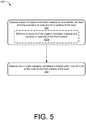
- FIG. 5 shows a method 500, according to certain examples, for producing the scintillator 110.
- the method 500 is performed in producing any one or more of the examples of the scintillator 110 disclosed herein.
- the method 500 includes (block 502) disposing a layer 402 of organic scintillating material on a substrate 404, the layer 402 defining a plurality of voids 410 at a front surface 406 of the layer 402.
- the layer 402 of organic scintillating material comprises a back surface 210, 408 adjacent to the substrate 404, and a front surface 208, 406.
- This operation (block 502) optionally includes (block 502a) removing an amount of the organic scintillating material at a plurality of locations of the front surface 208, 406 to provide the plurality of voids 410.
- the method 500 further includes (block 504) disposing one or more inorganic scintillator elements 202, 412 within one or more of the plurality of voids 410.
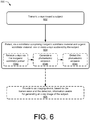
- Figure 6 shows a method 600, according to certain examples, of operation of an x-ray backscattering system 102.
- the method 600 is performed using any one or more of the examples of the scintillator 110 disclosed herein.
- the method 600 includes (block 602) transmitting x-rays 118 toward a subject 120.
- the method may include transmitting, via an x-ray tube 104 of the x-ray backscattering system 102, x-rays 118 toward a subject 120.
- the method also includes (block 604) detecting, via a scintillator 110 of the x-ray backscattering system 102, one or more x-ray photons 122 scattered by the subject 120.
- the scintillator 110 may be any one of the scintillators 110 disclosed herein.
- the scintillator 110 comprises an inorganic scintillator portion 112 made of an inorganic scintillating material and comprising one or more inorganic material elements 202.
- Each inorganic material element 202 of the one or more inorganic material elements 202 comprises an outer surface 204 proximate to the subject 120 and an inner surface 206 opposite the outer surface 204.
- the scintillator 110 also comprises an organic scintillator portion 114 made of an organic scintillating material and comprising a front surface 208. At least a portion of the front surface 208 abuts the inner surface 206 of at least one of the one or more inorganic material elements 202.
- the (block 604) detecting may optionally include (block 604a) receiving at least one of the one or more x-ray photons 122 via the inorganic scintillator portion 112.
- the (block 604) detecting may also include generating 604b, in response to (block 604) receiving the at least one of the one or more x-ray photons 122, a photoelectric emission within the scintillator 110.
- the (block 604) detecting may further include (604c) detecting the photoelectric emission via a photomultiplier tube 116 of the x-ray backscattering system 102.
- the method optionally includes (block 606) providing to an imaging device 124, based on (block 602) transmitting and (block 604) detecting, information usable for generating an x-ray image (126) of the subject 120.
- instances in this specification where one element is "coupled" to another element can include direct and indirect coupling.
- Direct coupling can be defined as one element coupled to and in some contact with another element.
- Indirect coupling can be defined as coupling between two elements not in direct contact with each other, but having one or more additional elements between the coupled elements.
- securing one element to another element can include direct securing and indirect securing.
- adjacent does not necessarily denote contact. For example, one element can be adjacent another element without being in contact with that element.
- the phrase "at least one of', when used with a list of items, means different combinations of one or more of the listed items may be used and only one of the items in the list may be needed.
- the item may be a particular object, thing, or category.
- "at least one of' means any combination of items or number of items may be used from the list, but not all of the items in the list may be required.
- "at least one of item A, item B, and item C" may mean item A; item A and item B; item B; item A, item B, and item C; or item B and item C.
- "at least one of item A, item B, and item C” may mean, for example, without limitation, two of item A, one of item B, and ten of item C; four of item B and seven of item C; or some other suitable combination.
- first, second, etc. are used herein merely as labels, and are not intended to impose ordinal, positional, or hierarchical requirements on the items to which these terms refer. Moreover, reference to, e.g., a “second” item does not require or preclude the existence of, e.g., a "first” or lower-numbered item, and/or, e.g., a "third" or higher-numbered item.
- a system, apparatus, structure, article, element, component, or hardware “configured to” perform a specified function is indeed capable of performing the specified function without any alteration, rather than merely having potential to perform the specified function after further modification.
- the system, apparatus, structure, article, element, component, or hardware “configured to” perform a specified function is specifically selected, created, implemented, utilized, programmed, and/or designed for the purpose of performing the specified function.
- "configured to” denotes existing characteristics of a system, apparatus, structure, article, element, component, or hardware which enable the system, apparatus, structure, article, element, component, or hardware to perform the specified function without further modification.
- a system, apparatus, structure, article, element, component, or hardware described as being “configured to” perform a particular function may additionally or alternatively be described as being “adapted to” and/or as being “operative to” perform that function.
- the schematic flow chart diagrams included herein are generally set forth as logical flow chart diagrams. As such, the depicted order and labeled steps are indicative of one example of the presented method. Other steps and methods may be conceived that are equivalent in function, logic, or effect to one or more steps, or portions thereof, of the illustrated method. Additionally, the format and symbols employed are provided to explain the logical steps of the method and are understood not to limit the scope of the method. Although various arrow types and line types may be employed in the flow chart diagrams, they are understood not to limit the scope of the corresponding method. Indeed, some arrows or other connectors may be used to indicate only the logical flow of the method. For instance, an arrow may indicate a waiting or monitoring period of unspecified duration between enumerated steps of the depicted method. Additionally, the order in which a particular method occurs may or may not strictly adhere to the order of the corresponding steps shown.
Landscapes
- Chemical & Material Sciences (AREA)
- Physics & Mathematics (AREA)
- Life Sciences & Earth Sciences (AREA)
- General Physics & Mathematics (AREA)
- Organic Chemistry (AREA)
- Materials Engineering (AREA)
- Engineering & Computer Science (AREA)
- Health & Medical Sciences (AREA)
- Inorganic Chemistry (AREA)
- High Energy & Nuclear Physics (AREA)
- Analytical Chemistry (AREA)
- Pathology (AREA)
- Immunology (AREA)
- General Health & Medical Sciences (AREA)
- Biochemistry (AREA)
- Crystallography & Structural Chemistry (AREA)
- Molecular Biology (AREA)
- Spectroscopy & Molecular Physics (AREA)
- General Life Sciences & Earth Sciences (AREA)
- Geophysics (AREA)
- Measurement Of Radiation (AREA)
- Analysing Materials By The Use Of Radiation (AREA)
Abstract
Description
- This disclosure relates generally to detection of scattered x-rays in x-ray backscattering systems, and more particularly detection of scattered x-rays using a scintillator comprising inorganic scintillating material and organic scintillating material.
- An x-ray backscattering system can be used to non-destructively inspect a subject, including detecting non-line-of-site features of the subject. Conventional x-ray backscattering systems include an x-ray tube and detectors. The detectors include a photomultiplier tube (PMT) and scintillators. The x-ray tube emits x-rays toward the subject. When the x-rays collide with components of the subject, the x-rays diffract and some of the x-ray photons travel toward the detectors. When the x-ray photons hit an outer surface of a scintillator, some x-rays reflect off of the outer surface and some x-rays penetrate the outer surface. Of the x-rays that penetrate the outer surface, some x-rays hit a back surface of the scintillator and reflect back within the scintillator, while others penetrate the back surface and exit the scintillator.
- The PMT detects photoelectric emissions that occur when an electron of an atom of the scintillator absorbs energy from an x-ray to excite the electron to a higher-energy state, which electron then falls back to its initial state while causing the photoelectric emission. The PMT may detect a quantity of photoelectric emissions within the scintillator. Alternatively, the PMT may detect a brightness of the total effect of the photoelectric emissions within the scintillator.
- Some deficiencies with conventional x-ray backscattering systems involve an inability to absorb energy from x-rays traveling toward the detectors. For example, when x-rays reflect off of the outer surface of the scintillator or penetrate the back surface and exit the scintillator, opportunities to absorb energy from the x-rays are lost. These deficiencies may be caused by a large distribution of energies of various x-rays diffracted from the components of the subject. For example, a scintillator calibrated (e.g., by a selected thickness of material) for x-rays having a median expected energy may result in relatively low energy x-rays reflecting off of the outer surface and/or relatively high energy x-rays penetrating through the back surface.
- To compensate for some of these deficiencies, some x-ray backscattering systems use a relatively high x-ray power supply to generate a sufficient quantity of x-rays for which the scintillator is calibrated. This way, even though the scintillator may not absorb energy from low energy and high energy x-rays, the scintillator can still detect enough x-rays to provide information for imaging the subject. However, these high-power x-ray backscattering systems are more expensive to produce and operate and less portable.
- Therefore, a need exists for an x-ray backscattering system that has a scintillator configured to absorb energy from x-rays having a relatively broad range of energies.
- The subject matter of the present application provides example scintillators, x-ray backscattering systems implementing such scintillators, methods of using scintillators, and methods of manufacturing scintillators that overcome the above-discussed shortcomings of prior art techniques. The subject matter of the present application has been developed in response to the present state of the art, and in particular, in response to shortcomings of conventional scintillators, and the conventional methods and systems for producing scintillators and operating x-ray backscattering systems to detect x-rays.
- Disclosed herein is a scintillator comprising an inorganic scintillator portion made of an inorganic scintillating material and comprising an organic scintillator portion made of an organic scintillator portion made of an organic scintillating material. The inorganic scintillator portion comprises one or more inorganic material elements. Each of the inorganic material elements comprises an outer surface and an inner surface, opposite the outer surface. The outer surface is configured to be proximate to a subject to be scanned with the x-ray backscattering system, such that the outer surface is configured to receive x-ray photons scattered by the subject. The organic scintillator portion comprises a front surface, wherein at least a portion of the front surface abuts the inner surface of at least one of the one or more inorganic material elements. The preceding subject matter of this paragraph characterizes example 1 of the present disclosure.
- The inorganic scintillator portion further comprises a plurality of the inorganic material elements, spaced apart relative to each other. The plurality of the inorganic material elements are disposed on corresponding spaced-apart first sections of the front surface of the organic scintillator portion. The second sections of the front surface of the organic scintillator portion are devoid of the inorganic material elements. The preceding subject matter of this paragraph characterizes example 2 of the present disclosure, wherein example 2 also includes the subject matter according to example 1, above.
- The plurality of spaced-apart first sections of the front surface of the organic scintillator portion are recessed from the second sections of the front surface of the organic scintillator portion that is devoid of the inorganic scintillating material. The preceding subject matter of this paragraph characterizes example 3 of the present disclosure, wherein example 3 also includes the subject matter according to example 2, above.
- The inorganic scintillator portion comprises an inorganic material element disposed upon substantially all of the front surface of the organic scintillator portion. The preceding subject matter of this paragraph characterizes example 4 of the present disclosure, wherein example 4 also includes the subject matter according example 1, above.
- The inorganic scintillating material has an index of refraction that is different from an index of refraction of the organic scintillating material. The preceding subject matter of this paragraph characterizes example 5 of the present disclosure, wherein example 5 also includes the subject matter according to any one of examples 1-4, above.
- The scintillator further comprises a second inorganic scintillator portion made of a second inorganic scintillating material. The organic scintillator portion further comprises a back surface, opposite the front surface. The second inorganic scintillator portion is disposed on the back surface of the organic scintillator portion. The preceding subject matter of this paragraph characterizes example 6 of the present disclosure, wherein example 6 also includes the subject matter according to any one of examples 1-5, above.
- The inorganic scintillating material and the second inorganic scintillating material are the same. The preceding subject matter of this paragraph characterizes example 7 of the present disclosure, wherein example 7 also includes the subject matter according to example 6, above.
- The scintillator comprises a third inorganic scintillator portion made of a third inorganic scintillating material. The organic scintillator portion further comprises one or more side surfaces that extend between the front surface and the back surface. The third inorganic scintillator portion is disposed on the one or more side surfaces of the organic scintillator portion. The preceding subject matter of this paragraph characterizes example 8 of the present disclosure, wherein example 8 also includes the subject matter according to any one of examples 6-7, above.
- The organic scintillating material comprises one or more of plastic and polyurethane. The preceding subject matter of this paragraph characterizes example 9 of the present disclosure, wherein example 9 also includes the subject matter according to any one of examples 1-8, above.
- The inorganic scintillating material comprises one or more of lead iodide (PbI2), calcium tungstate (CaWO4), and cesium iodide (CsI). The preceding subject matter of this paragraph characterizes example 10 of the present disclosure, wherein example 10 also includes the subject matter according to any one of examples 1-9, above.
- Each of the one or more inorganic material elements have a thickness, defined between the outer surface and the inner surface. The thickness corresponds to an energy of x-rays to be emitted by the x-ray backscattering system. The preceding subject matter of this paragraph characterizes example 11 of the present disclosure, wherein example 11 also includes the subject matter according to any one of examples 1-10, above.
- The organic scintillator portion further comprises a back surface, opposite the front surface. The organic scintillator portion is configured with a thickness, defined between the front surface and the back surface. The thickness corresponds to an energy of x-rays to be used in the x-ray backscattering system. The preceding subject matter of this paragraph characterizes example 12 of the present disclosure, wherein example 12 also includes the subject matter according to any one of examples 1-11, above.
- The organic scintillator portion couples the
inorganic scintillator portion 112 with a photomultiplier tube. The preceding subject matter of this paragraph characterizes example 13 of the present disclosure, wherein example 13 also includes the subject matter according to any one of examples 1-12, above. - Additionally disclosed herein is a method of producing a scintillator. The method comprises disposing a layer of organic scintillating material on a substrate. The layer of organic scintillating material comprises a back surface, adjacent to the substrate, and a front surface. The layer of organic scintillating material defines a plurality of voids at the front surface. The method also comprises disposing one or more inorganic material elements within one or more of the plurality of voids. The preceding subject matter of this paragraph characterizes example 14 of the present disclosure.
- Disposing a layer of organic scintillating material on a substrate comprises removing an amount of the organic scintillating material at a plurality of locations of the front surface. The removed amount of organic scintillating material defining the plurality of voids at the front surface. The preceding subject matter of this paragraph characterizes example 15 of the present disclosure, wherein example 15 also includes the subject matter according to example 14, above.
- The plurality of voids have thicknesses between 1 and 100 microns. The preceding subject matter of this paragraph characterizes example 16 of the present disclosure, wherein example 16 also includes the subject matter according to any of examples 14 and 15, above.
- The layer of organic scintillating material has a thickness, defined between the front surface and the back surface. The thickness of the layer of organic scintillating material is between .5 and 10 inches. The preceding subject matter of this paragraph characterizes example 17 of the present disclosure, wherein example 17 also includes the subject matter according to any of examples 14-16, above.
- Further disclosed herein is a method of operation of an x-ray backscattering system. The method comprises transmitting, via an x-ray tube of the x-ray backscattering system, x-rays toward a subject. The method also comprises detecting, via a scintillator of the x-ray backscattering system, one or more x-ray photons scattered by the subject. The scintillator comprises an inorganic scintillator portion, made of an inorganic scintillating material, and an organic scintillator portion made of an organic scintillating material. The inorganic scintillating material comprises one or more inorganic material elements. Each inorganic material element of the one or more inorganic material elements comprises an outer surface proximate to the subject and an inner surface opposite the outer surface. The organic scintillator portion comprises a front surface, wherein at least a portion of the front surface abuts the inner surface of at least one of the one or more inorganic material elements. The preceding subject matter of this paragraph characterizes example 18 of the present disclosure.
- Detecting one or more x-ray photons scattered by the subject comprises receiving at least one of the one or more x-ray photons via the inorganic scintillator portion. Detecting one or more x-ray photons scattered by the subject also comprises generating, in response receiving the at least one of the one or more x-ray photons, a photoelectric emission within the scintillator. Detecting one or more x-ray photons scattered by the subject further comprises detecting the photoelectric emission via a photomultiplier tube of the x-ray backscattering system. The preceding subject matter of this paragraph characterizes example 19 of the present disclosure, wherein example 19 also includes the subject matter according to example 18, above.
- The method further comprises providing to an imaging device, based on transmitting and detecting, information usable for generating an x-ray image of the subject. The preceding subject matter of this paragraph characterizes example 20 of the present disclosure, wherein example 20 also includes the subject matter according to any one of examples 18-19, above.
- The described features, structures, advantages, and/or characteristics of the subject matter of the present disclosure may be combined in any suitable manner in one or more examples, including embodiments and/or implementations. In the following description, numerous specific details are provided to impart a thorough understanding of examples of the subject matter of the present disclosure. One skilled in the relevant art will recognize that the subject matter of the present disclosure may be practiced without one or more of the specific features, details, components, materials, and/or methods of a particular example, embodiment, or implementation. In other instances, additional features and advantages may be recognized in certain examples, embodiments, and/or implementations that may not be present in all examples, embodiments, or implementations. Further, in some instances, well-known structures, materials, or operations are not shown or described in detail to avoid obscuring aspects of the subject matter of the present disclosure. The features and advantages of the subject matter of the present disclosure will become more fully apparent from the following description and appended claims, or may be learned by the practice of the subject matter as set forth hereinafter.
- In order that the advantages of the subject matter may be more readily understood, a more particular description of the subject matter briefly described above will be rendered by reference to specific examples that are illustrated in the appended drawings. Understanding that these drawings depict only typical examples of the subject matter, they are not therefore to be considered to be limiting of its scope. The subject matter will be described and explained with additional specificity and detail through the use of the drawings, in which:
-
Figure 1 is a schematic perspective view of an x-ray backscattering system, inspecting a part, according to one or more examples of the present disclosure; -
Figures 2a-2h are side views of respective examples of a scintillator of the x-ray backscattering system ofFigure 1 ; -
Figures 3a-3d are top views of respective examples of a scintillator of the x-ray backscattering system ofFigure 1 ; -
Figure 4 is a schematic flow diagram of a process of manufacturing a scintillator, from a side view of the scintillator, according to one or more examples of the present disclosure; -
Figure 5 is a flow diagram of a method of manufacturing a scintillator, according to one or more examples of the present disclosure; and -
Figure 6 is a flow diagram of a method of operation of an x-ray backscattering system, according to one or more examples of the present disclosure. - Reference throughout this specification to "one example," "an example," or similar language means that a particular feature, structure, or characteristic described in connection with the example is included in at least one example of the present disclosure. Appearances of the phrases "in one example," "in an example," and similar language throughout this specification may, but do not necessarily, all refer to the same example. Similarly, the use of the term "implementation" means an implementation having a particular feature, structure, or characteristic described in connection with one or more examples of the present disclosure, however, absent an express correlation to indicate otherwise, an implementation may be associated with one or more examples.
- Disclosed herein are scintillators that each have an organic scintillator portion and an inorganic scintillator portion. The inorganic scintillator portion includes inorganic scintillating material disposed upon all, or a portion of, of a front surface of the organic scintillator portion. Further, in some examples, the inorganic scintillator portion is also disposed on a back surface and/or side surfaces of the organic scintillator portion.
- The inorganic scintillating material may be embedded into the front surface of the organic scintillating material. For example, a process of manufacturing a scintillator may include disposing a layer of organic scintillating material on a substrate, with the layer of organic scintillating material defining a plurality of voids at its front surface. The process then includes disposing one or more inorganic material elements within the plurality of voids, thus embedding the inorganic material elements into the front surface of the layer of organic scintillating material.
- When compared with a conventional x-ray backscattering system operating with a same power supply, an x-ray backscattering system having one or more scintillators, as described herein, may detect an increased quantity of photoelectric emissions based on absorbing additional energy from scattered x-rays having relatively high and/or relatively low energies. This can be used to produce an x-ray image with improved resolution. Additionally, when compared with conventional x-ray backscattering systems that produce an x-ray image with similar resolution, the x-ray backscattering system described herein may consume less power, have lower manufacturing costs, and/or have better portability based on size and weight of the system.
- Referring to
Figure 1 , according to some examples, disclosed herein is anon-destructive inspection system 100 in which anx-ray backscattering system 102 can be implemented according to one or more examples of the present disclosure. Thex-ray backscattering system 102 includes an x-ray source, such as anx-ray tube 104. Thex-ray tube 104 may include anx-ray emitter 106 and anaperture 108 through which emitted x-rays can exit thex-ray tube 104 toward a subject for scanning. - The
x-ray backscattering system 102 also includes one ormore scintillators 110. The one ormore scintillators 110 include aninorganic scintillator portion 112 made of an inorganic scintillating material, such as one or more of lead iodide (PbI2), calcium tungstate (CaWO4), and cesium iodide (CsI). The one ormore scintillators 110 also include anorganic scintillator portion 114 made of an organic scintillating material, such as a plastic, polyurethane, or another carbon-based material. - In some embodiments, the inorganic scintillating material has an index of refraction that is different from an index of refraction of the organic scintillating material. This may cause
x-ray photons 122, upon hitting an interface between theinorganic scintillator portion 112 and theorganic scintillator portion 114, to change their vectors. For example, one or more of thex-ray photons 122 may reflect back within theinorganic scintillator portion 112. Additionally or alternatively, one or more of thex-ray photons 122 may penetrate theorganic scintillator portion 114 and may change its trajectory upon penetration. A change of vector may cause thescintillator 110 to absorb energy from thex-ray photons 122 and cause photoelectric emissions for detection by thePMT 116, as described below. - The
x-ray backscattering system 102 also includes a photomultiplier tube (PMT) 116 coupled to thescintillator 110. For example, thePMT 116 may be coupled to theorganic scintillator portion 114, which couples theinorganic scintillator portion 112 with thePMT 116. Collectively, thescintillator 110 and thePMT 116 may be defined as a detector. - In an example operation of the
x-ray backscattering system 102, thex-ray emitter 106 draws from a power supply to emitx-rays 118 via theaperture 108 toward a subject 120. The subject 120 is a part (e.g., component, device, assembly, etc.) prior to use or after use. Moreover, the subject 120 can be removed from a larger assembly for inspection or it may be inspected while in situ on or in the larger assembly. When thex-rays 118 collide with components of the subject 120, thex-rays 118 diffract, resulting in some of the diffractedx-ray photons 122 traveling toward the one ormore scintillators 110. - When the diffracted
x-ray photons 122 hit an outer surface of thescintillator 110, at least some of the diffractedx-ray photons 122 enter theinorganic scintillator portion 112 before hitting theorganic scintillator portion 114. A set of the diffractedx-ray photons 122 that enter the inorganicscintillating material 112 transfer energy to particles of one or both of theorganic scintillator portion 114 and theinorganic scintillator portion 112, which in turn release photoelectric emissions that are detected by thePMT 116. This process can be described as thescintillator 110 absorbing energy from the diffractedx-ray photons 122. Because thescintillator 110 includes theinorganic scintillator portion 112 and theorganic scintillator portion 114, thescintillator 110 is more likely to absorb energy from diffractedx-ray photons 122 having relatively high and/or relatively low energies. - The
PMT 116 may then provide information, based on the detection of photoelectric emissions, to animaging device 124 of thenon-destructive inspection system 100. Theimaging device 124 is usable for generating anx-ray image 126 of the subject 120. The information may include a count of detected photoelectric emissions or an indication of a brightness based on detection of photoelectric emissions. The count or brightness may also be associated with a location of the subject 120. For example, the count or brightness may be associated with a location of the subject 120 at which thex-rays 118 are directed. The information may further include a plurality of counts or brightnesses, each associated with a respective one of a plurality of locations of the subject 120 at which thex-rays 118 are directed. This association may be determined based on a time at which thePMT 116 detects photoelectric emissions and an indication of a location of the subject 120 at which thex-rays 118 are directed at the time of detection. -
Figures 2a-2h show side views of examples of a scintillator, similar to thescintillator 110, with like numbers referring to like elements. The various scintillators shown inFigures 2a-2h help to show some of various examples of aninorganic scintillator portion 112 and anorganic scintillator portion 114. - Referring to
Figure 2a , according to one example, theinorganic scintillator portion 112 of ascintillator 110a comprises aninorganic material element 202. Theinorganic material element 202 comprises anouter surface 204 and aninner surface 206, with theinner surface 206 opposite theouter surface 204. Theouter surface 204 is configured to be proximate to the subject 120 to be scanned with thex-ray backscattering system 102 such that theouter surface 204 is configured to receivex-ray photons 122 scattered by the subject 120. Theinorganic material element 202 has a thickness T1, defined between theouter surface 204 and theinner surface 206. The thickness T1 may be selected to correspond to energies of x-rays to be emitted by thex-ray backscattering system 102. In some embodiments, the thickness T1 is between 1 and 100 microns. In particular, the thickness T1 may be about 10 microns. - The
organic scintillator portion 114 of thescintillator 110a comprises afront surface 208 and aback surface 210, with theback surface 210 opposite thefront surface 208. At least a portion of thefront surface 208 abuts theinner surface 206 of theinorganic material element 202. Theorganic scintillator portion 114 has a thickness T2, defined between thefront surface 208 and theback surface 210. The thickness T2 may be selected to correspond to energies ofx-rays 118 to be emitted by thex-ray backscattering system 102. In some embodiments, the thickness T2 is between .5 and 10 inches. In particular, the thickness T1 may be about 1 inch. - Referring to
Figure 2b , another example of ascintillator 110b comprises multiple inorganic scintillator portions disposed on multiple surfaces of theorganic scintillator portion 114. - In addition to the
inorganic scintillator portion 202 disposed on thefront surface 208 of theorganic scintillator portion 114, thescintillator 110b may include a secondinorganic scintillator portion 212, made of a second inorganic scintillating material, disposed on theback surface 210 of theorganic scintillator portion 114. Additionally or alternatively, thescintillator 110b may include a thirdinorganic scintillator portion 214, made of a third inorganic scintillating material, disposed on one or more side surfaces 216 of theorganic scintillator portion 114. The side surfaces 216 may include any or all surfaces extending between thefront surface 208 and theback surface 210. - The first inorganic scintillating material and the second inorganic scintillating material may be the same. Additionally or alternatively, the first and the third inorganic scintillating material may be the same, the second and the third inorganic scintillating material may be the same, or each of the scintillating materials may be the same. In other embodiments, each of the inorganic scintillating materials may be different.
- In first example of the
scintillator 110a and the second example of thescintillator 110b, shown inFigures 2a and 2b , theinorganic scintillator portion 112 comprises aninorganic material element 202 disposed upon substantially all of thefront surface 208 of theorganic scintillator portion 114. However, in the embodiments discussed below, theinorganic scintillator portion 112 comprises a plurality of inorganicmaterial elements 202 and only a portion of thefront surface 208 abuts aninner surface 206 the plurality of inorganicmaterial elements 202. - Referring to
Figures 2c-2h , theinorganic scintillator portion 112 ofscintillators 110b-110h comprises a plurality of inorganicmaterial elements 202. Each of theinorganic material elements 202 comprise anouter surface 204 configured to be proximate to the subject 120 and aninner surface 206 opposite the outer surface. As shown, each of theinorganic material elements 202 are space apart relative to each other. Theinorganic material elements 202 have respective diameters (D), which may be common for all or some of theinorganic material elements 202. - The
front surface 208 of theorganic scintillator portion 114 comprises one or more spaced-apartfirst sections 218 and one or moresecond sections 220, whichsecond sections 220 may be connected or spaced-apart. Theinorganic material elements 202 are disposed on corresponding spaced-apartfirst sections 218 of thefront surface 208 of theorganic scintillator portion 114. Thesecond sections 220 of thefront surface 208 of theorganic scintillator portion 114 are devoid of theinorganic material elements 202. - Referring to
Figure 2c , according to another example, thescintillator 110c comprises a plurality ofinorganic scintillator elements 202 embedded in theorganic scintillator portion 114. The one or more spaced-apartfirst sections 218 of thefront surface 208 are recessed from the one or moresecond sections 220 of thefront surface 208. In other words, a thickness T2 is greater between the back surface and the one or moresecond sections 220 than a thickness between the back surface and the one or more spaced-apartfirst sections 218. Additionally, theouter surface 204 of one or more of theinorganic scintillator elements 202 may be generally coplanar with the one or moresecond sections 220 of thefront surface 208. In some alternative examples, an additional set ofinorganic scintillator elements 202 are embedded in theback surface 210 of theorganic scintillator portion 114, as shown in dashed line. - The
inorganic scintillator elements 202 of thescintillator 110c may be, for example, cylindrical or a rectangular prism. - Referring to
Figure 2d , according to another example, thescintillator 110d comprises a plurality ofinorganic scintillator elements 202 disposed on a generally planar portion of thefront surface 208. The one or more spaced-apartfirst sections 218 of thefront surface 208 are generally coplanar with the one or moresecond sections 220 of thefront surface 208 between the one or more spaced-apart first sections. - Referring to
Figure 2e , according to yet another example, thescintillator 110e comprises a plurality ofinorganic scintillator elements 202 partially embedded in theorganic scintillator portion 114. The one or more spaced-apartfirst sections 218 of thefront surface 208 are recessed from the one or moresecond sections 220 of thefront surface 208. However, in contrast to thescintillator 110c, theouter surface 204 of theinorganic scintillator elements 202 extend outwardly from the one or more second sections 220 (i.e., the one or moresecond sections 220 are recessed from the outer surface 204). - Referring to
Figure 2f , according to a further example, thescintillator 110f comprises a plurality ofinorganic scintillator elements 202 embedded in theorganic scintillator portion 114. Each of theinorganic scintillator elements 202 has a diameter D that decreases from theouter surface 204 to theinner surface 206. In other words, theinorganic scintillator elements 202 have angled side surfaces that are not orthogonal to one or both of theouter surface 204 and theinner surface 206. These angled side surfaces may increase a probability thatx-ray photons 122 passing through theinorganic scintillator elements 202 hit theorganic scintillator portion 114 at surface that is not orthogonal to the path of thex-ray photons 122. This may increase a likelihood that thex-ray photons 122 travel a longer distance through thescintillator 114, and likewise increase a probability of thescintillator 110 absorbing energy from thex-ray photons 122 and producing a detectable photoelectric emission. - The
inorganic scintillator elements 202 of thescintillator 110f may be, for example, frustoconical or a trapezoidal prism. - Referring to
Figure 2g , in another example, thescintillator 110g comprises a plurality ofinorganic scintillator elements 202 embedded in theorganic scintillator portion 114. Similar to theinorganic scintillator elements 202 of thescintillator 110f, each of theinorganic scintillator elements 202 of thescintillator 110g has a diameter D that decreases from theouter surface 204 to theinner surface 206. However, in contrast, theinner surface 206 of thescintillator 110g is an edge or a point, rather than a surface that is generally parallel to theouter surface 204. - The
inorganic scintillator elements 202 of thescintillator 110g may be, for example, conical or a triangular prism. - Referring to
Figure 2h , according to another example, thescintillator 110h comprises a plurality ofinorganic scintillator elements 202 partially embedded in theorganic scintillator portion 114. Similar to theinorganic scintillator elements 202 of thescintillator 110f, each of theinorganic scintillator elements 202 of thescintillator 110g has a diameter D that decreases from theouter surface 204 to theinner surface 206. However, in contrast, theinorganic scintillator elements 202 include a portion with a generally uniform diameter. The portion with the generally uniform diameter may be the portion of theinorganic scintillator elements 202 that is not embedded in the organic scintillator portion 114 (i.e., the portion outward from thesecond sections 220 of thefront surface 208 of the organic scintillator portion 114). -
Figures 3a-3d show top views of non-limiting examples ofvarious scintillators 110i through 110l, which can be scintillators of thex-ray backscattering system 102. Aspects of one or more of thescintillators 110i-110l may be combined with aspects of one or more of thescintillators 110a-110h. - Referring to
Figure 3a , according to another example, thescintillator 110i comprises aninorganic material element 202, having anouter surface 204, disposed upon substantially all of thefront surface 208 of the organic scintillator portion 114 (shown inFigures 2a-2h ). Theouter surface 204 of theinorganic material element 202 has a diameter D and a width W1. - Referring to
Figure 3b , according to another example, thescintillator 110j comprises aninorganic material element 202, having anouter surface 204, disposed upon substantially all of thefront surface 208 of the organic scintillator portion 114 (shown inFigures 2a-2h ). As in thescintillator 110i, theouter surface 204 of theinorganic material element 202 has a diameter D and a width W1. - In addition to the
inorganic scintillator portion 202 disposed on thefront surface 208 of the organic scintillator portion 114 (shown inFigures 2a-2h ), thescintillator 110j includes a thirdinorganic scintillator portion 214, made of a third inorganic scintillating material, disposed on one or more side surfaces 216 of theorganic scintillator portion 114. The side surfaces 216 may include any or all surfaces extending between thefront surface 208 and theback surface 210. - Referring to
Figure 3c , according to another example, thescintillator 110k comprises a plurality of inorganicmaterial elements 202, havingouter surfaces 204, disposed upon spaced-apart first sections 218 (shown inFigures 2a-2h ) of thefront surface 208 of theorganic scintillator portion 114. Asecond section 220 of thefront surface 208 is devoid of theinorganic material elements 202. - The
inorganic material elements 202 have a diameter D and a width W1, which may be the same for all inorganicmaterial elements 202. Alternatively, one or more of the diameter D and the width W1 may be different for respective ones or groups of inorganicmaterial elements 202. Theorganic scintillator portion 114 has a width W2 that may be greater than the width W1 of theinorganic material elements 202. - The
inorganic material elements 202 of thescintillator 110k may be, for example, cylindrical or conical. Additionally or alternatively, theinorganic material elements 202 may be embedded or partially embedded into theorganic scintillator portion 114. - The
inorganic material elements 202 may be distributed evenly, randomly, or with different predetermined densities across thefront surface 208 of theorganic scintillator portion 114. For example, theinorganic material elements 202 may be distributed with relatively high density at a location of thescintillator 110k that is closest to the x-ray source and with a relatively low density at a location of thescintillator 110 that is farthest from the x-ray source. - Referring to
Figure 3d , according to another example, the scintillator 110l comprises a plurality of inorganicmaterial elements 202, havingouter surfaces 204, disposed upon spaced-apart first sections 218 (shown inFigures 2a-2h ) of thefront surface 208 of theorganic scintillator portion 114. Asecond section 220 of thefront surface 208 is devoid of theinorganic material elements 202. - Similar to the
inorganic material elements 202 of thescintillator 110k, theinorganic material elements 202 of the scintillator 110l have a diameter D and a width W1, which may be the same for all inorganicmaterial elements 202. Alternatively, one or more of the diameter D and the width W1 may be different for respective ones or groups of inorganicmaterial elements 202. Theorganic scintillator portion 114 has a width W2 that may be greater than the width W1 of theinorganic material elements 202. - The
inorganic material elements 202 of thescintillator 110k may be, for example, a rectangular or trapezoidal prism. Additionally or alternatively, theinorganic material elements 202 may be embedded or partially embedded into theorganic scintillator portion 114. Further, theinorganic material elements 202 may be distributed evenly, randomly, or with different predetermined densities across thefront surface 208 of theorganic scintillator portion 114. - Now referring to
Figure 4 , according to certain examples, aprocess 400 of producing thescintillator 110 is illustrated. Theprocess 400 may be used to produce any one or more of the examples of thescintillator 110 disclosed herein. Theprocess 400 optionally includes disposing alayer 402 of organic scintillating material on asubstrate 404. Thelayer 402 has a thickness (T2), defined between afront surface 406 and aback surface 408, that is generally uniform. In some implementations, the thickness T2 of thelayer 402 of organic scintillating material is between .5 and 10 inches. In particular, the thickness T2 may be about 1 inch. - The
process 400 then includes forming a plurality ofvoids 410 within thefront surface 406 of thelayer 402 of the organic scintillating material. To form the plurality of voids, some of the organic scintillating material may be removed (e.g., via etching) from a plurality of sections of thefront surface 406 of thelayer 402. Alternatively, additional organic scintillating material may be disposed at a plurality of sections of thefront surface 406 of thelayer 402 such that voids are created in remaining sections of thefront surface 406 of thelayer 402. Thevoids 410 have a thickness T3, which is less than the thickness T2 of thelayer 402 of organic scintillating material. In some implementations, each of thevoids 410 have substantially the same thickness T3, while in other embodiments, the voids have different thicknesses T3. Thevoids 410 may have a thickness between 1 and 100 microns. More particularly, thevoids 410 may have a thickness of about 10 microns. - The
process 400 includes disposing one or moreinorganic material elements 412, having a thickness T1, within one or more of the plurality ofvoids 412. In some implementations, this step includes disposing a layer of inorganic scintillating material upon the entirefront surface 406 of thelayer 402 of organic scintillating material and then removing a portion of the inorganic scintillating material to leave spaced-apartinorganic material elements 412 embedded in thelayer 402 of organic scintillating material. -
Figure 5 shows amethod 500, according to certain examples, for producing thescintillator 110. Themethod 500 is performed in producing any one or more of the examples of thescintillator 110 disclosed herein. Themethod 500 includes (block 502) disposing alayer 402 of organic scintillating material on asubstrate 404, thelayer 402 defining a plurality ofvoids 410 at afront surface 406 of thelayer 402. In some implementations, thelayer 402 of organic scintillating material comprises aback surface substrate 404, and afront surface block 502a) removing an amount of the organic scintillating material at a plurality of locations of thefront surface voids 410. - The
method 500 further includes (block 504) disposing one or moreinorganic scintillator elements voids 410. -
Figure 6 shows a method 600, according to certain examples, of operation of anx-ray backscattering system 102. The method 600 is performed using any one or more of the examples of thescintillator 110 disclosed herein. The method 600 includes (block 602) transmittingx-rays 118 toward a subject 120. For example, the method may include transmitting, via anx-ray tube 104 of thex-ray backscattering system 102,x-rays 118 toward a subject 120. - The method also includes (block 604) detecting, via a
scintillator 110 of thex-ray backscattering system 102, one ormore x-ray photons 122 scattered by the subject 120. Thescintillator 110 may be any one of thescintillators 110 disclosed herein. For example, thescintillator 110 comprises aninorganic scintillator portion 112 made of an inorganic scintillating material and comprising one or moreinorganic material elements 202. Eachinorganic material element 202 of the one or moreinorganic material elements 202 comprises anouter surface 204 proximate to the subject 120 and aninner surface 206 opposite theouter surface 204. Thescintillator 110 also comprises anorganic scintillator portion 114 made of an organic scintillating material and comprising afront surface 208. At least a portion of thefront surface 208 abuts theinner surface 206 of at least one of the one or moreinorganic material elements 202. - The (block 604) detecting may optionally include (
block 604a) receiving at least one of the one ormore x-ray photons 122 via theinorganic scintillator portion 112. The (block 604) detecting may also include generating 604b, in response to (block 604) receiving the at least one of the one ormore x-ray photons 122, a photoelectric emission within thescintillator 110. The (block 604) detecting may further include (604c) detecting the photoelectric emission via aphotomultiplier tube 116 of thex-ray backscattering system 102. - The method optionally includes (block 606) providing to an
imaging device 124, based on (block 602) transmitting and (block 604) detecting, information usable for generating an x-ray image (126) of the subject 120. - In the above description, certain terms may be used such as "up," "down," "upper," "lower," "horizontal," "vertical," "left," "right," "over," "under" and the like. These terms are used, where applicable, to provide some clarity of description when dealing with relative relationships. But, these terms are not intended to imply absolute relationships, positions, and/or orientations. For example, with respect to an object, an "upper" surface can become a "lower" surface simply by turning the object over. Nevertheless, it is still the same object. Further, the terms "including," "comprising," "having," and variations thereof mean "including but not limited to" unless expressly specified otherwise. An enumerated listing of items does not imply that any or all of the items are mutually exclusive and/or mutually inclusive, unless expressly specified otherwise. The terms "a," "an," and "the" also refer to "one or more" unless expressly specified otherwise. Further, the term "plurality" can be defined as "at least two."
- Additionally, instances in this specification where one element is "coupled" to another element can include direct and indirect coupling. Direct coupling can be defined as one element coupled to and in some contact with another element. Indirect coupling can be defined as coupling between two elements not in direct contact with each other, but having one or more additional elements between the coupled elements. Further, as used herein, securing one element to another element can include direct securing and indirect securing. Additionally, as used herein, "adjacent" does not necessarily denote contact. For example, one element can be adjacent another element without being in contact with that element.
- As used herein, the phrase "at least one of', when used with a list of items, means different combinations of one or more of the listed items may be used and only one of the items in the list may be needed. The item may be a particular object, thing, or category. In other words, "at least one of' means any combination of items or number of items may be used from the list, but not all of the items in the list may be required. For example, "at least one of item A, item B, and item C" may mean item A; item A and item B; item B; item A, item B, and item C; or item B and item C. In some cases, "at least one of item A, item B, and item C" may mean, for example, without limitation, two of item A, one of item B, and ten of item C; four of item B and seven of item C; or some other suitable combination.
- Unless otherwise indicated, the terms "first," "second," etc. are used herein merely as labels, and are not intended to impose ordinal, positional, or hierarchical requirements on the items to which these terms refer. Moreover, reference to, e.g., a "second" item does not require or preclude the existence of, e.g., a "first" or lower-numbered item, and/or, e.g., a "third" or higher-numbered item.
- As used herein, a system, apparatus, structure, article, element, component, or hardware "configured to" perform a specified function is indeed capable of performing the specified function without any alteration, rather than merely having potential to perform the specified function after further modification. In other words, the system, apparatus, structure, article, element, component, or hardware "configured to" perform a specified function is specifically selected, created, implemented, utilized, programmed, and/or designed for the purpose of performing the specified function. As used herein, "configured to" denotes existing characteristics of a system, apparatus, structure, article, element, component, or hardware which enable the system, apparatus, structure, article, element, component, or hardware to perform the specified function without further modification. For purposes of this disclosure, a system, apparatus, structure, article, element, component, or hardware described as being "configured to" perform a particular function may additionally or alternatively be described as being "adapted to" and/or as being "operative to" perform that function.
- The schematic flow chart diagrams included herein are generally set forth as logical flow chart diagrams. As such, the depicted order and labeled steps are indicative of one example of the presented method. Other steps and methods may be conceived that are equivalent in function, logic, or effect to one or more steps, or portions thereof, of the illustrated method. Additionally, the format and symbols employed are provided to explain the logical steps of the method and are understood not to limit the scope of the method. Although various arrow types and line types may be employed in the flow chart diagrams, they are understood not to limit the scope of the corresponding method. Indeed, some arrows or other connectors may be used to indicate only the logical flow of the method. For instance, an arrow may indicate a waiting or monitoring period of unspecified duration between enumerated steps of the depicted method. Additionally, the order in which a particular method occurs may or may not strictly adhere to the order of the corresponding steps shown.
- The present subject matter may be embodied in other specific forms without departing from its spirit or essential characteristics. The described examples are to be considered in all respects only as illustrative and not restrictive. All changes which come within the meaning and range of equivalency of the claims are to be embraced within their scope.
- Further, the disclosure comprises embodiments according to the following clauses:
- Clause 1. A scintillator for use in an x-ray backscattering system, the scintillator comprising:
- an inorganic scintillator portion made of an inorganic scintillating material and comprising one or more inorganic material elements, wherein each inorganic material element of the one or more inorganic material elements comprises:
- an outer surface configured to be proximate to a subject to be scanned with the x-ray backscattering system, wherein the outer surface is configured to receive x-ray photons reflected from the subject; and
- an inner surface opposite the outer surface; and
- an organic scintillator portion made of an organic scintillating material and comprising a front surface, wherein at least a portion of the front surface abuts the inner surface of at least one of the one or more inorganic material elements.
- an inorganic scintillator portion made of an inorganic scintillating material and comprising one or more inorganic material elements, wherein each inorganic material element of the one or more inorganic material elements comprises:
- Clause 2. The scintillator according to Clause 1, wherein:
- the inorganic scintillator portion further comprises a plurality of the inorganic material elements, spaced apart relative to each other; and
- the plurality of the inorganic material elements are disposed on corresponding spaced-apart first sections of the front surface of the organic scintillator portion, wherein second sections of the front surface of the organic scintillator portion are devoid of the inorganic material elements.
- Clause 3. The scintillator according to Clause 2, wherein the spaced-apart first sections of the front surface of the organic scintillator portion are recessed from the second sections of the front surface of the organic scintillator portion that is devoid of the inorganic scintillating material.
- Clause 4. The scintillator according to any of Clauses 1-3, wherein the inorganic scintillator portion comprises an inorganic material element disposed upon substantially all of the front surface of the organic scintillator portion.
- Clause 5. The scintillator according to any of Clauses 1-4, wherein the inorganic scintillating material has an index of refraction that is different from an index of refraction of the organic scintillating material.
- Clause 6. The scintillator according to any of Clauses 1-5, further comprising a second inorganic scintillator portion made of a second inorganic scintillating material, wherein:
- the organic scintillator portion further comprises a back surface, opposite the front surface; and
- the second inorganic scintillator portion is disposed on the back surface of the organic scintillator portion.
- Clause 7. The scintillator according to Clause 6, wherein the inorganic scintillating material and the second inorganic scintillating material are the same.
- Clause 8. The scintillator according to any of Clauses 6-7, further comprising a third inorganic scintillator portion made of a third inorganic scintillating material, wherein:
- the organic scintillator portion further comprises one or more side surfaces that extend between the front surface and the back surface; and
- the third inorganic scintillator portion is disposed on the one or more side surfaces of the organic scintillator portion.
- Clause 9. The scintillator according to any of Clauses 1-8, wherein the organic scintillating material comprises one or more of plastic and polyurethane.
- Clause 10. The scintillator according to any of Clauses 1-9, wherein the inorganic scintillating material comprises one or more of lead iodide (PbI2), calcium tungstate (CaWO4), and cesium iodide (CsI).
- Clause 11. The scintillator according to any of Clauses 1-10, wherein:
- each of the one or more inorganic material elements have a thickness (T1), defined between the outer surface and the inner surface; and
- the thickness (T1) corresponds to an energy of x-rays to be emitted by the x-ray backscattering system.
- Clause 12. The scintillator according to any of Clauses 1-11, wherein:
- the organic scintillator portion further comprises a back surface, opposite the front surface;
- the organic scintillator portion is configured with a thickness (T2), defined between the front surface and the back surface; and
- the thickness (T2) corresponds to an energy of x-rays to be used in the x-ray backscattering system.
- Clause 13. The scintillator according to any of Clauses 1-12, wherein the organic scintillating portion couples the inorganic scintillating portion with a photomultiplier tube.
- Clause 14. A method of manufacturing a scintillator, the method comprising:
- disposing a layer of organic scintillating material on a substrate, wherein:
- the layer of organic scintillating material comprises a back surface, adjacent to the substrate, and a front surface; and
- the layer of organic scintillating material defines a plurality of voids at the front surface; and
- disposing one or more inorganic material elements within one or more of the plurality of voids.
- disposing a layer of organic scintillating material on a substrate, wherein:
- Clause 15. The method according to Clause 14, wherein disposing a layer of organic scintillating material on a substrate comprises removing an amount of the organic scintillating material at a plurality of locations of the front surface, the removed amount of organic scintillating material defining the plurality of voids at the front surface.
- Clause 16. The method according to any of Clauses 14-15, wherein plurality of voids have thicknesses (T3) between 1 and 100 microns.
- Clause 17. The method according to any of Clauses 14-16, wherein:
- the layer of organic scintillating material has a thickness (T2), defined between the front surface and the back surface; and
- the thickness (T2) of the layer of organic scintillating material is between 1 and 10 inches.
- Clause 18. A method of operating an x-ray backscattering system, the method comprising:
- transmitting, via an x-ray tube of the x-ray backscattering system, x-rays toward a subject; and
- detecting, via a scintillator of the x-ray backscattering system, one or more x-rays scattered by the subject;
wherein the scintillator comprises:- an inorganic scintillator portion made of an inorganic scintillating material and comprising one or more inorganic material elements, wherein each inorganic material element of the one or more inorganic material elements comprises:
- an outer surface proximate to the subject and an inner surface opposite the outer surface; and
- an organic scintillator portion made of an organic scintillating material and comprising a front surface wherein at least a portion of the front surface abuts the inner surface of at least one of the one or more inorganic material elements.
- Clause 19. The method according to Clause 18, wherein detecting one or more x-rays scattered by the subject comprises:
- receiving at least one of the one or more x-rays via the inorganic scintillator portion;
- generating, in response to receiving the at least one of the one or more x-rays, a photoelectric emission within the scintillator; and
- detecting the photoelectric emission via a photomultiplier tube of the x-ray backscattering system.
- Clause 20. The method according to any of Clauses 18-19, further comprising providing to an imaging device, based on transmitting and detecting, information usable for generating an x-ray image of the subject.
Claims (15)
- A scintillator for use in an x-ray backscattering system (102), the scintillator (110) comprising:an inorganic scintillator portion (112) made of an inorganic scintillating material and comprising one or more inorganic material elements (202), wherein each inorganic material element (202) of the one or more inorganic material elements (202) comprises:an outer surface (204) configured to be proximate to a subject (120) to be scanned with the x-ray backscattering system (102), wherein the outer surface (204) is configured to receive x-ray photons (122) reflected from the subject (120); andan inner surface (206) opposite the outer surface (204); andan organic scintillator portion (114) made of an organic scintillating material and comprising a front surface (208), wherein at least a portion of the front surface (208) abuts the inner surface (206) of at least one of the one or more inorganic material elements (202).
- The scintillator (110) according to claim 1, wherein:the inorganic scintillator portion (112) further comprises a plurality of the inorganic material elements (202), spaced apart relative to each other; andthe plurality of the inorganic material elements (202) are disposed on corresponding spaced-apart first sections (212) of the front surface (208) of the organic scintillator portion (114), wherein second sections (214) of the front surface (208) of the organic scintillator portion (114) are devoid of the inorganic material elements (202).
- The scintillator (110) according to claim 2, wherein the spaced-apart first sections (212) of the front surface (208) of the organic scintillator portion (114) are recessed from the second sections (214) of the front surface (208) of the organic scintillator portion (114) that is devoid of the inorganic scintillating material.
- The scintillator (110) according to any of claims 1-3, wherein the inorganic scintillator portion (114) comprises an inorganic material element (202) disposed upon substantially all of the front surface (208) of the organic scintillator portion (114).
- The scintillator (110) according to any of claims 1-4, wherein the inorganic scintillating material has an index of refraction that is different from an index of refraction of the organic scintillating material.
- The scintillator (110) according to any of claims 1-5, further comprising a second inorganic scintillator portion (216) made of a second inorganic scintillating material, wherein:the organic scintillator portion (114) further comprises a back surface (210), opposite the front surface (208); andthe second inorganic scintillator portion (216) is disposed on the back surface (210) of the organic scintillator portion (114).
- The scintillator (110) according to claim 6, wherein the inorganic scintillating material and the second inorganic scintillating material are the same.
- The scintillator (110) according to any of claims 6-7, further comprising a third inorganic scintillator portion (218) made of a third inorganic scintillating material, wherein:the organic scintillator portion (114) further comprises one or more side surfaces (220) that extend between the front surface (208) and the back surface (210); andthe third inorganic scintillator portion (218) is disposed on the one or more side surfaces (220) of the organic scintillator portion (114).
- A method (500) of manufacturing a scintillator, the method comprising:disposing (502) a layer (402) of organic scintillating material on a substrate (404), wherein:the layer (402) of organic scintillating material comprises a back surface (210), adjacent to the substrate (404), and a front surface (208); andthe layer (402) of organic scintillating material defines a plurality of voids (406) at the front surface (208); anddisposing (504) one or more inorganic material elements (408) within one or more of the plurality of voids (406).
- The method (500) according to claim 9, wherein disposing (502) a layer (402) of organic scintillating material on a substrate (404) comprises removing (502a) an amount of the organic scintillating material at a plurality of locations of the front surface (208), the removed amount of organic scintillating material defining the plurality of voids (406) at the front surface (208).
- The method (500) according to any of claims 9-10, wherein plurality of voids (406) have thicknesses (T3) between 1 and 100 microns.
- The method (500) according to any of claims 9-11, wherein:the layer (402) of organic scintillating material has a thickness (T2), defined between the front surface (208) and the back surface (210); andthe thickness (T2) of the layer (402) of organic scintillating material is between 1 and 10 inches.
- A method (600) of operating an x-ray backscattering system (102), the method (600) comprising:transmitting (602), via an x-ray tube (104) of the x-ray backscattering system (102), x-rays toward a subject (120); anddetecting (604), via a scintillator (110) of the x-ray backscattering system (102), one or more x-rays (122) scattered by the subject (120);
wherein the scintillator (110) comprises:
an inorganic scintillator portion (112) made of an inorganic scintillating material and comprising one or more inorganic material elements (202), wherein each inorganic material element (202) of the one or more inorganic material elements (202) comprises:an outer surface (204) proximate to the subject (120) and an inner surface (206) opposite the outer surface (204); andan organic scintillator portion (114) made of an organic scintillating material and comprising a front surface (208), wherein at least a portion of the front surface (208) abuts the inner surface (206) of at least one of the one or more inorganic material elements (202). - The method according to claim 13, wherein detecting one or more x-rays (122) scattered by the subject (120) comprises:receiving (604a) at least one of the one or more x-rays (122) via the inorganic scintillator portion (112);generating (604b), in response to receiving the at least one of the one or more x-rays (122), a photoelectric emission within the scintillator (110); anddetecting (604c) the photoelectric emission via a photomultiplier tube (116) of the x-ray backscattering system (102).
- The method according to any of claims 13-14, further comprising providing (606) to an imaging device (124), based on transmitting (602) and detecting (604), information usable for generating an x-ray image (126) of the subject (120).
Applications Claiming Priority (1)
| Application Number | Priority Date | Filing Date | Title |
|---|---|---|---|
| US16/544,523 US11061149B2 (en) | 2019-08-19 | 2019-08-19 | X-ray backscattering detector |
Publications (1)
| Publication Number | Publication Date |
|---|---|
| EP3783393A1 true EP3783393A1 (en) | 2021-02-24 |
Family
ID=70804552
Family Applications (1)
| Application Number | Title | Priority Date | Filing Date |
|---|---|---|---|
| EP20176155.8A Pending EP3783393A1 (en) | 2019-08-19 | 2020-05-22 | X-ray backscattering detector |
Country Status (5)
| Country | Link |
|---|---|
| US (1) | US11061149B2 (en) |
| EP (1) | EP3783393A1 (en) |
| JP (1) | JP7534887B2 (en) |
| CN (1) | CN112394077B (en) |
| CA (1) | CA3082690C (en) |
Citations (4)
| Publication number | Priority date | Publication date | Assignee | Title |
|---|---|---|---|---|
| GB687231A (en) * | 1950-04-27 | 1953-02-11 | Westinghouse Electric Int Co | Improvements in or relating to phosphor combinations |
| FR2325943A3 (en) * | 1975-09-29 | 1977-04-22 | Automess Automation Messtechni | Radiation dose rate measurement - using an organic scintillator covered with a layer of inorganic scintillation material |
| US20100034353A1 (en) * | 2008-08-11 | 2010-02-11 | Kravis Scott D | Scanning X-ray inspection system using scintillation detection with simultaneous counting and integrating modes |
| EP2889643A1 (en) * | 2013-12-30 | 2015-07-01 | Nuctech Company Limited | Multiple technologies composite scintillation detector device |
Family Cites Families (12)
| Publication number | Priority date | Publication date | Assignee | Title |
|---|---|---|---|---|
| US6139749A (en) * | 1997-11-20 | 2000-10-31 | 3M Innovative Properties Company | Method for radioactive species analysis using a self-scintillating sheet material |
| US7977646B2 (en) * | 2008-04-17 | 2011-07-12 | Saint-Gobain Ceramics & Plastics, Inc. | Scintillation detector reflector |
| WO2009157071A1 (en) * | 2008-06-25 | 2009-12-30 | 独立行政法人放射線医学総合研究所 | Gamma ray detector, radiation analyzer, cross-sectional imaging apparatus and its analysis method |
| JP4808759B2 (en) * | 2008-11-18 | 2011-11-02 | 浜松ホトニクス株式会社 | Radiation detector |
| RU2405174C1 (en) * | 2009-11-09 | 2010-11-27 | Общество с ограниченной ответственностью "Детектирующие устройства" (ООО "Детектирующие устройства") | Method of making resonance scintillation detector |
| US8614420B2 (en) * | 2010-01-07 | 2013-12-24 | Saint-Gobain Ceramics & Plastics, Inc. | Radiation detection system including a plurality of scintillators having different light yields and method of using the same |
| WO2014180658A1 (en) * | 2013-05-08 | 2014-11-13 | Koninklijke Philips N.V. | Gamma radiation detection device |
| JP2017078648A (en) * | 2015-10-21 | 2017-04-27 | 東芝電子管デバイス株式会社 | Radiation detector |
| US20180172852A1 (en) * | 2016-12-19 | 2018-06-21 | David Edward Newman | Dual-Scintillator Neutron-Gamma Detector |
| JP2019035703A (en) * | 2017-08-21 | 2019-03-07 | 株式会社東芝 | Radiation detector and radiation detection apparatus |
| CN109061711B (en) * | 2018-08-14 | 2022-08-16 | 同济大学 | Directional emission scintillator device with surface microstructure array and preparation method thereof |
| US20230380781A1 (en) * | 2020-08-21 | 2023-11-30 | Viken Detection Corporation | X-Ray Detection Structure and System |
-
2019
- 2019-08-19 US US16/544,523 patent/US11061149B2/en active Active
-
2020
- 2020-05-22 EP EP20176155.8A patent/EP3783393A1/en active Pending
- 2020-06-03 CN CN202010495268.2A patent/CN112394077B/en active Active
- 2020-06-09 CA CA3082690A patent/CA3082690C/en active Active
- 2020-08-12 JP JP2020136099A patent/JP7534887B2/en active Active
Patent Citations (4)
| Publication number | Priority date | Publication date | Assignee | Title |
|---|---|---|---|---|
| GB687231A (en) * | 1950-04-27 | 1953-02-11 | Westinghouse Electric Int Co | Improvements in or relating to phosphor combinations |
| FR2325943A3 (en) * | 1975-09-29 | 1977-04-22 | Automess Automation Messtechni | Radiation dose rate measurement - using an organic scintillator covered with a layer of inorganic scintillation material |
| US20100034353A1 (en) * | 2008-08-11 | 2010-02-11 | Kravis Scott D | Scanning X-ray inspection system using scintillation detection with simultaneous counting and integrating modes |
| EP2889643A1 (en) * | 2013-12-30 | 2015-07-01 | Nuctech Company Limited | Multiple technologies composite scintillation detector device |
Also Published As
| Publication number | Publication date |
|---|---|
| JP2021047174A (en) | 2021-03-25 |
| CN112394077A (en) | 2021-02-23 |
| CN112394077B (en) | 2025-04-15 |
| CA3082690A1 (en) | 2021-02-19 |
| US11061149B2 (en) | 2021-07-13 |
| US20210055433A1 (en) | 2021-02-25 |
| JP7534887B2 (en) | 2024-08-15 |
| BR102020009283A2 (en) | 2021-06-08 |
| CA3082690C (en) | 2026-03-03 |
Similar Documents
| Publication | Publication Date | Title |
|---|---|---|
| CN102884422B (en) | In order to determine the atomic number of material, high-energy X-rays inspection system and method based on spectroscopy | |
| US20060067471A1 (en) | Linear array detector system and inspection method | |
| JP6342399B2 (en) | Primary and secondary scans in muon tomography inspection | |
| JP6685302B2 (en) | Positron emission tomography data processing method and apparatus | |
| CN103329213B (en) | System and method for nuclear materials detection | |
| US7667203B2 (en) | Gamma vector camera | |
| US12554038B2 (en) | Methods and means for simultaneous casing integrity evaluation and cement inspection in a multiple-casing wellbore environment | |
| WO2007130857B1 (en) | Combined x-ray ct/neutron material identification system | |
| JP2019532266A (en) | Inspection apparatus and inspection method | |
| US9557427B2 (en) | Thin gap chamber neutron detectors | |
| JP6814021B2 (en) | Radiation position detector and PET device | |
| WO2010078034A2 (en) | Scintillation array method and apparatus | |
| US20160291198A1 (en) | Method and apparatus for downhole photon imaging | |
| CN105301669A (en) | Safety check device and ray detection method | |
| WO2017012562A1 (en) | Method and apparatus for estimating weight of inspected object in safety inspection system | |
| KR102397712B1 (en) | Pulsed Neutron Generation Instant Gamma Ray Emission Measurement System for Surface Defect Detection and Analysis | |
| TWI760770B (en) | Method and system to detect and locate the in-core position of fuel bundles with cladding perforations in candu-style nuclear reactors | |
| Somlai‐Schweiger et al. | CHERENCUBE: Concept definition and implementation challenges of a Cherenkov‐based detector block for PET | |
| EP3783393A1 (en) | X-ray backscattering detector | |
| CN101048653A (en) | Dual energy radiation scanning of an object | |
| US20190271794A1 (en) | Methods and means for measuring multiple casing wall thicknesses using x-ray radiation in a wellbore environment | |
| CN113341453B (en) | White light neutron imaging method and system for nuclide identification | |
| BR102020009283B1 (en) | SCINTILLATOR FOR USE IN AN X-RAY BACKSCATTER SYSTEM, METHOD OF PRODUCING A SCINTILLATOR AND METHOD OF OPERATING AN X-RAY BACKSCATTER SYSTEM | |
| JP2010197140A (en) | Positron ct apparatus | |
| Shedlock et al. | Optimization of an RSD X-ray backscatter system for detecting defects in the space shuttle external tank thermal foam insulation |
Legal Events
| Date | Code | Title | Description |
|---|---|---|---|
| PUAI | Public reference made under article 153(3) epc to a published international application that has entered the european phase |
Free format text: ORIGINAL CODE: 0009012 |
|
| STAA | Information on the status of an ep patent application or granted ep patent |
Free format text: STATUS: THE APPLICATION HAS BEEN PUBLISHED |
|
| AK | Designated contracting states |
Kind code of ref document: A1 Designated state(s): AL AT BE BG CH CY CZ DE DK EE ES FI FR GB GR HR HU IE IS IT LI LT LU LV MC MK MT NL NO PL PT RO RS SE SI SK SM TR |
|
| AX | Request for extension of the european patent |
Extension state: BA ME |
|
| STAA | Information on the status of an ep patent application or granted ep patent |
Free format text: STATUS: REQUEST FOR EXAMINATION WAS MADE |
|
| 17P | Request for examination filed |
Effective date: 20210818 |
|
| RBV | Designated contracting states (corrected) |
Designated state(s): AL AT BE BG CH CY CZ DE DK EE ES FI FR GB GR HR HU IE IS IT LI LT LU LV MC MK MT NL NO PL PT RO RS SE SI SK SM TR |
|
| RIN1 | Information on inventor provided before grant (corrected) |
Inventor name: MORTEZA, SAFAI |
|
| STAA | Information on the status of an ep patent application or granted ep patent |
Free format text: STATUS: EXAMINATION IS IN PROGRESS |
|
| RAP3 | Party data changed (applicant data changed or rights of an application transferred) |
Owner name: THE BOEING COMPANY |
|
| 17Q | First examination report despatched |
Effective date: 20230301 |