EP3783386A2 - Distance detection device and imaging apparatus - Google Patents
Distance detection device and imaging apparatus Download PDFInfo
- Publication number
- EP3783386A2 EP3783386A2 EP20188540.7A EP20188540A EP3783386A2 EP 3783386 A2 EP3783386 A2 EP 3783386A2 EP 20188540 A EP20188540 A EP 20188540A EP 3783386 A2 EP3783386 A2 EP 3783386A2
- Authority
- EP
- European Patent Office
- Prior art keywords
- detection device
- distance
- distance detection
- light emitting
- light
- Prior art date
- Legal status (The legal status is an assumption and is not a legal conclusion. Google has not performed a legal analysis and makes no representation as to the accuracy of the status listed.)
- Granted
Links
Images











Classifications
-
- G—PHYSICS
- G01—MEASURING; TESTING
- G01S—RADIO DIRECTION-FINDING; RADIO NAVIGATION; DETERMINING DISTANCE OR VELOCITY BY USE OF RADIO WAVES; LOCATING OR PRESENCE-DETECTING BY USE OF THE REFLECTION OR RERADIATION OF RADIO WAVES; ANALOGOUS ARRANGEMENTS USING OTHER WAVES
- G01S7/00—Details of systems according to groups G01S13/00, G01S15/00, G01S17/00
- G01S7/48—Details of systems according to groups G01S13/00, G01S15/00, G01S17/00 of systems according to group G01S17/00
- G01S7/481—Constructional features, e.g. arrangements of optical elements
- G01S7/4817—Constructional features, e.g. arrangements of optical elements relating to scanning
-
- G—PHYSICS
- G01—MEASURING; TESTING
- G01S—RADIO DIRECTION-FINDING; RADIO NAVIGATION; DETERMINING DISTANCE OR VELOCITY BY USE OF RADIO WAVES; LOCATING OR PRESENCE-DETECTING BY USE OF THE REFLECTION OR RERADIATION OF RADIO WAVES; ANALOGOUS ARRANGEMENTS USING OTHER WAVES
- G01S17/00—Systems using the reflection or reradiation of electromagnetic waves other than radio waves, e.g. lidar systems
- G01S17/02—Systems using the reflection of electromagnetic waves other than radio waves
- G01S17/06—Systems determining position data of a target
- G01S17/08—Systems determining position data of a target for measuring distance only
-
- G—PHYSICS
- G01—MEASURING; TESTING
- G01S—RADIO DIRECTION-FINDING; RADIO NAVIGATION; DETERMINING DISTANCE OR VELOCITY BY USE OF RADIO WAVES; LOCATING OR PRESENCE-DETECTING BY USE OF THE REFLECTION OR RERADIATION OF RADIO WAVES; ANALOGOUS ARRANGEMENTS USING OTHER WAVES
- G01S17/00—Systems using the reflection or reradiation of electromagnetic waves other than radio waves, e.g. lidar systems
- G01S17/88—Lidar systems specially adapted for specific applications
- G01S17/89—Lidar systems specially adapted for specific applications for mapping or imaging
-
- G—PHYSICS
- G02—OPTICS
- G02B—OPTICAL ELEMENTS, SYSTEMS OR APPARATUS
- G02B7/00—Mountings, adjusting means, or light-tight connections, for optical elements
- G02B7/02—Mountings, adjusting means, or light-tight connections, for optical elements for lenses
- G02B7/04—Mountings, adjusting means, or light-tight connections, for optical elements for lenses with mechanism for focusing or varying magnification
-
- G—PHYSICS
- G02—OPTICS
- G02B—OPTICAL ELEMENTS, SYSTEMS OR APPARATUS
- G02B7/00—Mountings, adjusting means, or light-tight connections, for optical elements
- G02B7/02—Mountings, adjusting means, or light-tight connections, for optical elements for lenses
- G02B7/04—Mountings, adjusting means, or light-tight connections, for optical elements for lenses with mechanism for focusing or varying magnification
- G02B7/09—Mountings, adjusting means, or light-tight connections, for optical elements for lenses with mechanism for focusing or varying magnification adapted for automatic focusing or varying magnification
-
- G—PHYSICS
- G03—PHOTOGRAPHY; CINEMATOGRAPHY; ANALOGOUS TECHNIQUES USING WAVES OTHER THAN OPTICAL WAVES; ELECTROGRAPHY; HOLOGRAPHY
- G03B—APPARATUS OR ARRANGEMENTS FOR TAKING PHOTOGRAPHS OR FOR PROJECTING OR VIEWING THEM; APPARATUS OR ARRANGEMENTS EMPLOYING ANALOGOUS TECHNIQUES USING WAVES OTHER THAN OPTICAL WAVES; ACCESSORIES THEREFOR
- G03B13/00—Viewfinders; Focusing aids for cameras; Means for focusing for cameras; Autofocus systems for cameras
- G03B13/18—Focusing aids
- G03B13/20—Rangefinders coupled with focusing arrangements, e.g. adjustment of rangefinder automatically focusing camera
Definitions
- the present invention relates to a distance detection device configured to acquire distance information of an object.
- the distance information at the time of image capturing can set a contrast difference between a background and an image of a main object, to emphasize an outline of the main object, and to adjust shading generated by external light directed to the main object. It is possible to use the distance information retained at the time of image capturing to perform image processing to change the direction of the external light, with which the main object is irradiated, and to perform the aforementioned complementing after the image capturing. Also, the distance information is used for three-dimensional space mapping in the fields of multi-view imaging, augmented reality, virtual reality, and the like.
- a distance image for acquiring distance information from an image or a video is an image representing distance information of the object for each pixel.
- the time of flight (TOF) scheme is a method of performing irradiation with distance measurement light from an imaging apparatus toward an object and calculating the distance on the basis of a time required by an imaging element for acquiring a distance image to receive the reflected light thereof.
- an object is irradiated with infrared light with intensity modulated in a predetermined irradiation pattern.
- the infrared light reflected by the object is received by the imaging element, and a time difference between a timing of the irradiation in the irradiation pattern and a timing of the light reception is detected, and thereby a distance value is calculated.
- the distance value is collected in a bit map manner for each pixel and is saved as distance image data.
- the apparatus disclosed in Japanese Patent Laid-Open No. 2014-157044 is adapted such that an irradiation direction of a distance measurement light irradiator disposed in an imaging apparatus main body is changed using an actuator and an entire imaging range is irradiated with distance measurement light. It is possible to accurately acquire the distance image in the entire captured image regardless of an imaging angle that the user employs for image capturing.
- Fig. 24 is a diagram illustrating an example of a side surface of an imaging apparatus with a distance measurement light irradiator disposed therein and a distance image.
- an imaging apparatus main body 100 is provided with a distance measurement light irradiator 301.
- distance measurement light 354 emitted from the distance measurement light irradiator 301 for irradiation to reach an object. If the distance measurement light irradiator 301 is disposed in the imaging apparatus main body 100 in accordance with details disclosed in Japanese Patent Laid-Open No. 2014-157044 , the distance measurement light 354 is blocked by a lens barrel 200 provided in the imaging apparatus main body 100 and does not reach the object (vignetting occurs).
- Fig. 24B illustrates a distance image 359 in a case in which the distance measurement light 354 is blocked by the lens barrel 200.
- an imaging element for acquiring a distance image cannot receive the distance measurement light 354 in the range of the region that is not irradiated.
- the region, which is not irradiated with the distance measurement light 354, in which the distance image cannot be acquired is illustrated as a region 365.
- the region 365 is output as being at infinity.
- the present invention provides a distance detection device and an imaging apparatus, it is possible to irradiate a target with irradiation light for detecting a distance to an object without allowing any configuration members such as a lens barrel included in the imaging apparatus to block the irradiation light.
- the present invention in its first aspect provides a distance detection device as specified claims 1 to 31.
- the present invention in its second aspect provides an imaging apparatus as specified claims 32 to 35.
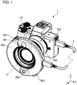
- FIG. 1 is an exterior perspective view of the camera system 1.
- an X axis and a Z axis that perpendicularly intersect one another will be defined on a bottom surface of the camera 100, and an axis that perpendicularly intersects the X axis and the Z axis will be defined as a Y axis.
- the direction of an optical axis O of the camera 100 is a direction parallel to the Z axis, and an object side will be defined as a front side.
- the side that is closer to the optical axis O in a radial direction from the optical axis O of the lens device 200 at the center will be defined as an inner peripheral side or the inside in the radial direction while the side away from the optical axis will be defined as an outer peripheral side or the outside in the radial direction.
- the lens device 200 is provided on the front surface of the camera 100.
- the distance detection device 300 is attached at a position at which it surrounds a periphery (outer periphery) of the lens device 200 with an attachment mechanism (not illustrated) at an end (front end) of the lens device 200 on the object side.
- the lens device 200 may be attached to and detached from a main body of the camera 100, or both the lens device 200 and the camera 100 may be integrally configured.
- the distance detection device 300 can be attached to or detached from the lens device 200 or is configured integrally with the lens device 200.
- the distance detection device 300 is attached such that the central axis thereof substantially conforms to the optical axis O of the imaging optical system included in the lens device 200. Therefore, the term "optical axis O" used for description in regard to the distance detection device 300 below can appropriately be interpreted as equivalent to the central axis of the distance detection device 300.
- the distance detection device 300 has an annular shape around the optical axis O at the center and includes a light emitting unit 301 and a light receiving unit 302. A front lens of the lens device 200 is exposed forward from an opening of the distance detection device 300.
- the distance detection device 300 is electrically connected to the camera 100 via a cable 2 and performs communication of various kinds of information and power supply.
- the distance detection device 300 is disposed to surround the periphery of the front end of the lens device 200, vignetting due to an obstacle such as the lens device 200 does not occur in irradiation light (distance measurement light) of the distance detection device 300. Irradiation is performed in an image angle region of the imaging apparatus, and the distance measurement light is received by an imaging unit for acquiring a distance image, thereby obtaining a distance image.
- the distance image is an image representing distance information indicating the distance between the camera 100 and the object.
- Fig. 2 is an exploded perspective view of the distance detection device 300.
- the distance detection device 300 includes a front cover 304, a light emitting unit 301, a light receiving unit 302, a flexible printed circuit (hereinafter abbreviated to FPC) 306, a connection terminal 307, attachment mechanisms 303, and a rear cover 305.
- FPC flexible printed circuit
- the light emitting unit 301 irradiates a target region with irradiation light.
- the light emitting unit 301 includes a light emitting element 309.
- the light receiving unit 302 includes a light receiving element (TOF sensor) 310 and a lens unit 308.
- the lens unit 308 includes an image formation lens disposed on the front surface side of the light receiving element 310, that is, on the side of the object that is a target in the target region.
- the light emitting element 309, the light receiving element 310, and a control IC (TOF-CPU) 350 are electrically connected to the FPC 306.
- the control IC (TOF-CPU) 350 controls the light emitting element 309 and the light receiving element 310.
- the connection terminal 307 is mounted on the FPC 306 and is exposed to the outside at a boundary between the front cover 304 and the rear cover 305 in a state in which the front cover 304 and the rear cover 305 are fastened and secured to each other with a screw or the like.
- the attachment mechanisms 303 function as detachable units used by the distance detection device 300 to be attached to and detached from the lens device 200. It is possible to perform attachment between the lens device 200 and the distance detection device 300 by sliding an operation lever that is an operation member in the attachment mechanisms 303.
- Fig. 3 is a block diagram illustrating a main electrical configuration of the camera system 1 according to the embodiment. First, configurations of the camera 100 and the lens device 200 will be described.
- the camera 100 has an MPU 101 to a diaphragm device 206.
- the MPU 101 executes various kinds of processing and instructions for various components.
- the MPU 101 has a one-chip IC circuit configuration with a built-in microcomputer including a central processing unit (CPU), a read only memory (ROM), a random access memory (RAM), an input/output control circuit (I/O CONTROL), a multiplexer, a timer circuit, and the like.
- the MPU 101 can control the camera system 1 using software.
- a battery 102 is a power source of the camera 100 and is connected to a power source circuit 103.
- the power source circuit 103 supplies an output voltage to each circuit, which will be described later.
- a switch group 106 includes a switch (SW1) that is turned on through a half-pressing operation of a release button 118, for example, and a switch (SW2) that is turned on through a full-pressing operation of the release button 118. Also, the switch group 106 includes various operation switches such as switches for setting exposure (a diaphragm and a shutter speed setting SW). Signals from the switch group 106 are acquired by the MPU 101.
- a distance measurement circuit 108 measures the object distance and outputs measurement data to the MPU 101.
- a method for measuring the object distance it is possible to acquire object distance information by emitting light for irradiation from the side of the camera 100 and receiving reflected light from the object in an active scheme, for example.
- an active scheme it is possible to detect object distance information by reading an image signal from an imaging sensor such as a line sensor or the like provided in a manner corresponding to a screen and performing an arithmetic operation in a phase difference detection scheme from a focal point position corresponding to an object image.
- the distance measurement circuit 108 can perform detection of feature regions such as face detection and pupil detection in a case in which the object is a person.
- the MPU 101 performs communication with the lens device 200 via a camera-side contact point 116 and a lens-side contact point 207.
- a lens control circuit 201 included in the lens device 200 performs communication with the MPU 101, drives an imaging lens 205 via an autofocus (AF) drive circuit 203, and performs focal point adjustment.
- AF autofocus
- Fig. 3 illustrates only one imaging lens 205 for convenience, the imaging optical system is actually configured of a group of multiple lenses such as a focus lens.
- the AF drive circuit 203 includes a stepping motor, for example, and changes the position of the focus lens in response to a control command from the lens control circuit 201, thereby adjusting a focal point.
- the lens control circuit 201 drives the diaphragm device 206 via a diaphragm drive circuit 204, thereby controlling exposure.
- the diaphragm drive circuit 204 includes an autoiris, for example, and changes an aperture diameter of the diaphragm device 206 in response to a control command from the lens control circuit 201, thereby optically adjusting a diaphragm value.
- a focal point distance detection circuit 109 included in the main body of the camera 100 outputs focal point distance information of the imaging lens 205 to the MPU 101.
- the imaging lens 205 is a single-focal-point lens
- data indicating a fixed focal point distance is sent to the MPU 101.
- the imaging lens 205 is a zoom lens
- data indicating a focal point distance in accordance with a zooming stop position of the imaging lens 205 detected by a zoom encoder (not illustrated) is sent to the MPU 101.
- a display unit 110 includes a display device such as a liquid crystal display (LCD), a liquid crystal view finder (EVF), or an organic EL display and displays information regarding image capturing, image information, and the like. Note that an organic EL or the like is used for the display unit 110.
- LCD liquid crystal display
- EVF liquid crystal view finder
- organic EL organic EL
- a shutter 114 is provided on the front surface side of an imaging element 113 and can move to a position at which the imaging element 113 is brought into a light blocking state and a position at which the imaging element 113 is brought into an exposure state.
- An image sensor using a charge coupled device (CCD) or a complementary metal oxide semiconductor (CMOS) is used for the imaging element 113 and outputs an image signal in accordance with a light flux received at the time of exposure through photoelectric conversion. In this manner, the object is imaged.
- CCD charge coupled device
- CMOS complementary metal oxide semiconductor
- a cable 2 is a connection member configured to connect a connection terminal 115 on the side of the camera main body to a connection terminal 307 on the side of the distance detection device 300.
- the MPU 101 and the TOF-CPU 350 perform mutual communication via the cable 2, the connection terminal 115, and the connection terminal 307, and power can be supplied from the camera main body to the distance detection device 300.
- the connection terminal 307 is a first communication unit configured to communicate various kinds of information (for example, distance information) to the camera 100 while the connection terminal 115 is a second communication unit configured to communicate various kinds of information to the distance detection device 300.
- the camera main body includes the battery 102 in the embodiment, a configuration in which the distance detection device 300 is also provided with a battery may be employed.
- the distance detection device 300 has the light emitting unit 301 to a posture detection unit 353.
- the light emitting unit 301 has the light emitting element 309.
- the light receiving unit 302 has the light receiving element 310 and a lens unit 308.
- the TOF-CPU 350 controls the entire distance detection device 300.
- the light emitting unit 301 is electrically connected to a light source drive unit 351, and the light source drive unit 351 causes the light emitting element 309 to emit light in response to a control signal from the TOF-CPU 350.
- a light emitting diode (LED), a vertical cavity surface emitting laser (VCSEL), or the like is typically used for the light emitting element 309, and a wavelength region of light to be used is a region of invisible light such as near-infrared light.
- An object 356 is a target in the irradiation target region.
- the irradiation light 354 is reflected by the object 356, and reflected light 355 thereof is received by the light receiving unit 302.
- the light receiving unit 302 includes the lens unit 308 and the light receiving element 310. After an image of the reflected light 355 from the object 356 is formed at the lens unit 308, the light receiving element 310 receives the light, performs photoelectrical conversion, and outputs an analog signal for generating a distance image.
- the analog signal output by the light receiving element 310 is acquired and converted into a digital signal by an A/D converter 352.
- the digital signal is transmitted to the TOF-CPU 350.
- the posture detection unit 353 includes a level function such as an angular speed sensor, an acceleration sensor, or an inclination sensor, detects posture information of the distance detection device 300, and outputs the detection signal to the TOF-CPU 350. It is possible to adjust attachment between the camera 100 and the distance detection device 300 on the basis of the posture information.
- a level function such as an angular speed sensor, an acceleration sensor, or an inclination sensor
- Distance detection using the light emitting unit 301 and the light receiving unit 302 is performed by the TOF-CPU 350 transmitting a control signal to each part in response to a command from the MPU 101 of the camera 100.
- the display unit 110 performs, on the screen, first live view display using the imaging element 113 of the camera 100 and second live view display using the light receiving element 310 of the distance detection device 300.
- the live view display performed by the distance detection device 300 it is possible to change a display state and display details by stopping irradiation of the object from the light emitting element 309 or adjusting the amount of irradiation with the irradiation light 354.
- a method for displaying an image using the display unit 110 As a method for displaying an image using the display unit 110, a method of displaying the first live view display and the second live view display in two split screens and a method of displaying the display images in a superimposed manner are exemplified. Alternatively, there is a method of arbitrarily selecting and displaying either the first live view display or the second live view display or the like.
- the TOF-CPU 350 transmits the digital signal acquired from the A/D converter 352, that is, a signal corresponding to the distance image data, to the MPU 101 via the connection terminal 307 on the side of the distance detection device, the cable 2, and the connection terminal 115 on the side of the camera.
- the MPU 101 acquires an image captured by the camera 100 and a distance image captured by the distance detection device 300 and performs image processing thereon.
- the MPU 101 generates data of a three-dimensional image by performing synthesis processing of the captured image and the distance image and saves the data in a recording device (not illustrated).
- saving methods a method of saving the three-dimensional image data after the synthesis, a method of applying the distance image to the captured image and saving the data, a method of separately saving each of the data of the captured image and the distance image, and the like are exemplified.
- Fig. 4A is a diagram for explaining the TOF system.
- the light emitting element 309 generates the irradiation light 354 modulated at 10 MHz, for example, and irradiates the object 356 therewith in response to a control signal from the TOF-CPU 350.
- An image of the reflected light 355 from the object 356 is formed by the lens unit 308, and the light reaches the light receiving element 310 with a delay time in accordance with the distance to the object 356.
- the TOF-CPU 350 calculates the distance from the camera system 1 to the object 356 on the basis of the delay time (TOF scheme).
- the TOF-CPU 350 calculates (acquires) the distance information on the basis of a time until the light receiving unit 302 receives the reflected light after the light emitting unit 301 emits the irradiation light for irradiation.
- FIG. 4B is a drawing that shows the distance between the distance detection device 300 and the imaging element 113 of the camera 100.
- the object distance 357 that has been acquired by the distance detection device 300 is set to distance information L.
- the distance information L serves as the distance up to the lens unit 308, actually, this is the distance to the receiving element 310.
- the distance detection device 300 is attached to the front end portion of the lens device 200, and thus, the imaging element 113 and the lens unit 308 of the camera 100 are attached at a distance separated only by 1 (small letter "1") units in the irradiation light axis direction.
- the lens device 200 stores the position information for the distance detection unit 300, and when the lens device 200 is attached to the camera 100, the MPU 101 acquires the distance information 1 (projection amount information).
- the MPU 101 based on the distance information L that has been acquired by the distance detection device 300, the MPU 101 records the distance 1 from the imaging element 113 to the lens unit 308 as a correction value, and the MPU 101 records this as the distance information L+1 for the distance to the object, where the distance information L+1 is the distance information L to which the distance 1, which is the correction value, has been added.
- the distance 1, which is the correction value is changed by the position information for the lens device 200 after the replacement.
- the MPU 101 detects that the lens device 200 has been replaced, and records the distance 1, which is a correction value, in the memory as a correction value by acquiring the position information for the distance detection device 300.
- the distance detection device 300 moves forward and backward accompanying the advancement to and retraction in the irradiation light axis direction O.
- FIG. 4C is a figure in which the distance detection device 300 has moved to the object 356 side by only ⁇ 1.
- the MPU 101 adds the movement amount ⁇ 1 of the distance detection device 300 to the distance information 1, and records this as distance information 1+ ⁇ 1.
- this is recorded as distance information 1- ⁇ 1. Therefore, the MPU 101 is linked to the zoom operation and the focus action, and continuously acquires the movement amount ⁇ 1 (movable amount).
- Fig. 5 is a diagram for explaining a captured image and a distance image acquired by the camera system 1.
- Fig. 5A illustrates a state of the distance detection device 300 when seen from the front side.
- the distance detection device 300 includes the light emitting element 309 and the light receiving element 310 illustrated in Fig. 5A , for example.
- Fig. 5B illustrates an image 358 captured by the camera 100.
- Fig. 5C illustrates a distance image 359 captured by the distance detection device 300.
- Fig. 5C represents an object distance acquired by the TOF system using concentration of white and black.
- the object distance is precisely acquired in the vicinity of the center of an image angle corresponding to a face part (feature region) of a person as an object. Precision of acquiring the object distance differs depending on the distance between the irradiation range of the light emitting element 309 and the object. Since the peripheral part in the vicinity of the center of the image angle is outside the irradiation range of the light emitting element 309, the precision of acquiring the object distance is poor.
- a map representing the object distance corresponding to the feature region of the object will be called an object distance map 364.
- the distance detection device 300 is disposed at the distal end of the lens device 200. Therefore, the irradiation light 354 from the light emitting unit 301 is not blocked by the camera 100 and the lens device 200 (no vignetting occurs) in the process before reaching the object. Similarly, the reflected light 355 from the object 356 is not blocked by the camera 100 and the lens device 200 in the process before reaching the light receiving unit 302. Also, the camera system 1 can output a three-dimensional image with a spatial effect by synthesizing the captured image and the distance image obtained with precision. In a case in which the captured image 358 illustrated in Fig. 5B and the distance image 359 illustrated in Fig. 5C are synthesized, for example, it is possible to acquire an image of the face part of the person that can be acquired by the object distance map 364 expressed in three dimensions (an embossing degree or the like).
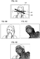
- Fig. 6 is a diagram for explaining a method of adjusting a position of attachment of the distance detection device 300 to the camera 100.
- deviation in the rotation direction around the optical axis O at the center may occur between captured image angles of the image captured by the camera 100 and the distance image captured by the distance detection device 300. If the image captured by the camera 100 and the distance image captured by the distance detection device 300 are synthesized in this case, images with different capture image angles overlap one another, and it is thus difficult to acquire a three-dimensional image.
- a method of adjusting the position for curbing or correcting deviations that may occur when the distance detection device 300 is attached will be described.
- Fig. 6A illustrates a state in which a live view image is displayed on the display unit 110 such as an LCD or a liquid crystal view finder (EVF) that the camera 100 has, which is not illustrated.
- the MPU 101 that the camera 100 has displays horizontal/vertical reference lines 361 on the display unit 110 in an overlapping manner on the live view image that is being displayed on the display unit 110.
- the horizontal/vertical reference lines 361 are, for example, grid lines or lines that perpendicularly intersect the optical axis O.
- the MPU 101 acquires posture information of the distance detection device 300 detected by the posture detection unit 353 of the distance detection device 300 from the distance detection device 300 via the connection terminal 307 and the connection terminal 115. Also, the MPU 101 displays a bar 360 indicating the acquired posture information in an overlapping manner on the live view image. In this manner, a person who captures the image can easily recognize how much the distance detection device 300 deviates in the rotation direction around the optical axis O at the center. Also, the person who captures the image can adjust the position of the attachment of the distance detection device 300 to the camera 100 while viewing the reference lines 361 and the bar 360 displayed on the display unit 110.
- the MPU 101 displays the posture of the distance detection device 300 using the bar 360 in the example illustrated in Fig. 6A
- another display method can be applied as long as the person who captures the image can recognize the inclination of the distance detection device 300 with respect to the reference lines 361.
- the posture detection unit 353 is preferably disposed at a position away from the optical axis O inside the distance detection device 300 for enhancing detection precision.
- Fig. 6B illustrates a live view image of a captured image that the camera 100 is capturing.
- Fig. 6C illustrates a live view image of a distance image that the distance detection device 300 attached to the camera 100 with deviation in the rotation direction around the optical axis O at the center by a predetermined amount is capturing.
- Fig. 6D illustrates a state in which the live view images are displayed on the display unit 110 of the camera 100.
- the MPU 101 displays the live view image of the distance image illustrated in Fig. 6C in an overlapping manner on the live view image of the captured image illustrated in Fig. 6B on the display unit 110.
- the person who captures the image can easily recognize how much the distance detection device 300 deviates in the rotation direction around the optical axis O at the center.
- the person who captures the image can adjust the position of the attachment of the distance detection device 300 to the camera 100 while viewing the live view image of the captured image and the live view image of the distance image displayed on the display unit 110.
- the MPU 101 extracts an edge portion of the captured image illustrated in Fig. 6B and an edge portion of the distance image illustrated in Fig. 6C .
- the edge portion of the captured image is, for example, a location where a color or a contrast of the object suddenly changes.
- the edge portion of the distance image is, for example, a location where distance information suddenly changes.
- the MPU 101 performs the correction such that the edge portions conform to each other by rotationally moving the distance image and displays the distance image in an overlapping manner with the captured image.
- the MPU 101 finishes the synthesized image as a three-dimensional image through cutting (trimming) since the distance image illustrated in Fig. 6C is inclined with respect to the captured image.
- Fig. 12 is an example of an exploded perspective view of the attachment mechanism 303.
- An attachment base 311 of the attachment mechanism 303 is screwed and secured to the front cover 304 using a screw 312.
- the attachment base 311 may be formed integrally with the front cover 304 or may be attached to the rear cover 305.
- a slider 313 that is a slide member is incorporated in the attachment base 311.
- the slider 313 is biased in a -Z direction with a spring 314 such that the slider 313 can operate in a direction parallel to the optical axis O relative to the attachment base 311 and performs a sliding operation relative to a rib of the attachment base 311, which is not illustrated.
- a plurality of step difference shaped portions are formed in the slider 313.
- the operation lever 315 is disposed at a position at which the slider 313 is sandwiched between the attachment base 311 and the operation lever 315.
- the operation lever 315 is biased in the radiation direction from the optical axis O, that is, outward in the radial direction of the distance detection device 300 with a spring 316 incorporated at a location of the attachment base 311, which is not illustrated.
- the operation lever 315 can perform an operation in the aforementioned radiation direction with the spring 316.
- the operation lever 315 is pinched between the front cover 304 and the rear cover 305 and can operate in the circumferential direction of an outer shape of the distance detection device 300.
- a slide blade 317 is disposed between the slider 313 and the operation lever 315 and is sandwiched between the attachment base 311 and a rib of the rear cover 305, which is not illustrated. Operations of the slide blade 317 will be described later.
- the slide blade 317 is formed into a thin plate shape and has a metal portion 317a. Also, the slide blade 317 has, for example, a rubber portion 317b as an end formed of a flexible member.
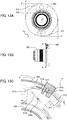
- Fig. 13 is a diagram illustrating a state before the distance detection device 300 is attached to the lens device 200.
- Fig. 13A illustrates a state when the distance detection device 300 is seen from the side of the optical axis O.
- the operation lever 315 In a state before the distance detection device 300 is attached to the lens device 200, that is, when the operation lever 315 is not operated, the operation lever 315 is disposed at a position extending further outward in the radial direction of the distance detection device 300 than the outer peripheral surface of the distance detection device 300.
- the distance detection device 300 illustrated in Fig. 13A is provided with a plurality of operation levers 315. Therefore, the distance detection device 300 has a plurality of attachment mechanisms 303 disposed at positions at which they face each other with the optical axis O sandwiched therebetween.
- Fig. 13B is a side view corresponding to Fig. 13A .
- Fig. 13C illustrates a section along the A-A line in Fig. 13B .
- the slide blade 317 is not in contact with the lens device 200.
- the operation levers 315 are biased with the spring 316 and are located at positions sticking out in a radiation direction E with reference to the optical axis O.
- notch portions 315a of the shafts of the operation levers 315 and a standing curved portion 317c of the slide blade 317 are fitted to each other.
- a cam hole 317d of the slide blade 317 slides with a sliding dowel 304a of the front cover 304.
- a locking portion 317e of the slide blade 317 that serves as a locked member and a first locking wall 313a of the slider 313 are in an abutting or approaching state.
- the locking portion 317e of the slide blade 317 is brought into contact and locked with the first locking wall 313a of the slider 313 even if the operation lever 315 is operated in a circumferential direction F (the clockwise direction in Fig. 13C ) of the distance detection device 300.
- the rotation of the operation lever 315 is restricted, and the operation lever 315 cannot move in the peripheral direction around the optical axis O at the center.
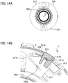
- Figs. 14 to 16 illustrate a state of the distance detection device 300 when the operation lever 315 is operated.
- Fig. 14A illustrates a state of the distance detection device 300 when the person who captures the image presses the operation lever 315 in a direction opposite to the radiation direction E.
- the operation lever 315 When the operation lever 315 is pressed, the operation lever 315 operates to enter the inside of the distance detection device 300.
- Fig. 14B illustrates a section in the state in Fig. 14A . If the person who captures the image presses the operation lever 315 in a direction against a bias force of the spring 316 (-E direction), the notch portion 315a operates along the standing curved portion 317c of the slide blade 317. At this time, an oblique surface portion 315b of the operation lever 315 is brought into contact with an oblique surface portion 313b of the slider 313, and the slider 313 moves in the Z direction as illustrated in Figs. 15A and 15B .
- Fig. 16 illustrates a state of the distance detection device 300 when the person who captures the image performs an operation of rotating the operation lever 315 in the circumferential direction F while pressing the operation lever 315.
- Fig. 16A if the person who captures the image performs the operation of rotating the operation lever 315 in the circumferential direction F, the slide blade 317 operates on the inner peripheral side of the distance detection device 300, that is, the direction toward the lens device 200.
- Fig. 16B illustrates a section of the attachment mechanism 303 after the operation of rotating the operation lever 315. If the slide blade 317 moves to the position illustrated in Fig. 16B , the lens device 200 is pinched with the rubber portion 317b of the slide blade 317. In this manner, it is possible to retain the distance detection device 300 secured to the lens device 200.
- the notch portion 315a of the operation lever 315 and the standing curved portion 317c of the slide blade 317 operate in a conjunctive manner. If the slide blade 317 moves in the circumferential direction F, the sliding dowel 304a of the front cover 304 and the cam hole 317d slide, and the slide blade 317 moves toward the lens device 200 (in the -E direction).
- the rubber portion 317b of the slide blade 317 is pressed against a groove portion 200a of the lens device 200.
- the attachment mechanisms 303 are disposed at two locations at which they face each other with the optical axis O sandwiched therebetween, and the distance detection device 300 pinches the lens device 200 and is secured by the rubber portion 317b being pressed against the groove portion 200a of the lens device 200.
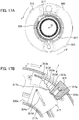
- Fig. 17 is a diagram illustrating a state of the distance detection device 300 when the person who captures the image releases the operation lever 315 from the state in Fig. 16A , that is, when the operation lever is not pressed (non-operation time).
- the operation lever 315 is brought into a state in which the operation lever 315 is sticking out in the E direction from the outer peripheral surface of the distance detection device 300 as illustrated in Figs. 17A and 17B .
- the slide blade 317 holds the state illustrated in Fig. 16 , and the distance detection device 300 is thus secured to the lens device 200.
- Fig. 17B illustrates a section of the attachment mechanism 303 in the state in Fig. 17A .
- the operation lever 315 is pushed to the side of the outer shape of the distance detection device 300 due to a bias force of the spring 316 while the notch portion 315a and the slide blade 317 slide.
- the operation lever 315 moves to the position in Fig. 17B , the state in which the slider is biased in the Z direction by the operation lever 315 is released. Therefore, the locking portion 317e of the slide blade 317 and the second locking wall 313c of the slider 313 are disposed in an abutting or approaching state. Thus, the slide blade 317 is locked, and the state in which the distance detection device 300 pinches the lens device 200 and is retained in a secured manner can be maintained.
- the distance detection device 300 Even if it is attempted to rotate the operation lever 315 in the circumferential direction F, the state in which the distance detection device 300 retains the lens device 200 in a secured manner is maintained due to engagement between the sliding dowel 304a and the cam hole 317d and abutting between the locking portion 317e and the second locking wall 313c. Also, since the slide blade 317 is fitted into the groove portion 200a of the lens device 200, the distance detection device 300 does not unexpectedly move.
- the distance detection device 300 is retained by the lens device 200 in a secured manner.
- the state in which the distance detection device 300 pinches the lens device 200 can be maintained with a third locking wall 313d, a fourth locking wall 313e, or a fifth locking wall 313f instead of the second locking wall 313c.
- the second locking wall 313c to the fifth locking wall 313f are formed as walls at different angles.
- the planes formed by the second locking wall 313c to the fifth locking wall 313f have angles in accordance with the position of the slide blade 317. Note that the angle of the plane that forms the first locking wall 313a may be set to be different from the angles of the planes forming the other locking walls.
- the operation lever 315 is disposed at the position sticking outward in the radial direction from the outer periphery of the distance detection device 300 for the following reason.
- the operation lever 315 is disposed on the front surface side (the side of the front cover 304) of the distance detection device 300, a hand or the like of the person who captures the image may be blocked by the lens device 200 when the person who captures the image operates the operation lever 315.
- the operation lever 315 is suitably disposed at the position sticking outward in the radial direction of the distance detection device 300.
- the operation lever 315 is disposed in a region surrounded by an outer diameter arc of the distance detection device 300, a first tangent line at a first point, and a second tangent line at a second point on the outer periphery of the distance detection device 300.
- the first tangent line and the second tangent line perpendicularly intersect one another.
- the aforementioned outer diameter arc is an outer diameter arc from the first point to the second point.
- the first tangent line is a tangent line X' in the X direction while the second tangent line is a tangent line Y' in the Y direction.
- the operation lever 315 is not brought into a direct contact with the desk, and the locking of the attachment mechanisms 303 is not unexpectedly released.
- Fig. 18 is a diagram illustrating a configuration example of the distance detection device 300 adapted in consideration of heat generation of the light emitting unit 301 and the light receiving unit 302.
- the light emitting element 309 and the light receiving element (TOF sensor) 310 disposed in the distance detection device 300 may serve as heat generation sources and these may affect detection precision and operations of the distance detection device 300.
- the light emitting unit 301 including the light emitting element 309 and the light receiving unit 302 including the light receiving element (TOF sensor) 310 will be defined as heat generation sources.
- Fig. 18A illustrates a state of the distance detection device 300 from which the front cover 304 has been removed when seen from the front side.
- the FPC 306 that is a circuit board in the distance detection device 300 includes the light emitting unit 301, the light receiving unit 302, and the connection terminal 307.
- the FPC 306 is disposed along the side of the rear cover 305, the FPC 306 may be disposed on the side of the front cover 304.
- the light emitting element 309 in the light emitting unit 301, the light receiving element (TOF sensor) 310 in the light receiving unit 302, and the connection terminal 307 are mounted on the FPC 306.
- the light emitting unit 301 and the light receiving unit 302 are disposed on the Y axis with the optical axis O at the center.
- the distance from the light emitting unit 301 to the light receiving unit 302 is defined as a distance H1.
- the distance from the optical axis O, that is, the central axis of the distance detection device to the light emitting unit 301 is defined as a distance H2.
- the light emitting unit 301 and the light receiving unit 302 are disposed such that the distance H1 is longer than the distance H2. Since the light emitting unit 301 and the light receiving unit 302 that are heat generation sources are located at a far distance in the configuration illustrated in Fig. 18A , it is possible to curb a local temperature rise in the distance detection device 300.
- the light emitting unit 301 and the light receiving unit 302 may not be disposed on the Y axis with the optical axis O at the center. Even in a case in which the light emitting unit 301 and the light receiving unit 302 cannot be disposed on the Y axis, it is only necessary to set the distance H1 from the light emitting unit 301 to the light receiving unit 302 to be longer than the distance H2 from the optical axis O to the light emitting unit 301.
- the distance H1 it is possible to set the distance H1 to be longer than the distance H2 in the distance detection device 300 by disposing the light emitting unit 301 and the light receiving unit 302 at positions at which they face one another with the optical axis O sandwiched therebetween in a plane that perpendicularly intersects the optical axis O.
- connection terminal 307 is disposed at an intermediate position between the light emitting unit 301 and the light receiving unit 302 disposed on the FPC 306. Therefore, the FPC 306 is branched into two parts toward the light emitting unit 301 and the light receiving unit 302 when seen from the connection terminal 307. With this configuration, it is possible to curb a temperature rise due to heat transmitted from the light emitting unit 301 and the light receiving unit 302 in relation to the connection terminal 307 exposed to the exterior of the distance detection device 300. Note that the position of the connection terminal 307 is not limited to the intermediate position between the light emitting unit 301 and the light receiving unit 302 on the FPC 306.
- Fig. 18B illustrates an example of disposition of the connection terminal 307 in the distance detection device 300.
- the distance from the light emitting unit 301 to the connection terminal 307 is defined as a distance H3.
- the distance from the light receiving unit 302 to the connection terminal 307 is defined as a distance H4.
- the connection terminal 307 is disposed such that the distance H3 is longer than the distance H4. Therefore, the connection terminal 307 illustrated in Fig. 18B is disposed closer to the side of the light receiving unit 302 as compared with the connection terminal 307 illustrated in Fig. 18A . With such a configuration, it is possible to curb a temperature rise at the connection terminal 307 even if the light emitting unit 301 includes the light emitting element 309 with high heat generating properties with respect to the light receiving unit 302.
- connection terminal 307 is disposed on the side of the light emitting unit 301.
- connection terminal 307 of the distance detection device 300 is preferably connected to the connection terminal 115 of the camera 100 at a shortest distance with the cable 2.
- the connection terminal 307 of the distance detection device 300 is disposed in the same direction as that of the connection terminal 115 of the camera 100 with reference to the optical axis O in a plane that perpendicularly intersects the optical axis O.
- Fig. 18C illustrates an example in which a heat countermeasure member 330 is disposed in the distance detection device 300.
- a heat dissipating member such as a metal plate made of metal such as copper or aluminum or a graphite sheet is used.
- the heat countermeasure member 330 is disposed at a position at which it faces the FPC 306 (a facing position with reference to the Y axis) with the optical axis O, that is, the central axis of the distance detection device 300, sandwiched therebetween.
- the attachment position of the heat countermeasure member 330 is not limited to the position illustrated in Fig. 18C .
- the heat countermeasure member 330 may be disposed in substantially the same plane as that of the FPC 306. With such a configuration, it is possible to dispose the heat countermeasure member 330 without increasing the thickness of the distance detection device 300 in the Z-axis direction. In the configuration example illustrated in Fig.
- the heat countermeasure member 330 is disposed at the position that faces the disposition position of the connection terminal 307 with the optical axis O sandwiched therebetween, and it is thus possible to curb a temperature rise in the connection terminal 307 as compared with the configuration example illustrated in Fig. 18B .
- the FPC 306 and the heat countermeasure member 330 have substantially equivalent lengths in Fig. 18C , it is not necessary for the FPC 306 and the heat countermeasure member 330 to have equivalent lengths.
- the distance detection device 300 may have a plurality of heat countermeasure members 330.
- the heat countermeasure member 330 in Fig. 18C is disposed so as to connect the light emitting unit 301 to the light receiving unit 302, the heat countermeasure members 330 may be disposed in each of the light emitting unit 301 and the light receiving unit 302.
- Figs. 19 and 20 are diagrams for explaining an example of a signal wiring provided on the FPC 306.
- Fig. 19 illustrates a plan view of the signal wiring provided on the FPC 306.
- Fig. 20 illustrates a sectional view of the FPC 306.
- Fig. 20A illustrates a section along the S1-S1 line in Fig. 19 while
- Fig. 20B illustrates a sectional along the S2-S2 line in Fig. 19 .
- a light emitting signal wiring 721b that is a first signal wiring electrically connects the light emitting element 309 to the connection terminal 307.
- An analog signal for driving the light emitting element 309 from the light source drive unit 351 ( Fig. 3 ) is transmitted to the light emitting element 309 via the light emitting signal wiring 721b.
- the analog signal for driving the light emitting element 309 includes a modulation signal for modulating the irradiation light 354 from the light emitting element 309 at high frequency, for example.
- light receiving signal wirings 721c and 721d that are second signal wirings electrically connect the light receiving element 310 to the connection terminal 307.
- An analog signal output from the light receiving element 310 is converted into a digital signal by the A/D converter 352 (illustrated in Fig. 3 ) and is transmitted to the connection terminal 307 via the light receiving signal wirings 721c and 721d.
- the digital signal is transmitted as a distance image to the MPU 101 via the cable 2 and the connection terminal 115.
- the FPC 306 includes an insulating layer 720, a first wiring layer 721 laminated and formed on one surface of the insulating layer 720, and a second wiring layer 722 laminated and formed on the other surface of the insulating layer 720.
- a GND wiring 721a and a pair of light receiving signal wirings 721c and 721d are arranged in the first wiring layer 721.
- the GND wiring 721a is arranged in the second wiring layer 722 as well.
- the light emitting signal wiring 721b is also arranged in the first wiring layer 721 as illustrated in Fig. 20B .
- the first wiring layer 721 and the second wiring layer 722 are covered with a cover lay 723 that is an insulating member to protect the GND wiring 721a, the light emitting signal wiring 721b, the light receiving signal wirings 721c and 721d.
- the light receiving signal wirings 721c and 721d are surrounded by the GND wiring 721a from their sides in the first wiring layer 721 and are also surrounded from their lower sides by the GND wiring 721a provided in the second wiring layer 722 via the insulating layer 720. Also, the light receiving signal wirings 721c and 721d are arranged in parallel, and gaps 724 are provided between the GND wiring 721a and the light receiving signal wirings 721c and 721d and between the light receiving signal wiring 721c and the light receiving signal wiring 721d. With the configuration described above, the light receiving signal wirings 721c and 721d form differential signal wirings. In this manner, a signal waveform interference (crosstalk) due to coupling of electromagnetic fields between the light receiving signal wirings 721c and 721d that are high-speed transmission signal wirings and the adjacent signal wirings is curbed.
- crosstalk due to coupling of electromagnetic fields between the light receiving signal wirings 721c and 721d that are high-speed transmission signal wirings and the adjacent signal
- the light emitting signal wiring 721b is arranged in a clockwise direction when seen from the front side of the distance detection device 300 (when seen from the -Z direction) from the light emitting element 309 toward the connection terminal 307.
- the light emitting signal wiring 721b is arranged on a wiring route of the line segment L6 (the route in the counterclockwise direction) illustrated in Fig. 19 is assumed.
- the light emitting signal wiring 721b passes through a position that faces the light receiving element 310 or the light receiving signal wirings 721c and 721d in the lamination direction of the FPC 306 with the insulating layer 720 sandwiched therebetween.
- the FPC 306 is enlarged in the lamination direction and the surface direction by the amount of separation in the arrangement of the light emitting signal wiring 721b, and the distance detection device 300 increases in size.
- the light emitting signal wiring 721b in the clockwise direction as illustrated in Fig. 19 , it is possible to arrange the light emitting signal wiring 721b without causing the light emitting signal wiring 721b to overlap the light receiving signal wirings 721c and 721d in the lamination direction of the FPC 306 and without causing the light emitting signal wiring 721b to be adjacent to the light receiving signal wirings 721c and 721d in the surface direction.
- the aforementioned configuration can prevent crosstalk from occurring between the light receiving signal wirings 721c and 721d and a light emitting element signal wirings 724 and acquire a distance image with precision.
- the distance detection device 300 Since the distance detection device 300 according to the embodiment described above is attached to the end of the lens device 200 on the object side, it is possible to acquire distance image information without allowing the irradiation light from the light emitting unit 301 to be blocked by the lens device 200.
- the distance detection device 300 may have a configuration other than the annular shape as long as the distance detection device 300 is disposed near the distal end of the lens device 200.
- Fig. 7 is a block diagram illustrating a main electrical configuration of a camera system 1.
- a light emitting unit 301 is provided with a plurality of light emitting elements 501A to 501H.
- a light source drive unit 351 drives the plurality of light emitting elements and causes each of the light emitting elements to irradiate an object with irradiation light 354 in response to a signal controlled by a TOF-CPU 350.
- the plurality of light emitting elements By disposing the plurality of light emitting elements in the light emitting unit 301 in this manner, it is possible to increase the irradiation range of the irradiation light 354 with respect to a captured image angle of a camera 100. Thus, it is also possible to irradiate the entire region of the captured image angle with the irradiation light 354 by taking the irradiation range of the light emitting elements and the number of disposed light emitting elements into consideration.
- each light emitting unit 301 irradiates the object with the irradiation light 354 from the light emitting elements at the same time, there may be a case in which precision of detection of distance information is degraded in a case in which the irradiation light 354 overlaps.
- each light emitting unit 301 may emit light at different timings instead of emitting light at the same time.
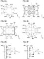
- Fig. 8 is a diagram for explaining disposition of the plurality of light emitting elements and the irradiation range of the irradiation light from the light emitting elements in the second embodiment.
- Fig. 8 illustrates a state when the distance detection device 300 in which the light emitting elements are disposed so as to emit irradiation light for irradiation in parallel to an optical axis O is seen from the front side.
- Fig. 8B illustrates an irradiation range of the irradiation light from the light emitting elements with respect to a captured image angle 500 of the camera 100 in the case of the disposition example illustrated in Fig. 8A .
- the light emitting elements 501A, 501B, 501C, 501D, 501E, 501F, 501G, and 501H are disposed at equal distances from the optical axis O and at equal intervals among the light emitting elements.
- irradiation ranges 501a to 501h correspond to the irradiation ranges of the light emitting elements 501A to 501H in Fig. 8A , respectively.
- the captured image angle 500 is typically short in the Y-axis direction due to a difference in aspect ratio of the imaging element 113 as illustrated in Fig. 8B . Therefore, the irradiation ranges 501a, 501d, 501e, and 501h of the light emitting elements 501A, 501D, 501E, and 501H disposed away from the optical axis O in the Y direction are likely to stick out from the captured image angle 500.
- Fig. 8C illustrates a state when the distance detection device 300 in which the light emitting elements are disposed so as to perform irradiation with an inclination at a predetermined angle with respect to the direction of the optical axis O is seen from a side.
- Fig. 8D illustrates irradiation ranges of the irradiation from the light emitting elements with respect to the captured image angle 500 of the camera 100 in the case of the disposition example illustrated in Fig. 8C .
- the light emitting elements in Fig. 8A are disposed with inclination at a predetermined angle with respect to the direction of the optical axis O.
- the light emitting element 502C and the light emitting element 502D will be described as an example.
- An angle between an irradiation light axis C of irradiation light from the light emitting element 502C with respect to the object and the optical axis O is defined as an angle ⁇ 1.
- an angle between an irradiation light axis D of irradiation light from the light emitting element 502D with respect to the object and the optical axis O is defined as an angle ⁇ 2.
- the irradiation light axis C and the irradiation light axis D are not parallel to the optical axis O.
- the light emitting elements 502C and 502D are disposed such that the angle ⁇ 2 is greater than the angle ⁇ 1.
- the first light emitting unit (light emitting element 502D) the distance of which from the central axis (optical axis O) of the distance detection device 300 in the vertical direction is a first distance, has greater inclination of the irradiation light axis than the second light emitting unit (light emitting element 502C), the distance of which from the central axis in the vertical direction is a second distance that is shorter than the first distance. In this manner, it is possible to cause the irradiation range 502d to be located on the center side of the captured image angle 500 as illustrated in Fig. 8D .
- the irradiation range 501c of the irradiation light from the light emitting element 501C less deviates in the Y-axis direction with respect to the captured image angle 500 than the irradiation range 501d. Therefore, the light emitting element 502C performs irradiation at the angle ⁇ 1 that is smaller than the angle ⁇ 2 corresponding to the irradiation light from the light emitting element 502D as illustrated in Fig. 8C .
- Fig. 8E illustrates a state when the distance detection device 300 in which a part of the plurality of light emitting elements is disposed to be closer to the optical axis O is seen from the front side.
- Fig. 8F illustrates a disposition example corresponding to Fig. 8E and illustrates a state in which the distance detection device 300 when the light emitting elements are disposed so as to perform irradiation with inclination at a predetermined angle with respect to the optical axis O is seen from a side.
- the positions of the light emitting elements 503B, 503C, 503F, and 503G are similar to the positions of the light emitting elements 501B, 501C, 501F, and 501G in Fig. 8A .
- the light emitting elements 503A, 503D, 503E, and 503H illustrated in Fig. 8E are disposed inward (inner circumferential side) in the radial direction of the distance detection device 300 so as to be closer to the optical axis O as compared with the light emitting elements 501A, 501D, 501E, and 501H illustrated in Fig. 8A .
- the angle between the irradiation light axis D' of the irradiation light from the light emitting element 503D with respect to the object and the optical axis O is defined as an angle ⁇ 3.
- the angle ⁇ 3 illustrated in Fig. 8F becomes an angle that is smaller than the angle ⁇ 2 between the irradiation light axis D of the irradiation light from the light emitting element 502D with respect to the object as illustrated in Fig. 8C and the optical axis O.
- the light emitting elements located further in the Y-axis direction from the optical axis O, such as the light emitting elements 503A, 503D, 503E, and 503H, inward in the radial direction of the distance detection device 300 such that the light emitting elements approach the optical axis O.
- the light emitting elements 503A, 503D, 503E, and 503H configured to irradiate the vicinity of the center of the captured image angle 500 emit irradiation light for irradiation first, and then the light emitting elements 503B, 503C, 503F, and 503G emit irradiation light for irradiation.
- the object near the center of the captured image angle 500 can be irradiated first by emitting the irradiation light from the light emitting elements in such an order, the person who captures the image fails to captures the object in fewer cases.
- the disposition of the light emitting elements with respect to the captured image angle 500 in relation to the Y-axis direction has been described, the same applies to the X-axis direction.
- Fig. 9 is a block diagram illustrating a main electrical configuration of a camera system 1 according to a third embodiment.
- the distance detection device 300 has a light emitting unit 301 that has a light emitting element and a scanning device of a MEMS scheme produced using a semiconductor process.
- the MEMS is an abbreviation of a micro-electro-mechanical system.
- the light emitting unit 301 is provided with a scanning device 400 of the MEMS scheme along with a light emitting element 309.
- the distance detection device 300 has a SUB-TOF-CPU 401 that serves as a control unit configured to cause a scanning device 400 to operate.
- the SUB-TOF-CPU 401 receives a control signal from a TOF-CPU 350 and drives the scanning device 400.
- a light source driving unit 351 causes the light emitting element 309 to emit light by the control signal from the TOF-CPU 350, and the emitted light is reflected by a reflection mirror 402 of the scanning device 400 to irradiate the object.
- the TOF-CPU 350 may directly control the scanning device 400 without providing the SUB-TOF-CPU 401.
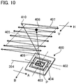
- Fig. 10 is a diagram for explaining a configuration of the scanning device 400 and a state in which the irradiation light 354 scanned by the scanning device 400 forms an irradiation range 405 in a two-dimensional manner.
- the reflection mirror 402 is formed at the center of the scanning device 400.
- the scanning device 400 has a so-called gimbal structure that has a torsion bar 403 for causing the reflection mirror 402 to swing around a vertical axis (B axis) and a torsion bar 404 for causing the reflection mirror 402 to swing around a horizontal axis (A axis).
- the scanning device 400 has an actuator that drives the reflection mirror 402 around the vertical axis (B axis) and uses an electromagnetic force, an electrostatic force, or the like, which is not illustrated, and the reflection mirror 402 swings at a high speed due to a resonance effect of the structure. Also, the scanning device 400 has an actuator that uses an electromagnetic force, an electrostatic force, or the like that causes the reflection mirror 402 to swing around the horizontal axis (A axis) in synchronization with the swinging around the vertical axis (B axis), which is not illustrated.
- the line 407 represents a going path of a light flux (scanning lines) scanned in the horizontal direction through the swinging of the reflection mirror 402 around the vertical axis (B axis), and the line 408 represents a coming path.
- the number of scanning lines is larger than that illustrated in Fig. 10 in practice, a smaller number of scanning lines are illustrated for easiness of explanation.
- the scanning device 400 further causes the reflection mirror 402 to swing around the horizontal axis (A axis) in synchronization of the swinging of the reflection mirror 402 in the vertical axis (B axis) and scans the scanning lines in the vertical direction (V direction) as well. If the scanning lines reach a scanning end 409 in the vertical direction, then the scanning lines are returned to a scanning start point 410. In this manner, it is possible to form the irradiation range 405 in a two-dimensional manner by the scanning device 400 causing the reflection mirror 402 to successively swing.
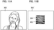
- Fig. 11 is a diagram illustrating a captured image and a distance image acquired in the third embodiment.
- Fig. 11A illustrates an image 362 captured by the camera 100. Also, Fig. 11B illustrates a distance image 363 captured by the distance detection device 300 including the light emitting unit 301 illustrated in Fig. 9 .
- the light emitting unit 301 irradiates the irradiation range 405 formed by the scanning device 400 causing the reflection mirror 402 to successively swing.
- the distance detection device 300 acquires an object distance map 364 near the center of an image angle corresponding to a face part of a person as an object. Therefore, it is possible to acquire an object distance with precision near the center of the image angle corresponding to the face part of the person.
- the camera system 1 synthesizes the captured image 362 illustrated in Fig. 11A with the distance image 363 illustrated in Fig. 11B , thereby obtaining an image expressing a three-dimensional shape (an embossing degree or the like) of the face part (object distance map 364) of the person, the distance image of which has been able to be acquired.
- the irradiation range is expanded through the driving of the scanning device 400, and the distance image 363 thus has a wider range of acquisition of corresponding distance information.
- the range of acquisition of the distance image 363 is determined by the type and the disposition of the light emitting unit 301 and the scanning range of the scanning device 400. It is possible to widen the irradiation range by using the light emitting unit 301 that has the light emitting element 309 and the scanning device 400 as in the third embodiment.
- An irradiation method in which an arbitrary range is selected within a captured image angle to set the irradiation range may be employed depending on the driving range of the scanning device 400.
- the light emitting unit 301 that has the light emitting element 309 and the scanning device 400 can typically use the light emitting element such as a laser with a smaller irradiation angle as compared with the light emitting unit that has only the light emitting element, it is possible to irradiate an object at a further location.
- a configuration provided with a plurality of combinations of the light emitting units 301 each having the light emitting element 309 and the scanning device 400 may be employed.
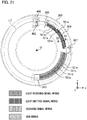
- Figs. 21 to 23 are diagrams for explaining signal wirings provided on the FPC 306 according to the third embodiment.
- Fig. 21 illustrates a plan view of the signal wirings provided on the FPC 306.
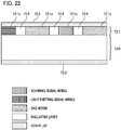
- Fig. 22 illustrates a section along the S3-S3 line in Fig. 21 . Note that the same reference signs will be applied to the same components as those in the first embodiment, and description thereof will be omitted in this embodiment.
- a scanning signal wiring 721e that is a third signal wiring electrically connects the scanning device 400 to the connection terminal 307.
- a rectangular pulse signal (digital signal) that is transmitted from the SUB-TOF-CPU 401 ( Fig. 9 ) for driving the scanning device 400 is transmitted to the scanning device 400 via the scanning signal wiring 721e.
- the first wiring layer 721 is covered with a cover lay 723 that is an insulating member to protect the GND wiring 721a, the light emitting signal wiring 721b, the light receiving signal wirings 721c and 721d, and the scanning signal wiring 721e.
- the light emitting signal wiring 721b and the light receiving signal wirings 721c and 721d are disposed so as not to overlap one another in the lamination direction of the FPC 306.
- the scanning signal wiring 721e is surrounded from its side by the GND wiring 721a in the first wiring layer 721, and the GND wiring 721a forms a guard GND wiring for the scanning signal wiring 721e.
- the light emitting signal wiring 721b, the GND wiring 721a, the scanning signal wiring 721e, and the GND wiring 721a are arranged in parallel in this order from the outer peripheral side of the rear cover 305.
- a gap 724 is provided between the wirings.
- the GND wiring 721a curbs signal leakage from the scanning signal wiring 721e, and crosstalk occurring between the scanning signal wiring 721e and the light emitting signal wiring 721b is curbed.
- the scanning signal wiring 721e is surrounded only from its side by the GND wiring 721a.
- the scanning signal wiring 721e may not only be surrounded from its side by the GND wiring 721a but also be surrounded from its lower side as well by the GND wiring 721a arranged in the second wiring layer 722 via the insulating layer 720.
- the light emitting signal wiring 721b is arranged in the clockwise direction when seen from the front side of the distance detection device 300 (when seen in the -Z direction) from the light emitting element 309 toward the connection terminal 307.
- the light emitting signal wiring 721b is arranged on a wiring route (a route in the counterclockwise direction) of the line segment L7 illustrated in Fig. 21 will be assumed.
- the light emitting signal wiring 721b passes the position that faces the scanning device 400 in the lamination direction of the FPC 306 with the insulating layer 720 sandwiched therebetween.
- crosstalk occurs between the scanning device 400 or the scanning signal wiring 721e and the light emitting element signal wiring 724. Therefore, precision of the amount of irradiation light emitted from the light emitting element 309 for irradiation is degraded, or precision of the swinging operation of the reflection mirror 402 included in the scanning device 400 is degraded.
- the distance detection device 300 As a result, precision of the distance image acquired by the distance detection device 300 is degraded.
- a method of arranging the light emitting signal wiring 721b so as to be separated from the scanning signal wiring 721e in the lamination direction and the surface direction of the FPC 306 is conceivable.
- the FPC 306 is enlarged in the lamination direction and the surface direction by the amount of the separation in the arrangement of the light emitting signal wiring 721b, and the distance detection device 300 increases in size.
- the scanning signal wiring 721e and the light receiving signal wirings 721c and 721d pass through the positions at which they face one another in the lamination direction of the FPC 306 similarly to the light emitting signal wiring 721b, crosstalk occurs between the scanning signal wiring 721e and the light receiving signal wirings 721c and 721d. Therefore, the scanning signal wiring 721e is arranged without overlapping the light receiving signal wirings 721c and 721d in the lamination direction of the FPC 306. It is only necessary for such an arrangement method to be carried out by replacing the light emitting signal wiring 721b with the scanning signal wiring 721e in the positional relationship between the light emitting signal wiring 721b and the light receiving signal wirings 721c and 721d illustrated in Figs. 19 and 20 , and detailed description will be omitted.
- a clock signal (not illustrated) for adjusting a timing of transmitting and receiving the distance image between the distance detection device 300 and the camera 100.
- a clock signal wiring is also one of high-speed signal wirings, and crosstalk occurring between the clock signal wiring and the light emitting signal wiring 721b is curbed by providing the guard GND wiring similarly to the scanning signal wiring 721e. It is only necessary for such an arrangement method to be carried out by replacing the scanning signal wiring 721e with the clock signal wiring in the positional relationship between the light emitting signal wiring 721b and the scanning signal wiring 721e illustrated in Figs. 21 and 22 , and detailed description will be omitted.
- Fig. 23 is a disposition example of the light emitting element 309 that cannot prevent crosstalk. Illustration of the FPC 306 is omitted.
- the distance detection device 300 there is a case in which it is not possible to prevent crosstalk between the light emitting signal wiring 721b and the light receiving signal wirings 721c and 721d or the scanning signal wiring 721e depending on the disposition of the light emitting element 309.
- the light emitting element 309 is disposed at a position further from the connection terminal 307 than the light receiving element 310 and the scanning device 400.
- the light emitting signal wiring 721b has to be arranged through the wiring route of the line segment L8 or the line segment L9 in order to electrically connect the light emitting element 309 to the connection terminal 307.
- the light emitting signal wiring 721b In a case in which the light emitting signal wiring 721b is arranged through the wiring route of the line segment L8, the light emitting signal wiring 721b passes through the position at which it faces the light receiving element 310 and the light receiving signal wirings 721c and 721d in the lamination direction of the FPC 306 with the insulating layer 720 sandwiched therebetween. In a case in which the light emitting signal wiring 721b is arranged on the wiring route of the line segment L9, the light emitting signal wiring 721b passes through a position at which it faces the scanning device 400 and the scanning signal wiring 721e in the lamination direction of the FPC 306 with the insulating layer 720 sandwiched therebetween. Therefore, it is not possible to prevent crosstalk between the light emitting signal wiring 721b and the light receiving signal wirings 721c and 721d or the scanning signal wiring 721e.
- the light emitting element 309 is disposed at a position closer to the connection terminal 307 than the light receiving element 310 and the scanning device 400 in the distance detection device 300 according to the embodiment illustrated in Fig. 21 .
- the light emitting signal wiring 721b does not pass through the position at which it faces the scanning device 400 and the scanning signal wiring 721e in the lamination direction of the FPC 306 with the insulating layer 720 sandwiched therebetween.
- the light emitting signal wiring 721b does not pass through the position at which it faces the light receiving element 310 and the light receiving signal wirings 721c and 721d in the lamination direction of the FPC 306 with the insulating layer 720 sandwiched therebetween as well.
- the distance detection device 300 illustrated in Fig. 9 may have a plurality of light emitting elements.
- Embodiment(s) of the present invention can also be realized by a computer of a system or apparatus that reads out and executes computer executable instructions (e.g., one or more programs) recorded on a storage medium (which may also be referred to more fully as a 'non-transitory computer-readable storage medium') to perform the functions of one or more of the above-described embodiment(s) and/or that includes one or more circuits (e.g., application specific integrated circuit (ASIC)) for performing the functions of one or more of the above-described embodiment(s), and by a method performed by the computer of the system or apparatus by, for example, reading out and executing the computer executable instructions from the storage medium to perform the functions of one or more of the above-described embodiment(s) and/or controlling the one or more circuits to perform the functions of one or more of the above-described embodiment(s).
- computer executable instructions e.g., one or more programs
- a storage medium which may also be referred to more fully as
- the computer may comprise one or more processors (e.g., central processing unit (CPU), micro processing unit (MPU)) and may include a network of separate computers or separate processors to read out and execute the computer executable instructions.
- the computer executable instructions may be provided to the computer, for example, from a network or the storage medium.
- the storage medium may include, for example, one or more of hard disk, a random-access memory (RAM), a read only memory (ROM), a storage of distributed computing systems, an optical disk (such as a compact disc (CD), digital versatile disc (DVD), or Blu-ray Disc (BD)TM), a flash memory device, a memory card, and the like.
- a distance detection device 300 attached to a position at which it surrounds a camera lens device (200).
- the distance detection device has a light emitting element (309) configured to irradiate a target region with irradiation light and a light receiving element (310) configured to receive reflected light of the irradiation light from a target in the target region.
- the distance detection device acquires distance information indicating a distance to the target on the basis of a time until the light receiving element receives the reflected light after the light emitting element performs irradiation with the irradiation light and communicates the distance information.
Landscapes
- Physics & Mathematics (AREA)
- General Physics & Mathematics (AREA)
- Engineering & Computer Science (AREA)
- Electromagnetism (AREA)
- Computer Networks & Wireless Communication (AREA)
- Radar, Positioning & Navigation (AREA)
- Remote Sensing (AREA)
- Optics & Photonics (AREA)
- Studio Devices (AREA)
- Optical Radar Systems And Details Thereof (AREA)
- Measurement Of Optical Distance (AREA)
- Focusing (AREA)
- Accessories Of Cameras (AREA)
- Automatic Focus Adjustment (AREA)
- Indication In Cameras, And Counting Of Exposures (AREA)
- Cameras Adapted For Combination With Other Photographic Or Optical Apparatuses (AREA)
Abstract
Description
- The present invention relates to a distance detection device configured to acquire distance information of an object.
- With the spread of smartphones and the like, opportunities for imaging and the number of photos taken have significantly increased, and image quality and a sense of resolution of captured images have improved with the advancement of peripheral technologies. In order to further enhance image quality and a sense of resolution, there is a technology of acquiring distance information (image depth information) from an imaging apparatus to an object for each pixel. It is possible to acquire the distance information before image capturing, to thereby increase a speed of automatic focus adjustment (AF), to perform image capturing assistance such as complementing of locations where blown out highlights, blocked out shadows, and the like have occurred, and to perform three-dimensional image expression of two-dimensional images. It is possible to use the distance information at the time of image capturing to set a contrast difference between a background and an image of a main object, to emphasize an outline of the main object, and to adjust shading generated by external light directed to the main object. It is possible to use the distance information retained at the time of image capturing to perform image processing to change the direction of the external light, with which the main object is irradiated, and to perform the aforementioned complementing after the image capturing. Also, the distance information is used for three-dimensional space mapping in the fields of multi-view imaging, augmented reality, virtual reality, and the like. A distance image for acquiring distance information from an image or a video is an image representing distance information of the object for each pixel.
- The time of flight (TOF) scheme is a method of performing irradiation with distance measurement light from an imaging apparatus toward an object and calculating the distance on the basis of a time required by an imaging element for acquiring a distance image to receive the reflected light thereof. For example, an object is irradiated with infrared light with intensity modulated in a predetermined irradiation pattern. The infrared light reflected by the object is received by the imaging element, and a time difference between a timing of the irradiation in the irradiation pattern and a timing of the light reception is detected, and thereby a distance value is calculated. The distance value is collected in a bit map manner for each pixel and is saved as distance image data. The apparatus disclosed in Japanese Patent Laid-Open No.
2014-157044 -
Fig. 24 is a diagram illustrating an example of a side surface of an imaging apparatus with a distance measurement light irradiator disposed therein and a distance image. As illustrated inFig. 24A , an imaging apparatusmain body 100 is provided with a distancemeasurement light irradiator 301. In order to acquire a distance image, it is necessary fordistance measurement light 354 emitted from the distancemeasurement light irradiator 301 for irradiation to reach an object. If the distancemeasurement light irradiator 301 is disposed in the imaging apparatusmain body 100 in accordance with details disclosed in Japanese Patent Laid-Open No.2014-157044 distance measurement light 354 is blocked by alens barrel 200 provided in the imaging apparatusmain body 100 and does not reach the object (vignetting occurs). -
Fig. 24B illustrates adistance image 359 in a case in which thedistance measurement light 354 is blocked by thelens barrel 200. In a case in which a region that is not irradiated with thedistance measurement light 354 is present in an image angle region including the object, an imaging element for acquiring a distance image cannot receive thedistance measurement light 354 in the range of the region that is not irradiated. InFig. 24B , the region, which is not irradiated with thedistance measurement light 354, in which the distance image cannot be acquired, is illustrated as aregion 365. Theregion 365 is output as being at infinity. - The present invention provides a distance detection device and an imaging apparatus, it is possible to irradiate a target with irradiation light for detecting a distance to an object without allowing any configuration members such as a lens barrel included in the imaging apparatus to block the irradiation light.
- The present invention in its first aspect provides a distance detection device as specified
claims 1 to 31. The present invention in its second aspect provides an imaging apparatus as specified claims 32 to 35. - Further features of the present invention will become apparent from the following description of exemplary embodiments with reference to the attached drawings.
-
-
Fig. 1 is an exterior perspective view of a camera system. -
Fig. 2 is an exploded perspective view for explaining a distance detection device. -
Fig. 3 is a diagram for explaining a circuit configuration of the camera system. -
Figs. 4A, 4B and 4C are diagrams for explaining a TOF system. -
Figs. 5A, 5B and 5C are diagrams for explaining a captured image and a distance image. -
Figs. 6A, 6B, 6C, and 6D are diagrams for explaining a method for adjusting an attachment position of the distance detection device. -
Fig. 7 is a diagram for explaining a circuit configuration of the camera system. -
Figs. 8A, 8B, 8C, 8D, 8E, and 8F are diagrams for explaining disposition of a light emitting element and an irradiation range of irradiation light from the light emitting element. -
Fig. 9 is a diagram for explaining a circuit configuration of the camera system. -
Fig. 10 is a diagram for explaining a configuration of a scanning device and an irradiation range. -
Figs. 11A and 11B are diagrams illustrating a captured image and a distance image. -
Fig. 12 is an example of an exploded perspective view of an attachment mechanism. -
Figs. 13A, 13B and 13C are diagrams illustrating a state before the distance detection device is attached to a lens device. -
Figs. 14A and 14B are diagrams illustrating a state of the distance detection device when an operation lever is operated. -
Figs. 15A and 15B are diagrams illustrating a state of the distance detection device when the operation lever is operated. -
Figs. 16A and 16B are diagrams illustrating a state of the distance detection device when the operation lever is operated. -
Figs. 17A and 17B are diagrams illustrating a state of the distance detection device when the operation lever is not operated. -
Figs. 18A, 18B, and 18C are diagrams illustrating a configuration example of the distance detection device. -
Fig. 19 is a diagram for explaining an example of a signal wiring provided on an FPC. -
Figs. 20A and 20B are diagrams for explaining an example of the signal wiring provided on the FPC. -
Fig. 21 is a diagram for explaining the signal wiring provided on the FPC. -
Fig. 22 is a diagram for explaining the signal wiring provided on the FPC. -
Fig. 23 is a diagram for explaining the signal wiring provided on the FPC. -
Figs. 24A and 24B illustrate an example of a side surface of the imaging apparatus with a distance measurement light irradiator disposed therein and a distance image. - Hereinafter, preferred embodiments of the present invention will be described in detail on the basis of the accompanying drawings. In each embodiment, an example of a
camera system 1 in which adistance detection device 300 is attached to alens device 200 included in an imaging apparatus 100 (hereinafter, also referred to as a camera) will be described. - Referring to
Figs. 1 to 6 , a first embodiment of the present invention will be described.Fig. 1 is an exterior perspective view of thecamera system 1. For convenience of explanation, an X axis and a Z axis that perpendicularly intersect one another will be defined on a bottom surface of thecamera 100, and an axis that perpendicularly intersects the X axis and the Z axis will be defined as a Y axis. The direction of an optical axis O of thecamera 100 is a direction parallel to the Z axis, and an object side will be defined as a front side. Also, the side that is closer to the optical axis O in a radial direction from the optical axis O of thelens device 200 at the center will be defined as an inner peripheral side or the inside in the radial direction while the side away from the optical axis will be defined as an outer peripheral side or the outside in the radial direction. - The
lens device 200 is provided on the front surface of thecamera 100. Thedistance detection device 300 is attached at a position at which it surrounds a periphery (outer periphery) of thelens device 200 with an attachment mechanism (not illustrated) at an end (front end) of thelens device 200 on the object side. Thelens device 200 may be attached to and detached from a main body of thecamera 100, or both thelens device 200 and thecamera 100 may be integrally configured. - The
distance detection device 300 can be attached to or detached from thelens device 200 or is configured integrally with thelens device 200. For example, thedistance detection device 300 is attached such that the central axis thereof substantially conforms to the optical axis O of the imaging optical system included in thelens device 200. Therefore, the term "optical axis O" used for description in regard to thedistance detection device 300 below can appropriately be interpreted as equivalent to the central axis of thedistance detection device 300. Thedistance detection device 300 has an annular shape around the optical axis O at the center and includes alight emitting unit 301 and alight receiving unit 302. A front lens of thelens device 200 is exposed forward from an opening of thedistance detection device 300. Thedistance detection device 300 is electrically connected to thecamera 100 via acable 2 and performs communication of various kinds of information and power supply. - Since the
distance detection device 300 is disposed to surround the periphery of the front end of thelens device 200, vignetting due to an obstacle such as thelens device 200 does not occur in irradiation light (distance measurement light) of thedistance detection device 300. Irradiation is performed in an image angle region of the imaging apparatus, and the distance measurement light is received by an imaging unit for acquiring a distance image, thereby obtaining a distance image. The distance image is an image representing distance information indicating the distance between thecamera 100 and the object. -
Fig. 2 is an exploded perspective view of thedistance detection device 300. Thedistance detection device 300 includes afront cover 304, alight emitting unit 301, alight receiving unit 302, a flexible printed circuit (hereinafter abbreviated to FPC) 306, aconnection terminal 307,attachment mechanisms 303, and arear cover 305. - The
light emitting unit 301 irradiates a target region with irradiation light. Thelight emitting unit 301 includes alight emitting element 309. Thelight receiving unit 302 includes a light receiving element (TOF sensor) 310 and alens unit 308. Thelens unit 308 includes an image formation lens disposed on the front surface side of thelight receiving element 310, that is, on the side of the object that is a target in the target region. - The
light emitting element 309, thelight receiving element 310, and a control IC (TOF-CPU) 350 (Fig. 3 ) are electrically connected to theFPC 306. The control IC (TOF-CPU) 350 controls thelight emitting element 309 and thelight receiving element 310. Theconnection terminal 307 is mounted on theFPC 306 and is exposed to the outside at a boundary between thefront cover 304 and therear cover 305 in a state in which thefront cover 304 and therear cover 305 are fastened and secured to each other with a screw or the like. Theattachment mechanisms 303 function as detachable units used by thedistance detection device 300 to be attached to and detached from thelens device 200. It is possible to perform attachment between thelens device 200 and thedistance detection device 300 by sliding an operation lever that is an operation member in theattachment mechanisms 303. -
Fig. 3 is a block diagram illustrating a main electrical configuration of thecamera system 1 according to the embodiment. First, configurations of thecamera 100 and thelens device 200 will be described. Thecamera 100 has anMPU 101 to adiaphragm device 206. A microcomputer (hereinafter, referred to as an "MPU") 101 incorporated in a main body of thecamera 100 serves to control operations of thecamera 100. TheMPU 101 executes various kinds of processing and instructions for various components. TheMPU 101 has a one-chip IC circuit configuration with a built-in microcomputer including a central processing unit (CPU), a read only memory (ROM), a random access memory (RAM), an input/output control circuit (I/O CONTROL), a multiplexer, a timer circuit, and the like. TheMPU 101 can control thecamera system 1 using software. Abattery 102 is a power source of thecamera 100 and is connected to apower source circuit 103. Thepower source circuit 103 supplies an output voltage to each circuit, which will be described later. - A
switch group 106 includes a switch (SW1) that is turned on through a half-pressing operation of arelease button 118, for example, and a switch (SW2) that is turned on through a full-pressing operation of therelease button 118. Also, theswitch group 106 includes various operation switches such as switches for setting exposure (a diaphragm and a shutter speed setting SW). Signals from theswitch group 106 are acquired by theMPU 101. - A
distance measurement circuit 108 measures the object distance and outputs measurement data to theMPU 101. In regard to a method for measuring the object distance, it is possible to acquire object distance information by emitting light for irradiation from the side of thecamera 100 and receiving reflected light from the object in an active scheme, for example. In a passive scheme, it is possible to detect object distance information by reading an image signal from an imaging sensor such as a line sensor or the like provided in a manner corresponding to a screen and performing an arithmetic operation in a phase difference detection scheme from a focal point position corresponding to an object image. Also, thedistance measurement circuit 108 can perform detection of feature regions such as face detection and pupil detection in a case in which the object is a person. - The
MPU 101 performs communication with thelens device 200 via a camera-side contact point 116 and a lens-side contact point 207. Alens control circuit 201 included in thelens device 200 performs communication with theMPU 101, drives animaging lens 205 via an autofocus (AF)drive circuit 203, and performs focal point adjustment. AlthoughFig. 3 illustrates only oneimaging lens 205 for convenience, the imaging optical system is actually configured of a group of multiple lenses such as a focus lens. TheAF drive circuit 203 includes a stepping motor, for example, and changes the position of the focus lens in response to a control command from thelens control circuit 201, thereby adjusting a focal point. Also, thelens control circuit 201 drives thediaphragm device 206 via adiaphragm drive circuit 204, thereby controlling exposure. Thediaphragm drive circuit 204 includes an autoiris, for example, and changes an aperture diameter of thediaphragm device 206 in response to a control command from thelens control circuit 201, thereby optically adjusting a diaphragm value. - A focal point
distance detection circuit 109 included in the main body of thecamera 100 outputs focal point distance information of theimaging lens 205 to theMPU 101. In a case in which theimaging lens 205 is a single-focal-point lens, for example, data indicating a fixed focal point distance is sent to theMPU 101. Also, in a case in which theimaging lens 205 is a zoom lens, data indicating a focal point distance in accordance with a zooming stop position of theimaging lens 205 detected by a zoom encoder (not illustrated) is sent to theMPU 101. - A
display unit 110 includes a display device such as a liquid crystal display (LCD), a liquid crystal view finder (EVF), or an organic EL display and displays information regarding image capturing, image information, and the like. Note that an organic EL or the like is used for thedisplay unit 110. - A
shutter 114 is provided on the front surface side of animaging element 113 and can move to a position at which theimaging element 113 is brought into a light blocking state and a position at which theimaging element 113 is brought into an exposure state. An image sensor using a charge coupled device (CCD) or a complementary metal oxide semiconductor (CMOS) is used for theimaging element 113 and outputs an image signal in accordance with a light flux received at the time of exposure through photoelectric conversion. In this manner, the object is imaged. - A
cable 2 is a connection member configured to connect aconnection terminal 115 on the side of the camera main body to aconnection terminal 307 on the side of thedistance detection device 300. TheMPU 101 and the TOF-CPU 350 perform mutual communication via thecable 2, theconnection terminal 115, and theconnection terminal 307, and power can be supplied from the camera main body to thedistance detection device 300. In other words, theconnection terminal 307 is a first communication unit configured to communicate various kinds of information (for example, distance information) to thecamera 100 while theconnection terminal 115 is a second communication unit configured to communicate various kinds of information to thedistance detection device 300. Although the camera main body includes thebattery 102 in the embodiment, a configuration in which thedistance detection device 300 is also provided with a battery may be employed. - Next, a circuit configuration of the
distance detection device 300 will be described. Thedistance detection device 300 has thelight emitting unit 301 to aposture detection unit 353. Thelight emitting unit 301 has thelight emitting element 309. Thelight receiving unit 302 has thelight receiving element 310 and alens unit 308. The TOF-CPU 350 controls the entiredistance detection device 300. Thelight emitting unit 301 is electrically connected to a lightsource drive unit 351, and the lightsource drive unit 351 causes thelight emitting element 309 to emit light in response to a control signal from the TOF-CPU 350. A light emitting diode (LED), a vertical cavity surface emitting laser (VCSEL), or the like is typically used for thelight emitting element 309, and a wavelength region of light to be used is a region of invisible light such as near-infrared light. - An
object 356 is a target in the irradiation target region. Theirradiation light 354 is reflected by theobject 356, and reflectedlight 355 thereof is received by thelight receiving unit 302. Thelight receiving unit 302 includes thelens unit 308 and thelight receiving element 310. After an image of the reflected light 355 from theobject 356 is formed at thelens unit 308, thelight receiving element 310 receives the light, performs photoelectrical conversion, and outputs an analog signal for generating a distance image. The analog signal output by thelight receiving element 310 is acquired and converted into a digital signal by an A/D converter 352. The digital signal is transmitted to the TOF-CPU 350. Theposture detection unit 353 includes a level function such as an angular speed sensor, an acceleration sensor, or an inclination sensor, detects posture information of thedistance detection device 300, and outputs the detection signal to the TOF-CPU 350. It is possible to adjust attachment between thecamera 100 and thedistance detection device 300 on the basis of the posture information. - Distance detection using the
light emitting unit 301 and thelight receiving unit 302 is performed by the TOF-CPU 350 transmitting a control signal to each part in response to a command from theMPU 101 of thecamera 100. In a case in which turning-on of a power source switch included in theswitch group 106 is detected, for example, thedisplay unit 110 performs, on the screen, first live view display using theimaging element 113 of thecamera 100 and second live view display using thelight receiving element 310 of thedistance detection device 300. In regard to the live view display performed by thedistance detection device 300, it is possible to change a display state and display details by stopping irradiation of the object from thelight emitting element 309 or adjusting the amount of irradiation with theirradiation light 354. As a method for displaying an image using thedisplay unit 110, a method of displaying the first live view display and the second live view display in two split screens and a method of displaying the display images in a superimposed manner are exemplified. Alternatively, there is a method of arbitrarily selecting and displaying either the first live view display or the second live view display or the like. - When a full pressing operation is performed on the
release button 118 and the switch (SW2) is turned on, an imaging operation of thecamera 100 and an imaging operation of thedistance detection device 300 are started, in thecamera system 1. Alternatively, when a half pressing operation is performed on therelease button 118 and the switch (SW1) is turned on, an instruction for preparing for the irradiation of thelight emitting unit 301 is provided, and power is supplied. It is possible to cause the switch (SW1) and the switch (SW2) to selectively have functions as needed. For example, the imaging operation of thedistance detection device 300 can be started through an operation of turning on the switch (SW1), and the imaging operation of thecamera 100 can be started through an operation of turning on the switch (SW2). - The TOF-
CPU 350 transmits the digital signal acquired from the A/D converter 352, that is, a signal corresponding to the distance image data, to theMPU 101 via theconnection terminal 307 on the side of the distance detection device, thecable 2, and theconnection terminal 115 on the side of the camera. - The
MPU 101 acquires an image captured by thecamera 100 and a distance image captured by thedistance detection device 300 and performs image processing thereon. TheMPU 101 generates data of a three-dimensional image by performing synthesis processing of the captured image and the distance image and saves the data in a recording device (not illustrated). As saving methods, a method of saving the three-dimensional image data after the synthesis, a method of applying the distance image to the captured image and saving the data, a method of separately saving each of the data of the captured image and the distance image, and the like are exemplified. -
Fig. 4A is a diagram for explaining the TOF system. Thelight emitting element 309 generates theirradiation light 354 modulated at 10 MHz, for example, and irradiates theobject 356 therewith in response to a control signal from the TOF-CPU 350. An image of the reflected light 355 from theobject 356 is formed by thelens unit 308, and the light reaches thelight receiving element 310 with a delay time in accordance with the distance to theobject 356. The TOF-CPU 350 calculates the distance from thecamera system 1 to theobject 356 on the basis of the delay time (TOF scheme). In a case in which the delay time is 10 nanoseconds, for example, theobject distance 357 is 3 m (= 10 nano (0.00000001) seconds × 300,000 km/second) since the speed of light is 300,000 km/second. In other words, the TOF-CPU 350 calculates (acquires) the distance information on the basis of a time until thelight receiving unit 302 receives the reflected light after thelight emitting unit 301 emits the irradiation light for irradiation. -
FIG. 4B is a drawing that shows the distance between thedistance detection device 300 and theimaging element 113 of thecamera 100. InFIG. 4B , theobject distance 357 that has been acquired by thedistance detection device 300 is set to distance information L. In this context, although the distance information L serves as the distance up to thelens unit 308, actually, this is the distance to the receivingelement 310. - The
distance detection device 300 is attached to the front end portion of thelens device 200, and thus, theimaging element 113 and thelens unit 308 of thecamera 100 are attached at a distance separated only by 1 (small letter "1") units in the irradiation light axis direction. Thus, thelens device 200 stores the position information for thedistance detection unit 300, and when thelens device 200 is attached to thecamera 100, theMPU 101 acquires the distance information 1 (projection amount information). Therefore, based on the distance information L that has been acquired by thedistance detection device 300, theMPU 101 records thedistance 1 from theimaging element 113 to thelens unit 308 as a correction value, and theMPU 101 records this as the distance information L+1 for the distance to the object, where the distance information L+1 is the distance information L to which thedistance 1, which is the correction value, has been added. - In the case in which the photographer replaces the
lens device 200, thedistance 1, which is the correction value, is changed by the position information for thelens device 200 after the replacement. TheMPU 101 detects that thelens device 200 has been replaced, and records thedistance 1, which is a correction value, in the memory as a correction value by acquiring the position information for thedistance detection device 300. - In addition, in the case in which the total length of the
lens device 200 changes due to a zoom operation or a focus action, thedistance detection device 300 moves forward and backward accompanying the advancement to and retraction in the irradiation light axis direction O. -
FIG. 4C is a figure in which thedistance detection device 300 has moved to theobject 356 side by only Δ1. At this time, theMPU 101 adds the movement amount Δ1 of thedistance detection device 300 to thedistance information 1, and records this asdistance information 1+Δ1. Similarly, when moving so as to become distant from theobject 356 by only a movement amount Δ1, this is recorded as distance information 1-Δ1. Therefore, theMPU 101 is linked to the zoom operation and the focus action, and continuously acquires the movement amount Δ1 (movable amount). -
Fig. 5 is a diagram for explaining a captured image and a distance image acquired by thecamera system 1. -
Fig. 5A illustrates a state of thedistance detection device 300 when seen from the front side. - The
distance detection device 300 includes thelight emitting element 309 and thelight receiving element 310 illustrated inFig. 5A , for example.Fig. 5B illustrates animage 358 captured by thecamera 100.Fig. 5C illustrates adistance image 359 captured by thedistance detection device 300. -
Fig. 5C represents an object distance acquired by the TOF system using concentration of white and black. The object distance is precisely acquired in the vicinity of the center of an image angle corresponding to a face part (feature region) of a person as an object. Precision of acquiring the object distance differs depending on the distance between the irradiation range of thelight emitting element 309 and the object. Since the peripheral part in the vicinity of the center of the image angle is outside the irradiation range of thelight emitting element 309, the precision of acquiring the object distance is poor. A map representing the object distance corresponding to the feature region of the object will be called anobject distance map 364. - In the
camera system 1, thedistance detection device 300 is disposed at the distal end of thelens device 200. Therefore, the irradiation light 354 from thelight emitting unit 301 is not blocked by thecamera 100 and the lens device 200 (no vignetting occurs) in the process before reaching the object. Similarly, the reflected light 355 from theobject 356 is not blocked by thecamera 100 and thelens device 200 in the process before reaching thelight receiving unit 302. Also, thecamera system 1 can output a three-dimensional image with a spatial effect by synthesizing the captured image and the distance image obtained with precision. In a case in which the capturedimage 358 illustrated inFig. 5B and thedistance image 359 illustrated inFig. 5C are synthesized, for example, it is possible to acquire an image of the face part of the person that can be acquired by theobject distance map 364 expressed in three dimensions (an embossing degree or the like). -
Fig. 6 is a diagram for explaining a method of adjusting a position of attachment of thedistance detection device 300 to thecamera 100. - When the
distance detection device 300 is attached to thelens device 200, deviation in the rotation direction around the optical axis O at the center may occur between captured image angles of the image captured by thecamera 100 and the distance image captured by thedistance detection device 300. If the image captured by thecamera 100 and the distance image captured by thedistance detection device 300 are synthesized in this case, images with different capture image angles overlap one another, and it is thus difficult to acquire a three-dimensional image. Hereinafter, a method of adjusting the position for curbing or correcting deviations that may occur when thedistance detection device 300 is attached will be described. - First, a method of adjusting the position of attachment based on posture detection will be described with reference to
Fig. 6A. Fig. 6A illustrates a state in which a live view image is displayed on thedisplay unit 110 such as an LCD or a liquid crystal view finder (EVF) that thecamera 100 has, which is not illustrated. As illustrated inFig. 6A , theMPU 101 that thecamera 100 has displays horizontal/vertical reference lines 361 on thedisplay unit 110 in an overlapping manner on the live view image that is being displayed on thedisplay unit 110. The horizontal/vertical reference lines 361 are, for example, grid lines or lines that perpendicularly intersect the optical axis O. Also, theMPU 101 acquires posture information of thedistance detection device 300 detected by theposture detection unit 353 of thedistance detection device 300 from thedistance detection device 300 via theconnection terminal 307 and theconnection terminal 115. Also, theMPU 101 displays abar 360 indicating the acquired posture information in an overlapping manner on the live view image. In this manner, a person who captures the image can easily recognize how much thedistance detection device 300 deviates in the rotation direction around the optical axis O at the center. Also, the person who captures the image can adjust the position of the attachment of thedistance detection device 300 to thecamera 100 while viewing thereference lines 361 and thebar 360 displayed on thedisplay unit 110. - Although the
MPU 101 displays the posture of thedistance detection device 300 using thebar 360 in the example illustrated inFig. 6A , another display method can be applied as long as the person who captures the image can recognize the inclination of thedistance detection device 300 with respect to the reference lines 361. Also, although it is only necessary for theposture detection unit 353 to be disposed inside thedistance detection device 300, theposture detection unit 353 is preferably disposed at a position away from the optical axis O inside thedistance detection device 300 for enhancing detection precision. - Next, a method of adjusting the position of the attachment based on image information will be described with reference to
Figs. 6B to 6D. Fig. 6B illustrates a live view image of a captured image that thecamera 100 is capturing.Fig. 6C illustrates a live view image of a distance image that thedistance detection device 300 attached to thecamera 100 with deviation in the rotation direction around the optical axis O at the center by a predetermined amount is capturing.Fig. 6D illustrates a state in which the live view images are displayed on thedisplay unit 110 of thecamera 100. - As illustrated in
Fig. 6D , theMPU 101 displays the live view image of the distance image illustrated inFig. 6C in an overlapping manner on the live view image of the captured image illustrated inFig. 6B on thedisplay unit 110. In this manner, the person who captures the image can easily recognize how much thedistance detection device 300 deviates in the rotation direction around the optical axis O at the center. Also, the person who captures the image can adjust the position of the attachment of thedistance detection device 300 to thecamera 100 while viewing the live view image of the captured image and the live view image of the distance image displayed on thedisplay unit 110. - Next, a method for correcting deviation between images in the rotation direction around the optical axis O at the center through image processing in the
camera 100 after image capturing will be described. TheMPU 101 extracts an edge portion of the captured image illustrated inFig. 6B and an edge portion of the distance image illustrated inFig. 6C . The edge portion of the captured image is, for example, a location where a color or a contrast of the object suddenly changes. The edge portion of the distance image is, for example, a location where distance information suddenly changes. TheMPU 101 performs the correction such that the edge portions conform to each other by rotationally moving the distance image and displays the distance image in an overlapping manner with the captured image. When the captured image and the distance image are synthesized, theMPU 101 finishes the synthesized image as a three-dimensional image through cutting (trimming) since the distance image illustrated inFig. 6C is inclined with respect to the captured image. - Next, a method for attaching and securing the
distance detection device 300 to the distal end of thelens device 200 using theattachment mechanisms 303 will be described with reference toFigs. 12 to 16 . -
Fig. 12 is an example of an exploded perspective view of theattachment mechanism 303. - An
attachment base 311 of theattachment mechanism 303 is screwed and secured to thefront cover 304 using ascrew 312. Theattachment base 311 may be formed integrally with thefront cover 304 or may be attached to therear cover 305. - A
slider 313 that is a slide member is incorporated in theattachment base 311. Theslider 313 is biased in a -Z direction with aspring 314 such that theslider 313 can operate in a direction parallel to the optical axis O relative to theattachment base 311 and performs a sliding operation relative to a rib of theattachment base 311, which is not illustrated. Also, a plurality of step difference shaped portions (afirst locking wall 313a to afifth locking wall 313f) are formed in theslider 313. - The
operation lever 315 is disposed at a position at which theslider 313 is sandwiched between theattachment base 311 and theoperation lever 315. Theoperation lever 315 is biased in the radiation direction from the optical axis O, that is, outward in the radial direction of thedistance detection device 300 with aspring 316 incorporated at a location of theattachment base 311, which is not illustrated. Theoperation lever 315 can perform an operation in the aforementioned radiation direction with thespring 316. Also, theoperation lever 315 is pinched between thefront cover 304 and therear cover 305 and can operate in the circumferential direction of an outer shape of thedistance detection device 300. - A
slide blade 317 is disposed between theslider 313 and theoperation lever 315 and is sandwiched between theattachment base 311 and a rib of therear cover 305, which is not illustrated. Operations of theslide blade 317 will be described later. Theslide blade 317 is formed into a thin plate shape and has ametal portion 317a. Also, theslide blade 317 has, for example, arubber portion 317b as an end formed of a flexible member. -
Fig. 13 is a diagram illustrating a state before thedistance detection device 300 is attached to thelens device 200. -
Fig. 13A illustrates a state when thedistance detection device 300 is seen from the side of the optical axis O. - In a state before the
distance detection device 300 is attached to thelens device 200, that is, when theoperation lever 315 is not operated, theoperation lever 315 is disposed at a position extending further outward in the radial direction of thedistance detection device 300 than the outer peripheral surface of thedistance detection device 300. Thedistance detection device 300 illustrated inFig. 13A is provided with a plurality of operation levers 315. Therefore, thedistance detection device 300 has a plurality ofattachment mechanisms 303 disposed at positions at which they face each other with the optical axis O sandwiched therebetween. -
Fig. 13B is a side view corresponding toFig. 13A . Also,Fig. 13C illustrates a section along the A-A line inFig. 13B . - In the state illustrated in
Fig. 13C , theslide blade 317 is not in contact with thelens device 200. The operation levers 315 are biased with thespring 316 and are located at positions sticking out in a radiation direction E with reference to the optical axis O. At this time, there is a relationship in whichnotch portions 315a of the shafts of the operation levers 315 and a standingcurved portion 317c of theslide blade 317 are fitted to each other. Also, there is a relationship in which acam hole 317d of theslide blade 317 slides with a slidingdowel 304a of thefront cover 304. - In the state illustrated in
Fig. 13C , a lockingportion 317e of theslide blade 317 that serves as a locked member and afirst locking wall 313a of theslider 313 are in an abutting or approaching state. Thus, the lockingportion 317e of theslide blade 317 is brought into contact and locked with thefirst locking wall 313a of theslider 313 even if theoperation lever 315 is operated in a circumferential direction F (the clockwise direction inFig. 13C ) of thedistance detection device 300. In this manner, the rotation of theoperation lever 315 is restricted, and theoperation lever 315 cannot move in the peripheral direction around the optical axis O at the center. - On the other hand, if it is attempted to operate the
operation lever 315 in a circumferential direction F' (the counterclockwise direction inFig. 13C ) of thedistance detection device 300, thefront cover 304 and theoperation lever 315 are brought into contact with each other, and rotation of theoperation lever 315 is restricted. -
Figs. 14 to 16 illustrate a state of thedistance detection device 300 when theoperation lever 315 is operated. - When the
operation lever 315 is operated, the locked state of theslide blade 317 is released.Fig. 14A illustrates a state of thedistance detection device 300 when the person who captures the image presses theoperation lever 315 in a direction opposite to the radiation direction E. When theoperation lever 315 is pressed, theoperation lever 315 operates to enter the inside of thedistance detection device 300. -
Fig. 14B illustrates a section in the state inFig. 14A . If the person who captures the image presses theoperation lever 315 in a direction against a bias force of the spring 316 (-E direction), thenotch portion 315a operates along the standingcurved portion 317c of theslide blade 317. At this time, anoblique surface portion 315b of theoperation lever 315 is brought into contact with anoblique surface portion 313b of theslider 313, and theslider 313 moves in the Z direction as illustrated inFigs. 15A and 15B . In the state in which theoperation lever 315 is pressed, theslider 313 is pushed in the Z direction, and thefirst locking wall 313a of theslider 313 is thus separated from the lockingportion 317e of theslide blade 317. In this manner, the locking of theslide spring 317 is released, the restriction of the rotation of theoperation lever 315 is released, and theoperation lever 315 is brought into a state in which theoperation lever 315 can move in the peripheral direction around the optical axis O at the center. -
Fig. 16 illustrates a state of thedistance detection device 300 when the person who captures the image performs an operation of rotating theoperation lever 315 in the circumferential direction F while pressing theoperation lever 315. - As illustrated in
Fig. 16A , if the person who captures the image performs the operation of rotating theoperation lever 315 in the circumferential direction F, theslide blade 317 operates on the inner peripheral side of thedistance detection device 300, that is, the direction toward thelens device 200.Fig. 16B illustrates a section of theattachment mechanism 303 after the operation of rotating theoperation lever 315. If theslide blade 317 moves to the position illustrated inFig. 16B , thelens device 200 is pinched with therubber portion 317b of theslide blade 317. In this manner, it is possible to retain thedistance detection device 300 secured to thelens device 200. - If the person who captures the image performs the operation of rotating the
operation lever 315 in the circumferential direction F in a pressed state in the -E direction, thenotch portion 315a of theoperation lever 315 and the standingcurved portion 317c of theslide blade 317 operate in a conjunctive manner. If theslide blade 317 moves in the circumferential direction F, the slidingdowel 304a of thefront cover 304 and thecam hole 317d slide, and theslide blade 317 moves toward the lens device 200 (in the -E direction). - In the state illustrated in
Fig. 16B , therubber portion 317b of theslide blade 317 is pressed against agroove portion 200a of thelens device 200. As illustrated inFig. 16A , theattachment mechanisms 303 are disposed at two locations at which they face each other with the optical axis O sandwiched therebetween, and thedistance detection device 300 pinches thelens device 200 and is secured by therubber portion 317b being pressed against thegroove portion 200a of thelens device 200. -
Fig. 17 is a diagram illustrating a state of thedistance detection device 300 when the person who captures the image releases theoperation lever 315 from the state inFig. 16A , that is, when the operation lever is not pressed (non-operation time). - If the person who captures the image releases his/her hand from the state in which the
operation lever 315 is pressed, theoperation lever 315 is brought into a state in which theoperation lever 315 is sticking out in the E direction from the outer peripheral surface of thedistance detection device 300 as illustrated inFigs. 17A and 17B . On the other hand, theslide blade 317 holds the state illustrated inFig. 16 , and thedistance detection device 300 is thus secured to thelens device 200. -
Fig. 17B illustrates a section of theattachment mechanism 303 in the state inFig. 17A . - The
operation lever 315 is pushed to the side of the outer shape of thedistance detection device 300 due to a bias force of thespring 316 while thenotch portion 315a and theslide blade 317 slide. - If the
operation lever 315 moves to the position inFig. 17B , the state in which the slider is biased in the Z direction by theoperation lever 315 is released. Therefore, the lockingportion 317e of theslide blade 317 and thesecond locking wall 313c of theslider 313 are disposed in an abutting or approaching state. Thus, theslide blade 317 is locked, and the state in which thedistance detection device 300 pinches thelens device 200 and is retained in a secured manner can be maintained. - Even if it is attempted to rotate the
operation lever 315 in the circumferential direction F, the state in which thedistance detection device 300 retains thelens device 200 in a secured manner is maintained due to engagement between the slidingdowel 304a and thecam hole 317d and abutting between the lockingportion 317e and thesecond locking wall 313c. Also, since theslide blade 317 is fitted into thegroove portion 200a of thelens device 200, thedistance detection device 300 does not unexpectedly move. - With the configuration as described above, the
distance detection device 300 is retained by thelens device 200 in a secured manner. In a case in which the outer diameter of thelens device 200 differs from that in the aforementioned example, the state in which thedistance detection device 300 pinches thelens device 200 can be maintained with athird locking wall 313d, afourth locking wall 313e, or afifth locking wall 313f instead of thesecond locking wall 313c. Thesecond locking wall 313c to thefifth locking wall 313f are formed as walls at different angles. In other words, the planes formed by thesecond locking wall 313c to thefifth locking wall 313f have angles in accordance with the position of theslide blade 317. Note that the angle of the plane that forms thefirst locking wall 313a may be set to be different from the angles of the planes forming the other locking walls. - As illustrated in
Fig. 13 , theoperation lever 315 is disposed at the position sticking outward in the radial direction from the outer periphery of thedistance detection device 300 for the following reason. In a case in which theoperation lever 315 is disposed on the front surface side (the side of the front cover 304) of thedistance detection device 300, a hand or the like of the person who captures the image may be blocked by thelens device 200 when the person who captures the image operates theoperation lever 315. On the other hand, in a case in which theoperation lever 315 is disposed on the rear surface side (the side of the rear cover 305) of thedistance detection device 300, the person who captures the image may unexpectedly touch theoperation lever 315 when the person who captures the image operates thelens device 200. Therefore, theoperation lever 315 is suitably disposed at the position sticking outward in the radial direction of thedistance detection device 300. - As illustrated in
Fig. 13A , theoperation lever 315 is disposed in a region surrounded by an outer diameter arc of thedistance detection device 300, a first tangent line at a first point, and a second tangent line at a second point on the outer periphery of thedistance detection device 300. The first tangent line and the second tangent line perpendicularly intersect one another. Also, the aforementioned outer diameter arc is an outer diameter arc from the first point to the second point. For example, the first tangent line is a tangent line X' in the X direction while the second tangent line is a tangent line Y' in the Y direction. Thus, even in a case in which thedistance detection device 300 is placed on a desk or the like in a state in which thedistance detection device 300 is secured to thelens device 200, theoperation lever 315 is not brought into a direct contact with the desk, and the locking of theattachment mechanisms 303 is not unexpectedly released. -
Fig. 18 is a diagram illustrating a configuration example of thedistance detection device 300 adapted in consideration of heat generation of thelight emitting unit 301 and thelight receiving unit 302. - There is a concern that the
light emitting element 309 and the light receiving element (TOF sensor) 310 disposed in thedistance detection device 300 may serve as heat generation sources and these may affect detection precision and operations of thedistance detection device 300. Hereinafter, thelight emitting unit 301 including thelight emitting element 309 and thelight receiving unit 302 including the light receiving element (TOF sensor) 310 will be defined as heat generation sources. -
Fig. 18A illustrates a state of thedistance detection device 300 from which thefront cover 304 has been removed when seen from the front side. As illustrated inFig. 18A , theFPC 306 that is a circuit board in thedistance detection device 300 includes thelight emitting unit 301, thelight receiving unit 302, and theconnection terminal 307. Also, although theFPC 306 is disposed along the side of therear cover 305, theFPC 306 may be disposed on the side of thefront cover 304. In the example illustrated inFig. 18 , thelight emitting element 309 in thelight emitting unit 301, the light receiving element (TOF sensor) 310 in thelight receiving unit 302, and theconnection terminal 307 are mounted on theFPC 306. - In the example illustrated in
Fig. 18A , thelight emitting unit 301 and thelight receiving unit 302 are disposed on the Y axis with the optical axis O at the center. The distance from thelight emitting unit 301 to thelight receiving unit 302 is defined as a distance H1. Also, the distance from the optical axis O, that is, the central axis of the distance detection device to thelight emitting unit 301 is defined as a distance H2. Thelight emitting unit 301 and thelight receiving unit 302 are disposed such that the distance H1 is longer than the distance H2. Since thelight emitting unit 301 and thelight receiving unit 302 that are heat generation sources are located at a far distance in the configuration illustrated inFig. 18A , it is possible to curb a local temperature rise in thedistance detection device 300. - The
light emitting unit 301 and thelight receiving unit 302 may not be disposed on the Y axis with the optical axis O at the center. Even in a case in which thelight emitting unit 301 and thelight receiving unit 302 cannot be disposed on the Y axis, it is only necessary to set the distance H1 from thelight emitting unit 301 to thelight receiving unit 302 to be longer than the distance H2 from the optical axis O to thelight emitting unit 301. It is possible to set the distance H1 to be longer than the distance H2 in thedistance detection device 300 by disposing thelight emitting unit 301 and thelight receiving unit 302 at positions at which they face one another with the optical axis O sandwiched therebetween in a plane that perpendicularly intersects the optical axis O. - The
connection terminal 307 is disposed at an intermediate position between thelight emitting unit 301 and thelight receiving unit 302 disposed on theFPC 306. Therefore, theFPC 306 is branched into two parts toward thelight emitting unit 301 and thelight receiving unit 302 when seen from theconnection terminal 307. With this configuration, it is possible to curb a temperature rise due to heat transmitted from thelight emitting unit 301 and thelight receiving unit 302 in relation to theconnection terminal 307 exposed to the exterior of thedistance detection device 300. Note that the position of theconnection terminal 307 is not limited to the intermediate position between thelight emitting unit 301 and thelight receiving unit 302 on theFPC 306. -
Fig. 18B illustrates an example of disposition of theconnection terminal 307 in thedistance detection device 300. - The distance from the
light emitting unit 301 to theconnection terminal 307 is defined as a distance H3. The distance from thelight receiving unit 302 to theconnection terminal 307 is defined as a distance H4. Theconnection terminal 307 is disposed such that the distance H3 is longer than the distance H4. Therefore, theconnection terminal 307 illustrated inFig. 18B is disposed closer to the side of thelight receiving unit 302 as compared with theconnection terminal 307 illustrated inFig. 18A . With such a configuration, it is possible to curb a temperature rise at theconnection terminal 307 even if thelight emitting unit 301 includes thelight emitting element 309 with high heat generating properties with respect to thelight receiving unit 302. On the other hand, in a case in which thelight receiving unit 302 includes the light receiving element (TOF sensor) 310 that has high heat generating properties with respect to thelight emitting unit 301, theconnection terminal 307 is disposed on the side of thelight emitting unit 301. - As illustrated in
Fig. 1 described above, thecamera 100 and thedistance detection device 300 are electrically connected with thecable 2. Therefore, theconnection terminal 307 of thedistance detection device 300 is preferably connected to theconnection terminal 115 of thecamera 100 at a shortest distance with thecable 2. Thus, theconnection terminal 307 of thedistance detection device 300 is disposed in the same direction as that of theconnection terminal 115 of thecamera 100 with reference to the optical axis O in a plane that perpendicularly intersects the optical axis O. -
Fig. 18C illustrates an example in which aheat countermeasure member 330 is disposed in thedistance detection device 300. As theheat countermeasure member 330, a heat dissipating member such as a metal plate made of metal such as copper or aluminum or a graphite sheet is used. - The
heat countermeasure member 330 is disposed at a position at which it faces the FPC 306 (a facing position with reference to the Y axis) with the optical axis O, that is, the central axis of thedistance detection device 300, sandwiched therebetween. The attachment position of theheat countermeasure member 330 is not limited to the position illustrated inFig. 18C . Theheat countermeasure member 330 may be disposed in substantially the same plane as that of theFPC 306. With such a configuration, it is possible to dispose theheat countermeasure member 330 without increasing the thickness of thedistance detection device 300 in the Z-axis direction. In the configuration example illustrated inFig. 18C , theheat countermeasure member 330 is disposed at the position that faces the disposition position of theconnection terminal 307 with the optical axis O sandwiched therebetween, and it is thus possible to curb a temperature rise in theconnection terminal 307 as compared with the configuration example illustrated inFig. 18B . Note that although theFPC 306 and theheat countermeasure member 330 have substantially equivalent lengths inFig. 18C , it is not necessary for theFPC 306 and theheat countermeasure member 330 to have equivalent lengths. Also, thedistance detection device 300 may have a plurality ofheat countermeasure members 330. Although theheat countermeasure member 330 inFig. 18C is disposed so as to connect thelight emitting unit 301 to thelight receiving unit 302, theheat countermeasure members 330 may be disposed in each of thelight emitting unit 301 and thelight receiving unit 302. -
Figs. 19 and20 are diagrams for explaining an example of a signal wiring provided on theFPC 306. -
Fig. 19 illustrates a plan view of the signal wiring provided on theFPC 306.Fig. 20 illustrates a sectional view of theFPC 306.Fig. 20A illustrates a section along the S1-S1 line inFig. 19 whileFig. 20B illustrates a sectional along the S2-S2 line inFig. 19 . - The configuration of the
FPC 306 and the wiring position for each signal provided on theFPC 306 will be described. As illustrated inFig. 19 , a light emittingsignal wiring 721b that is a first signal wiring electrically connects thelight emitting element 309 to theconnection terminal 307. An analog signal for driving thelight emitting element 309 from the light source drive unit 351 (Fig. 3 ) is transmitted to thelight emitting element 309 via the light emittingsignal wiring 721b. The analog signal for driving thelight emitting element 309 includes a modulation signal for modulating the irradiation light 354 from thelight emitting element 309 at high frequency, for example. - Also, light receiving
signal wirings light receiving element 310 to theconnection terminal 307. An analog signal output from thelight receiving element 310 is converted into a digital signal by the A/D converter 352 (illustrated inFig. 3 ) and is transmitted to theconnection terminal 307 via the light receivingsignal wirings MPU 101 via thecable 2 and theconnection terminal 115. - As illustrated in
Fig. 20A , theFPC 306 includes an insulatinglayer 720, afirst wiring layer 721 laminated and formed on one surface of the insulatinglayer 720, and asecond wiring layer 722 laminated and formed on the other surface of the insulatinglayer 720. As illustrated inFig. 20A , aGND wiring 721a and a pair of lightreceiving signal wirings first wiring layer 721. Also, theGND wiring 721a is arranged in thesecond wiring layer 722 as well. In addition, the light emittingsignal wiring 721b is also arranged in thefirst wiring layer 721 as illustrated inFig. 20B . Thefirst wiring layer 721 and thesecond wiring layer 722 are covered with acover lay 723 that is an insulating member to protect theGND wiring 721a, the light emittingsignal wiring 721b, the light receivingsignal wirings - Next, a method for arranging the light receiving
signal wirings receiving signal wirings GND wiring 721a from their sides in thefirst wiring layer 721 and are also surrounded from their lower sides by theGND wiring 721a provided in thesecond wiring layer 722 via the insulatinglayer 720. Also, the light receivingsignal wirings gaps 724 are provided between theGND wiring 721a and the light receivingsignal wirings receiving signal wiring 721c and the light receivingsignal wiring 721d. With the configuration described above, the light receivingsignal wirings receiving signal wirings - Next, a method of arranging the light emitting
signal wiring 721b will be described. - As illustrated in
Fig. 19 , the light emittingsignal wiring 721b is arranged in a clockwise direction when seen from the front side of the distance detection device 300 (when seen from the -Z direction) from thelight emitting element 309 toward theconnection terminal 307. - A case in which the light emitting
signal wiring 721b is arranged on a wiring route of the line segment L6 (the route in the counterclockwise direction) illustrated inFig. 19 is assumed. In this case, the light emittingsignal wiring 721b passes through a position that faces thelight receiving element 310 or the light receivingsignal wirings FPC 306 with the insulatinglayer 720 sandwiched therebetween. At this position, crosstalk occurs between the lightreceiving signal wirings element signal wiring 724, and this leads to a degradation of precision of the amount of irradiation light emitted from thelight emitting element 309 for irradiation or leads to a generation of noise in an analog signal output from thelight receiving element 310. As a result, precision of a distance image acquired by thedistance detection device 300 is degraded. - In order to prevent the crosstalk, a method of arranging the light emitting
signal wiring 721b away from the light receivingsignal wirings FPC 306 is conceivable. However, theFPC 306 is enlarged in the lamination direction and the surface direction by the amount of separation in the arrangement of the light emittingsignal wiring 721b, and thedistance detection device 300 increases in size. - In this embodiment, by providing the light emitting
signal wiring 721b in the clockwise direction as illustrated inFig. 19 , it is possible to arrange the light emittingsignal wiring 721b without causing the light emittingsignal wiring 721b to overlap the light receivingsignal wirings FPC 306 and without causing the light emittingsignal wiring 721b to be adjacent to the light receivingsignal wirings receiving signal wirings element signal wirings 724 and acquire a distance image with precision. - Since the
distance detection device 300 according to the embodiment described above is attached to the end of thelens device 200 on the object side, it is possible to acquire distance image information without allowing the irradiation light from thelight emitting unit 301 to be blocked by thelens device 200. Although the example in which thedistance detection device 300 has an annular shape has been described in the embodiment, thedistance detection device 300 may have a configuration other than the annular shape as long as thedistance detection device 300 is disposed near the distal end of thelens device 200. - Referring to
Figs. 7 and8 , a second embodiment will be described. -
Fig. 7 is a block diagram illustrating a main electrical configuration of acamera system 1. - The same reference signs will be applied to the same components as those in the
camera system 1 described in the first embodiment, and detailed description thereof will be omitted. As illustrated inFig. 7 , alight emitting unit 301 is provided with a plurality oflight emitting elements 501A to 501H. In thelight emitting unit 301, a lightsource drive unit 351 drives the plurality of light emitting elements and causes each of the light emitting elements to irradiate an object with irradiation light 354 in response to a signal controlled by a TOF-CPU 350. By disposing the plurality of light emitting elements in thelight emitting unit 301 in this manner, it is possible to increase the irradiation range of theirradiation light 354 with respect to a captured image angle of acamera 100. Thus, it is also possible to irradiate the entire region of the captured image angle with theirradiation light 354 by taking the irradiation range of the light emitting elements and the number of disposed light emitting elements into consideration. - If each
light emitting unit 301 irradiates the object with the irradiation light 354 from the light emitting elements at the same time, there may be a case in which precision of detection of distance information is degraded in a case in which theirradiation light 354 overlaps. Thus, eachlight emitting unit 301 may emit light at different timings instead of emitting light at the same time. -
Fig. 8 is a diagram for explaining disposition of the plurality of light emitting elements and the irradiation range of the irradiation light from the light emitting elements in the second embodiment. - Although an example in which the
distance detection device 300 includes eight light emitting elements mounted thereon is illustrated inFig. 8 , the number of light emitting elements may be any number.Fig. 8A illustrates a state when thedistance detection device 300 in which the light emitting elements are disposed so as to emit irradiation light for irradiation in parallel to an optical axis O is seen from the front side.Fig. 8B illustrates an irradiation range of the irradiation light from the light emitting elements with respect to a capturedimage angle 500 of thecamera 100 in the case of the disposition example illustrated inFig. 8A . - In
Fig. 8A , thelight emitting elements Fig. 8B , irradiation ranges 501a to 501h correspond to the irradiation ranges of thelight emitting elements 501A to 501H inFig. 8A , respectively. By disposing the plurality of light emitting elements in thedistance detection device 300, it is possible to increase the irradiation ranges of the irradiation light with respect to the capturedimage angle 500 of thecamera 100. Thus, it is possible to expand a range in which it is possible to acquire an object distance using the aforementioned TOF system. - However, since the captured
image angle 500 is typically short in the Y-axis direction due to a difference in aspect ratio of theimaging element 113 as illustrated inFig. 8B . Therefore, the irradiation ranges 501a, 501d, 501e, and 501h of thelight emitting elements image angle 500. - Hereinafter, preferred disposition of the plurality of light emitting elements will be described. In the preferred disposition example, the irradiation light axis of at least one of the light emitting elements is not parallel to the optical axis O.
Fig. 8C illustrates a state when thedistance detection device 300 in which the light emitting elements are disposed so as to perform irradiation with an inclination at a predetermined angle with respect to the direction of the optical axis O is seen from a side.Fig. 8D illustrates irradiation ranges of the irradiation from the light emitting elements with respect to the capturedimage angle 500 of thecamera 100 in the case of the disposition example illustrated inFig. 8C . - In the example illustrated in
Fig. 8C , the light emitting elements inFig. 8A are disposed with inclination at a predetermined angle with respect to the direction of the optical axis O. Thelight emitting element 502C and thelight emitting element 502D will be described as an example. An angle between an irradiation light axis C of irradiation light from thelight emitting element 502C with respect to the object and the optical axis O is defined as an angle θ1. Also, an angle between an irradiation light axis D of irradiation light from thelight emitting element 502D with respect to the object and the optical axis O is defined as an angle θ2. The irradiation light axis C and the irradiation light axis D are not parallel to the optical axis O. Thelight emitting elements element 502D), the distance of which from the central axis (optical axis O) of thedistance detection device 300 in the vertical direction is a first distance, has greater inclination of the irradiation light axis than the second light emitting unit (light emittingelement 502C), the distance of which from the central axis in the vertical direction is a second distance that is shorter than the first distance. In this manner, it is possible to cause theirradiation range 502d to be located on the center side of the capturedimage angle 500 as illustrated inFig. 8D . - Also, in
Fig. 8B , theirradiation range 501c of the irradiation light from the light emitting element 501C less deviates in the Y-axis direction with respect to the capturedimage angle 500 than theirradiation range 501d. Therefore, thelight emitting element 502C performs irradiation at the angle θ1 that is smaller than the angle θ2 corresponding to the irradiation light from thelight emitting element 502D as illustrated inFig. 8C . In other words, it is necessary to dispose the light emitting elements by setting the light emitting elements further from the optical axis O in the vertical direction (Y-axis direction) to have greater angles between the irradiation directions with respect to the object and the optical axis O. However, the ranges of the object distance in which image capturing can be performed are narrower as the angles between the irradiation directions with respect to the object and the optical axis O increase. Thus, a more preferred disposition example illustrated inFigs. 8E and 8F may be applied. -
Fig. 8E illustrates a state when thedistance detection device 300 in which a part of the plurality of light emitting elements is disposed to be closer to the optical axis O is seen from the front side.Fig. 8F illustrates a disposition example corresponding toFig. 8E and illustrates a state in which thedistance detection device 300 when the light emitting elements are disposed so as to perform irradiation with inclination at a predetermined angle with respect to the optical axis O is seen from a side. The positions of thelight emitting elements light emitting elements Fig. 8A . Thelight emitting elements Fig. 8E are disposed inward (inner circumferential side) in the radial direction of thedistance detection device 300 so as to be closer to the optical axis O as compared with thelight emitting elements Fig. 8A . - As illustrated in
Fig. 8F , the angle between the irradiation light axis D' of the irradiation light from thelight emitting element 503D with respect to the object and the optical axis O is defined as an angle θ3. By employing the disposition of the light emitting elements as illustrated inFig. 8E , the angle θ3 illustrated inFig. 8F becomes an angle that is smaller than the angle θ2 between the irradiation light axis D of the irradiation light from thelight emitting element 502D with respect to the object as illustrated inFig. 8C and the optical axis O. In other words, it is possible to minimize the inclination of the irradiation light with respect to the direction of the optical axis O by disposing the light emitting elements located further in the Y-axis direction from the optical axis O, such as thelight emitting elements distance detection device 300 such that the light emitting elements approach the optical axis O. - Next, an order of irradiation with irradiation light from the light emitting elements will be described. As an example, a case where an object, a distance image of which is desired to be obtained, is present near the center of the captured
image angle 500 will be described. In thecamera system 1, thelight emitting elements image angle 500 emit irradiation light for irradiation first, and then thelight emitting elements image angle 500 can be irradiated first by emitting the irradiation light from the light emitting elements in such an order, the person who captures the image fails to captures the object in fewer cases. Although the disposition of the light emitting elements with respect to the capturedimage angle 500 in relation to the Y-axis direction has been described, the same applies to the X-axis direction. -
Fig. 9 is a block diagram illustrating a main electrical configuration of acamera system 1 according to a third embodiment. - The same reference signs will be applied to the same components as those in the
camera system 1 described in the first embodiment, and detailed description thereof will be omitted. In the third embodiment, thedistance detection device 300 has alight emitting unit 301 that has a light emitting element and a scanning device of a MEMS scheme produced using a semiconductor process. The MEMS is an abbreviation of a micro-electro-mechanical system. - As illustrated in
Fig. 9 , thelight emitting unit 301 is provided with ascanning device 400 of the MEMS scheme along with alight emitting element 309. Also, thedistance detection device 300 has a SUB-TOF-CPU 401 that serves as a control unit configured to cause ascanning device 400 to operate. The SUB-TOF-CPU 401 receives a control signal from a TOF-CPU 350 and drives thescanning device 400. - A light
source driving unit 351 causes thelight emitting element 309 to emit light by the control signal from the TOF-CPU 350, and the emitted light is reflected by areflection mirror 402 of thescanning device 400 to irradiate the object. With the configuration illustrated inFig. 9 , it is possible to expand the irradiation range as compared with the first embodiment. Also, the TOF-CPU 350 may directly control thescanning device 400 without providing the SUB-TOF-CPU 401. -
Fig. 10 is a diagram for explaining a configuration of thescanning device 400 and a state in which theirradiation light 354 scanned by thescanning device 400 forms anirradiation range 405 in a two-dimensional manner. - As illustrated in
Fig. 10 , thereflection mirror 402 is formed at the center of thescanning device 400. Thescanning device 400 has a so-called gimbal structure that has atorsion bar 403 for causing thereflection mirror 402 to swing around a vertical axis (B axis) and atorsion bar 404 for causing thereflection mirror 402 to swing around a horizontal axis (A axis). - The
scanning device 400 has an actuator that drives thereflection mirror 402 around the vertical axis (B axis) and uses an electromagnetic force, an electrostatic force, or the like, which is not illustrated, and thereflection mirror 402 swings at a high speed due to a resonance effect of the structure. Also, thescanning device 400 has an actuator that uses an electromagnetic force, an electrostatic force, or the like that causes thereflection mirror 402 to swing around the horizontal axis (A axis) in synchronization with the swinging around the vertical axis (B axis), which is not illustrated. - In
Fig. 10 , theline 407 represents a going path of a light flux (scanning lines) scanned in the horizontal direction through the swinging of thereflection mirror 402 around the vertical axis (B axis), and theline 408 represents a coming path. Although the number of scanning lines is larger than that illustrated inFig. 10 in practice, a smaller number of scanning lines are illustrated for easiness of explanation. - The
scanning device 400 further causes thereflection mirror 402 to swing around the horizontal axis (A axis) in synchronization of the swinging of thereflection mirror 402 in the vertical axis (B axis) and scans the scanning lines in the vertical direction (V direction) as well. If the scanning lines reach ascanning end 409 in the vertical direction, then the scanning lines are returned to ascanning start point 410. In this manner, it is possible to form theirradiation range 405 in a two-dimensional manner by thescanning device 400 causing thereflection mirror 402 to successively swing. -
Fig. 11 is a diagram illustrating a captured image and a distance image acquired in the third embodiment. -
Fig. 11A illustrates animage 362 captured by thecamera 100. Also,Fig. 11B illustrates adistance image 363 captured by thedistance detection device 300 including thelight emitting unit 301 illustrated inFig. 9 . - The
light emitting unit 301 irradiates theirradiation range 405 formed by thescanning device 400 causing thereflection mirror 402 to successively swing. In this manner, thedistance detection device 300 acquires anobject distance map 364 near the center of an image angle corresponding to a face part of a person as an object. Therefore, it is possible to acquire an object distance with precision near the center of the image angle corresponding to the face part of the person. Thecamera system 1 synthesizes the capturedimage 362 illustrated inFig. 11A with thedistance image 363 illustrated inFig. 11B , thereby obtaining an image expressing a three-dimensional shape (an embossing degree or the like) of the face part (object distance map 364) of the person, the distance image of which has been able to be acquired. - In comparison with the
distance image 359 illustrated inFig. 5C , the irradiation range is expanded through the driving of thescanning device 400, and thedistance image 363 thus has a wider range of acquisition of corresponding distance information. Typically, the range of acquisition of thedistance image 363 is determined by the type and the disposition of thelight emitting unit 301 and the scanning range of thescanning device 400. It is possible to widen the irradiation range by using thelight emitting unit 301 that has thelight emitting element 309 and thescanning device 400 as in the third embodiment. An irradiation method in which an arbitrary range is selected within a captured image angle to set the irradiation range may be employed depending on the driving range of thescanning device 400. - Also, since the
light emitting unit 301 that has thelight emitting element 309 and thescanning device 400 can typically use the light emitting element such as a laser with a smaller irradiation angle as compared with the light emitting unit that has only the light emitting element, it is possible to irradiate an object at a further location. In order to further widen the irradiation range, a configuration provided with a plurality of combinations of thelight emitting units 301 each having thelight emitting element 309 and thescanning device 400 may be employed. -
Figs. 21 to 23 are diagrams for explaining signal wirings provided on theFPC 306 according to the third embodiment. -
Fig. 21 illustrates a plan view of the signal wirings provided on theFPC 306.Fig. 22 illustrates a section along the S3-S3 line inFig. 21 . Note that the same reference signs will be applied to the same components as those in the first embodiment, and description thereof will be omitted in this embodiment. As illustrated inFig. 21 , ascanning signal wiring 721e that is a third signal wiring electrically connects thescanning device 400 to theconnection terminal 307. - A rectangular pulse signal (digital signal) that is transmitted from the SUB-TOF-CPU 401 (
Fig. 9 ) for driving thescanning device 400 is transmitted to thescanning device 400 via thescanning signal wiring 721e. Thefirst wiring layer 721 is covered with acover lay 723 that is an insulating member to protect theGND wiring 721a, the light emittingsignal wiring 721b, the light receivingsignal wirings scanning signal wiring 721e. Similarly to the first embodiment described above with reference toFigs. 19 and20 , the light emittingsignal wiring 721b and the light receivingsignal wirings FPC 306. - Next, a method of arranging the
scanning signal wiring 721e will be described. As illustrated inFig. 22 , thescanning signal wiring 721e is surrounded from its side by theGND wiring 721a in thefirst wiring layer 721, and theGND wiring 721a forms a guard GND wiring for thescanning signal wiring 721e. Also, the light emittingsignal wiring 721b, theGND wiring 721a, thescanning signal wiring 721e, and theGND wiring 721a are arranged in parallel in this order from the outer peripheral side of therear cover 305. Agap 724 is provided between the wirings. In this manner, theGND wiring 721a curbs signal leakage from thescanning signal wiring 721e, and crosstalk occurring between thescanning signal wiring 721e and the light emittingsignal wiring 721b is curbed. In the embodiment, thescanning signal wiring 721e is surrounded only from its side by theGND wiring 721a. Thescanning signal wiring 721e may not only be surrounded from its side by theGND wiring 721a but also be surrounded from its lower side as well by theGND wiring 721a arranged in thesecond wiring layer 722 via the insulatinglayer 720. - Next, a method of arranging the light emitting
signal wiring 721b will be described. As illustrated inFig. 21 , the light emittingsignal wiring 721b is arranged in the clockwise direction when seen from the front side of the distance detection device 300 (when seen in the -Z direction) from thelight emitting element 309 toward theconnection terminal 307. - A case in which the light emitting
signal wiring 721b is arranged on a wiring route (a route in the counterclockwise direction) of the line segment L7 illustrated inFig. 21 will be assumed. In this case, the light emittingsignal wiring 721b passes the position that faces thescanning device 400 in the lamination direction of theFPC 306 with the insulatinglayer 720 sandwiched therebetween. At this position, crosstalk occurs between thescanning device 400 or thescanning signal wiring 721e and the light emittingelement signal wiring 724. Therefore, precision of the amount of irradiation light emitted from thelight emitting element 309 for irradiation is degraded, or precision of the swinging operation of thereflection mirror 402 included in thescanning device 400 is degraded. As a result, precision of the distance image acquired by thedistance detection device 300 is degraded. In order to prevent such crosstalk, a method of arranging the light emittingsignal wiring 721b so as to be separated from thescanning signal wiring 721e in the lamination direction and the surface direction of theFPC 306 is conceivable. However, theFPC 306 is enlarged in the lamination direction and the surface direction by the amount of the separation in the arrangement of the light emittingsignal wiring 721b, and thedistance detection device 300 increases in size. - In this embodiment, as illustrated in
Fig. 21 , by providing the light emittingsignal wiring 721b in the clockwise direction, it is possible to arrange the light emittingsignal wiring 721b without allowing the light emittingsignal wiring 721b to overlap thescanning signal wiring 721e in the lamination direction of theFPC 306 and without allowing the light emittingsignal wiring 721b to be adjacent to thescanning signal wiring 721e in the surface direction. - In a case in which the
scanning signal wiring 721e and the light receivingsignal wirings FPC 306 similarly to the light emittingsignal wiring 721b, crosstalk occurs between thescanning signal wiring 721e and the light receivingsignal wirings scanning signal wiring 721e is arranged without overlapping the light receivingsignal wirings FPC 306. It is only necessary for such an arrangement method to be carried out by replacing the light emittingsignal wiring 721b with thescanning signal wiring 721e in the positional relationship between the light emittingsignal wiring 721b and the light receivingsignal wirings Figs. 19 and20 , and detailed description will be omitted. - As digital signals that the
distance detection device 300 has, there is a clock signal (not illustrated) for adjusting a timing of transmitting and receiving the distance image between thedistance detection device 300 and thecamera 100. A clock signal wiring is also one of high-speed signal wirings, and crosstalk occurring between the clock signal wiring and the light emittingsignal wiring 721b is curbed by providing the guard GND wiring similarly to thescanning signal wiring 721e. It is only necessary for such an arrangement method to be carried out by replacing thescanning signal wiring 721e with the clock signal wiring in the positional relationship between the light emittingsignal wiring 721b and thescanning signal wiring 721e illustrated inFigs. 21 and22 , and detailed description will be omitted. -
Fig. 23 is a disposition example of thelight emitting element 309 that cannot prevent crosstalk. Illustration of theFPC 306 is omitted. - According to the
distance detection device 300, there is a case in which it is not possible to prevent crosstalk between the light emittingsignal wiring 721b and the light receivingsignal wirings scanning signal wiring 721e depending on the disposition of thelight emitting element 309. In the disposition example illustrated inFig. 23 , thelight emitting element 309 is disposed at a position further from theconnection terminal 307 than thelight receiving element 310 and thescanning device 400. In the disposition example, the light emittingsignal wiring 721b has to be arranged through the wiring route of the line segment L8 or the line segment L9 in order to electrically connect thelight emitting element 309 to theconnection terminal 307. - In a case in which the light emitting
signal wiring 721b is arranged through the wiring route of the line segment L8, the light emittingsignal wiring 721b passes through the position at which it faces thelight receiving element 310 and the light receivingsignal wirings FPC 306 with the insulatinglayer 720 sandwiched therebetween. In a case in which the light emittingsignal wiring 721b is arranged on the wiring route of the line segment L9, the light emittingsignal wiring 721b passes through a position at which it faces thescanning device 400 and thescanning signal wiring 721e in the lamination direction of theFPC 306 with the insulatinglayer 720 sandwiched therebetween. Therefore, it is not possible to prevent crosstalk between the light emittingsignal wiring 721b and the light receivingsignal wirings scanning signal wiring 721e. - On the other hand, the
light emitting element 309 is disposed at a position closer to theconnection terminal 307 than thelight receiving element 310 and thescanning device 400 in thedistance detection device 300 according to the embodiment illustrated inFig. 21 . In such disposition of thelight emitting element 309, the light emittingsignal wiring 721b does not pass through the position at which it faces thescanning device 400 and thescanning signal wiring 721e in the lamination direction of theFPC 306 with the insulatinglayer 720 sandwiched therebetween. Also, the light emittingsignal wiring 721b does not pass through the position at which it faces thelight receiving element 310 and the light receivingsignal wirings FPC 306 with the insulatinglayer 720 sandwiched therebetween as well. Therefore, it is possible to prevent crosstalk between the light emittingsignal wiring 721b and the light receivingsignal wirings scanning signal wiring 721e. Although the preferred embodiments of the present invention have been described above, the present invention is not limited to these embodiments, and various modifications and changes can be made within the scope of the gist thereof. It is also possible to appropriately combine the aforementioned embodiments. For example, thedistance detection device 300 illustrated inFig. 9 may have a plurality of light emitting elements. - Embodiment(s) of the present invention can also be realized by a computer of a system or apparatus that reads out and executes computer executable instructions (e.g., one or more programs) recorded on a storage medium (which may also be referred to more fully as a 'non-transitory computer-readable storage medium') to perform the functions of one or more of the above-described embodiment(s) and/or that includes one or more circuits (e.g., application specific integrated circuit (ASIC)) for performing the functions of one or more of the above-described embodiment(s), and by a method performed by the computer of the system or apparatus by, for example, reading out and executing the computer executable instructions from the storage medium to perform the functions of one or more of the above-described embodiment(s) and/or controlling the one or more circuits to perform the functions of one or more of the above-described embodiment(s). The computer may comprise one or more processors (e.g., central processing unit (CPU), micro processing unit (MPU)) and may include a network of separate computers or separate processors to read out and execute the computer executable instructions. The computer executable instructions may be provided to the computer, for example, from a network or the storage medium. The storage medium may include, for example, one or more of hard disk, a random-access memory (RAM), a read only memory (ROM), a storage of distributed computing systems, an optical disk (such as a compact disc (CD), digital versatile disc (DVD), or Blu-ray Disc (BD)™), a flash memory device, a memory card, and the like.
- While the present invention has been described with reference to exemplary embodiments, it is to be understood that the invention is not limited to the disclosed exemplary embodiments. The scope of the following claims is to be accorded the broadest interpretation so as to encompass all such modifications and equivalent structures and functions.
- Provided is a distance detection device (300) attached to a position at which it surrounds a camera lens device (200). The distance detection device has a light emitting element (309) configured to irradiate a target region with irradiation light and a light receiving element (310) configured to receive reflected light of the irradiation light from a target in the target region. The distance detection device acquires distance information indicating a distance to the target on the basis of a time until the light receiving element receives the reflected light after the light emitting element performs irradiation with the irradiation light and communicates the distance information.
Claims (22)
- A distance detection device (300) comprising:a light emitting means (309) configured to irradiate a target region with irradiation light;a light receiving means (310) configured to receive reflected light of the irradiation light from a target in the target region;an acquisition means (350) configured to acquire distance information indicating a distance to the target on the basis of a time until the light receiving means receives the reflected light after the light emitting means performs irradiation with the irradiation light; anda communication means (307) configured to communicate the distance information,wherein the distance detection device is attached to a lens device provided in an imaging apparatus at a position at which it surrounds the lens device.
- The distance detection device according to claim 1, wherein the distance detection device is able to be attached to and detached from an end of the lens device on an object side.
- The distance detection device according to claim 1 or 2, further comprising:a plurality of light emitting means;wherein the plurality of light emitting means perform irradiation with the irradiation light at mutually different timings.
- The distance detection device according to claim 3, wherein an irradiation light axis of at least one of the light emitting means is not parallel to an optical axis of an imaging optical system provided in the lens device.
- The distance detection device according to claim 4, wherein among the plurality of light emitting means, a first light emitting means, a distance of which from a central axis of the distance detection device in a vertical direction is a first distance, has the irradiation light axis with a greater inclination than a second light emitting means, a distance of which from the central axis in the vertical direction is a second distance that is shorter than the first distance.
- The distance detection device according to claim 5, wherein the first light emitting means is disposed further inward in a radial direction of the distance detection device than the second light emitting means.
- The distance detection device according to claim 5, wherein the first light emitting means among the plurality of light emitting means irradiates the target region with the irradiation light prior to the second light emitting means.
- The distance detection device according to claim 1 or 2, wherein a distance from the light emitting means to the light receiving means is longer than a distance from the light emitting means to a central axis of the distance detection device.
- The distance detection device according to claim 8, wherein the light emitting means and the light receiving means are disposed at positions at which they face one another with the central axis sandwiched therebetween in a surface that perpendicularly intersects the central axis.
- The distance detection device according to claim 1 or 2, further comprising:a detachable means used for attaching and detaching the distance detection device to and from the lens device,wherein the detachable means includesan operation means biased outward in a radial direction of the distance detection device from an optical axis of an imaging optical system included in the lens device,a locked member with a curved portion fitted to a notch portion of the operation means, anda slide member biased in a direction parallel to the optical axis and having a step difference-shaped portion formed therein, andthe locked member is locked by the slide member when the operation means is not operated while the locking is released when the operation means is operated.
- The distance detection device according to claim 10,
wherein the operation means becomes able to move in a peripheral direction around the optical axis at the center by the locking of the locked member being released when the operation means is pressed, and
the operation means becomes unable to move in the peripheral direction by the locked member being locked when the operation means is not pressed. - The distance detection device according to claim 10,
wherein the locked member abuts the step difference-shaped portion formed in the slide member and is locked when the operation means is not pressed, and
the step difference-shaped portion is separated from the locked member, and the locking is released, when the operation means is pressed. - The distance detection device according to claim 1 or 2, further comprising:a circuit board provided with a first signal wiring for electrically connecting the light emitting means to the communication means and a second signal wiring for electrically connecting the light receiving means to the communication means,wherein the first signal wiring and the second signal wiring are provided so as not to overlap each other in a lamination direction of the circuit board.
- The distance detection device according to claim 1 or 2, further comprising:
a scanning means configured to scan the irradiation light from the light emitting means. - The distance detection device according to claim 14, further comprising:a circuit board including a first signal wiring for electrically connecting the light emitting means to the communication means, a second signal wiring for electrically connecting the light receiving means to the communication means, and a third signal wiring for electrically connecting the scanning means to the communication means,wherein the first signal wiring, the second signal wiring, and the third signal wiring are provided so as not to overlap each other in a lamination direction of the circuit board
- The distance detection device according to claim 1 or 2, characterized in that the light receiving means of the distance detection device and an imaging means of the imaging apparatus are disposed at different positions in the irradiation light axis direction.
- The distance detection device according to claim 1 or 2, characterized in that the light receiving means of the distance detection device is disposed further on the object side in the irradiation light axis direction than an imaging means of the imaging apparatus.
- The distance detection device according to claim 1 or 2, characterized in that the imaging apparatus is provided with a control means that records distance information indicating a distance between the distance detection device and the imaging apparatus that is calculated based on the projection amount information, which the lens device stores, as correction values.
- The distance detection device according to claim 18, characterized in that the control means records a movable amount that the lens device advances and retracts each time the lens device advances or retracts in the irradiation light axis direction.
- The distance detection device according to claim 19, characterized in that the control means adds the correction value to the distance information that has been acquired by the distance detection device, and records the value for which the movable amount has been adjusted as distance information indicating the distance to the object.
- An imaging apparatus (100) comprising:an imaging means (113) configured to image an object via a lens device;a light emitting means (309) configured to irradiate a target region with irradiation light;a light receiving means (310) configured to receive reflected light of the irradiation light from a target in the target region;an acquisition means (350) configured to acquire distance information indicating a distance to the target on the basis of a time until the light receiving means receives the reflected light after the light emitting means performs irradiation with the irradiation light; anda communication means (307) configured to communicate the distance information,wherein the distance detection device is attached to the lens device provided in an imaging apparatus at a position at which it surrounds the lens device.
- The imaging apparatus according to claim 21, further comprising:a display means configured to display a captured image acquired by the imaging means,wherein the display means displays posture information of the distance detection device received from the distance detection device in an overlapping manner with the captured image.
Applications Claiming Priority (1)
| Application Number | Priority Date | Filing Date | Title |
|---|---|---|---|
| JP2019141086 | 2019-07-31 |
Publications (3)
| Publication Number | Publication Date |
|---|---|
| EP3783386A2 true EP3783386A2 (en) | 2021-02-24 |
| EP3783386A3 EP3783386A3 (en) | 2021-07-21 |
| EP3783386B1 EP3783386B1 (en) | 2023-04-26 |
Family
ID=71894639
Family Applications (1)
| Application Number | Title | Priority Date | Filing Date |
|---|---|---|---|
| EP20188540.7A Active EP3783386B1 (en) | 2019-07-31 | 2020-07-30 | Distance detection device and imaging apparatus |
Country Status (3)
| Country | Link |
|---|---|
| EP (1) | EP3783386B1 (en) |
| JP (2) | JP7566524B2 (en) |
| TW (1) | TW202121042A (en) |
Cited By (1)
| Publication number | Priority date | Publication date | Assignee | Title |
|---|---|---|---|---|
| WO2024234279A1 (en) * | 2023-05-16 | 2024-11-21 | 武汉昊一源科技有限公司 | Tof focusing apparatus, focusing method, and paragraphing device |
Families Citing this family (5)
| Publication number | Priority date | Publication date | Assignee | Title |
|---|---|---|---|---|
| JP2024080512A (en) | 2022-12-02 | 2024-06-13 | 株式会社タムロン | Lens control device, lens system, and program |
| JP2024089738A (en) | 2022-12-22 | 2024-07-04 | 株式会社Jvcケンウッド | Three-dimensional information extraction device and three-dimensional information extraction method |
| JP2024089736A (en) | 2022-12-22 | 2024-07-04 | 株式会社Jvcケンウッド | Distance information acquisition device |
| CN116560163B (en) | 2023-04-24 | 2025-05-16 | 信扬科技(佛山)有限公司 | Imaging device and electronic device |
| WO2024228320A1 (en) * | 2023-05-01 | 2024-11-07 | ソニーグループ株式会社 | Imaging device and distance measurement method |
Citations (1)
| Publication number | Priority date | Publication date | Assignee | Title |
|---|---|---|---|---|
| JP2014157044A (en) | 2013-02-15 | 2014-08-28 | Canon Inc | Distance detection camera |
Family Cites Families (15)
| Publication number | Priority date | Publication date | Assignee | Title |
|---|---|---|---|---|
| JPS6060737U (en) * | 1983-10-03 | 1985-04-27 | 富士写真フイルム株式会社 | Protective cover for auto focus camera |
| JPH07253529A (en) * | 1994-03-15 | 1995-10-03 | Olympus Optical Co Ltd | Automatic focusing camera with macro lens |
| JPH11326744A (en) * | 1998-05-18 | 1999-11-26 | Minolta Co Ltd | Autofocusing camera |
| JP3655875B2 (en) * | 2002-01-31 | 2005-06-02 | オリンパス株式会社 | Camera ranging device |
| JP2013186293A (en) | 2012-03-08 | 2013-09-19 | Seiko Epson Corp | Image generation device and image display method |
| JP5683648B2 (en) * | 2013-03-27 | 2015-03-11 | オムロンオートモーティブエレクトロニクス株式会社 | Laser radar equipment |
| JP5902354B2 (en) * | 2013-07-16 | 2016-04-13 | 富士フイルム株式会社 | Imaging device and three-dimensional measuring device |
| WO2015166715A1 (en) * | 2014-05-02 | 2015-11-05 | 富士フイルム株式会社 | Distance-measurement device, distance-measurement method, and distance-measurement program |
| WO2016029939A1 (en) * | 2014-08-27 | 2016-03-03 | Metaio Gmbh | Method and system for determining at least one image feature in at least one image |
| JP2018119942A (en) | 2017-01-20 | 2018-08-02 | キヤノン株式会社 | Imaging apparatus, monitoring method thereof, and program |
| JP6946033B2 (en) * | 2017-03-27 | 2021-10-06 | キヤノン株式会社 | Electronic devices, imaging devices, control methods, and programs |
| WO2018211831A1 (en) * | 2017-05-18 | 2018-11-22 | シャープ株式会社 | Optical detector and portable electronic equipment |
| EP3505961A1 (en) * | 2017-12-29 | 2019-07-03 | Cognex Corporation | Lens assembly with integrated feedback loop and time-of-flight sensor |
| JP2018088709A (en) * | 2018-02-15 | 2018-06-07 | 富士フイルム株式会社 | Imaging device |
| US10739455B2 (en) * | 2018-05-24 | 2020-08-11 | GM Global Technology Operations LLC | Method and apparatus for acquiring depth information using cameras from different vehicles |
-
2020
- 2020-07-28 JP JP2020127511A patent/JP7566524B2/en active Active
- 2020-07-30 TW TW109125725A patent/TW202121042A/en unknown
- 2020-07-30 EP EP20188540.7A patent/EP3783386B1/en active Active
-
2024
- 2024-10-02 JP JP2024173283A patent/JP2024177337A/en active Pending
Patent Citations (1)
| Publication number | Priority date | Publication date | Assignee | Title |
|---|---|---|---|---|
| JP2014157044A (en) | 2013-02-15 | 2014-08-28 | Canon Inc | Distance detection camera |
Cited By (1)
| Publication number | Priority date | Publication date | Assignee | Title |
|---|---|---|---|---|
| WO2024234279A1 (en) * | 2023-05-16 | 2024-11-21 | 武汉昊一源科技有限公司 | Tof focusing apparatus, focusing method, and paragraphing device |
Also Published As
| Publication number | Publication date |
|---|---|
| JP7566524B2 (en) | 2024-10-15 |
| EP3783386A3 (en) | 2021-07-21 |
| JP2021026236A (en) | 2021-02-22 |
| JP2024177337A (en) | 2024-12-19 |
| EP3783386B1 (en) | 2023-04-26 |
| TW202121042A (en) | 2021-06-01 |
Similar Documents
| Publication | Publication Date | Title |
|---|---|---|
| US11846731B2 (en) | Distance detection device and imaging apparatus | |
| EP3783386B1 (en) | Distance detection device and imaging apparatus | |
| JP6854387B2 (en) | Synchronous spinning LIDAR and rolling shutter camera system | |
| US9596390B2 (en) | Imaging apparatus, imaging method, and computer-readable recording medium | |
| EP3169975B1 (en) | Method and measuring instrument for target detection and/or identification | |
| US9420159B2 (en) | Digital photographing apparatus with focus detector comprising a phase difference detector | |
| US12417608B2 (en) | Electronic apparatus and control method of the same | |
| JP2018152632A (en) | Imaging apparatus and imaging method | |
| KR20200091197A (en) | Camera device and autofocusing method of the same | |
| JP6659100B2 (en) | Imaging device | |
| CN115218820A (en) | Structured light projection device, depth data measurement head, computing device and measurement method | |
| KR102068744B1 (en) | Focus detecting apparatus | |
| JP2001036799A (en) | Method for adjusting the position of an optical lens of a fixed focus type imaging device, a computer-readable recording medium storing a program according to the method, and a device for adjusting the position of an optical lens of a fixed focus type imaging device | |
| JP2001141982A (en) | Automatic focusing device for electronic camera | |
| CN116250246B (en) | Camera module device, multi-camera camera module, camera system, electronic equipment and automatic zoom imaging method | |
| US7016604B2 (en) | Autofocus using a holographic aperture element | |
| TWI799894B (en) | Vision first light detection and ranging system and method of detecting distance and non-transitory computer-readable medium storing instructions | |
| EP4067818B1 (en) | Measuring system with panoramic image acquisition functionality | |
| US11874583B2 (en) | Display device, control method therefor, and imaging device | |
| JP2021018174A (en) | Distance detector and imaging apparatus | |
| JP4865275B2 (en) | Focus detection apparatus and imaging apparatus | |
| CN114631304B (en) | Camera equipment, electronic device, viewfinder unit | |
| JP2001141985A (en) | Electronic camera | |
| WO2024240509A1 (en) | Sensor arrangement | |
| JP2010256776A (en) | Image pickup device and electronic apparatus |
Legal Events
| Date | Code | Title | Description |
|---|---|---|---|
| PUAI | Public reference made under article 153(3) epc to a published international application that has entered the european phase |
Free format text: ORIGINAL CODE: 0009012 |
|
| STAA | Information on the status of an ep patent application or granted ep patent |
Free format text: STATUS: THE APPLICATION HAS BEEN PUBLISHED |
|
| AK | Designated contracting states |
Kind code of ref document: A2 Designated state(s): AL AT BE BG CH CY CZ DE DK EE ES FI FR GB GR HR HU IE IS IT LI LT LU LV MC MK MT NL NO PL PT RO RS SE SI SK SM TR |
|
| AX | Request for extension of the european patent |
Extension state: BA ME |
|
| PUAL | Search report despatched |
Free format text: ORIGINAL CODE: 0009013 |
|
| AK | Designated contracting states |
Kind code of ref document: A3 Designated state(s): AL AT BE BG CH CY CZ DE DK EE ES FI FR GB GR HR HU IE IS IT LI LT LU LV MC MK MT NL NO PL PT RO RS SE SI SK SM TR |
|
| RIC1 | Information provided on ipc code assigned before grant |
Ipc: G01S 7/481 20060101AFI20210615BHEP Ipc: G01S 17/08 20060101ALI20210615BHEP Ipc: G01S 17/89 20200101ALI20210615BHEP Ipc: G02B 7/04 20210101ALI20210615BHEP Ipc: G03B 13/20 20210101ALI20210615BHEP |
|
| STAA | Information on the status of an ep patent application or granted ep patent |
Free format text: STATUS: REQUEST FOR EXAMINATION WAS MADE |
|
| 17P | Request for examination filed |
Effective date: 20220121 |
|
| RBV | Designated contracting states (corrected) |
Designated state(s): AL AT BE BG CH CY CZ DE DK EE ES FI FR GB GR HR HU IE IS IT LI LT LU LV MC MK MT NL NO PL PT RO RS SE SI SK SM TR |
|
| REG | Reference to a national code |
Ref country code: DE Ref legal event code: R079 Ref document number: 602020010055 Country of ref document: DE Free format text: PREVIOUS MAIN CLASS: G01S0007481000 Ipc: G02B0007090000 |
|
| GRAP | Despatch of communication of intention to grant a patent |
Free format text: ORIGINAL CODE: EPIDOSNIGR1 |
|
| STAA | Information on the status of an ep patent application or granted ep patent |
Free format text: STATUS: GRANT OF PATENT IS INTENDED |
|
| RIC1 | Information provided on ipc code assigned before grant |
Ipc: G03B 13/20 20210101ALI20221108BHEP Ipc: G02B 7/04 20210101ALI20221108BHEP Ipc: G01S 17/89 20200101ALI20221108BHEP Ipc: G01S 17/08 20060101ALI20221108BHEP Ipc: G01S 7/481 20060101ALI20221108BHEP Ipc: G02B 7/09 20210101AFI20221108BHEP |
|
| INTG | Intention to grant announced |
Effective date: 20221125 |
|
| GRAS | Grant fee paid |
Free format text: ORIGINAL CODE: EPIDOSNIGR3 |
|
| GRAA | (expected) grant |
Free format text: ORIGINAL CODE: 0009210 |
|
| STAA | Information on the status of an ep patent application or granted ep patent |
Free format text: STATUS: THE PATENT HAS BEEN GRANTED |
|
| AK | Designated contracting states |
Kind code of ref document: B1 Designated state(s): AL AT BE BG CH CY CZ DE DK EE ES FI FR GB GR HR HU IE IS IT LI LT LU LV MC MK MT NL NO PL PT RO RS SE SI SK SM TR |
|
| REG | Reference to a national code |
Ref country code: GB Ref legal event code: FG4D |
|
| REG | Reference to a national code |
Ref country code: CH Ref legal event code: EP |
|
| REG | Reference to a national code |
Ref country code: DE Ref legal event code: R096 Ref document number: 602020010055 Country of ref document: DE |
|
| REG | Reference to a national code |
Ref country code: AT Ref legal event code: REF Ref document number: 1563257 Country of ref document: AT Kind code of ref document: T Effective date: 20230515 |
|
| REG | Reference to a national code |
Ref country code: IE Ref legal event code: FG4D |
|
| REG | Reference to a national code |
Ref country code: LT Ref legal event code: MG9D |
|
| REG | Reference to a national code |
Ref country code: NL Ref legal event code: MP Effective date: 20230426 |
|
| REG | Reference to a national code |
Ref country code: AT Ref legal event code: MK05 Ref document number: 1563257 Country of ref document: AT Kind code of ref document: T Effective date: 20230426 |
|
| PG25 | Lapsed in a contracting state [announced via postgrant information from national office to epo] |
Ref country code: NL Free format text: LAPSE BECAUSE OF FAILURE TO SUBMIT A TRANSLATION OF THE DESCRIPTION OR TO PAY THE FEE WITHIN THE PRESCRIBED TIME-LIMIT Effective date: 20230426 |
|
| PG25 | Lapsed in a contracting state [announced via postgrant information from national office to epo] |
Ref country code: SE Free format text: LAPSE BECAUSE OF FAILURE TO SUBMIT A TRANSLATION OF THE DESCRIPTION OR TO PAY THE FEE WITHIN THE PRESCRIBED TIME-LIMIT Effective date: 20230426 Ref country code: PT Free format text: LAPSE BECAUSE OF FAILURE TO SUBMIT A TRANSLATION OF THE DESCRIPTION OR TO PAY THE FEE WITHIN THE PRESCRIBED TIME-LIMIT Effective date: 20230828 Ref country code: NO Free format text: LAPSE BECAUSE OF FAILURE TO SUBMIT A TRANSLATION OF THE DESCRIPTION OR TO PAY THE FEE WITHIN THE PRESCRIBED TIME-LIMIT Effective date: 20230726 Ref country code: ES Free format text: LAPSE BECAUSE OF FAILURE TO SUBMIT A TRANSLATION OF THE DESCRIPTION OR TO PAY THE FEE WITHIN THE PRESCRIBED TIME-LIMIT Effective date: 20230426 Ref country code: AT Free format text: LAPSE BECAUSE OF FAILURE TO SUBMIT A TRANSLATION OF THE DESCRIPTION OR TO PAY THE FEE WITHIN THE PRESCRIBED TIME-LIMIT Effective date: 20230426 |
|
| PG25 | Lapsed in a contracting state [announced via postgrant information from national office to epo] |
Ref country code: RS Free format text: LAPSE BECAUSE OF FAILURE TO SUBMIT A TRANSLATION OF THE DESCRIPTION OR TO PAY THE FEE WITHIN THE PRESCRIBED TIME-LIMIT Effective date: 20230426 Ref country code: PL Free format text: LAPSE BECAUSE OF FAILURE TO SUBMIT A TRANSLATION OF THE DESCRIPTION OR TO PAY THE FEE WITHIN THE PRESCRIBED TIME-LIMIT Effective date: 20230426 Ref country code: LV Free format text: LAPSE BECAUSE OF FAILURE TO SUBMIT A TRANSLATION OF THE DESCRIPTION OR TO PAY THE FEE WITHIN THE PRESCRIBED TIME-LIMIT Effective date: 20230426 Ref country code: LT Free format text: LAPSE BECAUSE OF FAILURE TO SUBMIT A TRANSLATION OF THE DESCRIPTION OR TO PAY THE FEE WITHIN THE PRESCRIBED TIME-LIMIT Effective date: 20230426 Ref country code: IS Free format text: LAPSE BECAUSE OF FAILURE TO SUBMIT A TRANSLATION OF THE DESCRIPTION OR TO PAY THE FEE WITHIN THE PRESCRIBED TIME-LIMIT Effective date: 20230826 Ref country code: HR Free format text: LAPSE BECAUSE OF FAILURE TO SUBMIT A TRANSLATION OF THE DESCRIPTION OR TO PAY THE FEE WITHIN THE PRESCRIBED TIME-LIMIT Effective date: 20230426 Ref country code: GR Free format text: LAPSE BECAUSE OF FAILURE TO SUBMIT A TRANSLATION OF THE DESCRIPTION OR TO PAY THE FEE WITHIN THE PRESCRIBED TIME-LIMIT Effective date: 20230727 |
|
| PG25 | Lapsed in a contracting state [announced via postgrant information from national office to epo] |
Ref country code: FI Free format text: LAPSE BECAUSE OF FAILURE TO SUBMIT A TRANSLATION OF THE DESCRIPTION OR TO PAY THE FEE WITHIN THE PRESCRIBED TIME-LIMIT Effective date: 20230426 |
|
| PG25 | Lapsed in a contracting state [announced via postgrant information from national office to epo] |
Ref country code: SK Free format text: LAPSE BECAUSE OF FAILURE TO SUBMIT A TRANSLATION OF THE DESCRIPTION OR TO PAY THE FEE WITHIN THE PRESCRIBED TIME-LIMIT Effective date: 20230426 |
|
| REG | Reference to a national code |
Ref country code: DE Ref legal event code: R097 Ref document number: 602020010055 Country of ref document: DE |
|
| PG25 | Lapsed in a contracting state [announced via postgrant information from national office to epo] |
Ref country code: SM Free format text: LAPSE BECAUSE OF FAILURE TO SUBMIT A TRANSLATION OF THE DESCRIPTION OR TO PAY THE FEE WITHIN THE PRESCRIBED TIME-LIMIT Effective date: 20230426 Ref country code: SK Free format text: LAPSE BECAUSE OF FAILURE TO SUBMIT A TRANSLATION OF THE DESCRIPTION OR TO PAY THE FEE WITHIN THE PRESCRIBED TIME-LIMIT Effective date: 20230426 Ref country code: RO Free format text: LAPSE BECAUSE OF FAILURE TO SUBMIT A TRANSLATION OF THE DESCRIPTION OR TO PAY THE FEE WITHIN THE PRESCRIBED TIME-LIMIT Effective date: 20230426 Ref country code: EE Free format text: LAPSE BECAUSE OF FAILURE TO SUBMIT A TRANSLATION OF THE DESCRIPTION OR TO PAY THE FEE WITHIN THE PRESCRIBED TIME-LIMIT Effective date: 20230426 Ref country code: DK Free format text: LAPSE BECAUSE OF FAILURE TO SUBMIT A TRANSLATION OF THE DESCRIPTION OR TO PAY THE FEE WITHIN THE PRESCRIBED TIME-LIMIT Effective date: 20230426 Ref country code: CZ Free format text: LAPSE BECAUSE OF FAILURE TO SUBMIT A TRANSLATION OF THE DESCRIPTION OR TO PAY THE FEE WITHIN THE PRESCRIBED TIME-LIMIT Effective date: 20230426 |
|
| PG25 | Lapsed in a contracting state [announced via postgrant information from national office to epo] |
Ref country code: MC Free format text: LAPSE BECAUSE OF FAILURE TO SUBMIT A TRANSLATION OF THE DESCRIPTION OR TO PAY THE FEE WITHIN THE PRESCRIBED TIME-LIMIT Effective date: 20230426 |
|
| PG25 | Lapsed in a contracting state [announced via postgrant information from national office to epo] |
Ref country code: MC Free format text: LAPSE BECAUSE OF FAILURE TO SUBMIT A TRANSLATION OF THE DESCRIPTION OR TO PAY THE FEE WITHIN THE PRESCRIBED TIME-LIMIT Effective date: 20230426 |
|
| REG | Reference to a national code |
Ref country code: CH Ref legal event code: PL |
|
| PLBE | No opposition filed within time limit |
Free format text: ORIGINAL CODE: 0009261 |
|
| STAA | Information on the status of an ep patent application or granted ep patent |
Free format text: STATUS: NO OPPOSITION FILED WITHIN TIME LIMIT |
|
| REG | Reference to a national code |
Ref country code: BE Ref legal event code: MM Effective date: 20230731 |
|
| PG25 | Lapsed in a contracting state [announced via postgrant information from national office to epo] |
Ref country code: LU Free format text: LAPSE BECAUSE OF NON-PAYMENT OF DUE FEES Effective date: 20230730 |
|
| PG25 | Lapsed in a contracting state [announced via postgrant information from national office to epo] |
Ref country code: LU Free format text: LAPSE BECAUSE OF NON-PAYMENT OF DUE FEES Effective date: 20230730 |
|
| 26N | No opposition filed |
Effective date: 20240129 |
|
| REG | Reference to a national code |
Ref country code: IE Ref legal event code: MM4A |
|
| PG25 | Lapsed in a contracting state [announced via postgrant information from national office to epo] |
Ref country code: CH Free format text: LAPSE BECAUSE OF NON-PAYMENT OF DUE FEES Effective date: 20230731 |
|
| PG25 | Lapsed in a contracting state [announced via postgrant information from national office to epo] |
Ref country code: SI Free format text: LAPSE BECAUSE OF FAILURE TO SUBMIT A TRANSLATION OF THE DESCRIPTION OR TO PAY THE FEE WITHIN THE PRESCRIBED TIME-LIMIT Effective date: 20230426 |
|
| PG25 | Lapsed in a contracting state [announced via postgrant information from national office to epo] |
Ref country code: SI Free format text: LAPSE BECAUSE OF FAILURE TO SUBMIT A TRANSLATION OF THE DESCRIPTION OR TO PAY THE FEE WITHIN THE PRESCRIBED TIME-LIMIT Effective date: 20230426 Ref country code: IT Free format text: LAPSE BECAUSE OF FAILURE TO SUBMIT A TRANSLATION OF THE DESCRIPTION OR TO PAY THE FEE WITHIN THE PRESCRIBED TIME-LIMIT Effective date: 20230426 Ref country code: FR Free format text: LAPSE BECAUSE OF NON-PAYMENT OF DUE FEES Effective date: 20230731 Ref country code: BE Free format text: LAPSE BECAUSE OF NON-PAYMENT OF DUE FEES Effective date: 20230731 |
|
| PG25 | Lapsed in a contracting state [announced via postgrant information from national office to epo] |
Ref country code: IE Free format text: LAPSE BECAUSE OF NON-PAYMENT OF DUE FEES Effective date: 20230730 |
|
| PG25 | Lapsed in a contracting state [announced via postgrant information from national office to epo] |
Ref country code: IE Free format text: LAPSE BECAUSE OF NON-PAYMENT OF DUE FEES Effective date: 20230730 |
|
| PG25 | Lapsed in a contracting state [announced via postgrant information from national office to epo] |
Ref country code: BG Free format text: LAPSE BECAUSE OF FAILURE TO SUBMIT A TRANSLATION OF THE DESCRIPTION OR TO PAY THE FEE WITHIN THE PRESCRIBED TIME-LIMIT Effective date: 20230426 |
|
| PG25 | Lapsed in a contracting state [announced via postgrant information from national office to epo] |
Ref country code: BG Free format text: LAPSE BECAUSE OF FAILURE TO SUBMIT A TRANSLATION OF THE DESCRIPTION OR TO PAY THE FEE WITHIN THE PRESCRIBED TIME-LIMIT Effective date: 20230426 |
|
| GBPC | Gb: european patent ceased through non-payment of renewal fee |
Effective date: 20240730 |
|
| PG25 | Lapsed in a contracting state [announced via postgrant information from national office to epo] |
Ref country code: GB Free format text: LAPSE BECAUSE OF NON-PAYMENT OF DUE FEES Effective date: 20240730 |
|
| PG25 | Lapsed in a contracting state [announced via postgrant information from national office to epo] |
Ref country code: CY Free format text: LAPSE BECAUSE OF FAILURE TO SUBMIT A TRANSLATION OF THE DESCRIPTION OR TO PAY THE FEE WITHIN THE PRESCRIBED TIME-LIMIT; INVALID AB INITIO Effective date: 20200730 |
|
| PG25 | Lapsed in a contracting state [announced via postgrant information from national office to epo] |
Ref country code: HU Free format text: LAPSE BECAUSE OF FAILURE TO SUBMIT A TRANSLATION OF THE DESCRIPTION OR TO PAY THE FEE WITHIN THE PRESCRIBED TIME-LIMIT; INVALID AB INITIO Effective date: 20200730 |
|
| PGFP | Annual fee paid to national office [announced via postgrant information from national office to epo] |
Ref country code: DE Payment date: 20250620 Year of fee payment: 6 |
|
| PG25 | Lapsed in a contracting state [announced via postgrant information from national office to epo] |
Ref country code: TR Free format text: LAPSE BECAUSE OF FAILURE TO SUBMIT A TRANSLATION OF THE DESCRIPTION OR TO PAY THE FEE WITHIN THE PRESCRIBED TIME-LIMIT Effective date: 20230426 |