EP3780263A1 - Electronic device having slot antenna - Google Patents
Electronic device having slot antenna Download PDFInfo
- Publication number
- EP3780263A1 EP3780263A1 EP18916987.3A EP18916987A EP3780263A1 EP 3780263 A1 EP3780263 A1 EP 3780263A1 EP 18916987 A EP18916987 A EP 18916987A EP 3780263 A1 EP3780263 A1 EP 3780263A1
- Authority
- EP
- European Patent Office
- Prior art keywords
- electronic device
- point
- palm rest
- slot
- feeding point
- Prior art date
- Legal status (The legal status is an assumption and is not a legal conclusion. Google has not performed a legal analysis and makes no representation as to the accuracy of the status listed.)
- Granted
Links
- 239000007769 metal material Substances 0.000 claims abstract description 5
- 239000003990 capacitor Substances 0.000 claims description 35
- 239000002184 metal Substances 0.000 claims description 29
- 238000013459 approach Methods 0.000 claims description 17
- 238000010295 mobile communication Methods 0.000 claims description 13
- 238000010521 absorption reaction Methods 0.000 claims description 4
- 238000004519 manufacturing process Methods 0.000 abstract description 3
- 238000010586 diagram Methods 0.000 description 24
- 101100037618 Neurospora crassa (strain ATCC 24698 / 74-OR23-1A / CBS 708.71 / DSM 1257 / FGSC 987) ant-1 gene Proteins 0.000 description 11
- 238000000034 method Methods 0.000 description 10
- 238000004891 communication Methods 0.000 description 5
- 238000013461 design Methods 0.000 description 4
- 238000002955 isolation Methods 0.000 description 4
- 238000003860 storage Methods 0.000 description 4
- 230000008878 coupling Effects 0.000 description 3
- 238000010168 coupling process Methods 0.000 description 3
- 238000005859 coupling reaction Methods 0.000 description 3
- 238000004590 computer program Methods 0.000 description 2
- 238000011161 development Methods 0.000 description 2
- 230000007774 longterm Effects 0.000 description 2
- 239000000463 material Substances 0.000 description 2
- 238000001465 metallisation Methods 0.000 description 2
- 238000012545 processing Methods 0.000 description 2
- 239000007787 solid Substances 0.000 description 2
- 238000013500 data storage Methods 0.000 description 1
- 238000009826 distribution Methods 0.000 description 1
- 238000005516 engineering process Methods 0.000 description 1
- 230000003287 optical effect Effects 0.000 description 1
- 239000013307 optical fiber Substances 0.000 description 1
- 239000004065 semiconductor Substances 0.000 description 1
Images
Classifications
-
- H—ELECTRICITY
- H01—ELECTRIC ELEMENTS
- H01Q—ANTENNAS, i.e. RADIO AERIALS
- H01Q13/00—Waveguide horns or mouths; Slot antennas; Leaky-waveguide antennas; Equivalent structures causing radiation along the transmission path of a guided wave
- H01Q13/10—Resonant slot antennas
- H01Q13/103—Resonant slot antennas with variable reactance for tuning the antenna
-
- H—ELECTRICITY
- H01—ELECTRIC ELEMENTS
- H01Q—ANTENNAS, i.e. RADIO AERIALS
- H01Q1/00—Details of, or arrangements associated with, antennas
- H01Q1/12—Supports; Mounting means
- H01Q1/22—Supports; Mounting means by structural association with other equipment or articles
- H01Q1/2258—Supports; Mounting means by structural association with other equipment or articles used with computer equipment
- H01Q1/2266—Supports; Mounting means by structural association with other equipment or articles used with computer equipment disposed inside the computer
-
- G—PHYSICS
- G06—COMPUTING; CALCULATING OR COUNTING
- G06F—ELECTRIC DIGITAL DATA PROCESSING
- G06F3/00—Input arrangements for transferring data to be processed into a form capable of being handled by the computer; Output arrangements for transferring data from processing unit to output unit, e.g. interface arrangements
- G06F3/01—Input arrangements or combined input and output arrangements for interaction between user and computer
- G06F3/02—Input arrangements using manually operated switches, e.g. using keyboards or dials
- G06F3/0202—Constructional details or processes of manufacture of the input device
-
- G—PHYSICS
- G06—COMPUTING; CALCULATING OR COUNTING
- G06F—ELECTRIC DIGITAL DATA PROCESSING
- G06F3/00—Input arrangements for transferring data to be processed into a form capable of being handled by the computer; Output arrangements for transferring data from processing unit to output unit, e.g. interface arrangements
- G06F3/01—Input arrangements or combined input and output arrangements for interaction between user and computer
- G06F3/03—Arrangements for converting the position or the displacement of a member into a coded form
- G06F3/033—Pointing devices displaced or positioned by the user, e.g. mice, trackballs, pens or joysticks; Accessories therefor
- G06F3/0354—Pointing devices displaced or positioned by the user, e.g. mice, trackballs, pens or joysticks; Accessories therefor with detection of 2D relative movements between the device, or an operating part thereof, and a plane or surface, e.g. 2D mice, trackballs, pens or pucks
- G06F3/03547—Touch pads, in which fingers can move on a surface
-
- H—ELECTRICITY
- H01—ELECTRIC ELEMENTS
- H01Q—ANTENNAS, i.e. RADIO AERIALS
- H01Q1/00—Details of, or arrangements associated with, antennas
- H01Q1/12—Supports; Mounting means
- H01Q1/22—Supports; Mounting means by structural association with other equipment or articles
- H01Q1/24—Supports; Mounting means by structural association with other equipment or articles with receiving set
- H01Q1/241—Supports; Mounting means by structural association with other equipment or articles with receiving set used in mobile communications, e.g. GSM
- H01Q1/242—Supports; Mounting means by structural association with other equipment or articles with receiving set used in mobile communications, e.g. GSM specially adapted for hand-held use
- H01Q1/245—Supports; Mounting means by structural association with other equipment or articles with receiving set used in mobile communications, e.g. GSM specially adapted for hand-held use with means for shaping the antenna pattern, e.g. in order to protect user against rf exposure
-
- H—ELECTRICITY
- H01—ELECTRIC ELEMENTS
- H01Q—ANTENNAS, i.e. RADIO AERIALS
- H01Q1/00—Details of, or arrangements associated with, antennas
- H01Q1/48—Earthing means; Earth screens; Counterpoises
-
- H—ELECTRICITY
- H01—ELECTRIC ELEMENTS
- H01Q—ANTENNAS, i.e. RADIO AERIALS
- H01Q13/00—Waveguide horns or mouths; Slot antennas; Leaky-waveguide antennas; Equivalent structures causing radiation along the transmission path of a guided wave
- H01Q13/10—Resonant slot antennas
- H01Q13/16—Folded slot antennas
Landscapes
- Engineering & Computer Science (AREA)
- General Engineering & Computer Science (AREA)
- Theoretical Computer Science (AREA)
- Computer Hardware Design (AREA)
- Human Computer Interaction (AREA)
- Physics & Mathematics (AREA)
- General Physics & Mathematics (AREA)
- Computer Networks & Wireless Communication (AREA)
- Support Of Aerials (AREA)
- Details Of Aerials (AREA)
- Waveguide Aerials (AREA)
Abstract
Description
- This application relates to the field of electronic devices, and more specifically, to an electronic device with a slot antenna.
- Currently, a mainstream wireless communication manner of a notebook computer is communication based on a wireless-fidelity (Wireless-Fidelity, Wi-Fi) network. With reduction of network tariffs of an Nth generation mobile communications (for example, 2G, 3G, 4G, and 5G), a requirement for a notebook computer to perform wireless communication by using the Nth generation mobile communications, and in particular, by using the 4G mobile communications is increasingly strong. The 4G mobile communications is mainly based on a long term evolution (Long Term Evolution, LTE) technology. In an existing solution, an LTE antenna in the notebook computer is usually located at a top or a bottom of a display screen. This is unfavorable to a development direction of a full-screen of the notebook computer. In addition, in the existing solution, mobile communication antennas in some notebook computers are disposed between a surface C and a surface D. This is unfavorable to a development direction of a metallic body of the notebook computer.
- This application provides an electronic device with a slot antenna, which can be applied to an ultra-thin and metallic body, and has good antenna performance.
- According to a first aspect, an electronic device is provided. A surface C includes a keyboard area used for inputting by using a keyboard, a touch area used for inputting by using a touchpad, and a palm rest. The palm rest is made of a metal material, and at least one radiating slot is disposed in the palm rest, to form a slot antenna.
- According to the electronic device provided in the first aspect, the slot antenna is arranged in the palm rest of the surface C of the electronic device, which has little impact on a layout of components in the electronic device. A manufacturing method of the slot antenna is simple, a size of the slot antenna is small, and the slot antenna can implement an ultra-wideband feature. The slot antenna can be applied to an electronic device with an ultra-thin and metallic body, and has strong portability. In addition, there is no need to add a redundant circuit to a radio frequency circuit.
- In this application, the slot antenna in the electronic device may be a mobile communication antenna. In this application, there is good isolation between the slot antenna and a Wi-Fi antenna in the electronic device.
- In this application, the electronic device may further include a surface A used as a top cover, a surface B with a screen, and a surface D used as a bottom cover. The electronic device may be a notebook computer.
- In this application, the palm rest may be one or more areas on the surface C except the keyboard area and the touch area. The electronic device may include a left palm rest and a right palm rest.
- In a possible implementation of the first aspect, the at least one radiating slot may include an L-shaped radiating slot. The L-shaped radiating slot is easily arranged in a housing of the electronic device, and a formed operating frequency band of the slot antenna is wide.
- In a possible implementation of the first aspect, a first part of the L-shaped radiating slot has a first feeding point and a first grounding point, the first grounding point is closer to a first end of the first part than the first feeding point, and the first grounding point is farther from a second end of the first part than the first feeding point. A second part of the L-shaped radiating slot has a second feeding point and a second grounding point, the second grounding point is closer to a third end of the second part than the second feeding point, the second grounding point is farther from a fourth end of the second part than the second feeding point, and the first end coincides with the third end.
- In a possible implementation of the first aspect, the first part is parallel to and close to a long side of the keyboard area, and the second part is perpendicular to the first part and parallel to and close to a side of the touch area. The L-shaped radiating slot is disposed in the palm rest in this possible implementation, and does not affect a layout of other components of the electronic device. This ensures performance of the slot antenna.
- In a possible implementation of the first aspect, a length of the first part and a length of the second part are greater than 50 millimeters.
- In a possible implementation of the first aspect, a distance between the first feeding point and the second end is greater than 35 millimeters. This possible implementation implements relatively good low-frequency performance.
- In a possible implementation of the first aspect, a distance between the second feeding point and the fourth end is greater than or equal to 10 millimeters and less than or equal to 30 millimeters. This possible implementation implements relatively good high-frequency performance.
- In a possible implementation of the first aspect, the first grounding point is grounded by using a first capacitor, the second grounding point is grounded by using a second capacitor, the electronic device further includes a specific absorption rate SAR sensor, and at least a part of a metal body of the palm rest is used as a sensor body of the SAR sensor. In this possible implementation, the SAR sensor may be integrated in the electronic device.
- In a possible implementation of the first aspect, the sensor body of the SAR sensor is connected to a sensor circuit by using at least one of the first feeding point, the first grounding point, the second feeding point, and the second grounding point.
- In a possible implementation of the first aspect, a metal component is arranged in a part covered by the palm rest of the electronic device, and a flat cable of the metal component is connected to a host system by using space between the first grounding point and the second grounding point. This possible implementation does not affect a layout of other components of the electronic device, and performance of the slot antenna can also be ensured.
- In a possible implementation of the first aspect, the first feeding point is connected to a first feeding circuit by using a first tunable capacitor. In this possible implementation, an equivalent length between the first grounding point and the first feeding point may be tuned by using the first tunable capacitor, to implement that a frequency band of an antenna is tunable.
- In a possible implementation of the first aspect, the second feeding point is connected to a second feeding circuit by using a second tunable capacitor. In this possible implementation, an equivalent length between the second grounding point and the second feeding point may be tuned by using the second tunable capacitor, to implement that a frequency band of an antenna is tunable.
- In a possible implementation of the first aspect, there is a first frequency band adjustment point between the first grounding point and the first feeding point, a first selection component is disposed at the first frequency band adjustment point, and the first selection component is configured to select inductance components with different inductance values to connect to metal on two sides of a slot at the first frequency band adjustment point. This possible implementation can implement full-band antenna coverage.
- In a possible implementation of the first aspect, there is a second frequency band adjustment point between the second grounding point and the second feeding point, a second selection component is disposed at the second frequency band adjustment point, and the second selection component is configured to select inductance components with different inductance values to connect to metal on two sides of a slot at the second frequency band adjustment point. This possible implementation can implement full-band antenna coverage.
- In a possible implementation of the first aspect, an area that is on a surface D of the electronic device and that is opposite to the radiating slot has a window, or the area that is on the surface D of the electronic device and that is opposite to the radiating slot is nonmetallic. This possible implementation can ensure performance of the slot antenna.
- In a possible implementation of the first aspect, the palm rest includes a left palm rest and a right palm rest, the slot antenna is separately formed in the left palm rest and the right palm rest, the electronic device further includes a sensor, the sensor is configured to detect whether a palm of a user approaches the left palm rest or the right palm rest, and when the palm of the user approaches only one of the left palm rest and the right palm rest, the electronic device disables operating of a slot antenna in a palm rest that the palm of the user approaches, and keeps operating of a slot antenna in a palm rest that the palm of the user does not approach. This possible implementation helps save power for the electronic device.
- According to a second aspect, a slot antenna is provided. A metal radiator of the slot antenna is at least a part of a housing of an electronic device, and the metal radiator includes an L-shaped radiating slot. A first part of the L-shaped radiating slot has a first feeding point and a first grounding point, the first grounding point is closer to a first end of the first part than the first feeding point, and the first grounding point is farther from a second end of the first part than the first feeding point. A second part of the L-shaped radiating slot has a second feeding point and a second grounding point, the second grounding point is closer to a third end of the second part than the second feeding point, the second grounding point is farther from a fourth end of the second part than the second feeding point, and the first end coincides with the third end.
- In a possible implementation of the second aspect, a surface C of the electronic device includes a keyboard area used for inputting by using a keyboard, a touch area used for inputting by using a touchpad, and a palm rest. The palm rest is made of a metal material, and the L-shaped radiating slot is located in the palm rest of the electronic device.
- In a possible implementation of the second aspect, the first part is parallel to and close to a long side of the keyboard area, and the second part is perpendicular to the first part and parallel to and close to a side of the touch area.
- In a possible implementation of the second aspect, a length of the first part and a length of the second part are greater than 50 millimeters.
- In a possible implementation of the second aspect, a distance between the first feeding point and the second end is greater than 35 millimeters.
- In a possible implementation of the second aspect, a distance between the second feeding point and the fourth end is greater than or equal to 10 millimeters and less than or equal to 30 millimeters.
- In a possible implementation of the second aspect, the first grounding point is grounded by using a first capacitor, and the second grounding point is grounded by using a second capacitor.
- In a possible implementation of the second aspect, the first feeding point is connected to a first feeding circuit by using a first tunable capacitor.
- In a possible implementation of the second aspect, the second feeding point is connected to a second feeding circuit by using a second tunable capacitor.
- In a possible implementation of the second aspect, there is a first frequency band adjustment point between the first grounding point and the first feeding point, a first selection component is disposed at the first frequency band adjustment point, and the first selection component is configured to select inductance components with different inductance values to connect to metal on two sides of a slot at the first frequency band adjustment point.
- In a possible implementation of the second aspect, there is a second frequency band adjustment point between the second grounding point and the second feeding point, a second selection component is disposed at the second frequency band adjustment point, and the second selection component is configured to select inductance components with different inductance values to connect to metal on two sides of a slot at the second frequency band adjustment point.
- In a possible implementation of the second aspect, the slot antenna is a mobile communication antenna.
-
-
FIG. 1 is a schematic diagram of a basic structure of a notebook computer according to an embodiment of this application; -
FIG. 2 is a schematic diagram of a layout of an LTE antenna in a notebook computer; -
FIG. 3 is a schematic diagram of another layout of an LTE antenna in a notebook computer; -
FIG. 4 is a schematic diagram of still another layout of an LTE antenna in a notebook computer; -
FIG. 5 is a schematic structural diagram of an electronic device and a slot antenna according to an embodiment of this application; -
FIG. 6 is a schematic structural diagram of an electronic device and a slot antenna according to another embodiment of this application; -
FIG. 7 is a schematic diagram of an L-shaped radiating slot according to an embodiment of this application; -
FIG. 8 is a schematic diagram of an L-shaped radiating slot according to another embodiment of this application; -
FIG. 9 is a schematic diagram of an L-shaped radiating slot according to still another embodiment of this application; -
FIG. 10 is a schematic diagram of an L-shaped radiating slot according to yet another embodiment of this application; -
FIG. 11 is a schematic diagram of a partial structure of an electronic device according to an embodiment of this application; and -
FIG. 12 is a schematic structural diagram of an electronic device according to another embodiment of this application. - The following describes technical solutions of this application with reference to accompanying drawings.
- An electronic device in the embodiments of this application may be a notebook computer.
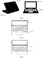
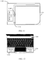
FIG. 1 is a schematic diagram of a basic structure of a notebook computer according to an embodiment of this application. As shown inFIG. 1 , surfaces of the notebook computer are a surface A, a surface B, a surface C, and a surface D from top to bottom. The surface A, the surface B, and components between the surface A and the surface B form a display screen. The surface C, the surface D, and components between the surface C and the surface D form a keyboard and a host. The display screen and the keyboard and the host may be connected by using a hinge (hinge). -
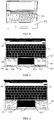
FIG. 2 is a schematic diagram of a layout of an LTE antenna in a notebook computer. As shown inFIG. 2 , anLTE antenna 210 is arranged at a top of a display screen of anotebook computer 200. This is currently a most common LTE antenna layout solution. In this solution, a cable length of the LTE antenna is relatively long, and is about 400 mm to 600 mm. Therefore, a cable loss (cable loss) is relatively large. In addition, this solution requires that a component of the surface A is nonmetallic, and a window needs to be opened in the surface B. In this way, clearance of the antenna reaches 13 mm to 20 mm. This is unfavorable to a metalization requirement and a full-screen requirement of a current notebook computer. In addition, as the notebook computer becomes ultra-thin, a thickness of the component of the surface A is usually less than 4 mm, and edge arcing processing is performed on the component of the surface A. Therefore, a conventional adjustable technical solution cannot be used to compress antenna space and implement a full-band antenna. -
FIG. 3 is a schematic diagram of another layout of an LTE antenna in a notebook computer. As shown inFIG. 3 , anLTE antenna 310 is arranged in a hinge cover at a bottom of a display screen of anotebook computer 300. In this solution, most LTE antennas are inverted F antennas (Inverted F Antenna, IFA). This solution requires that the hinge cover is nonmetallic, and a window is opened at a lower part of the surface B. This is unfavorable to a metalization requirement and a full-screen requirement of a current notebook computer. In addition, if a component of the surface C and/or a component of the surface D are/is metallic in this solution, low-frequency isolation between main and diversity antennas of the LTE antenna is very poor. In addition, mutual interference is generated between theLTE antenna 310 and a Wi-Fi antenna. -
FIG. 4 is a schematic diagram of still another layout of an LTE antenna in a notebook computer. As shown inFIG. 4 , anLTE antenna 410 is arranged between a surface C and a surface D of anotebook computer 400, and a position of theLTE antenna 410 corresponds to a hinge cover. In this solution, low-frequency isolation between main and diversity antennas of the LTE antenna is poor, and mutual interference is generated between theLTE antenna 410 and a Wi-Fi antenna. In addition, theLTE antenna 410 is adjacent to a host system, and a risk of interference between theLTE antenna 410 and the host system is relatively high. - To sum up, the notebook computer has the following restrictions on a mobile communication antenna due to its own features: Metallic bodies of the surface A, the surface C, and the surface D restrict a design of the mobile communication antenna. A full-screen trend and ultra-thin components of the surface A and the surface B make it impossible to deploy the mobile communication antenna in the surface A and the surface B. A large amount of manpower and material resources need to be invested for migrating an existing mobile communication antenna solution in a mobile phone and a tablet computer to the notebook computer.
- To resolve the foregoing problem, an embodiment of this application provides a mobile communication antenna solution that can meet requirements of a full-screen and a metallic body of the notebook computer. An antenna in this embodiment of this application may be applied to an electronic device such as a notebook computer, a portable computer, a mobile phone, or a tablet computer. However, this embodiment of this application is not limited thereto. The following mainly uses the notebook computer as an example for detailed description.
- It should be understood that an electronic device in the embodiments of this application may include but is not limited to a notebook computer, a portable computer, a mobile phone, a tablet computer, or the like. A slot antenna in the embodiments of this application may be disposed at a position such as a palm rest, a side edge, a side corner, a rear cover, an upper cover, or a lower cover of an electronic device such as a notebook computer, a portable computer, a mobile phone, or a tablet computer.
- An embodiment of this application provides an electronic device. A surface C of the electronic device includes a keyboard area used for inputting by using a keyboard, a touch area used for inputting by using a touchpad, and a palm rest. The palm rest is made of a metal material, and at least one radiating slot is disposed in the palm rest, to form a slot antenna.
- In the electronic device in this embodiment of this application, the slot antenna is arranged in the palm rest of the surface C of the electronic device, which has little impact on a layout of components in the electronic device. A manufacturing method of the slot antenna is simple, a size of the slot antenna is small, and the slot antenna can implement an ultra-wideband feature. The slot antenna can be applied to an electronic device with an ultra-thin and metallic body, and has strong portability. In addition, there is no need to add a redundant circuit to a radio frequency circuit.
- It should be understood that, in the embodiments of this application, the palm rest may be one or more areas on the surface C except the keyboard area and the touch area.
- It should be further understood that, in the embodiments of this application, the electronic device may further include a surface A used as a top cover, a surface B with a screen, and a surface D used as a bottom cover.
- From another perspective, an embodiment of this application provides a slot antenna. A metal radiator of the slot antenna is at least a part (for example, a part of the palm rest of the surface C) of a housing of the electronic device. The metal radiator may include a radiating slot, and the radiating slot has at least one pair of a grounding point and a feeding point.
-
FIG. 5 is a schematic structural diagram of anelectronic device 50 and a slot antenna according to an embodiment of this application. As shown inFIG. 5 , the electronic device to which the slot antenna is applied is anotebook computer 50. Akeyboard area 52, atouch area 54, and a palm rest (as shown inFIG. 5 , including aleft palm rest 56 and a right palm rest 58) are disposed on a surface C of thenotebook computer 50. A radiating slot is located in the palm rest of thenotebook computer 50. For example, a body of the slot antenna is a metal housing part including theleft palm rest 56 and theright palm rest 58 near thekeyboard area 52 of thenotebook computer 50. Theleft palm rest 56 and theright palm rest 58 include four radiating slots: a radiatingslot 510, aradiating slot 520, a radiating slot 530, and aradiating slot 540. Each radiating slot and a nearby metal body may be considered to form a slot antenna. Each radiating slot includes a pair of a feeding point and a grounding point. The radiatingslot 510 has agrounding point 512 and afeeding point 514. The radiatingslot 520 has agrounding point 522 and afeeding point 524. The radiating slot 530 has agrounding point 532 and afeeding point 534. The radiatingslot 540 has agrounding point 542 and afeeding point 544. - It should be understood that a quantity of radiating slots in the palm rest in
FIG. 5 is merely an example. In another embodiment, the palm rest may include only one radiating slot, for example, include only any one of theradiating slot 510, the radiatingslot 520, the radiating slot 530, and theradiating slot 540. In still another embodiment, the palm rest may include two radiating slots, for example, include theradiating slot 510 and theradiating slot 520, or include theradiating slot 510 and the radiating slot 530, or include theradiating slot 520 and theradiating slot 540, or the like. - It should be further understood that shapes of radiating slots in
FIG. 5 are merely examples. In different embodiments, radiating slots of different shapes may be selected based on a requirement of an operating frequency band of a product and/or a layout of metal components in the product, and the like. For example, the straight-line shaped radiating slot shown inFIG. 5 , and an L-shaped radiating slot shown inFIG. 6 . This is not enumerated one by one in this application. When there are a plurality of radiating slots in the palm rest, any two radiating slots may have a same shape, or may have different shapes. This is not limited in the embodiments of this application. - It should be further understood that sizes of radiating slots in
FIG. 5 are merely examples. In different embodiments, a length and a width of a radiating slot may be set based on a requirement of an operating frequency band of the product and/or a material shape of the product. When there are a plurality of radiating slots in the palm rest, any two radiating slots may have a same length and/or width, or may have different lengths and/or widths. This is not limited in the embodiments of this application. - It should be further understood that positions of the grounding point and the feeding point in each radiating slot in
FIG. 5 are merely examples. In different embodiments, a grounding point and a feeding point may be disposed at an appropriate position selected from a radiating slot based on a requirement of an operating frequency band of a product. When there are a plurality of radiating slots in the palm rest, relative positions of grounding points and feeding points in the radiating slots may be the same or may be different. This is not limited in the embodiments of this application. -
FIG. 6 is a schematic structural diagram of anelectronic device 60 and a slot antenna according to another embodiment of this application. Akeyboard area 62, atouch area 64, and a palm rest (as shown inFIG. 6 , including aleft palm rest 66 and a right palm rest 68) are disposed on a surface C of theelectronic device 60 shown inFIG. 6 . Radiating slots in theleft palm rest 66 and theright palm rest 68 are L-shaped slots. In this embodiment of this application, an L-shaped radiating slot may be disposed in only one palm rest, or an L-shaped radiating slot may be separately disposed in a left palm rest and a right palm rest, and one or more L-shaped radiating slots may be disposed in each palm rest. The L-shaped radiating slot is separately disposed in theleft palm rest 66 and theright palm rest 68 of theelectronic device 60 shown inFIG. 6 : an L-shapedradiating slot 610 and an L-shapedradiating slot 620. The L-shaped radiating slot is easily arranged in a housing of the electronic device, and a formed operating frequency band of the slot antenna is wide. - A first part of the L-shaped
radiating slot 610 has afirst feeding point 614 and afirst grounding point 612, thefirst grounding point 612 is closer to a first end (an end close to a touchpad) of the first part (a part close to and parallel to a long side of the keyboard area) than thefirst feeding point 614, and thefirst grounding point 612 is farther from a second end (an end close to an edge of the housing) of the first part than thefirst feeding point 614. A second part (a part parallel to and close to the touchpad) of the L-shapedradiating slot 610 has asecond feeding point 618 and asecond grounding point 616, thesecond grounding point 616 is closer to a third end (an end close to the keyboard area) of the second part than thesecond feeding point 618, thesecond grounding point 616 is farther from a fourth end (an end close to an edge of the housing) of the second part than thesecond feeding point 618, and the first end coincides with the third end. - A third part of the L-shaped
radiating slot 620 has athird feeding point 624 and athird grounding point 622, thethird grounding point 622 is closer to a fifth end (an end close to the touchpad) of the third part (a part close to and parallel to the long side of the keyboard area) than thethird feeding point 624, and thethird grounding point 622 is farther from a sixth end (an end close to the edge of the housing) of the third part than thethird feeding point 624. A fourth part (a part parallel to and close to the touchpad) of the L-shapedradiating slot 620 has afourth feeding point 628 and afourth grounding point 626, thefourth grounding point 626 is closer to a seventh end (an end close to the keyboard area) of the fourth part than thefourth feeding point 628, thefourth grounding point 626 is farther from an eighth end (an end close to the edge of the housing) of the fourth part than thefourth feeding point 628, and the fifth end coincides with the seventh end. - As shown in
FIG. 6 , the first part of the L-shapedradiating slot 610 is parallel and close to the long side of the keyboard area, and the second part of the L-shapedradiating slot 610 is perpendicular to the first part and parallel and close to a side of the touch area. Two parts of the L-shapedradiating slot 620 are also disposed similar to the L-shapedradiating slot 610. The L-shaped radiating slot is disposed in the palm rest in this possible implementation, and does not affect a layout of other components of the electronic device. This ensures performance of the slot antenna. - In another embodiment of this application, the L-shaped radiating slot may be disposed in the palm rest in a form shown in
FIG. 6 , or may be disposed in the palm rest in another form. For example, an included angle of the L-shaped radiating slot may be distributed near the other three corners or any position of the palm rest other than the palm rest inFIG. 6 . When the palm rest includes a plurality of L-shaped radiating slots, distribution of the L-shaped radiating slots in the palm rest may be symmetric or asymmetric. This is not limited in the embodiments of this application. - Optionally, the L-shaped radiating slot may implement a low-frequency function and a high-frequency function.
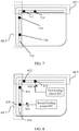
FIG. 7 is a schematic diagram of an L-shapedradiating slot 710 according to an embodiment of this application. As shown inFIG. 7 , a length of a first part of the L-shapedradiating slot 710 and a length of a second part of the L-shapedradiating slot 710 are greater than 50 millimeters. The first part of the L-shaped radiating slot and metal around the slot may form a firstsub-antenna ant 1, and a distance between afirst feeding point 714 on theant 1 and a second end of the first part is greater than 35 millimeters. In other words, a distance between afirst grounding point 712 and thefirst feeding point 714 on theant 1 is relatively small, and thefirst feeding point 714 is far away from an edge of a housing. Therefore, theant 1 may be considered as a low-frequency sub-antenna. The second part of the L-shaped radiating slot and metal around the slot may form a secondsub-antenna ant 2, and a distance between asecond feeding point 718 on theant 2 and a fourth end of the second part is greater than or equal to 10 millimeters and less than or equal to 30 millimeters. In other words, a distance between asecond grounding point 716 and thesecond feeding point 718 on theant 2 is relatively large, and thesecond feeding point 718 is close to the edge of the housing. Therefore, theant 2 may be considered as a high-frequency sub-antenna. It should be understood that the firstsub-antenna ant 1 and the secondsub-antenna ant 2 may be interchanged as a whole. It should be understood that, in another embodiment of this application, thefirst feeding point 714 and/or thesecond feeding point 718 may be disposed at a position other than the foregoing range, to adapt to various frequency band requirements. This is not limited in the embodiments of this application. - Optionally, in an embodiment provided in this application, a first feeding point may be connected to a first feeding circuit by using a first tunable capacitor.
FIG. 8 is a schematic diagram of an L-shapedradiating slot 810 according to another embodiment of this application. As shown inFIG. 8 , a firsttunable capacitor 822 may be connected in series between afirst feeding point 814 and afirst feeding circuit 820, and a capacitance value of the firsttunable capacitor 822 is tunable within a range from 0 to a specific value. In this way, an equivalent length between afirst grounding point 812 and thefirst feeding point 814 may be tuned by using the firsttunable capacitor 822, to implement that a frequency band of a firstsub-antenna ant 1 is tunable. - Optionally, in an embodiment provided in this application, a second feeding point may be connected to a second feeding circuit by using a second adjustable capacitor component. As shown in
FIG. 8 , a secondtunable capacitor 832 may be connected in series between asecond feeding point 818 and asecond feeding circuit 830, and a capacitance value of the secondtunable capacitor 832 is tunable within a range from 0 to a specific value. In this way, an equivalent length between asecond grounding point 816 and thesecond feeding point 818 may be tuned by using the secondtunable capacitor 832, to implement that a frequency band of a secondsub-antenna ant 2 is tunable. It should be understood that the firsttunable capacitor 822 is connected in series between thefirst feeding point 814 and thefirst feeding circuit 820, and the secondtunable capacitor 832 is connected in series between thesecond feeding point 818 and thesecond feeding circuit 830 are both optional. This is not limited in the embodiments of this application. - According to the foregoing similar principles, this application may provide a full-band slot antenna.
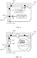
FIG. 9 is a schematic diagram of an L-shapedradiating slot 910 according to still another embodiment of this application. Optionally, in an embodiment provided in this application, afirst feeding point 914 may be disposed at a position that is relatively close to an edge of a housing (for example, a distance between thefirst feeding point 914 and the edge of the housing is greater than or equal to 10 millimeters and less than or equal to 15 millimeters), to implement a high-frequency band of a firstsub-antenna ant 1. A firsttunable capacitor 922 may be connected in series between thefirst feeding point 914 and afirst feeding circuit 920, or a first fixed capacitor may be connected in series between thefirst feeding point 914 and thefirst feeding circuit 920 under control of a switch. An equivalent length between afirst grounding point 912 and thefirst feeding point 914 is tuned by using the firsttunable capacitor 922 or the first fixed capacitor, to implement a low-frequency band of the firstsub-antenna ant 1. - Optionally, in an embodiment provided in this application, a
second feeding point 918 may be disposed at a position that is relatively close to an edge of a housing (for example, a distance between thesecond feeding point 918 and the edge of the housing is greater than or equal to 10 millimeters and less than or equal to 15 millimeters), to implement a high-frequency band of a secondsub-antenna ant 2. A secondtunable capacitor 932 may be connected in series between thesecond feeding point 918 and asecond feeding circuit 930, or a second fixed capacitor may be connected in series between thesecond feeding point 918 and thesecond feeding circuit 930 under control of a switch. An equivalent length between asecond grounding point 916 and thesecond feeding point 918 is tuned by using the secondtunable capacitor 932 or the second fixed capacitor, to implement a low-frequency band of the secondsub-antenna ant 2. - It should be understood that the
ant 1 may be a full-band antenna, and theant 2 may also be a full-band antenna. An L-shaped radiating slot can implement a 2x2 full-band antenna. Two L-shaped radiating slots can implement a 4x4 full-band antenna. - A low-frequency band state tuned by a capacitor connected in series at a feeding point usually has a relatively small bandwidth. This application provides another embodiment, which may cover a full-band and a low-band.
FIG. 10 is a schematic diagram of an L-shapedradiating slot 1010 according to yet another embodiment of this application. Optionally, in an embodiment provided in this application, as shown inFIG. 10 , a first part of the L-shapedradiating slot 1010, afirst grounding point 1012 on the first part, and afirst feeding point 1014 on the first part may form a firstsub-antenna ant 1. There is a first frequency band adjustment point between the first grounding point and the first feeding point, a first selection component is disposed at the first frequency band adjustment point, and the first selection component is configured to select inductance components with different inductance values to connect to metal on two sides of a slot at the first frequency band adjustment point. Specifically, an appropriate position between thefirst grounding point 1012 and thefirst feeding point 1014 may be selected to connect to the first selection component (for example, afirst switch 1020 inFIG. 10 ) that is across the slot. By using thefirst switch 1020, one of different inductors L1, L2, L3, ... may be selected, to implement wide-band coverage of a low-frequency band of the firstsub-antenna ant 1. It should be understood that, when the L1 is connected, other inductors (L2, L3...) are in a non-connected state. - A second part of the L-shaped
radiating slot 1010, asecond grounding point 1016 on the second part, and asecond feeding point 1018 on the second part may form a secondsub-antenna ant 2. There is a second frequency band adjustment point between the second grounding point and the second feeding point, a second selection component is disposed at the second frequency band adjustment point, and the second selection component is configured to select inductance components with different inductance values to connect to metal on two sides of a slot at the second frequency band adjustment point. Specifically, an appropriate position between thesecond grounding point 1016 and thesecond feeding point 1018 may be selected to connect to the second selection component (for example, a second switch 1030) that is across the slot. Similarly, one inductor may be selected from different inductors by using thesecond switch 1030, to implement wide-band coverage of a low-frequency band of the secondsub-antenna ant 2. Details are not described herein again. - In the electronic device in the embodiments of this application, the slot antenna may be disposed in the surface C, and the L-shaped radiating slot is disposed at a palm rest position, to implement full-band antenna coverage, and resolve problems of a full-screen, a metallic body, and isolation between multi-antenna systems.
- In an embodiment of this application, the electronic device may include a specific absorption rate (Specific Absorption Rate, SAR) sensor (sensor). The SAR sensor includes a sensor body and a sensor circuit. A working principle of the SAR sensor requires that the sensor body cannot be grounded and the sensor circuit works in an approximate direct-current state.
FIG. 11 is a schematic diagram of a partial structure of anelectronic device 1100 according to an embodiment of this application. In this embodiment of this application, theelectronic device 1100 includes an antenna and an SAR sensor.FIG. 11 shows a metal radiator of the antenna and an L-shapedradiating slot 1110 in the metal radiator. At least a part of a metal body of a palm rest may be used as a sensor body of the SAR sensor (also a metal radiator of a slot antenna). For example, apart 1120 in a dashed-line box shown inFIG. 11 may be used as the sensor body of the SAR sensor. Asensor circuit 1130 of the SAR sensor may be connected to asensor body 1120 by connecting in series aninductor 1140 with a relatively large inductance value (a feature of theinductor 1140 is that a direct-current is turned on and a high-frequency is turned off). An access point at which thesensor circuit 1130 is connected to thesensor body 1120 is not limited, and thesensor circuit 1130 may be connected to thesensor body 1120 at any position of the L-shapedradiating slot 1110. For ease of design, in this embodiment of this application, the sensor body of the SAR sensor may be connected to the sensor circuit by using at least one of a first feeding point, a first grounding point, a second feeding point, and a second grounding point (not shown inFIG. 11 ). To ensure that the sensor body is not grounded, in this embodiment of this application, the first grounding point of the L-shaped radiating slot is grounded by using a first capacitor, and the second grounding point is grounded by using a second capacitor. According to the design of this embodiment of this application, the SAR sensor and the antenna do not affect each other, and can work normally and efficiently. - Optionally, in an embodiment of this application, an area that is on a surface D of the electronic device and that is opposite to a radiating slot has a window, or the area that is on the surface D of the electronic device and that is opposite to the radiating slot is nonmetallic. This can ensure performance of the slot antenna.
- Optionally, a metal component may be arranged in a part covered by a palm rest of the electronic device in this embodiment of this application, and a flat cable of the metal component is connected to a host system by using space between the first grounding point and the second grounding point.
- Optionally, in the electronic device in this embodiment of this application, the palm rest includes a left palm rest and a right palm rest, and a slot antenna is separately formed in the left palm rest and the right palm rest. The electronic device further includes a sensor, and the sensor is configured to detect whether a palm of a user approaches the left palm rest or the right palm rest. When the palm of the user approaches only one of the left palm rest and the right palm rest, the electronic device disables operating of a slot antenna in a palm rest that the palm of the user approaches, and keeps operating of a slot antenna in a palm rest that the palm of the user does not approach.
-
FIG. 12 is a schematic structural diagram of anelectronic device 1200 according to another embodiment of this application. As shown inFIG. 12 , in theelectronic device 1200 in this embodiment of this application, a palm rest includes aleft palm rest 1210 and aright palm rest 1220, and a slot antenna is separately formed in theleft palm rest 1210 and theright palm rest 1220. Theelectronic device 1200 further includes asensor 1230 and asensor 1240, thesensor 1230 is configured to detect whether a palm of a user approaches theleft palm rest 1210, and thesensor 1240 is configured to detect whether the palm of the user approaches theright palm rest 1220. When it is detected that the palm of the user approaches only one of theleft palm rest 1210 and theright palm rest 1220, theelectronic device 1200 disables operating of a slot antenna in a palm rest that the palm of the user approaches, and keeps operating of a slot antenna in a palm rest that the palm of the user does not approach. This reduces power consumption of the electronic device. - It should be understood that division of a circuit, a sub-circuit, and a sub-unit in the embodiments of this application is merely an example. A person of ordinary skill in the art may be aware that circuits, sub-circuits, and sub-units in the examples described in the embodiments disclosed in this specification can be further divided or combined.
- All or some of the foregoing embodiments may be implemented by using software, hardware, firmware, or any combination thereof. When software is used to implement the embodiments, the embodiments may be implemented completely or partially in a form of a computer program product. The computer program product includes one or more computer instructions. When the computer instructions are loaded and executed on the computer, the procedure or functions according to the embodiments of this application are all or partially generated. The computer may be a general-purpose computer, a dedicated computer, a computer network, or other programmable apparatuses. The computer instructions may be stored in a computer-readable storage medium or may be transmitted from a computer-readable storage medium to another computer-readable storage medium. For example, the computer instructions may be transmitted from a website, computer, server, or data center to another website, computer, server, or data center in a wired (for example, a coaxial cable, an optical fiber, or a digital subscriber line (Digital Subscriber Line, DSL)) or wireless (for example, infrared, radio, and microwave, or the like) manner. The computer storage medium may be any usable medium accessible by a computer, or a data storage device, such as a server or a data center, integrating one or more usable media. The usable medium may be a magnetic medium (for example, a floppy disk, a hard disk, or a magnetic tape), an optical medium (for example, a high-density digital video disc (Digital Video Disc, DVD), a semiconductor medium (for example, a solid state drive (Solid State Disk, SSD)), or the like.
- It should be understood that "an embodiment" or "an embodiment" mentioned in the whole specification does not mean that particular features, structures, or characteristics related to the embodiment are included in at least one embodiment of this application. Therefore, "in an embodiment" or "in an embodiment" appearing throughout the specification does not refer to a same embodiment. In addition, these particular features, structures, or characteristics may be combined in one or more embodiments by using any appropriate manner.
- It should be understood that sequence numbers of the foregoing processes do not mean execution sequences in various embodiments of this application. The execution sequences of the processes should be determined according to functions and internal logic of the processes, and should not be construed as any limitation on the implementation processes of the embodiments of this application.
- It should be understood that in the embodiments of this application, "B corresponding to A" indicates that B is associated with A, and B may be determined based on A. However, it should further be understood that determining A based on B does not mean that B is determined based on A only. In other words, B may also be determined based on A and/or other information.
- The term "and/or" in this specification describes only an association relationship for describing associated objects and represents that three relationships may exist. For example, A and/or B may represent the following three cases: Only A exists, both A and B exist, and only B exists. In addition, the character "/" in this specification generally indicates an "or" relationship between the associated objects.
- A person of ordinary skill in the art may be aware that, in combination with the examples described in the embodiments disclosed in this specification, units and algorithm steps may be implemented by electronic hardware or a combination of computer software and electronic hardware. Whether the functions are performed by hardware or software depends on particular applications and design constraint conditions of the technical solutions. A person skilled in the art may use different methods to implement the described functions for each particular application, but it should not be considered that the implementation goes beyond the scope of this application.
- It may be clearly understood by a person skilled in the art that, for the purpose of convenient and brief description, for a detailed working process of the foregoing system, apparatus, and unit, refer to a corresponding process in the foregoing method embodiments. Details are not described herein again.
- In the several embodiments provided in this application, it should be understood that the disclosed system, apparatus, and method may be implemented in other manners. For example, the described apparatus embodiment is merely an example. For example, the unit division is merely logical function division and may be other division in actual implementation. For example, a plurality of units or components may be combined or integrated into another system, or some features may be ignored or not performed. In addition, the displayed or discussed mutual couplings or direct couplings or communication connections may be implemented by using some interfaces. The indirect couplings or communication connections between the apparatuses or units may be implemented in electronic, mechanical, or other forms.
- The units described as separate parts may or may not be physically separate, and parts displayed as units may or may not be physical units, may be located in one position, or may be distributed on a plurality of network units. Some or all of the units may be selected based on actual requirements to achieve the objectives of the solutions of the embodiments.
- In addition, functional units in the embodiments of this application may be integrated into one processing unit, or each of the units may exist alone physically, or two or more units are integrated into one unit.
- The foregoing descriptions are merely specific implementations of this application, but are not intended to limit the protection scope of this application. Any variation or replacement readily figured out by a person skilled in the art within the technical scope disclosed in this application shall fall within the protection scope of this application. Therefore, the protection scope of this application shall be subject to the protection scope of the claims.
Claims (19)
- An electronic device, wherein a surface C comprises a keyboard area used for inputting by using a keyboard, a touch area used for inputting by using a touchpad, and a palm rest, the palm rest is made of a metal material, and at least one radiating slot is disposed in the palm rest, to form a slot antenna.
- The electronic device according to claim 1, wherein the at least one radiating slot comprises an L-shaped radiating slot.
- The electronic device according to claim 2, wherein a first part of the L-shaped radiating slot has a first feeding point and a first grounding point, the first grounding point is closer to a first end of the first part than the first feeding point, and the first grounding point is farther from a second end of the first part than the first feeding point; and
a second part of the L-shaped radiating slot has a second feeding point and a second grounding point, the second grounding point is closer to a third end of the second part than the second feeding point, the second grounding point is farther from a fourth end of the second part than the second feeding point, and the first end coincides with the third end. - The electronic device according to claim 3, wherein the first part is parallel to and close to a long side of the keyboard area, and the second part is perpendicular to the first part and parallel to and close to a side of the touch area.
- The electronic device according to claim 3 or 4, wherein a length of the first part and a length of the second part are greater than 50 millimeters.
- The electronic device according to any one of claims 3 to 5, wherein a distance between the first feeding point and the second end is greater than 35 millimeters.
- The electronic device according to any one of claims 3 to 6, wherein a distance between the second feeding point and the fourth end is greater than or equal to 10 millimeters and less than or equal to 30 millimeters.
- The electronic device according to any one of claims 3 to 6, wherein the first grounding point is grounded by using a first capacitor, the second grounding point is grounded by using a second capacitor, the electronic device further comprises a specific absorption rate, SAR sensor, and at least a part of a metal body of the palm rest is used as a sensor body of the SAR sensor.
- The electronic device according to claim 8, wherein the sensor body of the SAR sensor is connected to a sensor circuit by using at least one of the first feeding point, the first grounding point, the second feeding point, and the second grounding point.
- The electronic device according to any one of claims 3 to 9, wherein a metal component is arranged in a part covered by the palm rest of the electronic device, and a flat cable of the metal component is connected to a host system by using space between the first grounding point and the second grounding point.
- The electronic device according to any one of claims 3 to 10, wherein the first feeding point is connected to a first feeding circuit by using a first tunable capacitor.
- The electronic device according to any one of claims 3 to 11, wherein the second feeding point is connected to a second feeding circuit by using a second tunable capacitor.
- The electronic device according to any one of claims 3 to 12, wherein there is a first frequency band adjustment point between the first grounding point and the first feeding point, a first selection component is disposed at the first frequency band adjustment point, and the first selection component is configured to select inductance components with different inductance values to connect to metal on two sides of a slot at the first frequency band adjustment point.
- The electronic device according to any one of claims 3 to 13, wherein there is a second frequency band adjustment point between the second grounding point and the second feeding point, a second selection component is disposed at the second frequency band adjustment point, and the second selection component is configured to select inductance components with different inductance values to connect to metal on two sides of a slot at the second frequency band adjustment point.
- The electronic device according to any one of claims 1 to 14, wherein an area that is on a surface D of the electronic device and that is opposite to the radiating slot has a window, or the area that is on the surface D of the electronic device and that is opposite to the radiating slot is nonmetallic.
- The electronic device according to any one of claims 1 to 15, wherein the palm rest is one or more areas on the surface C except the keyboard area and the touch area.
- The electronic device according to any one of claims 1 to 16, wherein the palm rest comprises a left palm rest and a right palm rest, the slot antenna is separately formed in the left palm rest and the right palm rest, the electronic device further comprises a sensor, the sensor is configured to detect whether a palm of a user approaches the left palm rest or the right palm rest, and when the palm of the user approaches only one of the left palm rest and the right palm rest, the electronic device disables operating of a slot antenna in a palm rest that the palm of the user approaches, and keeps operating of a slot antenna in a palm rest that the palm of the user does not approach.
- The electronic device according to any one of claims 1 to 17, wherein the electronic device further comprises a surface A used as a top cover, a surface B with a screen, and a surface D used as a bottom cover.
- The electronic device according to any one of claims 1 to 18, wherein the slot antenna is a mobile communication antenna.
Applications Claiming Priority (1)
| Application Number | Priority Date | Filing Date | Title |
|---|---|---|---|
| PCT/CN2018/085036 WO2019205120A1 (en) | 2018-04-28 | 2018-04-28 | Electronic device having slot antenna |
Publications (4)
| Publication Number | Publication Date |
|---|---|
| EP3780263A1 true EP3780263A1 (en) | 2021-02-17 |
| EP3780263A4 EP3780263A4 (en) | 2021-03-24 |
| EP3780263B1 EP3780263B1 (en) | 2022-12-21 |
| EP3780263B8 EP3780263B8 (en) | 2023-02-15 |
Family
ID=68294357
Family Applications (1)
| Application Number | Title | Priority Date | Filing Date |
|---|---|---|---|
| EP18916987.3A Active EP3780263B8 (en) | 2018-04-28 | 2018-04-28 | Electronic device having slot antenna |
Country Status (4)
| Country | Link |
|---|---|
| US (1) | US11575193B2 (en) |
| EP (1) | EP3780263B8 (en) |
| CN (1) | CN110892579B (en) |
| WO (1) | WO2019205120A1 (en) |
Families Citing this family (3)
| Publication number | Priority date | Publication date | Assignee | Title |
|---|---|---|---|---|
| KR102503483B1 (en) * | 2018-08-16 | 2023-02-27 | 삼성전자주식회사 | Antenna switch changing method based on data processing speed estimation and electronic device thereof |
| CN113555692B (en) * | 2020-04-23 | 2023-02-03 | 华为技术有限公司 | Electronic equipment |
| WO2023163451A1 (en) * | 2022-02-24 | 2023-08-31 | 삼성전자주식회사 | Antenna and electronic apparatus including same |
Family Cites Families (21)
| Publication number | Priority date | Publication date | Assignee | Title |
|---|---|---|---|---|
| JP2003152430A (en) * | 2001-11-09 | 2003-05-23 | Hitachi Cable Ltd | Two frequency planar antenna and electric apparatus comprising it |
| US6864848B2 (en) * | 2001-12-27 | 2005-03-08 | Hrl Laboratories, Llc | RF MEMs-tuned slot antenna and a method of making same |
| JP2003234615A (en) * | 2002-02-06 | 2003-08-22 | Nec Corp | Slot antenna and radio lan card |
| US20050146475A1 (en) * | 2003-12-31 | 2005-07-07 | Bettner Allen W. | Slot antenna configuration |
| JP5132370B2 (en) | 2007-03-30 | 2013-01-30 | パナソニック株式会社 | MIMO communication equipment |
| US8077096B2 (en) * | 2008-04-10 | 2011-12-13 | Apple Inc. | Slot antennas for electronic devices |
| JP5102170B2 (en) * | 2008-10-09 | 2012-12-19 | 富士通株式会社 | Electronics |
| US9058152B2 (en) | 2009-08-24 | 2015-06-16 | Ralink Technology Corporation | Wireless communication module, portable device using the same and method for manufacturing the same |
| US9799943B2 (en) | 2010-11-30 | 2017-10-24 | Intel Corporation | Cable antenna apparatus and system |
| CN202352829U (en) | 2011-12-15 | 2012-07-25 | 上海安费诺永亿通讯电子有限公司 | Wideband-tunable antenna applied to mobile terminal |
| TWI493783B (en) | 2012-06-22 | 2015-07-21 | Acer Inc | Communication device |
| TWI528640B (en) | 2012-11-20 | 2016-04-01 | 啟碁科技股份有限公司 | Wideband antenna and wireless communication device |
| CN103840251B (en) | 2012-11-22 | 2016-08-03 | 启碁科技股份有限公司 | Broad-band antenna and radio communication device |
| KR101944340B1 (en) | 2012-12-28 | 2019-01-31 | 엘지디스플레이 주식회사 | Slot antenna and information terminal apparatus using the same |
| GB2533339A (en) | 2014-12-17 | 2016-06-22 | Vertu Corp Ltd | Multiband slot antenna system and apparatus |
| CN204991944U (en) * | 2015-10-15 | 2016-01-20 | 合肥联宝信息技术有限公司 | Slot antenna and be equipped with this slot antenna's electronic equipment |
| CN105680153B (en) * | 2016-03-18 | 2019-02-15 | 努比亚技术有限公司 | A kind of antenna and terminal |
| JP2017227976A (en) * | 2016-06-20 | 2017-12-28 | レノボ・シンガポール・プライベート・リミテッド | Device for implementing division display of screen, method therefor, and program product therefor |
| CN106099327B (en) * | 2016-06-28 | 2019-07-30 | 惠州硕贝德无线科技股份有限公司 | Near field antenna device and its equipment |
| US10511083B2 (en) * | 2016-09-22 | 2019-12-17 | Apple Inc. | Antennas having symmetrical switching architecture |
| CN107548145A (en) * | 2017-06-27 | 2018-01-05 | 西安易朴通讯技术有限公司 | Antenna assembly, mobile terminal and antenna adjustment method |
-
2018
- 2018-04-28 WO PCT/CN2018/085036 patent/WO2019205120A1/en unknown
- 2018-04-28 US US17/050,559 patent/US11575193B2/en active Active
- 2018-04-28 EP EP18916987.3A patent/EP3780263B8/en active Active
- 2018-04-28 CN CN201880046246.9A patent/CN110892579B/en active Active
Also Published As
| Publication number | Publication date |
|---|---|
| WO2019205120A1 (en) | 2019-10-31 |
| CN110892579B (en) | 2021-08-03 |
| EP3780263B8 (en) | 2023-02-15 |
| US20210242567A1 (en) | 2021-08-05 |
| CN110892579A (en) | 2020-03-17 |
| EP3780263A4 (en) | 2021-03-24 |
| US11575193B2 (en) | 2023-02-07 |
| EP3780263B1 (en) | 2022-12-21 |
Similar Documents
| Publication | Publication Date | Title |
|---|---|---|
| EP3644441B1 (en) | Antenna circuit and mobile terminal | |
| EP2405533B1 (en) | Multiband antenna and method for an antenna to be capable of multiband operation | |
| US9698483B2 (en) | Aerial device and method for setting aerial device | |
| US11575193B2 (en) | Electronic device with slot antenna | |
| US20140218250A1 (en) | Case and electronic apparatus | |
| TWI448008B (en) | Handheld device and planar antenna thereof | |
| US10852782B2 (en) | Information handling system antenna isolation with integrated cooling fan | |
| US9124000B2 (en) | Current breaker and wireless communication device having the same | |
| EP2978198B1 (en) | Mobile wireless communications device with improved broadband antenna impedance matching | |
| WO2018176279A1 (en) | Antenna, and terminal apparatus | |
| WO2017073020A1 (en) | Electronic device | |
| CN110048230B (en) | Compact antenna and mobile terminal | |
| CN203481380U (en) | Antenna used for mobile terminal, mobile terminal shell and the mobile terminal | |
| US7388545B2 (en) | Shielding device | |
| US10522898B2 (en) | Integration of millimeter wave antennas in reduced form factor platforms | |
| US9048532B2 (en) | Multi-band antenna | |
| US11522295B2 (en) | Antenna structure | |
| CN111063985B (en) | Electronic device | |
| EP3968464A1 (en) | Electronic device | |
| US20130335909A1 (en) | Memory apparatus and electronic apparatus | |
| KR20140100384A (en) | Case and electronic apparatus | |
| CN105720348A (en) | Electronic device and mobile terminal provided with same | |
| US10283838B2 (en) | Multi-mode mobile device and radiation enhancing device | |
| Chen et al. | Reconfigurable narrow open-slot LTE MIMO antennas for metal-rimmed smartphone applications | |
| US11024966B2 (en) | Antenna and terminal device having same |
Legal Events
| Date | Code | Title | Description |
|---|---|---|---|
| STAA | Information on the status of an ep patent application or granted ep patent |
Free format text: STATUS: THE INTERNATIONAL PUBLICATION HAS BEEN MADE |
|
| PUAI | Public reference made under article 153(3) epc to a published international application that has entered the european phase |
Free format text: ORIGINAL CODE: 0009012 |
|
| STAA | Information on the status of an ep patent application or granted ep patent |
Free format text: STATUS: REQUEST FOR EXAMINATION WAS MADE |
|
| 17P | Request for examination filed |
Effective date: 20201027 |
|
| AK | Designated contracting states |
Kind code of ref document: A1 Designated state(s): AL AT BE BG CH CY CZ DE DK EE ES FI FR GB GR HR HU IE IS IT LI LT LU LV MC MK MT NL NO PL PT RO RS SE SI SK SM TR |
|
| AX | Request for extension of the european patent |
Extension state: BA ME |
|
| A4 | Supplementary search report drawn up and despatched |
Effective date: 20210224 |
|
| RIC1 | Information provided on ipc code assigned before grant |
Ipc: H01Q 1/22 20060101AFI20210218BHEP Ipc: H01Q 13/10 20060101ALI20210218BHEP Ipc: H01Q 13/16 20060101ALI20210218BHEP |
|
| DAV | Request for validation of the european patent (deleted) | ||
| DAX | Request for extension of the european patent (deleted) | ||
| GRAP | Despatch of communication of intention to grant a patent |
Free format text: ORIGINAL CODE: EPIDOSNIGR1 |
|
| STAA | Information on the status of an ep patent application or granted ep patent |
Free format text: STATUS: GRANT OF PATENT IS INTENDED |
|
| INTG | Intention to grant announced |
Effective date: 20220914 |
|
| GRAS | Grant fee paid |
Free format text: ORIGINAL CODE: EPIDOSNIGR3 |
|
| GRAA | (expected) grant |
Free format text: ORIGINAL CODE: 0009210 |
|
| STAA | Information on the status of an ep patent application or granted ep patent |
Free format text: STATUS: THE PATENT HAS BEEN GRANTED |
|
| AK | Designated contracting states |
Kind code of ref document: B1 Designated state(s): AL AT BE BG CH CY CZ DE DK EE ES FI FR GB GR HR HU IE IS IT LI LT LU LV MC MK MT NL NO PL PT RO RS SE SI SK SM TR |
|
| REG | Reference to a national code |
Ref country code: GB Ref legal event code: FG4D |
|
| REG | Reference to a national code |
Ref country code: CH Ref legal event code: EP |
|
| RAP4 | Party data changed (patent owner data changed or rights of a patent transferred) |
Owner name: HUAWEI TECHNOLOGIES CO., LTD. |
|
| REG | Reference to a national code |
Ref country code: DE Ref legal event code: R096 Ref document number: 602018044612 Country of ref document: DE |
|
| REG | Reference to a national code |
Ref country code: AT Ref legal event code: REF Ref document number: 1539600 Country of ref document: AT Kind code of ref document: T Effective date: 20230115 |
|
| REG | Reference to a national code |
Ref country code: IE Ref legal event code: FG4D |
|
| REG | Reference to a national code |
Ref country code: CH Ref legal event code: PK Free format text: BERICHTIGUNG B8 |
|
| REG | Reference to a national code |
Ref country code: LT Ref legal event code: MG9D |
|
| REG | Reference to a national code |
Ref country code: NL Ref legal event code: MP Effective date: 20221221 |
|
| PG25 | Lapsed in a contracting state [announced via postgrant information from national office to epo] |
Ref country code: SE Free format text: LAPSE BECAUSE OF FAILURE TO SUBMIT A TRANSLATION OF THE DESCRIPTION OR TO PAY THE FEE WITHIN THE PRESCRIBED TIME-LIMIT Effective date: 20221221 Ref country code: NO Free format text: LAPSE BECAUSE OF FAILURE TO SUBMIT A TRANSLATION OF THE DESCRIPTION OR TO PAY THE FEE WITHIN THE PRESCRIBED TIME-LIMIT Effective date: 20230321 Ref country code: LT Free format text: LAPSE BECAUSE OF FAILURE TO SUBMIT A TRANSLATION OF THE DESCRIPTION OR TO PAY THE FEE WITHIN THE PRESCRIBED TIME-LIMIT Effective date: 20221221 Ref country code: FI Free format text: LAPSE BECAUSE OF FAILURE TO SUBMIT A TRANSLATION OF THE DESCRIPTION OR TO PAY THE FEE WITHIN THE PRESCRIBED TIME-LIMIT Effective date: 20221221 |
|
| REG | Reference to a national code |
Ref country code: AT Ref legal event code: MK05 Ref document number: 1539600 Country of ref document: AT Kind code of ref document: T Effective date: 20221221 |
|
| PG25 | Lapsed in a contracting state [announced via postgrant information from national office to epo] |
Ref country code: RS Free format text: LAPSE BECAUSE OF FAILURE TO SUBMIT A TRANSLATION OF THE DESCRIPTION OR TO PAY THE FEE WITHIN THE PRESCRIBED TIME-LIMIT Effective date: 20221221 Ref country code: LV Free format text: LAPSE BECAUSE OF FAILURE TO SUBMIT A TRANSLATION OF THE DESCRIPTION OR TO PAY THE FEE WITHIN THE PRESCRIBED TIME-LIMIT Effective date: 20221221 Ref country code: HR Free format text: LAPSE BECAUSE OF FAILURE TO SUBMIT A TRANSLATION OF THE DESCRIPTION OR TO PAY THE FEE WITHIN THE PRESCRIBED TIME-LIMIT Effective date: 20221221 Ref country code: GR Free format text: LAPSE BECAUSE OF FAILURE TO SUBMIT A TRANSLATION OF THE DESCRIPTION OR TO PAY THE FEE WITHIN THE PRESCRIBED TIME-LIMIT Effective date: 20230322 |
|
| PGFP | Annual fee paid to national office [announced via postgrant information from national office to epo] |
Ref country code: GB Payment date: 20230309 Year of fee payment: 6 |
|
| PG25 | Lapsed in a contracting state [announced via postgrant information from national office to epo] |
Ref country code: NL Free format text: LAPSE BECAUSE OF FAILURE TO SUBMIT A TRANSLATION OF THE DESCRIPTION OR TO PAY THE FEE WITHIN THE PRESCRIBED TIME-LIMIT Effective date: 20221221 |
|
| PG25 | Lapsed in a contracting state [announced via postgrant information from national office to epo] |
Ref country code: SM Free format text: LAPSE BECAUSE OF FAILURE TO SUBMIT A TRANSLATION OF THE DESCRIPTION OR TO PAY THE FEE WITHIN THE PRESCRIBED TIME-LIMIT Effective date: 20221221 Ref country code: RO Free format text: LAPSE BECAUSE OF FAILURE TO SUBMIT A TRANSLATION OF THE DESCRIPTION OR TO PAY THE FEE WITHIN THE PRESCRIBED TIME-LIMIT Effective date: 20221221 Ref country code: PT Free format text: LAPSE BECAUSE OF FAILURE TO SUBMIT A TRANSLATION OF THE DESCRIPTION OR TO PAY THE FEE WITHIN THE PRESCRIBED TIME-LIMIT Effective date: 20230421 Ref country code: ES Free format text: LAPSE BECAUSE OF FAILURE TO SUBMIT A TRANSLATION OF THE DESCRIPTION OR TO PAY THE FEE WITHIN THE PRESCRIBED TIME-LIMIT Effective date: 20221221 Ref country code: EE Free format text: LAPSE BECAUSE OF FAILURE TO SUBMIT A TRANSLATION OF THE DESCRIPTION OR TO PAY THE FEE WITHIN THE PRESCRIBED TIME-LIMIT Effective date: 20221221 Ref country code: CZ Free format text: LAPSE BECAUSE OF FAILURE TO SUBMIT A TRANSLATION OF THE DESCRIPTION OR TO PAY THE FEE WITHIN THE PRESCRIBED TIME-LIMIT Effective date: 20221221 Ref country code: AT Free format text: LAPSE BECAUSE OF FAILURE TO SUBMIT A TRANSLATION OF THE DESCRIPTION OR TO PAY THE FEE WITHIN THE PRESCRIBED TIME-LIMIT Effective date: 20221221 |
|
| PGFP | Annual fee paid to national office [announced via postgrant information from national office to epo] |
Ref country code: DE Payment date: 20230307 Year of fee payment: 6 |
|
| PG25 | Lapsed in a contracting state [announced via postgrant information from national office to epo] |
Ref country code: SK Free format text: LAPSE BECAUSE OF FAILURE TO SUBMIT A TRANSLATION OF THE DESCRIPTION OR TO PAY THE FEE WITHIN THE PRESCRIBED TIME-LIMIT Effective date: 20221221 Ref country code: PL Free format text: LAPSE BECAUSE OF FAILURE TO SUBMIT A TRANSLATION OF THE DESCRIPTION OR TO PAY THE FEE WITHIN THE PRESCRIBED TIME-LIMIT Effective date: 20221221 Ref country code: IS Free format text: LAPSE BECAUSE OF FAILURE TO SUBMIT A TRANSLATION OF THE DESCRIPTION OR TO PAY THE FEE WITHIN THE PRESCRIBED TIME-LIMIT Effective date: 20230421 Ref country code: AL Free format text: LAPSE BECAUSE OF FAILURE TO SUBMIT A TRANSLATION OF THE DESCRIPTION OR TO PAY THE FEE WITHIN THE PRESCRIBED TIME-LIMIT Effective date: 20221221 |
|
| REG | Reference to a national code |
Ref country code: DE Ref legal event code: R097 Ref document number: 602018044612 Country of ref document: DE |
|
| PLBE | No opposition filed within time limit |
Free format text: ORIGINAL CODE: 0009261 |
|
| STAA | Information on the status of an ep patent application or granted ep patent |
Free format text: STATUS: NO OPPOSITION FILED WITHIN TIME LIMIT |
|
| PG25 | Lapsed in a contracting state [announced via postgrant information from national office to epo] |
Ref country code: DK Free format text: LAPSE BECAUSE OF FAILURE TO SUBMIT A TRANSLATION OF THE DESCRIPTION OR TO PAY THE FEE WITHIN THE PRESCRIBED TIME-LIMIT Effective date: 20221221 |
|
| 26N | No opposition filed |
Effective date: 20230922 |
|
| REG | Reference to a national code |
Ref country code: CH Ref legal event code: PL |
|
| PG25 | Lapsed in a contracting state [announced via postgrant information from national office to epo] |
Ref country code: LU Free format text: LAPSE BECAUSE OF NON-PAYMENT OF DUE FEES Effective date: 20230428 |
|
| REG | Reference to a national code |
Ref country code: BE Ref legal event code: MM Effective date: 20230430 |
|
| PG25 | Lapsed in a contracting state [announced via postgrant information from national office to epo] |
Ref country code: MC Free format text: LAPSE BECAUSE OF FAILURE TO SUBMIT A TRANSLATION OF THE DESCRIPTION OR TO PAY THE FEE WITHIN THE PRESCRIBED TIME-LIMIT Effective date: 20221221 |
|
| PG25 | Lapsed in a contracting state [announced via postgrant information from national office to epo] |
Ref country code: SI Free format text: LAPSE BECAUSE OF FAILURE TO SUBMIT A TRANSLATION OF THE DESCRIPTION OR TO PAY THE FEE WITHIN THE PRESCRIBED TIME-LIMIT Effective date: 20221221 Ref country code: MC Free format text: LAPSE BECAUSE OF FAILURE TO SUBMIT A TRANSLATION OF THE DESCRIPTION OR TO PAY THE FEE WITHIN THE PRESCRIBED TIME-LIMIT Effective date: 20221221 Ref country code: LI Free format text: LAPSE BECAUSE OF NON-PAYMENT OF DUE FEES Effective date: 20230430 Ref country code: FR Free format text: LAPSE BECAUSE OF NON-PAYMENT OF DUE FEES Effective date: 20230430 Ref country code: CH Free format text: LAPSE BECAUSE OF NON-PAYMENT OF DUE FEES Effective date: 20230430 |
|
| REG | Reference to a national code |
Ref country code: IE Ref legal event code: MM4A |
|
| PG25 | Lapsed in a contracting state [announced via postgrant information from national office to epo] |
Ref country code: BE Free format text: LAPSE BECAUSE OF NON-PAYMENT OF DUE FEES Effective date: 20230430 |
|
| PG25 | Lapsed in a contracting state [announced via postgrant information from national office to epo] |
Ref country code: IE Free format text: LAPSE BECAUSE OF NON-PAYMENT OF DUE FEES Effective date: 20230428 |
|
| PG25 | Lapsed in a contracting state [announced via postgrant information from national office to epo] |
Ref country code: IE Free format text: LAPSE BECAUSE OF NON-PAYMENT OF DUE FEES Effective date: 20230428 |
|
| PGFP | Annual fee paid to national office [announced via postgrant information from national office to epo] |
Ref country code: GB Payment date: 20240307 Year of fee payment: 7 |