EP3780093A1 - Semiconductor component and manufacturing method thereof - Google Patents
Semiconductor component and manufacturing method thereof Download PDFInfo
- Publication number
- EP3780093A1 EP3780093A1 EP20188651.2A EP20188651A EP3780093A1 EP 3780093 A1 EP3780093 A1 EP 3780093A1 EP 20188651 A EP20188651 A EP 20188651A EP 3780093 A1 EP3780093 A1 EP 3780093A1
- Authority
- EP
- European Patent Office
- Prior art keywords
- pad
- etching stop
- slot
- stop structure
- layer material
- Prior art date
- Legal status (The legal status is an assumption and is not a legal conclusion. Google has not performed a legal analysis and makes no representation as to the accuracy of the status listed.)
- Pending
Links
Images



Classifications
-
- H—ELECTRICITY
- H10—SEMICONDUCTOR DEVICES; ELECTRIC SOLID-STATE DEVICES NOT OTHERWISE PROVIDED FOR
- H10W—GENERIC PACKAGES, INTERCONNECTIONS, CONNECTORS OR OTHER CONSTRUCTIONAL DETAILS OF DEVICES COVERED BY CLASS H10
- H10W72/00—Interconnections or connectors in packages
- H10W72/90—Bond pads, in general
-
- H—ELECTRICITY
- H10—SEMICONDUCTOR DEVICES; ELECTRIC SOLID-STATE DEVICES NOT OTHERWISE PROVIDED FOR
- H10W—GENERIC PACKAGES, INTERCONNECTIONS, CONNECTORS OR OTHER CONSTRUCTIONAL DETAILS OF DEVICES COVERED BY CLASS H10
- H10W72/00—Interconnections or connectors in packages
- H10W72/50—Bond wires
-
- H—ELECTRICITY
- H10—SEMICONDUCTOR DEVICES; ELECTRIC SOLID-STATE DEVICES NOT OTHERWISE PROVIDED FOR
- H10W—GENERIC PACKAGES, INTERCONNECTIONS, CONNECTORS OR OTHER CONSTRUCTIONAL DETAILS OF DEVICES COVERED BY CLASS H10
- H10W72/00—Interconnections or connectors in packages
- H10W72/01—Manufacture or treatment
- H10W72/019—Manufacture or treatment of bond pads
-
- H—ELECTRICITY
- H10—SEMICONDUCTOR DEVICES; ELECTRIC SOLID-STATE DEVICES NOT OTHERWISE PROVIDED FOR
- H10W—GENERIC PACKAGES, INTERCONNECTIONS, CONNECTORS OR OTHER CONSTRUCTIONAL DETAILS OF DEVICES COVERED BY CLASS H10
- H10W72/00—Interconnections or connectors in packages
- H10W72/01—Manufacture or treatment
- H10W72/012—Manufacture or treatment of bump connectors, dummy bumps or thermal bumps
- H10W72/01212—Manufacture or treatment of bump connectors, dummy bumps or thermal bumps at a different location than on the final device, e.g. forming as prepeg
-
- H—ELECTRICITY
- H10—SEMICONDUCTOR DEVICES; ELECTRIC SOLID-STATE DEVICES NOT OTHERWISE PROVIDED FOR
- H10W—GENERIC PACKAGES, INTERCONNECTIONS, CONNECTORS OR OTHER CONSTRUCTIONAL DETAILS OF DEVICES COVERED BY CLASS H10
- H10W72/00—Interconnections or connectors in packages
- H10W72/01—Manufacture or treatment
- H10W72/012—Manufacture or treatment of bump connectors, dummy bumps or thermal bumps
- H10W72/01251—Changing the shapes of bumps
- H10W72/01255—Changing the shapes of bumps by using masks
-
- H—ELECTRICITY
- H10—SEMICONDUCTOR DEVICES; ELECTRIC SOLID-STATE DEVICES NOT OTHERWISE PROVIDED FOR
- H10W—GENERIC PACKAGES, INTERCONNECTIONS, CONNECTORS OR OTHER CONSTRUCTIONAL DETAILS OF DEVICES COVERED BY CLASS H10
- H10W72/00—Interconnections or connectors in packages
- H10W72/01—Manufacture or treatment
- H10W72/019—Manufacture or treatment of bond pads
- H10W72/01904—Manufacture or treatment of bond pads using temporary auxiliary members, e.g. using sacrificial coatings or handle substrates
-
- H—ELECTRICITY
- H10—SEMICONDUCTOR DEVICES; ELECTRIC SOLID-STATE DEVICES NOT OTHERWISE PROVIDED FOR
- H10W—GENERIC PACKAGES, INTERCONNECTIONS, CONNECTORS OR OTHER CONSTRUCTIONAL DETAILS OF DEVICES COVERED BY CLASS H10
- H10W72/00—Interconnections or connectors in packages
- H10W72/01—Manufacture or treatment
- H10W72/019—Manufacture or treatment of bond pads
- H10W72/01931—Manufacture or treatment of bond pads using blanket deposition
- H10W72/01938—Manufacture or treatment of bond pads using blanket deposition in gaseous form, e.g. by CVD or PVD
-
- H—ELECTRICITY
- H10—SEMICONDUCTOR DEVICES; ELECTRIC SOLID-STATE DEVICES NOT OTHERWISE PROVIDED FOR
- H10W—GENERIC PACKAGES, INTERCONNECTIONS, CONNECTORS OR OTHER CONSTRUCTIONAL DETAILS OF DEVICES COVERED BY CLASS H10
- H10W72/00—Interconnections or connectors in packages
- H10W72/01—Manufacture or treatment
- H10W72/019—Manufacture or treatment of bond pads
- H10W72/01951—Changing the shapes of bond pads
-
- H—ELECTRICITY
- H10—SEMICONDUCTOR DEVICES; ELECTRIC SOLID-STATE DEVICES NOT OTHERWISE PROVIDED FOR
- H10W—GENERIC PACKAGES, INTERCONNECTIONS, CONNECTORS OR OTHER CONSTRUCTIONAL DETAILS OF DEVICES COVERED BY CLASS H10
- H10W72/00—Interconnections or connectors in packages
- H10W72/01—Manufacture or treatment
- H10W72/019—Manufacture or treatment of bond pads
- H10W72/01951—Changing the shapes of bond pads
- H10W72/01953—Changing the shapes of bond pads by etching
-
- H—ELECTRICITY
- H10—SEMICONDUCTOR DEVICES; ELECTRIC SOLID-STATE DEVICES NOT OTHERWISE PROVIDED FOR
- H10W—GENERIC PACKAGES, INTERCONNECTIONS, CONNECTORS OR OTHER CONSTRUCTIONAL DETAILS OF DEVICES COVERED BY CLASS H10
- H10W72/00—Interconnections or connectors in packages
- H10W72/071—Connecting or disconnecting
- H10W72/075—Connecting or disconnecting of bond wires
-
- H—ELECTRICITY
- H10—SEMICONDUCTOR DEVICES; ELECTRIC SOLID-STATE DEVICES NOT OTHERWISE PROVIDED FOR
- H10W—GENERIC PACKAGES, INTERCONNECTIONS, CONNECTORS OR OTHER CONSTRUCTIONAL DETAILS OF DEVICES COVERED BY CLASS H10
- H10W72/00—Interconnections or connectors in packages
- H10W72/071—Connecting or disconnecting
- H10W72/075—Connecting or disconnecting of bond wires
- H10W72/07531—Techniques
- H10W72/07532—Compression bonding, e.g. thermocompression bonding
-
- H—ELECTRICITY
- H10—SEMICONDUCTOR DEVICES; ELECTRIC SOLID-STATE DEVICES NOT OTHERWISE PROVIDED FOR
- H10W—GENERIC PACKAGES, INTERCONNECTIONS, CONNECTORS OR OTHER CONSTRUCTIONAL DETAILS OF DEVICES COVERED BY CLASS H10
- H10W72/00—Interconnections or connectors in packages
- H10W72/20—Bump connectors, e.g. solder bumps or copper pillars; Dummy bumps; Thermal bumps
- H10W72/231—Shapes
- H10W72/234—Cross-sectional shape, i.e. in side view
-
- H—ELECTRICITY
- H10—SEMICONDUCTOR DEVICES; ELECTRIC SOLID-STATE DEVICES NOT OTHERWISE PROVIDED FOR
- H10W—GENERIC PACKAGES, INTERCONNECTIONS, CONNECTORS OR OTHER CONSTRUCTIONAL DETAILS OF DEVICES COVERED BY CLASS H10
- H10W72/00—Interconnections or connectors in packages
- H10W72/50—Bond wires
- H10W72/531—Shapes of wire connectors
- H10W72/536—Shapes of wire connectors the connected ends being ball-shaped
-
- H—ELECTRICITY
- H10—SEMICONDUCTOR DEVICES; ELECTRIC SOLID-STATE DEVICES NOT OTHERWISE PROVIDED FOR
- H10W—GENERIC PACKAGES, INTERCONNECTIONS, CONNECTORS OR OTHER CONSTRUCTIONAL DETAILS OF DEVICES COVERED BY CLASS H10
- H10W72/00—Interconnections or connectors in packages
- H10W72/50—Bond wires
- H10W72/59—Bond pads specially adapted therefor
-
- H—ELECTRICITY
- H10—SEMICONDUCTOR DEVICES; ELECTRIC SOLID-STATE DEVICES NOT OTHERWISE PROVIDED FOR
- H10W—GENERIC PACKAGES, INTERCONNECTIONS, CONNECTORS OR OTHER CONSTRUCTIONAL DETAILS OF DEVICES COVERED BY CLASS H10
- H10W72/00—Interconnections or connectors in packages
- H10W72/90—Bond pads, in general
- H10W72/921—Structures or relative sizes of bond pads
- H10W72/923—Bond pads having multiple stacked layers
-
- H—ELECTRICITY
- H10—SEMICONDUCTOR DEVICES; ELECTRIC SOLID-STATE DEVICES NOT OTHERWISE PROVIDED FOR
- H10W—GENERIC PACKAGES, INTERCONNECTIONS, CONNECTORS OR OTHER CONSTRUCTIONAL DETAILS OF DEVICES COVERED BY CLASS H10
- H10W72/00—Interconnections or connectors in packages
- H10W72/90—Bond pads, in general
- H10W72/931—Shapes of bond pads
-
- H—ELECTRICITY
- H10—SEMICONDUCTOR DEVICES; ELECTRIC SOLID-STATE DEVICES NOT OTHERWISE PROVIDED FOR
- H10W—GENERIC PACKAGES, INTERCONNECTIONS, CONNECTORS OR OTHER CONSTRUCTIONAL DETAILS OF DEVICES COVERED BY CLASS H10
- H10W72/00—Interconnections or connectors in packages
- H10W72/90—Bond pads, in general
- H10W72/931—Shapes of bond pads
- H10W72/932—Plan-view shape, i.e. in top view
-
- H—ELECTRICITY
- H10—SEMICONDUCTOR DEVICES; ELECTRIC SOLID-STATE DEVICES NOT OTHERWISE PROVIDED FOR
- H10W—GENERIC PACKAGES, INTERCONNECTIONS, CONNECTORS OR OTHER CONSTRUCTIONAL DETAILS OF DEVICES COVERED BY CLASS H10
- H10W72/00—Interconnections or connectors in packages
- H10W72/90—Bond pads, in general
- H10W72/931—Shapes of bond pads
- H10W72/934—Cross-sectional shape, i.e. in side view
-
- H—ELECTRICITY
- H10—SEMICONDUCTOR DEVICES; ELECTRIC SOLID-STATE DEVICES NOT OTHERWISE PROVIDED FOR
- H10W—GENERIC PACKAGES, INTERCONNECTIONS, CONNECTORS OR OTHER CONSTRUCTIONAL DETAILS OF DEVICES COVERED BY CLASS H10
- H10W72/00—Interconnections or connectors in packages
- H10W72/90—Bond pads, in general
- H10W72/951—Materials of bond pads
- H10W72/952—Materials of bond pads comprising metals or metalloids, e.g. PbSn, Ag or Cu
-
- H—ELECTRICITY
- H10—SEMICONDUCTOR DEVICES; ELECTRIC SOLID-STATE DEVICES NOT OTHERWISE PROVIDED FOR
- H10W—GENERIC PACKAGES, INTERCONNECTIONS, CONNECTORS OR OTHER CONSTRUCTIONAL DETAILS OF DEVICES COVERED BY CLASS H10
- H10W72/00—Interconnections or connectors in packages
- H10W72/90—Bond pads, in general
- H10W72/981—Auxiliary members, e.g. spacers
-
- H—ELECTRICITY
- H10—SEMICONDUCTOR DEVICES; ELECTRIC SOLID-STATE DEVICES NOT OTHERWISE PROVIDED FOR
- H10W—GENERIC PACKAGES, INTERCONNECTIONS, CONNECTORS OR OTHER CONSTRUCTIONAL DETAILS OF DEVICES COVERED BY CLASS H10
- H10W72/00—Interconnections or connectors in packages
- H10W72/90—Bond pads, in general
- H10W72/981—Auxiliary members, e.g. spacers
- H10W72/983—Reinforcing structures, e.g. collars
-
- H—ELECTRICITY
- H10—SEMICONDUCTOR DEVICES; ELECTRIC SOLID-STATE DEVICES NOT OTHERWISE PROVIDED FOR
- H10W—GENERIC PACKAGES, INTERCONNECTIONS, CONNECTORS OR OTHER CONSTRUCTIONAL DETAILS OF DEVICES COVERED BY CLASS H10
- H10W74/00—Encapsulations, e.g. protective coatings
- H10W74/10—Encapsulations, e.g. protective coatings characterised by their shape or disposition
- H10W74/131—Encapsulations, e.g. protective coatings characterised by their shape or disposition the semiconductor body being only partially enclosed
- H10W74/137—Encapsulations, e.g. protective coatings characterised by their shape or disposition the semiconductor body being only partially enclosed the encapsulations being directly on the semiconductor body
Definitions
- the invention relates to a semiconductor component and a manufacturing method thereof, and more particularly to a semiconductor component having a slot and a manufacturing method thereof.
- Conventional semiconductor component includes a number of pads. After a solder wire is bonded on the pad, force is applied to the pad to make the pad crack or deform to touch adjacent pad (cause electrical short).
- a semiconductor component in one embodiment, includes a substrate and a pad.
- the pad has an upper surface and a slot, wherein the slot is recessed with respect to the upper surface.
- a manufacturing method for a semiconductor component includes the following steps: forming a pad structure and an etching stop structure on a substrate, wherein the etching stop structure covers the pad structure, wherein the pad structure comprises a pad portion and a periphery portion surrounding the pad portion; removing a periphery portion of the etching stop structure to form a retained portion of the etching stop structure covering the pad portion of the pad structure, wherein the periphery portion of the pad structure is exposed from the retained portion; and forming a slot on the periphery portion of the pad structure to form a pad, wherein the slot is recessed with respect to an upper surface of the pad.
- FIG. 1A illustrates a diagram view of a semiconductor chip 100 according to an embodiment of the invention
- FIG. 1B illustrates a top view of the semiconductor chip 100 of FIG. 1A
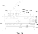
- FIG. 1C illustrates a diagram view of a solder wire bonded on a pad 120 of the semiconductor chip 100 of FIG. 1A
- the semiconductor component 100 is, for example, a semiconductor substrate, a semiconductor chip, etc.
- the semiconductor component 100 includes a substrate 110, at least one pad 120 and a passivation layer 130.
- the substrate 110 includes a base 111, a plurality of conductive layers 112, a plurality of dielectric layers 113 and a plurality of conductive vias 114.
- the base 11 is, for example, silicon wafer.
- the conductive layers 112, the dielectric layers 113 and the conductive vias 114 are formed on the base 111 by using semiconductor processes. Adjacent two conductive layers 112 is separated from each other by one dielectric layers 113 and are electrically connected by at least one conductive via 114.
- the pad 120 could be multi-layered structure.
- the pad 120 includes a pad layer 121 and a barrier layer 122.
- the pad layer 121 is, for example, made of aluminum, gold, silver, copper or combination thereof.
- the barrier layer 122 is, for example, made of nickel (Ni), nickel-alloy, titanium nitride (TiN) or combination thereof. At least one portion of the barrier layer 122 is formed within an opening 113a of the topmost dielectric layer 113, and the pad layer 121 is formed on the barrier layer 122.
- the pad layer 121 is projected with respect to an upper surface 113u of the dielectric layer 113.
- the pad layer 121 has a first lateral surface 121s
- the barrier layer 122 has a second lateral surface 122s, wherein the first lateral surface 121s and the barrier layer 122 are aligned with each other, for example, the first lateral surface 121s and the barrier layer 122 are flush with each other.
- Each pad 120 has an upper surface 120u and a slot 120r, wherein the slot 120r is recessed with respect to the upper surface 120u and extends toward the substrate 110.
- the pad 120 includes a pad portion 121A and a periphery portion 121B, for example, the pad layer 121 of the pad 120 includes the pad portion 121A and the periphery portion 121B, wherein the periphery portion 121B surrounds the pad portion 121A, and the slot 120r is formed between the pad portion 121A and the periphery portion 121B.
- a solder wire 10 is bonded on the corresponding pad 120. After the solder wire 10 is bonded on the pad 120, the solder wire 10 is partially formed within the slot 120r, and at least one portion of the slot 120r is filled with the solder wire 10.
- the slot 120r could provide a deformed portion of the pad portion 121A with space for receiving the deformed portion of the pad portion 121A.
- the slot 120r could receive the deformation (resulted from the pressure being applied by the soldering tool on the pad 120) of the pad portion 121A, and thus it could prevent the pad 120 from cracking or touching adjacent pad due to over-deformation and/or the damage of the passivation layer 130.
- the slot 120r could receive the deformation of the pad portion 121A and/or reduce or release the stress of the pad 120.
- a pitch between adjacent two pads 120 could be shrunk.
- the pitch between adjacent two pad 120 could be shrunk to 5% to 15% compared to pitch between adjacent two pads without slot 121r.
- the slot 120r is a ring-shaped slot, for example, a closed ring-shaped slot or an open ring-shaped slot.
- the slot 120r extends in polygonal shape, circular shape, oval, etc.
- the slot 120r has a width W1 ranging between 0.1 micrometers (mm) and 2.0 mm, for example, 0.1 mm; however, such exemplification is not meant to be for limiting.
- the slot 120r is located between the pad portion 121A and the periphery portion 121B.
- the pad portion 121A is configured to carry the solder wire 10.
- the soldering tool applies force to the pad 120, the pad portion 121A is deformed outwardly, and the slot 120r could receive the deformed pad portion 121A.
- the deformed pad 120 will not touch adjacent pad or adjacent electrical component.
- the passivation layer 130 has at least one opening 130a.
- a first inner sidewall 130w of the opening 130a is aligned with a second inner sidewall 120w of the slot 120r, for example, the first inner sidewall 130w of the opening 130a is flush with the second inner sidewall 120w of the slot 120r.
- FIGS. 2A to 2I illustrate manufacturing processes of the semiconductor component 100 of FIG. 1A .
- a barrier layer material 122" covering the substrate 110 is formed by using deposition technologies.
- the available technologies include but limited to physical vapor deposition (PVD), chemical vapor deposition (CVD), electrochemical deposition (ECD), molecular beam epitaxy (MBE) and more recently, atomic layer deposition (ALD) among others.
- PVD physical vapor deposition
- CVD chemical vapor deposition
- ECD electrochemical deposition
- MBE molecular beam epitaxy
- ALD atomic layer deposition
- a first pad layer material 121" covering the barrier layer material 122" is formed by using back end of line (BEOL) technologies.
- an etching stop structure material 20' covering the first pad layer material 121" is formed by using deposition technologies.
- the available technologies include but limited to physical vapor deposition, chemical vapor deposition, electrochemical deposition, molecular beam epitaxy and more recently, atomic layer deposition (ALD) among others.
- a first patterned photoresist PR1 covering a portion of the etching stop structure material 20' is formed by using deposition technologies.
- the available technologies include but limited to physical vapor deposition, chemical vapor deposition, electrochemical deposition, molecular beam epitaxy and more recently, atomic layer deposition among others.
- the first patterned photoresist PR1 defines a retained portion PR12 and a periphery portion PR11 connected to and surrounding the retained portion PR12.
- the first patterned photoresist PR1 is located right above the opening 113a of the topmost dielectric layer 113.
- a portion of the etching stop structure material 20' is removed to form the etching stop structure 20 through the first patterned photoresist PR1.
- the portion of the etching stop structure material 20' which is not covered by the first patterned photoresist PR1 is removed to form the etching stop structure 20.
- the pad structure 120' further includes the barrier layer material 122".
- the barrier layer material 122" could serve as an etching stop layer, and thus the etching for the first pad layer material 121" (illustrated in FIG. 2A ) could stop at the barrier layer material 122".
- the second pad layer material 121' includes the pad portion 121A' and the periphery portion 121B' connected to and surrounding the pad portion 121A'.
- the etching stop structure 20 and the pad structure 120' are formed in the same etching process through the same first patterned photoresist PR1.
- the periphery portion PR11 of the first patterned photoresist PR1 is removed to expose the periphery portion 21 of the etching stop structure 20 by using etching process.
- the retained portion PR12 of the first patterned photoresist PR1 covering the retained portion 22 of the etching stop structure 20 is retained.
- the periphery portion 21 of the etching stop structure 20 is removed through the retained portion PR12 of the first patterned photoresist PR to expose the periphery portion 121B' of the second pad layer material 121' by using etching process, and the retained portion 22 covering the pad portion 121A' is retained.
- a removed portion 1221" of the barrier layer material 122" is removed to expose the dielectric layer 113 by using etching process, and the barrier layer 122 of the barrier layer material 122" covering the dielectric layer 113 is retained.
- the periphery portion 21 of the etching stop structure 20 and the removed portion 1221" are removed in the same etching process (or simultaneously).
- the pad layer 121 has the first lateral surface 121s
- the barrier layer 122 has the second lateral surface 122s, wherein the first lateral surface 121s and the barrier layer 122 are aligned with each other, for example, the first lateral surface 121s and the barrier layer 122 are flush with each other.
- the retained portion PR12 of the first patterned photoresist PR1 is removed, by using etching process, to expose the retained portion 22 of the etching stop structure 20.
- the passivation layer material 130' covering the retained portion 22, the second pad layer material 121' and the dielectric layer 113 is formed by using deposition technologies.
- the available technologies include but limited to physical vapor deposition (PVD), chemical vapor deposition (CVD), electrochemical deposition (ECD), molecular beam epitaxy (MBE) and more recently, atomic layer deposition (ALD) among others.
- a second patterned photoresist PR2 covering the passivation layer material 130' is formed by using deposition technologies.
- the available technologies include but limited to physical vapor deposition, chemical vapor deposition, electrochemical deposition, molecular beam epitaxy and more recently, atomic layer deposition among others.
- the second patterned photoresist PR2 has at least one opening PR2a exposing a exposed portion 131' of the passivation layer material 130', wherein the exposed portion 131' is located right above the retained portion 22.
- the retained portion 22 has a first width L1
- the opening PR2a has a second width L2, wherein the second width L2 is greater than the first width L1.
- the width difference between the first width L1 and the second width L2 ranges between 0.05 mm and 2 mm.
- an opening 130a is formed on the passivation layer material 130', through the opening PR2a of the second patterned photoresist PR2, to form the passivation layer 130 by using etching process.
- the opening 130 of the passivation layer 130 exposes the pad portion 121A' of the second pad layer material 121' and the retained portion 22, for example, exposes the entire retained portion 22.
- the second patterned photoresist PR2 has an inner sidewall PRs
- the opening 130a of the passivation layer 130 has an inner sidewall 130s, wherein the inner sidewall PRs and the inner sidewall 130s are aligned with each other, for example, the inner sidewall PRs and the inner sidewall 130s are flush with each other.
- a recess 120r' extending from the upper surface 120u (illustrated in FIG. 2G ) of the pad portion 121A' of the second pad layer material 121' toward the substrate 110 through opening PR2a of the second patterned photoresist PR2 and the opening 130a of the passivation layer 130 is formed.
- the recess 120r' has a first depth D1.
- the retained portion 22 of the etching stop structure 20 is removed by using etching process.
- the recess 120r' extends toward the substrate 110 to form the slot 120r'.
- the slot 120r has a second depth D2 greater than the first depth D1 of the recess 120r'.
- the slot 120r is formed and the retained portion 22 is removed. In other words, the slot 120r is formed in process of removing the retained portion 22, and additional photo mask is not needed.
- the second patterned photoresist PR2 is removed to expose the passivation layer 130, and then the semiconductor component 100 is formed.
Landscapes
- Internal Circuitry In Semiconductor Integrated Circuit Devices (AREA)
- Engineering & Computer Science (AREA)
- Manufacturing & Machinery (AREA)
- Wire Bonding (AREA)
Abstract
Description
- The invention relates to a semiconductor component and a manufacturing method thereof, and more particularly to a semiconductor component having a slot and a manufacturing method thereof.
- Conventional semiconductor component includes a number of pads. After a solder wire is bonded on the pad, force is applied to the pad to make the pad crack or deform to touch adjacent pad (cause electrical short).
- In one embodiment of the invention, a semiconductor component is provided. The semiconductor component includes a substrate and a pad. The pad has an upper surface and a slot, wherein the slot is recessed with respect to the upper surface.
- In another embodiment of the invention, a manufacturing method for a semiconductor component is provided. The manufacturing method includes the following steps: forming a pad structure and an etching stop structure on a substrate, wherein the etching stop structure covers the pad structure, wherein the pad structure comprises a pad portion and a periphery portion surrounding the pad portion; removing a periphery portion of the etching stop structure to form a retained portion of the etching stop structure covering the pad portion of the pad structure, wherein the periphery portion of the pad structure is exposed from the retained portion; and forming a slot on the periphery portion of the pad structure to form a pad, wherein the slot is recessed with respect to an upper surface of the pad.
- Numerous objects, features and advantages of the invention will be readily apparent upon a reading of the following detailed description of embodiments of the invention when taken in conjunction with the accompanying drawings. However, the drawings employed herein are for the purpose of descriptions and should not be regarded as limiting.
- The above objects and advantages of the invention will become more readily apparent to those ordinarily skilled in the art after reviewing the following detailed description and accompanying drawings, in which:
-
FIG. 1A illustrates a diagram view of asemiconductor chip 100 according to an embodiment of the invention; -
FIG. 1B illustrates a top view of thesemiconductor chip 100 ofFIG. 1A ; -
FIG. 1C illustrates a diagram view of asolder wire 10 bonded on apad 120 of thesemiconductor chip 100 ofFIG. 1A ; and -
FIGS. 2A to 2I illustrate manufacturing processes of thesemiconductor component 100 ofFIG. 1A . - Referring to
FIGS. 1A to 1C ,FIG. 1A illustrates a diagram view of asemiconductor chip 100 according to an embodiment of the invention,FIG. 1B illustrates a top view of thesemiconductor chip 100 ofFIG. 1A , andFIG. 1C illustrates a diagram view of a solder wire bonded on apad 120 of thesemiconductor chip 100 ofFIG. 1A . In an embodiment, thesemiconductor component 100 is, for example, a semiconductor substrate, a semiconductor chip, etc. - The
semiconductor component 100 includes asubstrate 110, at least onepad 120 and apassivation layer 130. - The
substrate 110 includes abase 111, a plurality ofconductive layers 112, a plurality ofdielectric layers 113 and a plurality ofconductive vias 114. The base 11 is, for example, silicon wafer. Theconductive layers 112, thedielectric layers 113 and theconductive vias 114 are formed on thebase 111 by using semiconductor processes. Adjacent twoconductive layers 112 is separated from each other by onedielectric layers 113 and are electrically connected by at least one conductive via 114. - As illustrated in
FIG. 1A , thepad 120 could be multi-layered structure. For example, thepad 120 includes apad layer 121 and abarrier layer 122. Thepad layer 121 is, for example, made of aluminum, gold, silver, copper or combination thereof. Thebarrier layer 122 is, for example, made of nickel (Ni), nickel-alloy, titanium nitride (TiN) or combination thereof. At least one portion of thebarrier layer 122 is formed within an opening 113a of the topmostdielectric layer 113, and thepad layer 121 is formed on thebarrier layer 122. Thepad layer 121 is projected with respect to anupper surface 113u of thedielectric layer 113. Thepad layer 121 has a firstlateral surface 121s, and thebarrier layer 122 has a secondlateral surface 122s, wherein the firstlateral surface 121s and thebarrier layer 122 are aligned with each other, for example, the firstlateral surface 121s and thebarrier layer 122 are flush with each other. - Each
pad 120 has anupper surface 120u and aslot 120r, wherein theslot 120r is recessed with respect to theupper surface 120u and extends toward thesubstrate 110. Thepad 120 includes apad portion 121A and aperiphery portion 121B, for example, thepad layer 121 of thepad 120 includes thepad portion 121A and theperiphery portion 121B, wherein theperiphery portion 121B surrounds thepad portion 121A, and theslot 120r is formed between thepad portion 121A and theperiphery portion 121B. - As illustrated in
FIG. 1C , asolder wire 10 is bonded on thecorresponding pad 120. After thesolder wire 10 is bonded on thepad 120, thesolder wire 10 is partially formed within theslot 120r, and at least one portion of theslot 120r is filled with thesolder wire 10. Theslot 120r could provide a deformed portion of thepad portion 121A with space for receiving the deformed portion of thepad portion 121A. Furthermore, during thesolder wire 10 is bonded on thepad 120, theslot 120r could receive the deformation (resulted from the pressure being applied by the soldering tool on the pad 120) of thepad portion 121A, and thus it could prevent thepad 120 from cracking or touching adjacent pad due to over-deformation and/or the damage of thepassivation layer 130. In other words, theslot 120r could receive the deformation of thepad portion 121A and/or reduce or release the stress of thepad 120. As a result, a pitch between adjacent twopads 120 could be shrunk. In an embodiment, the pitch between adjacent twopad 120 could be shrunk to 5% to 15% compared to pitch between adjacent two pads without slot 121r. - As illustrated in
FIG. 1B , theslot 120r is a ring-shaped slot, for example, a closed ring-shaped slot or an open ring-shaped slot. In addition, theslot 120r extends in polygonal shape, circular shape, oval, etc. Theslot 120r has a width W1 ranging between 0.1 micrometers (mm) and 2.0 mm, for example, 0.1 mm; however, such exemplification is not meant to be for limiting. - As illustrated in
FIG. 1C , theslot 120r is located between thepad portion 121A and theperiphery portion 121B. Thepad portion 121A is configured to carry thesolder wire 10. When the soldering tool applies force to thepad 120, thepad portion 121A is deformed outwardly, and theslot 120r could receive thedeformed pad portion 121A. As a result, even if thepad 120 deforms, thedeformed pad 120 will not touch adjacent pad or adjacent electrical component. - As illustrated in
FIG. 1A , thepassivation layer 130 has at least oneopening 130a. A firstinner sidewall 130w of theopening 130a is aligned with a secondinner sidewall 120w of theslot 120r, for example, the firstinner sidewall 130w of theopening 130a is flush with the secondinner sidewall 120w of theslot 120r. -
FIGS. 2A to 2I illustrate manufacturing processes of thesemiconductor component 100 ofFIG. 1A . - As illustrated in
FIG. 2A , abarrier layer material 122" covering thesubstrate 110 is formed by using deposition technologies. The available technologies include but limited to physical vapor deposition (PVD), chemical vapor deposition (CVD), electrochemical deposition (ECD), molecular beam epitaxy (MBE) and more recently, atomic layer deposition (ALD) among others. Then, a firstpad layer material 121" covering thebarrier layer material 122" is formed by using back end of line (BEOL) technologies. Then, an etching stop structure material 20' covering the firstpad layer material 121" is formed by using deposition technologies. The available technologies include but limited to physical vapor deposition, chemical vapor deposition, electrochemical deposition, molecular beam epitaxy and more recently, atomic layer deposition (ALD) among others. - Then, as illustrated in
FIG. 2A , a first patterned photoresist PR1 covering a portion of the etching stop structure material 20' is formed by using deposition technologies. The available technologies include but limited to physical vapor deposition, chemical vapor deposition, electrochemical deposition, molecular beam epitaxy and more recently, atomic layer deposition among others. The first patterned photoresist PR1 defines a retained portion PR12 and a periphery portion PR11 connected to and surrounding the retained portion PR12. The first patterned photoresist PR1 is located right above theopening 113a of the topmostdielectric layer 113. - Then, as illustrated in
FIG. 2B , a portion of the etching stop structure material 20' is removed to form theetching stop structure 20 through the first patterned photoresist PR1. For example, the portion of the etching stop structure material 20' which is not covered by the first patterned photoresist PR1 is removed to form theetching stop structure 20. - As illustrated in
FIG. 2B , a portion of the firstpad layer material 121" is removed to form a second pad layer material 121' of a pad structure 120' through the first patterned photoresist PR1 by using etching technology. The pad structure 120' further includes thebarrier layer material 122". In the present embodiment, thebarrier layer material 122" could serve as an etching stop layer, and thus the etching for the firstpad layer material 121" (illustrated inFIG. 2A ) could stop at thebarrier layer material 122". As illustrated inFIG. 2B , the second pad layer material 121' includes thepad portion 121A' and theperiphery portion 121B' connected to and surrounding thepad portion 121A'. - In the present embodiment, the
etching stop structure 20 and the pad structure 120' are formed in the same etching process through the same first patterned photoresist PR1. - As illustrated in FIC. 2C, the periphery portion PR11 of the first patterned photoresist PR1 is removed to expose the
periphery portion 21 of theetching stop structure 20 by using etching process. In etching process, the retained portion PR12 of the first patterned photoresist PR1 covering the retainedportion 22 of theetching stop structure 20 is retained. - As illustrated in
FIG.2D , theperiphery portion 21 of theetching stop structure 20 is removed through the retained portion PR12 of the first patterned photoresist PR to expose theperiphery portion 121B' of the second pad layer material 121' by using etching process, and the retainedportion 22 covering thepad portion 121A' is retained. - In
FIG. 2D , a removedportion 1221" of thebarrier layer material 122" is removed to expose thedielectric layer 113 by using etching process, and thebarrier layer 122 of thebarrier layer material 122" covering thedielectric layer 113 is retained. - In an embodiment, the
periphery portion 21 of theetching stop structure 20 and the removedportion 1221" are removed in the same etching process (or simultaneously). In addition, after etching, thepad layer 121 has the firstlateral surface 121s, and thebarrier layer 122 has the secondlateral surface 122s, wherein the firstlateral surface 121s and thebarrier layer 122 are aligned with each other, for example, the firstlateral surface 121s and thebarrier layer 122 are flush with each other. - As illustrated in
FIG. 2E , the retained portion PR12 of the first patterned photoresist PR1 is removed, by using etching process, to expose the retainedportion 22 of theetching stop structure 20. - As illustrated in
FIG. 2F , the passivation layer material 130' covering the retainedportion 22, the second pad layer material 121' and thedielectric layer 113 is formed by using deposition technologies. The available technologies include but limited to physical vapor deposition (PVD), chemical vapor deposition (CVD), electrochemical deposition (ECD), molecular beam epitaxy (MBE) and more recently, atomic layer deposition (ALD) among others. - As illustrated in
FIG. 2G , a second patterned photoresist PR2 covering the passivation layer material 130' is formed by using deposition technologies. The available technologies include but limited to physical vapor deposition, chemical vapor deposition, electrochemical deposition, molecular beam epitaxy and more recently, atomic layer deposition among others. The second patterned photoresist PR2 has at least one opening PR2a exposing a exposed portion 131' of the passivation layer material 130', wherein the exposed portion 131' is located right above the retainedportion 22. - In
FIG. 2G , the retainedportion 22 has a first width L1, and the opening PR2a has a second width L2, wherein the second width L2 is greater than the first width L1. For example, the width difference between the first width L1 and the second width L2 ranges between 0.05 mm and 2 mm. - As illustrated in
FIG. 2H , anopening 130a is formed on the passivation layer material 130', through the opening PR2a of the second patterned photoresist PR2, to form thepassivation layer 130 by using etching process. Theopening 130 of thepassivation layer 130 exposes thepad portion 121A' of the second pad layer material 121' and the retainedportion 22, for example, exposes the entire retainedportion 22. After etching, the second patterned photoresist PR2 has an inner sidewall PRs, and theopening 130a of thepassivation layer 130 has aninner sidewall 130s, wherein the inner sidewall PRs and theinner sidewall 130s are aligned with each other, for example, the inner sidewall PRs and theinner sidewall 130s are flush with each other. - In
FIG. 2H , in etching process, arecess 120r' extending from theupper surface 120u (illustrated inFIG. 2G ) of thepad portion 121A' of the second pad layer material 121' toward thesubstrate 110 through opening PR2a of the second patterned photoresist PR2 and theopening 130a of thepassivation layer 130 is formed. Therecess 120r' has a first depth D1. - As illustrated in
FIG. 2I , the retainedportion 22 of theetching stop structure 20 is removed by using etching process. In etching process, therecess 120r' extends toward thesubstrate 110 to form theslot 120r'. Theslot 120r has a second depth D2 greater than the first depth D1 of therecess 120r'. In same etching process, theslot 120r is formed and the retainedportion 22 is removed. In other words, theslot 120r is formed in process of removing the retainedportion 22, and additional photo mask is not needed. - Then, the second patterned photoresist PR2 is removed to expose the
passivation layer 130, and then thesemiconductor component 100 is formed. - While the invention has been described in terms of what is presently considered to be the most practical and preferred embodiments, it is to be understood that the invention needs not be limited to the disclosed embodiment. On the contrary, it is intended to cover various modifications and similar arrangements included within the spirit and scope of the appended claims which are to be accorded with the broadest interpretation so as to encompass all such modifications and similar structures.
Claims (15)
- A semiconductor component (100), comprising:a substrate (110); anda pad (120) having an upper surface (120u) and a slot (120r, 120r');wherein the slot (120r, 120r') is recessed with respect to the upper surface (120u).
- The semiconductor component (100) as claimed in claim 1, further comprises:a passivation layer (130) having an opening (130a);wherein a first inner sidewall (130w) of the opening (130a) is aligned with a second inner sidewall (120w) of the slot (120r, 120r').
- The semiconductor component (100) as claimed in claim 1, wherein the pad (120) comprises a pad portion (121A) and a periphery portion (121B) surrounding the pad portion (121A), and the slot (120r, 120r') is located between the pad portion (121A) and the periphery portion (121B).
- The semiconductor component (100) as claimed in claim 1, wherein the slot (120r, 120r') is a ring-shaped slot.
- The semiconductor component (100) as claimed in claim 4, wherein the slot (120r, 120r') is a closed ring-shaped slot.
- The semiconductor component (100) as claimed in claim 1, wherein the slot (120r, 120r') has a width ranging between 0.1 micrometers and 2.0 micrometers.
- The semiconductor component (100) as claimed in claim 1, further comprises:
a solder wire (10) partially formed within the slot (120r, 120r'). - The semiconductor component (100) as claimed in claim 7, wherein at least one portion of the slot (120r, 120r') is filled with the solder wire (10).
- A manufacturing method for a semiconductor component (100), comprising:forming a pad structure (120') and an etching stop structure (20) on a substrate (110), wherein the etching stop structure (20) covers the pad structure (120'), wherein the pad structure (120') comprises a pad portion (121A) and a periphery portion (121B) surrounding the pad portion (121A) ;removing a periphery portion (21) of the etching stop structure (20) to form a retained portion (22) of the etching stop structure (20) covering the pad portion (121A) of the pad structure (120'), wherein the periphery portion (121B') of the pad structure (120') is exposed from the retained portion (22); andforming a slot (120r, 120r') on the periphery portion (121B') of the pad structure (120') to form a pad (120), wherein the slot (120r, 120r') is recessed with respect to an upper surface (120u) of the pad (120).
- The manufacturing method as claimed in claim 9, further comprises:forming a barrier layer material (122") on the substrate (110);forming a first pad layer material (121") to cover the barrier layer material (122");forming an etching stop structure material (20') to cover the first pad layer material (121");removing a portion of the first pad layer material (121") to form a second pad layer material (121') of the pad structure (120'), wherein the second pad layer material (121') comprises the pad portion (121A) and the periphery portion (121B); andremoving a portion of the etching stop structure material (20') to form the etching stop structure (20).
- The manufacturing method as claimed in claim 10, wherein in step of removing the portion of the first pad layer material (121") to form the second pad layer material (121') of the pad structure (120') comprises:forming a first patterned photoresist (PR1) to cover the etching stop structure material (20');removing the portion of the first pad layer material (121"), through the first patterned photoresist (PR1), to form the second pad layer material (121') of the pad structure (120');wherein in step of removing the portion of the etching stop structure material (20') to form the etching stop structure (20) comprises:
removing the portion of the etching stop structure material (20'), through the first patterned photoresist (PR1), to form the etching stop structure (20). - The manufacturing method as claimed in claim 11, further comprises:removing a periphery portion (PR11) of the first patterned photoresist (PR1), wherein a retained portion (PR12) of the first patterned photoresist (PR1) covering the retained portion (PR12) of the etching stop structure (20) is retained;wherein in step of removing the periphery portion (21) of the etching stop structure (20) to form the retained portion (22) of the etching stop structure (20) covering the pad portion (121A) of the pad structure (120') further comprises:removing the periphery portion (21) of the etching stop structure (20), through the retained portion (PR12) of the first patterned photoresist (PR1), to form the retained portion (22) of the etching stop structure (20) and expose the periphery portion (121B') of the second pad layer material (121'); andremoving the first patterned photoresist (PR1) to expose the retained portion (22) of the etching stop structure (20).
- The manufacturing method as claimed in claim 10, further comprises:
removing a removed portion (1221") of the barrier layer material (122") to form a barrier layer of the pad (120) covered by the pad portion (121A). - The manufacturing method as claimed in claim 13, wherein step of removing the removed portion (1221") of the barrier layer material (122") and step of removing a periphery portion (21) of the etching stop structure (20) are performed in the same process.
- The manufacturing method as claimed in claim 9, further comprises:forming a passivation layer (130) material to cover the retained portion (22) of the etching stop structure (20);forming an opening (130a) on the passivation layer material (130'); andforming a recess (120r') to extend from the upper surface (120u) of the pad (120) toward the substrate (110).
Applications Claiming Priority (2)
| Application Number | Priority Date | Filing Date | Title |
|---|---|---|---|
| US201962887075P | 2019-08-15 | 2019-08-15 | |
| US16/928,089 US11424204B2 (en) | 2019-08-15 | 2020-07-14 | Semiconductor component and manufacturing method thereof |
Publications (1)
| Publication Number | Publication Date |
|---|---|
| EP3780093A1 true EP3780093A1 (en) | 2021-02-17 |
Family
ID=71899507
Family Applications (1)
| Application Number | Title | Priority Date | Filing Date |
|---|---|---|---|
| EP20188651.2A Pending EP3780093A1 (en) | 2019-08-15 | 2020-07-30 | Semiconductor component and manufacturing method thereof |
Country Status (4)
| Country | Link |
|---|---|
| US (1) | US11424204B2 (en) |
| EP (1) | EP3780093A1 (en) |
| CN (1) | CN112397469B (en) |
| TW (1) | TWI742780B (en) |
Families Citing this family (2)
| Publication number | Priority date | Publication date | Assignee | Title |
|---|---|---|---|---|
| TWI855778B (en) * | 2023-07-18 | 2024-09-11 | 南亞科技股份有限公司 | Semiconductor device and method of manufacturing the same |
| TWI879662B (en) * | 2023-07-18 | 2025-04-01 | 南亞科技股份有限公司 | Semiconductor device and method of manufacturing the same |
Citations (5)
| Publication number | Priority date | Publication date | Assignee | Title |
|---|---|---|---|---|
| US6287950B1 (en) * | 2000-02-03 | 2001-09-11 | Taiwan Semiconductor Manufacturing Co., Ltd. | Bonding pad structure and manufacturing method thereof |
| US20080197353A1 (en) * | 2007-02-21 | 2008-08-21 | Fujitsu Limited | Semiconductor device for which electrical test is performed while probe is in contact with conductive pad |
| US20130234309A1 (en) * | 2012-03-08 | 2013-09-12 | Renesas Electronics Corporation | Semiconductor device |
| US20150194395A1 (en) * | 2014-01-03 | 2015-07-09 | Sohrab Safai | Bond pad having a trench and method for forming |
| JP2016167536A (en) * | 2015-03-10 | 2016-09-15 | セイコーエプソン株式会社 | Electronic component and manufacturing method thereof |
Family Cites Families (8)
| Publication number | Priority date | Publication date | Assignee | Title |
|---|---|---|---|---|
| US6825541B2 (en) * | 2002-10-09 | 2004-11-30 | Taiwan Semiconductor Manufacturing Co., Ltd | Bump pad design for flip chip bumping |
| US6844626B2 (en) * | 2003-05-23 | 2005-01-18 | Taiwan Semiconductor Manufacturing Company, Ltd. | Bond pad scheme for Cu process |
| US7585754B2 (en) * | 2008-01-10 | 2009-09-08 | Winbond Electronics Corp. | Method of forming bonding pad opening |
| US9515034B2 (en) * | 2014-01-03 | 2016-12-06 | Freescale Semiconductor, Inc. | Bond pad having a trench and method for forming |
| JP6301763B2 (en) * | 2014-07-16 | 2018-03-28 | ルネサスエレクトロニクス株式会社 | Semiconductor device and manufacturing method of semiconductor device |
| US9704827B2 (en) * | 2015-06-25 | 2017-07-11 | Taiwan Semiconductor Manufacturing Co., Ltd. | Hybrid bond pad structure |
| US10038025B2 (en) | 2015-12-29 | 2018-07-31 | Taiwan Semiconductor Manufacturing Co., Ltd. | Via support structure under pad areas for BSI bondability improvement |
| US10109666B2 (en) | 2016-04-13 | 2018-10-23 | Taiwan Semiconductor Manufacturing Co., Ltd. | Pad structure for backside illuminated (BSI) image sensors |
-
2020
- 2020-07-14 US US16/928,089 patent/US11424204B2/en active Active
- 2020-07-23 CN CN202010716324.0A patent/CN112397469B/en active Active
- 2020-07-27 TW TW109125328A patent/TWI742780B/en active
- 2020-07-30 EP EP20188651.2A patent/EP3780093A1/en active Pending
Patent Citations (5)
| Publication number | Priority date | Publication date | Assignee | Title |
|---|---|---|---|---|
| US6287950B1 (en) * | 2000-02-03 | 2001-09-11 | Taiwan Semiconductor Manufacturing Co., Ltd. | Bonding pad structure and manufacturing method thereof |
| US20080197353A1 (en) * | 2007-02-21 | 2008-08-21 | Fujitsu Limited | Semiconductor device for which electrical test is performed while probe is in contact with conductive pad |
| US20130234309A1 (en) * | 2012-03-08 | 2013-09-12 | Renesas Electronics Corporation | Semiconductor device |
| US20150194395A1 (en) * | 2014-01-03 | 2015-07-09 | Sohrab Safai | Bond pad having a trench and method for forming |
| JP2016167536A (en) * | 2015-03-10 | 2016-09-15 | セイコーエプソン株式会社 | Electronic component and manufacturing method thereof |
Non-Patent Citations (1)
| Title |
|---|
| ANONYMOUS: "Hardmask - Wikipedia", 16 July 2022 (2022-07-16), XP093159668, Retrieved from the Internet <URL:https://en.wikipedia.org/w/index.php?title=Hardmask&oldid=1098536422> [retrieved on 20240506] * |
Also Published As
| Publication number | Publication date |
|---|---|
| TWI742780B (en) | 2021-10-11 |
| TW202110296A (en) | 2021-03-01 |
| US20210050315A1 (en) | 2021-02-18 |
| CN112397469A (en) | 2021-02-23 |
| CN112397469B (en) | 2024-09-27 |
| US11424204B2 (en) | 2022-08-23 |
Similar Documents
| Publication | Publication Date | Title |
|---|---|---|
| US6518092B2 (en) | Semiconductor device and method for manufacturing | |
| US8421238B2 (en) | Stacked semiconductor device with through via | |
| JP4873517B2 (en) | Semiconductor device and manufacturing method thereof | |
| CN1777978B (en) | Reduce metal in wafer dicing area | |
| JP4373866B2 (en) | Manufacturing method of semiconductor device | |
| US10276510B2 (en) | Manufacturing method of package structure having conductive shield | |
| US20070269931A1 (en) | Wafer level package and method of fabricating the same | |
| KR20200068958A (en) | Connection structure and method of forming the same | |
| US10607860B2 (en) | Package structure and chip structure | |
| TW201719842A (en) | Semiconductor component structure and method of forming same | |
| JP2010045371A (en) | Through-silicon-via structure including conductive protective film, and method of forming the same | |
| JP2002289623A (en) | Semiconductor device and manufacturing method thereof | |
| JP2018157110A (en) | Semiconductor device and manufacturing method for the same | |
| US11424204B2 (en) | Semiconductor component and manufacturing method thereof | |
| US10950525B2 (en) | Fabrication method of packaging structure | |
| US11545469B2 (en) | Semiconductor package and manufacturing method thereof | |
| US9515034B2 (en) | Bond pad having a trench and method for forming | |
| KR20220028310A (en) | Interconnection structure, method of forming the same, and semiconductor package including the interconnection structure | |
| US20070123021A1 (en) | Circuit under pad structure and bonding pad process | |
| CN112582364B (en) | Pad structure and forming method thereof, semiconductor device and forming method thereof | |
| US20210242149A1 (en) | Semiconductor structure, redistribution layer (rdl) structure, and manufacturing method thereof | |
| US12354961B2 (en) | Semiconductor structure and manufacturing method thereof | |
| US20250210415A1 (en) | Manufacturing method of semiconductor structure | |
| EP4084053B1 (en) | Semiconductor structure and its method for manufacturing | |
| US20260018493A1 (en) | Semiconductor structure |
Legal Events
| Date | Code | Title | Description |
|---|---|---|---|
| PUAI | Public reference made under article 153(3) epc to a published international application that has entered the european phase |
Free format text: ORIGINAL CODE: 0009012 |
|
| STAA | Information on the status of an ep patent application or granted ep patent |
Free format text: STATUS: REQUEST FOR EXAMINATION WAS MADE |
|
| 17P | Request for examination filed |
Effective date: 20200730 |
|
| AK | Designated contracting states |
Kind code of ref document: A1 Designated state(s): AL AT BE BG CH CY CZ DE DK EE ES FI FR GB GR HR HU IE IS IT LI LT LU LV MC MK MT NL NO PL PT RO RS SE SI SK SM TR |
|
| AX | Request for extension of the european patent |
Extension state: BA ME |
|
| RBV | Designated contracting states (corrected) |
Designated state(s): AL AT BE BG CH CY CZ DE DK EE ES FI FR GB GR HR HU IE IS IT LI LT LU LV MC MK MT NL NO PL PT RO RS SE SI SK SM TR |
|
| P01 | Opt-out of the competence of the unified patent court (upc) registered |
Effective date: 20230607 |
|
| STAA | Information on the status of an ep patent application or granted ep patent |
Free format text: STATUS: EXAMINATION IS IN PROGRESS |
|
| 17Q | First examination report despatched |
Effective date: 20240513 |