EP3772810A1 - Dc link capacitor pre-charge method utilizing series boost converter - Google Patents
Dc link capacitor pre-charge method utilizing series boost converter Download PDFInfo
- Publication number
- EP3772810A1 EP3772810A1 EP19275087.5A EP19275087A EP3772810A1 EP 3772810 A1 EP3772810 A1 EP 3772810A1 EP 19275087 A EP19275087 A EP 19275087A EP 3772810 A1 EP3772810 A1 EP 3772810A1
- Authority
- EP
- European Patent Office
- Prior art keywords
- power
- link capacitor
- charge
- load
- power supply
- Prior art date
- Legal status (The legal status is an assumption and is not a legal conclusion. Google has not performed a legal analysis and makes no representation as to the accuracy of the status listed.)
- Granted
Links
Images


Classifications
-
- H—ELECTRICITY
- H02—GENERATION; CONVERSION OR DISTRIBUTION OF ELECTRIC POWER
- H02M—APPARATUS FOR CONVERSION BETWEEN AC AND AC, BETWEEN AC AND DC, OR BETWEEN DC AND DC, AND FOR USE WITH MAINS OR SIMILAR POWER SUPPLY SYSTEMS; CONVERSION OF DC OR AC INPUT POWER INTO SURGE OUTPUT POWER; CONTROL OR REGULATION THEREOF
- H02M5/00—Conversion of AC power input into AC power output, e.g. for change of voltage, for change of frequency, for change of number of phases
- H02M5/40—Conversion of AC power input into AC power output, e.g. for change of voltage, for change of frequency, for change of number of phases with intermediate conversion into DC
- H02M5/42—Conversion of AC power input into AC power output, e.g. for change of voltage, for change of frequency, for change of number of phases with intermediate conversion into DC by static converters
- H02M5/44—Conversion of AC power input into AC power output, e.g. for change of voltage, for change of frequency, for change of number of phases with intermediate conversion into DC by static converters using discharge tubes or semiconductor devices to convert the intermediate DC into AC
- H02M5/453—Conversion of AC power input into AC power output, e.g. for change of voltage, for change of frequency, for change of number of phases with intermediate conversion into DC by static converters using discharge tubes or semiconductor devices to convert the intermediate DC into AC using devices of a triode or transistor type requiring continuous application of a control signal
- H02M5/458—Conversion of AC power input into AC power output, e.g. for change of voltage, for change of frequency, for change of number of phases with intermediate conversion into DC by static converters using discharge tubes or semiconductor devices to convert the intermediate DC into AC using devices of a triode or transistor type requiring continuous application of a control signal using semiconductor devices only
-
- H—ELECTRICITY
- H02—GENERATION; CONVERSION OR DISTRIBUTION OF ELECTRIC POWER
- H02M—APPARATUS FOR CONVERSION BETWEEN AC AND AC, BETWEEN AC AND DC, OR BETWEEN DC AND DC, AND FOR USE WITH MAINS OR SIMILAR POWER SUPPLY SYSTEMS; CONVERSION OF DC OR AC INPUT POWER INTO SURGE OUTPUT POWER; CONTROL OR REGULATION THEREOF
- H02M1/00—Details of apparatus for conversion
- H02M1/36—Means for starting or stopping converters
-
- H—ELECTRICITY
- H02—GENERATION; CONVERSION OR DISTRIBUTION OF ELECTRIC POWER
- H02M—APPARATUS FOR CONVERSION BETWEEN AC AND AC, BETWEEN AC AND DC, OR BETWEEN DC AND DC, AND FOR USE WITH MAINS OR SIMILAR POWER SUPPLY SYSTEMS; CONVERSION OF DC OR AC INPUT POWER INTO SURGE OUTPUT POWER; CONTROL OR REGULATION THEREOF
- H02M7/00—Conversion of AC power input into DC power output; Conversion of DC power input into AC power output
- H02M7/02—Conversion of AC power input into DC power output without possibility of reversal
- H02M7/04—Conversion of AC power input into DC power output without possibility of reversal by static converters
- H02M7/06—Conversion of AC power input into DC power output without possibility of reversal by static converters using discharge tubes without control electrode or semiconductor devices without control electrode
- H02M7/062—Avoiding or suppressing excessive transient voltages or currents
-
- H—ELECTRICITY
- H02—GENERATION; CONVERSION OR DISTRIBUTION OF ELECTRIC POWER
- H02M—APPARATUS FOR CONVERSION BETWEEN AC AND AC, BETWEEN AC AND DC, OR BETWEEN DC AND DC, AND FOR USE WITH MAINS OR SIMILAR POWER SUPPLY SYSTEMS; CONVERSION OF DC OR AC INPUT POWER INTO SURGE OUTPUT POWER; CONTROL OR REGULATION THEREOF
- H02M1/00—Details of apparatus for conversion
- H02M1/0064—Magnetic structures combining different functions, e.g. storage, filtering or transformation
-
- H—ELECTRICITY
- H02—GENERATION; CONVERSION OR DISTRIBUTION OF ELECTRIC POWER
- H02M—APPARATUS FOR CONVERSION BETWEEN AC AND AC, BETWEEN AC AND DC, OR BETWEEN DC AND DC, AND FOR USE WITH MAINS OR SIMILAR POWER SUPPLY SYSTEMS; CONVERSION OF DC OR AC INPUT POWER INTO SURGE OUTPUT POWER; CONTROL OR REGULATION THEREOF
- H02M3/00—Conversion of DC power input into DC power output
- H02M3/22—Conversion of DC power input into DC power output with intermediate conversion into AC
- H02M3/24—Conversion of DC power input into DC power output with intermediate conversion into AC by static converters
- H02M3/28—Conversion of DC power input into DC power output with intermediate conversion into AC by static converters using discharge tubes with control electrode or semiconductor devices with control electrode to produce the intermediate AC
- H02M3/325—Conversion of DC power input into DC power output with intermediate conversion into AC by static converters using discharge tubes with control electrode or semiconductor devices with control electrode to produce the intermediate AC using devices of a triode or a transistor type requiring continuous application of a control signal
- H02M3/335—Conversion of DC power input into DC power output with intermediate conversion into AC by static converters using discharge tubes with control electrode or semiconductor devices with control electrode to produce the intermediate AC using devices of a triode or a transistor type requiring continuous application of a control signal using semiconductor devices only
- H02M3/33507—Conversion of DC power input into DC power output with intermediate conversion into AC by static converters using discharge tubes with control electrode or semiconductor devices with control electrode to produce the intermediate AC using devices of a triode or a transistor type requiring continuous application of a control signal using semiconductor devices only with automatic control of the output voltage or current, e.g. flyback converters
-
- H—ELECTRICITY
- H02—GENERATION; CONVERSION OR DISTRIBUTION OF ELECTRIC POWER
- H02M—APPARATUS FOR CONVERSION BETWEEN AC AND AC, BETWEEN AC AND DC, OR BETWEEN DC AND DC, AND FOR USE WITH MAINS OR SIMILAR POWER SUPPLY SYSTEMS; CONVERSION OF DC OR AC INPUT POWER INTO SURGE OUTPUT POWER; CONTROL OR REGULATION THEREOF
- H02M5/00—Conversion of AC power input into AC power output, e.g. for change of voltage, for change of frequency, for change of number of phases
- H02M5/40—Conversion of AC power input into AC power output, e.g. for change of voltage, for change of frequency, for change of number of phases with intermediate conversion into DC
- H02M5/42—Conversion of AC power input into AC power output, e.g. for change of voltage, for change of frequency, for change of number of phases with intermediate conversion into DC by static converters
- H02M5/44—Conversion of AC power input into AC power output, e.g. for change of voltage, for change of frequency, for change of number of phases with intermediate conversion into DC by static converters using discharge tubes or semiconductor devices to convert the intermediate DC into AC
Definitions
- a power train comprising a load, a first power supply for providing power to the load; a DC-link capacitor connected to the load; a main converter configured to convert DC power to AC power for powering the load; and pre-charge circuitry comprising pre-charge means configured to, during a first, pre-charge phase, prevent said power from being provided to said load but provide power to said DC-link capacitor to charge said DC-link capacitor, and, further configured to, during a second, post-charge phase, allow said power to be provided from said first power supply to said load.
- the DC-link capacitor may be connected in parallel with the load.
- the power train may further comprise a rectifier unit configured to convert AC power from the first power supply to DC power; and a main converter configured to convert DC power to AC power for powering the load.
- the DC link Capacitor may be connected between said rectifier unit and the main converter to facilitate proper commutation (switching) in the main converter and/or de-couple the main converter from the rectifier.
- the converter may be configured to facilitate and/or control the power into load.
- This power can be of a DC or AC nature. In the case of AC, power can be supplied to the load by a single or any polyphase system.
- the pre-charge circuitry may further comprise a power converter, a second power supply and said pre-charge means may comprise a transformer.
- the transformer may comprise an inductor connected in series with the first power supply and the DC-link capacitor.
- the inductor may comprise a primary winding of the transformer.
- the transformer may further comprise a secondary winding electrically connected to the power converter and the power supply.
- the power train may further comprise a rectifier unit configured to convert AC power from said first power means to DC power.
- the power train may further comprise a diode connected in parallel with the DC-link capacitor.
- a method of providing power to a load comprising connecting a first power supply to the load, connecting a DC-link capacitor to the load and providing pre-charge circuitry.
- the pre-charge circuitry may comprise pre-charge means configured to, during a first, pre-charge phase, prevent said power from being provided to said load but provide power to said DC-link capacitor to charge said DC-link capacitor, and, further configured to, during a second, post-charge phase, allow said power to be provided from said first power supply to said load.
- the step of connecting said DC-link capacitor to said load may comprise connecting said DC-link capacitor in parallel with the load.
- the method may further comprise providing, in said pre-charge circuitry, a power converter, a second power supply and the pre-charge means may comprises a transformer.
- the transformer may comprise an inductor and the method may further comprise connecting said inductor in series with the first power supply and the DC-link capacitor.
- the transformer may comprise a primary winding and a secondary winding and the inductor may be the primary winding of the transformer.
- the secondary winding may be electrically connected to the power converter and the power supply.
- the method may further comprise inducing power in the inductor by providing said power to said secondary winding, wherein the induced power charges said DC-link capacitor.
- the inductor and the DC-link capacitor may act as a filter section.
- the step of pre-charging the DC-link capacitor may comprise charging the DC-link capacitor to a first, desired voltage level.
- said first, desired voltage level may be 240Vdc, although the examples are not limited to this.
- DC-AC conversion circuits typically include inductive components for EMI filtering and power quality performance.
- FIG. 1 A typical, known, power train that may be used in aircraft is presented in Figure 1 . It consists of a generator 1, a rectifier unit 2, a pre-charge circuitry 3, a filter section 4, a converter 5, and a load 6.
- the pre-charge functionality of the circuitry 3 is required to limit the initial in-rush current which shares capacitors in filter section 4. These limits of initial inrush current are defined by aerospace standard or individual customer requirements.
- a typical example of a known pre-charge circuitry 3 consists of a power electronics switch 3a connected in parallel with a resistor 3b.
- switch 3a During the initial in-rush current that occurs when the 3-phase voltage from the generator 1 is applied to the power circuit, switch 3a remains open which causes the current flowing through the DC link capacitor to be limited by the resistor 3b.
- switch 3a When the pre-charge is completed, switch 3a is closed, thereby bypassing resistor 3b.
- thyristor or MOSFET switches are used as the switching device.
- pre-charge circuitry 3 Alternative approaches to pre-charge circuitry 3 have been considered.
- Figure 2 shows the use of a parallel boost converter.
- an output of the boost converter 7 is connected in parallel with the DC link capacitor, with the boost converter 7 being charged from the low voltage source 8 (for example, a battery).
- the low voltage source 8 for example, a battery
- Pre-charge circuits based on capacitive voltage dividers have also been utilised, as seen in Figure 4 .
- they are very similar to buck converter based pre-charge circuits, although they offer a safe power train disconnect in case of a fault.
- capacitive voltage dividers 9a are connected in series with DC link capacitor and bypassed with power electronics switch 10 when the pre-charge phase is finished.
- these again suffer from an efficiency loss due power electronic switch 10 caused by conduction losses.
- some existing solutions typically use a resistor to limit the inrush current and a parallel shorting switch (thyristor or MOSFET). Following the pre-charge operation, the shorting switch is turned on, shorting the resistor for normal operation.
- the new types of devices and methods described herein eliminate the power losses of the parallel switch, thereby improving circuit efficiency and reducing heat sink mass. They also make use of existing magnetic components for reduced complexity.
- the new examples described herein modify this existing inductive element with a secondary winding to form a transformer.
- the primary winding is connected as in known devices so that in normal operation the inductor performs its primary filtering function.
- the secondary winding is connected to a small power converter that can be operated from an auxiliary supply.
- the secondary winding is excited with the small power converter to gradually charge the DC link capacitor. Once charged, the small converter is disabled, high voltage can be connected to the main circuit and normal operation commences, preventing a damaging inrush current.
- a power train may be provided comprising a generator 1, a rectifier unit 2, pre-charge circuitry 11, a converter 5, and a load 6.
- Pre-charge circuitry 11 may comprise a transformer 12 (comprising a primary winding 121 and a secondary winding 122), a power converter 13 and a power supply 14. Further, in some examples, the pre-charge circuitry 11 may optionally comprise a diode 15, if the power train is powered from a DC source.
- the primary winding 121 of transformer 12 is connected in series with the power supply and the DC link capacitor 111. After pre-charge, this primary winding 121 is visible to the power train as an inductance, and thereby assures compliance with power quality requirements. In this manner, the series connection of primary winding 121 and DC link capacitor 111 may act as a filter section.
- the secondary winding 122 is connected to the power converter 13 and is powered from the power supply 14.
- the power converter 13 induces flux in the transformer 12 such that the EMF primary winding 121 closes the pre-charge circuit via DC link capacitor 111 and diode 15. In this way, the current flowing through the pre-charge circuit 11 charges the DC link capacitor 111.
- the DC link capacitor 111 may comprise a plurality of conductors connected in parallel, and/or a plurality of capacitors connected in series. A plurality of capacitors in series may be utilised when a multilevel converter 5 is used.
- the pre-charge circuit may be closed by rectifier unit 2, or in the case of a DC fed power train, the pre-charge circuit via a dedicated diode 15.
- pre-charge circuit 11 does not require extra magnetic components.
- an existing DC link inductor may be utilised as a primary winding 121 for the transformer 12.
- the pre-charge circuit 11 does not require the use of a power electronic switch.
- one of the sources of conduction loss in a typical power train is removed, thereby improving efficiency.
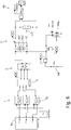
- Figure 6 shows a model of the power train of Figure 5 for simulation to show the benefits of the new type of pre-charge circuit 11.
- the model includes a 3-phase power supply 1a, 3-phase contactors 1b, input current measurement 1c, 6-pulse rectifier 2, and a model of pre-charge circuit 11 with DC-link inductor 12 with the pre-charge winding 121, DC-link capacitance 111 and a power supply circuit 14 to drive the secondary pre-charge winding 122 of the DC-link inductor 12.
- the contactors 1b are present in the model to simulate the in-rush situation where the 3-phase voltages are suddenly applied to the power circuit. In the simulation, the voltage across the DC-link capacitor is measured at oscilloscope 60.
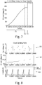
- Figure 7 demonstrates the pre-charge operation by showing the measurement of the DC-link voltage measured across the DC-Link capacitor 111 over time.
- the AC power supply 1a is disconnected via the contactors 1b and the DC-link capacitor 111 is gradually charged in a pre-charge operation over time period 71 via the power supply 14 and coupled DC- link inductor 122.
- time 72 for example, 0.35s
- the DC-link capacitor 111 is almost fully charged to the anticipated level, for example the anticipated level may be 270V.
- the power supply 14 is disabled and the DC-link voltage across capacitor 111 stabilises.
- the 3-phase contactors may be closed, thereby connecting the main power supply 1 to the DC-link. The system is then ready for full power operation.
- FIG. 8 More simulation details are shown in Figure 8 where the time-axis is expanded during the pre-charge operation 71.
- Graph 81 shows the voltage measured across the secondary pre-charge winding 122. Each pulse demonstrates the cycle-by-cycle operation of the switching power supply that drives the pre-charge secondary winding 122.
- Graph 82 shows the DC-link voltage across the DC-link capacitor 111, which shows the voltage increasing by small amounts for each switching event.
- Graph 83 shows the current in the secondary pre-charge winding 122 and the current in the primary DC-link circuit 11.
- the power supply 14 together with controlled switch 14a behaves as a fly-back circuit where energy is stored in the secondary pre-charge winding 122 during the on-period of the power supply MOSFET 14a and is transferred to the DC-link capacitor 111 via the primary winding 121 when the MOSFET 14a is turned off.
Landscapes
- Engineering & Computer Science (AREA)
- Power Engineering (AREA)
- Dc-Dc Converters (AREA)
Abstract
Description
- The examples described herein relate to the field of power conversion.
- The vast majority of power conversion circuits and motor drive controllers are formed with voltage-source converters with large energy storage capacitors decoupling the power input and the converter output. When these circuits are connected to a power source, a large in-rush current flows into the capacitor.
- Such a large inrush current can cause damage to circuits and cause protective circuit breakers to operate. Further, many known solutions typically use a resistor to limit the inrush current, and a parallel shorting switch to short the resistor for normal operation. However, such switches can result in large power losses during normal use.
- It would therefore be desirable to provide a simple apparatus and method to limit the inrush current to controlled levels, whilst reducing power losses during normal operation.
- A power train is described herein comprising a load, a first power supply for providing power to the load; a DC-link capacitor connected to the load; a main converter configured to convert DC power to AC power for powering the load; and pre-charge circuitry comprising pre-charge means configured to, during a first, pre-charge phase, prevent said power from being provided to said load but provide power to said DC-link capacitor to charge said DC-link capacitor, and, further configured to, during a second, post-charge phase, allow said power to be provided from said first power supply to said load.
- In any of the examples described herein, the DC-link capacitor may be connected in parallel with the load.
- In any of the examples described herein, the power train may further comprise a rectifier unit configured to convert AC power from the first power supply to DC power; and a main converter configured to convert DC power to AC power for powering the load. The DC link Capacitor may be connected between said rectifier unit and the main converter to facilitate proper commutation (switching) in the main converter and/or de-couple the main converter from the rectifier.
- In any of the examples described herein, the converter may be configured to facilitate and/or control the power into load. This power can be of a DC or AC nature. In the case of AC, power can be supplied to the load by a single or any polyphase system.
- In any of the examples described herein, the pre-charge circuitry may further comprise a power converter, a second power supply and said pre-charge means may comprise a transformer.
- In any of the examples described herein, the transformer may comprise an inductor connected in series with the first power supply and the DC-link capacitor.
- In any of the examples described herein, the inductor may comprise a primary winding of the transformer.
- In any of the examples described herein, the transformer may further comprise a secondary winding electrically connected to the power converter and the power supply.
- In any of the examples described herein, the power train may further comprise a rectifier unit configured to convert AC power from said first power means to DC power.
- In any of the examples described herein, the power train may further comprise a diode connected in parallel with the DC-link capacitor.
- A method of providing power to a load is also described herein comprising connecting a first power supply to the load, connecting a DC-link capacitor to the load and providing pre-charge circuitry. The pre-charge circuitry may comprise pre-charge means configured to, during a first, pre-charge phase, prevent said power from being provided to said load but provide power to said DC-link capacitor to charge said DC-link capacitor, and, further configured to, during a second, post-charge phase, allow said power to be provided from said first power supply to said load.
- In any of the examples described herein, the step of connecting said DC-link capacitor to said load may comprise connecting said DC-link capacitor in parallel with the load.
- In any of the examples described herein, the method may further comprise providing, in said pre-charge circuitry, a power converter, a second power supply and the pre-charge means may comprises a transformer.
- In any of the examples described herein, the transformer may comprise an inductor and the method may further comprise connecting said inductor in series with the first power supply and the DC-link capacitor.
- In any of the examples described herein, the transformer may comprise a primary winding and a secondary winding and the inductor may be the primary winding of the transformer. The secondary winding may be electrically connected to the power converter and the power supply. The method may further comprise inducing power in the inductor by providing said power to said secondary winding, wherein the induced power charges said DC-link capacitor.
- In any of the examples described herein, the inductor and the DC-link capacitor may act as a filter section.
- In any of the examples described herein, the step of pre-charging the DC-link capacitor may comprise charging the DC-link capacitor to a first, desired voltage level.
- For example, in some examples, said first, desired voltage level may be 240Vdc, although the examples are not limited to this.
-
-
Figure 1 shows a typical power train that may be used in aircraft. -
Figure 2 shows a known use of a parallel boost converter in pre-charge circuitry. -
Figure 3 shows a known use of series buck converter in pre-charge circuitry. -
Figure 4 shows a known use of capacitive voltage dividers in pre-charge circuitry. -
Figure 5 shows a circuit providing improved pre-charge operation and more efficient steady state operation according to the new examples described herein. -
Figure 6 shows a simulated model of the power train ofFigure 5 . -
Figure 7 shows the pre-charge operation of the model ofFigure 6 . -
Figure 8 shows more details of the pre-charge operation shown inFigure 7 . - Whilst the examples discussed herein will be described mainly with reference to their use with a power train found in an aircraft, it is envisaged that the apparatuses and methods described herein could also be utilised in other power trains, or power conversion circuits and are not limited to those found in aircraft.
- Typically, DC-AC conversion circuits include inductive components for EMI filtering and power quality performance.
- A typical, known, power train that may be used in aircraft is presented in
Figure 1 . It consists of agenerator 1, arectifier unit 2, apre-charge circuitry 3, afilter section 4, aconverter 5, and aload 6. The pre-charge functionality of thecircuitry 3 is required to limit the initial in-rush current which shares capacitors infilter section 4. These limits of initial inrush current are defined by aerospace standard or individual customer requirements. - As can be seen in
Figure 1 , a typical example of a knownpre-charge circuitry 3 consists of a power electronics switch 3a connected in parallel with aresistor 3b. During the initial in-rush current that occurs when the 3-phase voltage from thegenerator 1 is applied to the power circuit, switch 3a remains open which causes the current flowing through the DC link capacitor to be limited by theresistor 3b. When the pre-charge is completed, switch 3a is closed, thereby bypassingresistor 3b. Typically thyristor or MOSFET switches are used as the switching device. - However, by utilising such a switch, some of the energy flowing from generator to the load is dissipated in the switch 3a as heat due to a conduction loss. Due to this energy loss, such systems do not support a high efficiency operation of the power train for More/All Electric Aircraft system.
- Alternative approaches to pre-charge
circuitry 3 have been considered. For example, one such approach may be seen inFigure 2 which shows the use of a parallel boost converter. In this case, an output of the boost converter 7 is connected in parallel with the DC link capacitor, with the boost converter 7 being charged from the low voltage source 8 (for example, a battery). - Whilst utilising a boost converter, no power is dissipated in a power electronics switch during normal operation of the power train, as there is no switch. However, such circuits require the need to introduce an auxiliary inductance to support the boost operation. This inductance can be of a significant size, particularly when pre-charge phase has to be kept in hundreds or tens of microseconds time frame.
- Another known approach requires series buck converters, as seen in
Figure 3 . In this case, abuck converter 9 is connected in series with a DC link capacitor whilst thepower electronics switch 10 remains open. In principle, the input voltage applied to thebuck converter 9 is stepped down and then raised up to manage capacitor charging current. However, such an approach again suffers from conduction losses through the power electronics switch 10. - Pre-charge circuits based on capacitive voltage dividers have also been utilised, as seen in
Figure 4 . In principle, they are very similar to buck converter based pre-charge circuits, although they offer a safe power train disconnect in case of a fault. As can be seen inFigure 4 ,capacitive voltage dividers 9a are connected in series with DC link capacitor and bypassed with power electronics switch 10 when the pre-charge phase is finished. However, these again suffer from an efficiency loss due powerelectronic switch 10 caused by conduction losses. - As described above, some existing solutions typically use a resistor to limit the inrush current and a parallel shorting switch (thyristor or MOSFET). Following the pre-charge operation, the shorting switch is turned on, shorting the resistor for normal operation. In contrast to this, the new types of devices and methods described herein eliminate the power losses of the parallel switch, thereby improving circuit efficiency and reducing heat sink mass. They also make use of existing magnetic components for reduced complexity.
- The new examples described herein modify this existing inductive element with a secondary winding to form a transformer. The primary winding is connected as in known devices so that in normal operation the inductor performs its primary filtering function. The secondary winding is connected to a small power converter that can be operated from an auxiliary supply.
- At start-up, the secondary winding is excited with the small power converter to gradually charge the DC link capacitor. Once charged, the small converter is disabled, high voltage can be connected to the main circuit and normal operation commences, preventing a damaging inrush current.
- A new type of device that is capable of providing improved pre-charge operation and more efficient steady state operation is described below and shown in
Figure 5 . As can be seen in this figure, a power train may be provided comprising agenerator 1, arectifier unit 2,pre-charge circuitry 11, aconverter 5, and aload 6.Pre-charge circuitry 11 may comprise a transformer 12 (comprising a primary winding 121 and a secondary winding 122), apower converter 13 and apower supply 14. Further, in some examples, thepre-charge circuitry 11 may optionally comprise adiode 15, if the power train is powered from a DC source. - As can be seen in this figure, the primary winding 121 of
transformer 12 is connected in series with the power supply and theDC link capacitor 111. After pre-charge, this primary winding 121 is visible to the power train as an inductance, and thereby assures compliance with power quality requirements. In this manner, the series connection of primary winding 121 andDC link capacitor 111 may act as a filter section. - The secondary winding 122 is connected to the
power converter 13 and is powered from thepower supply 14. During the pre-charge phase, thepower converter 13 induces flux in thetransformer 12 such that the EMF primary winding 121 closes the pre-charge circuit viaDC link capacitor 111 anddiode 15. In this way, the current flowing through thepre-charge circuit 11 charges theDC link capacitor 111. - The
DC link capacitor 111 may comprise a plurality of conductors connected in parallel, and/or a plurality of capacitors connected in series. A plurality of capacitors in series may be utilised when amultilevel converter 5 is used. - By way of example, when a six
pulse rectifier unit 2 is used, the pre-charge circuit may be closed byrectifier unit 2, or in the case of a DC fed power train, the pre-charge circuit via adedicated diode 15. - Advantageously,
pre-charge circuit 11 does not require extra magnetic components. In this way, an existing DC link inductor may be utilised as a primary winding 121 for thetransformer 12. Further, thepre-charge circuit 11 does not require the use of a power electronic switch. In addition to this, one of the sources of conduction loss in a typical power train is removed, thereby improving efficiency. -
Figure 6 shows a model of the power train ofFigure 5 for simulation to show the benefits of the new type ofpre-charge circuit 11. The model includes a 3-phase power supply 1a, 3-phase contactors 1b, input current measurement 1c, 6-pulse rectifier 2, and a model ofpre-charge circuit 11 with DC-link inductor 12 with the pre-charge winding 121, DC-link capacitance 111 and apower supply circuit 14 to drive the secondary pre-charge winding 122 of the DC-link inductor 12. Thecontactors 1b are present in the model to simulate the in-rush situation where the 3-phase voltages are suddenly applied to the power circuit. In the simulation, the voltage across the DC-link capacitor is measured atoscilloscope 60. -
Figure 7 demonstrates the pre-charge operation by showing the measurement of the DC-link voltage measured across the DC-Link capacitor 111 over time. Initially, theAC power supply 1a is disconnected via thecontactors 1b and the DC-link capacitor 111 is gradually charged in a pre-charge operation overtime period 71 via thepower supply 14 and coupled DC-link inductor 122. At time 72 (for example, 0.35s) the DC-link capacitor 111 is almost fully charged to the anticipated level, for example the anticipated level may be 270V. At this point,point 72, thepower supply 14 is disabled and the DC-link voltage acrosscapacitor 111 stabilises. Atpoint 73, for example when time = 0.4s after pre-charge has begun, the 3-phase contactors may be closed, thereby connecting themain power supply 1 to the DC-link. The system is then ready for full power operation. - If there is a disparity between the level to which the DC-
link capacitor 111 has been charged, and the voltage supplied by themain power supply 1, there may be a secondary in-rush event at the instant when the contactors are closed, i.e. time 73 (for example, when time = 0.4s) since the DC-link capacitor 111 has not reached the final value of charge. In the example ofFigure 7 , DC-link capacitor is precharged to around 240Vdc, whilst the main power supply is provided at 270V. Therefore, when themain power supply 1 is connected in the example ofFigure 7 , then a secondary in-rush charges the DC-link capacitor from 240V to 270V almost instantaneously. Such a secondary in-rush attime 73 may also be seen with traditional pre-charge schemes and hence does not cause any adverse effects or power quality non-compliances. - More simulation details are shown in
Figure 8 where the time-axis is expanded during thepre-charge operation 71.Graph 81 shows the voltage measured across the secondary pre-charge winding 122. Each pulse demonstrates the cycle-by-cycle operation of the switching power supply that drives the pre-charge secondary winding 122.Graph 82 shows the DC-link voltage across the DC-link capacitor 111, which shows the voltage increasing by small amounts for each switching event. Finally,Graph 83 shows the current in the secondary pre-charge winding 122 and the current in the primary DC-link circuit 11. In this simulation, thepower supply 14 together with controlledswitch 14a behaves as a fly-back circuit where energy is stored in the secondary pre-charge winding 122 during the on-period of thepower supply MOSFET 14a and is transferred to the DC-link capacitor 111 via the primary winding 121 when theMOSFET 14a is turned off. - Although this disclosure has been described in terms of preferred examples, it should be understood that these examples are illustrative only and that the claims are not limited to those examples. Those skilled in the art will be able to make modifications and alternatives in view of the disclosure which are contemplated as falling within the scope of the appended claims.
Claims (15)
- A power train, the power train comprising:a load (6);a first power supply (1) for providing power to the load (6);a DC-link capacitor (111) connected to the load (6);a main converter (5) configured to convert DC power to AC power for powering the load (6); andpre-charge circuitry (11) comprising pre-charge means configured to, during a first, pre-charge phase, prevent said power from being provided to said load (6) but provide power to said DC-link capacitor (111) to charge said DC-link capacitor (111), and, further configured to, during a second, post-charge phase, allow said power to be provided from said first power supply (1) to said load (6).
- The power train of claim 1 further comprising
a rectifier unit (2) configured to convert AC power from the first power supply (1) to DC power; and wherein
said DC link capacitor (111) is connected between the rectifier unit (2) and the main converter (5). - The power train of claim 1 or 2 wherein the DC link capacitor (111) comprises a plurality of capacitors connected in parallel to each other and/or a plurality of capacitors connected in series.
- The power train of any preceding claim wherein the pre-charge circuitry (11) further comprises:a power converter (13),a second power supply (14) andwherein said pre-charge means comprises a transformer (12).
- The power train of claim 4 wherein said transformer (12) comprises:
an inductor (121) connected in series with the first power supply (1) and the DC-link capacitor (111). - The power train of claim 5 wherein said inductor comprises:
a primary winding (121) of said transformer (12). - The power train of claim 5 wherein said transformer (12) further comprises
a secondary winding (122) electrically connected to the power converter (13) and the power supply (14). - The power train of any preceding claim, further comprising a diode (15) connected in parallel with the DC-link capacitor (111).
- A method of providing power to a load (6) comprising:connecting a first power supply (1) to the load (6);connecting a DC-link capacitor (111) to a main converter (5);connecting the main converter (5) to the load (6) and providing pre-charge circuitry (11) comprising pre-charge means configured to, during a first, pre-charge phase, prevent said power from being provided to said load (6) but provide power to said DC-link capacitor (111) to charge said DC-link capacitor (111), and, further configured to, during a second, post-charge phase, allow said power to be provided from said first power supply (1) to said load (6).
- The method of claim 9 further comprising
wherein said step of connecting said DC-link capacitor (111) to said load comprises connecting said DC-link capacitor (111) to the converter (5) and connecting the converter (5) to the load (6). - The method of claim 9 or 10 further comprising, providing, in said pre-charge circuitry (11):a power converter (13),a second power supply (14) andwherein said pre-charge means comprises a transformer (12).
- The method of claim 11 wherein said transformer (12) comprises:
an inductor (121) and the method further comprises connecting said inductor (121) in series with the first power supply (1) and the DC-link capacitor (111). - The method of claim 12 wherein said inductor comprises:a primary winding (121) of said transformer (12) anda secondary winding (122) electrically connected to the power converter (13) and the power supply (14), and wherein the method further comprises inducing power in the inductor (121) by providing said power to said secondary winding (122), wherein the induced power charges said DC-link capacitor (111).
- The method of claim 12 to 13, wherein the inductor (121) and the DC-link capacitor (111) act as a filter section.
- The method of any of claims 9 to 14, wherein the step of pre-charging the DC-link capacitor (111) comprises:
charging the DC-link capacitor to a first voltage level.
Priority Applications (2)
| Application Number | Priority Date | Filing Date | Title |
|---|---|---|---|
| EP19275087.5A EP3772810B1 (en) | 2019-08-05 | 2019-08-05 | Dc link capacitor pre-charge method utilizing series boost converter |
| US16/706,354 US11201539B2 (en) | 2019-08-05 | 2019-12-06 | DC link capacitor pre-charge method utilizing series boost converter |
Applications Claiming Priority (1)
| Application Number | Priority Date | Filing Date | Title |
|---|---|---|---|
| EP19275087.5A EP3772810B1 (en) | 2019-08-05 | 2019-08-05 | Dc link capacitor pre-charge method utilizing series boost converter |
Publications (2)
| Publication Number | Publication Date |
|---|---|
| EP3772810A1 true EP3772810A1 (en) | 2021-02-10 |
| EP3772810B1 EP3772810B1 (en) | 2022-03-02 |
Family
ID=67551304
Family Applications (1)
| Application Number | Title | Priority Date | Filing Date |
|---|---|---|---|
| EP19275087.5A Active EP3772810B1 (en) | 2019-08-05 | 2019-08-05 | Dc link capacitor pre-charge method utilizing series boost converter |
Country Status (2)
| Country | Link |
|---|---|
| US (1) | US11201539B2 (en) |
| EP (1) | EP3772810B1 (en) |
Cited By (1)
| Publication number | Priority date | Publication date | Assignee | Title |
|---|---|---|---|---|
| EP4671036A1 (en) * | 2024-06-26 | 2025-12-31 | Valeo eAutomotive Germany GmbH | ON-BOARD CHARGING SWITCH, ON-BOARD CHARGING DEVICE, ON-BOARD CHARGING SYSTEM AND VEHICLE |
Families Citing this family (2)
| Publication number | Priority date | Publication date | Assignee | Title |
|---|---|---|---|---|
| DE102023105095A1 (en) * | 2023-03-01 | 2024-09-05 | TRUMPF Hüttinger GmbH + Co. KG | Circuit arrangement and a method for operating a circuit arrangement |
| US20250239848A1 (en) * | 2024-01-19 | 2025-07-24 | Honeywell International Inc. | Inrush protection circuit for redundant power supply |
Citations (2)
| Publication number | Priority date | Publication date | Assignee | Title |
|---|---|---|---|---|
| US20030002298A1 (en) * | 2000-11-30 | 2003-01-02 | Hussein Khalid Hassan | Power conversion device |
| WO2019021128A1 (en) * | 2017-07-25 | 2019-01-31 | Quepal Limited | A load dump |
Family Cites Families (6)
| Publication number | Priority date | Publication date | Assignee | Title |
|---|---|---|---|---|
| US7742317B2 (en) * | 2007-12-19 | 2010-06-22 | Gm Global Technology Operations, Inc. | Precharging boost converters in DC to DC power converters |
| JP5120550B2 (en) * | 2008-03-19 | 2013-01-16 | 本田技研工業株式会社 | Power converter |
| US7965529B2 (en) | 2008-05-13 | 2011-06-21 | Eaton Corporation | Voltage source inverter and medium voltage pre-charge circuit therefor |
| GB2560195B (en) | 2017-03-03 | 2020-01-08 | Ge Energy Power Conversion Technology Ltd | Electric circuits and power systems incorporating the same |
| US20180331569A1 (en) | 2017-05-15 | 2018-11-15 | Vertiv Srl | Technique For Lowering Inrush Current To An Uninterruptible Power Supply With A Transformer |
| DE102017127311A1 (en) | 2017-11-20 | 2019-05-23 | Ge Energy Power Conversion Technology Limited | Apparatus and method for biasing a power transformer in a power converter system |
-
2019
- 2019-08-05 EP EP19275087.5A patent/EP3772810B1/en active Active
- 2019-12-06 US US16/706,354 patent/US11201539B2/en active Active
Patent Citations (2)
| Publication number | Priority date | Publication date | Assignee | Title |
|---|---|---|---|---|
| US20030002298A1 (en) * | 2000-11-30 | 2003-01-02 | Hussein Khalid Hassan | Power conversion device |
| WO2019021128A1 (en) * | 2017-07-25 | 2019-01-31 | Quepal Limited | A load dump |
Cited By (1)
| Publication number | Priority date | Publication date | Assignee | Title |
|---|---|---|---|---|
| EP4671036A1 (en) * | 2024-06-26 | 2025-12-31 | Valeo eAutomotive Germany GmbH | ON-BOARD CHARGING SWITCH, ON-BOARD CHARGING DEVICE, ON-BOARD CHARGING SYSTEM AND VEHICLE |
Also Published As
| Publication number | Publication date |
|---|---|
| EP3772810B1 (en) | 2022-03-02 |
| US11201539B2 (en) | 2021-12-14 |
| US20210044211A1 (en) | 2021-02-11 |
Similar Documents
| Publication | Publication Date | Title |
|---|---|---|
| US20200006970A1 (en) | Power conversion system and method for pre-charging dc-bus capacitors therein | |
| US11496053B2 (en) | Power conversion system with dc-bus pre-charge | |
| CN102742140B (en) | Power inverter with multi-fed onboard power supply | |
| US10554148B2 (en) | Device and method for premagnetization of a power transformer in a converter system | |
| US8476859B2 (en) | DC power for SGCT devices using a high frequency current loop with multiple current transformers | |
| US20110038185A1 (en) | Low stress soft charge circuit for diode front end variable frequency drive | |
| CN108463935A (en) | Two-way DC/DC converters and the method to charge from low-voltage battery to the intermediate circuit capacitor of DC/DC converters | |
| Liu et al. | High step-up Y-source inverter with reduced DC-link voltage spikes | |
| TWI473376B (en) | Power supply system and control method thereof | |
| US20150155791A1 (en) | Power supply apparatus and method of generating power by the same | |
| US11201539B2 (en) | DC link capacitor pre-charge method utilizing series boost converter | |
| CN114552959A (en) | Auxiliary pre-charging device and method for power converter and power converter | |
| CN115693875A (en) | Charger capable of bidirectional power transmission | |
| US20200121939A1 (en) | Method and device for defibrillation | |
| Ma et al. | Overview of 100-kV/60-A high-voltage power supply utilized for the ECRH system on J-TEXT tokamak | |
| CN114175481A (en) | DC-DC converter of power conversion system | |
| CA2853556C (en) | Double-rectifier for a multi-phase contactless energy transmission system | |
| JP2002354830A (en) | High voltage inverter device | |
| US20150249400A1 (en) | Converter | |
| US9673741B2 (en) | System for supplying electrical power to a load and corresponding power supply method | |
| WO2011115827A2 (en) | Method and system delivering a controlled voltage | |
| JP2002345258A (en) | Inverter device | |
| CN115244841A (en) | Start-up system for cascaded modular power converters | |
| CN111669047A (en) | Power Units and Power Systems | |
| Kulkarni et al. | New start-up scheme for HF transformer link photovoltaic inverter |
Legal Events
| Date | Code | Title | Description |
|---|---|---|---|
| PUAI | Public reference made under article 153(3) epc to a published international application that has entered the european phase |
Free format text: ORIGINAL CODE: 0009012 |
|
| STAA | Information on the status of an ep patent application or granted ep patent |
Free format text: STATUS: THE APPLICATION HAS BEEN PUBLISHED |
|
| AK | Designated contracting states |
Kind code of ref document: A1 Designated state(s): AL AT BE BG CH CY CZ DE DK EE ES FI FR GB GR HR HU IE IS IT LI LT LU LV MC MK MT NL NO PL PT RO RS SE SI SK SM TR |
|
| AX | Request for extension of the european patent |
Extension state: BA ME |
|
| STAA | Information on the status of an ep patent application or granted ep patent |
Free format text: STATUS: REQUEST FOR EXAMINATION WAS MADE |
|
| 17P | Request for examination filed |
Effective date: 20210810 |
|
| RBV | Designated contracting states (corrected) |
Designated state(s): AL AT BE BG CH CY CZ DE DK EE ES FI FR GB GR HR HU IE IS IT LI LT LU LV MC MK MT NL NO PL PT RO RS SE SI SK SM TR |
|
| GRAP | Despatch of communication of intention to grant a patent |
Free format text: ORIGINAL CODE: EPIDOSNIGR1 |
|
| STAA | Information on the status of an ep patent application or granted ep patent |
Free format text: STATUS: GRANT OF PATENT IS INTENDED |
|
| RIC1 | Information provided on ipc code assigned before grant |
Ipc: H02M 1/00 20060101ALN20210906BHEP Ipc: H02M 3/335 20060101ALN20210906BHEP Ipc: H02M 7/06 20060101ALI20210906BHEP Ipc: H02M 1/36 20070101ALI20210906BHEP Ipc: H02M 5/458 20060101AFI20210906BHEP |
|
| RIC1 | Information provided on ipc code assigned before grant |
Ipc: H02M 1/00 20060101ALN20210922BHEP Ipc: H02M 3/335 20060101ALN20210922BHEP Ipc: H02M 7/06 20060101ALI20210922BHEP Ipc: H02M 1/36 20070101ALI20210922BHEP Ipc: H02M 5/458 20060101AFI20210922BHEP |
|
| INTG | Intention to grant announced |
Effective date: 20211005 |
|
| RIC1 | Information provided on ipc code assigned before grant |
Ipc: H02M 1/00 20060101ALN20210927BHEP Ipc: H02M 3/335 20060101ALN20210927BHEP Ipc: H02M 7/06 20060101ALI20210927BHEP Ipc: H02M 1/36 20070101ALI20210927BHEP Ipc: H02M 5/458 20060101AFI20210927BHEP |
|
| GRAS | Grant fee paid |
Free format text: ORIGINAL CODE: EPIDOSNIGR3 |
|
| GRAA | (expected) grant |
Free format text: ORIGINAL CODE: 0009210 |
|
| STAA | Information on the status of an ep patent application or granted ep patent |
Free format text: STATUS: THE PATENT HAS BEEN GRANTED |
|
| AK | Designated contracting states |
Kind code of ref document: B1 Designated state(s): AL AT BE BG CH CY CZ DE DK EE ES FI FR GB GR HR HU IE IS IT LI LT LU LV MC MK MT NL NO PL PT RO RS SE SI SK SM TR |
|
| REG | Reference to a national code |
Ref country code: GB Ref legal event code: FG4D |
|
| REG | Reference to a national code |
Ref country code: CH Ref legal event code: EP Ref country code: AT Ref legal event code: REF Ref document number: 1473075 Country of ref document: AT Kind code of ref document: T Effective date: 20220315 |
|
| REG | Reference to a national code |
Ref country code: DE Ref legal event code: R096 Ref document number: 602019012104 Country of ref document: DE |
|
| REG | Reference to a national code |
Ref country code: IE Ref legal event code: FG4D |
|
| REG | Reference to a national code |
Ref country code: LT Ref legal event code: MG9D |
|
| REG | Reference to a national code |
Ref country code: NL Ref legal event code: MP Effective date: 20220302 |
|
| PG25 | Lapsed in a contracting state [announced via postgrant information from national office to epo] |
Ref country code: SE Free format text: LAPSE BECAUSE OF FAILURE TO SUBMIT A TRANSLATION OF THE DESCRIPTION OR TO PAY THE FEE WITHIN THE PRESCRIBED TIME-LIMIT Effective date: 20220302 Ref country code: RS Free format text: LAPSE BECAUSE OF FAILURE TO SUBMIT A TRANSLATION OF THE DESCRIPTION OR TO PAY THE FEE WITHIN THE PRESCRIBED TIME-LIMIT Effective date: 20220302 Ref country code: NO Free format text: LAPSE BECAUSE OF FAILURE TO SUBMIT A TRANSLATION OF THE DESCRIPTION OR TO PAY THE FEE WITHIN THE PRESCRIBED TIME-LIMIT Effective date: 20220602 Ref country code: LT Free format text: LAPSE BECAUSE OF FAILURE TO SUBMIT A TRANSLATION OF THE DESCRIPTION OR TO PAY THE FEE WITHIN THE PRESCRIBED TIME-LIMIT Effective date: 20220302 Ref country code: HR Free format text: LAPSE BECAUSE OF FAILURE TO SUBMIT A TRANSLATION OF THE DESCRIPTION OR TO PAY THE FEE WITHIN THE PRESCRIBED TIME-LIMIT Effective date: 20220302 Ref country code: ES Free format text: LAPSE BECAUSE OF FAILURE TO SUBMIT A TRANSLATION OF THE DESCRIPTION OR TO PAY THE FEE WITHIN THE PRESCRIBED TIME-LIMIT Effective date: 20220302 Ref country code: BG Free format text: LAPSE BECAUSE OF FAILURE TO SUBMIT A TRANSLATION OF THE DESCRIPTION OR TO PAY THE FEE WITHIN THE PRESCRIBED TIME-LIMIT Effective date: 20220602 |
|
| REG | Reference to a national code |
Ref country code: AT Ref legal event code: MK05 Ref document number: 1473075 Country of ref document: AT Kind code of ref document: T Effective date: 20220302 |
|
| PG25 | Lapsed in a contracting state [announced via postgrant information from national office to epo] |
Ref country code: PL Free format text: LAPSE BECAUSE OF FAILURE TO SUBMIT A TRANSLATION OF THE DESCRIPTION OR TO PAY THE FEE WITHIN THE PRESCRIBED TIME-LIMIT Effective date: 20220302 Ref country code: LV Free format text: LAPSE BECAUSE OF FAILURE TO SUBMIT A TRANSLATION OF THE DESCRIPTION OR TO PAY THE FEE WITHIN THE PRESCRIBED TIME-LIMIT Effective date: 20220302 Ref country code: GR Free format text: LAPSE BECAUSE OF FAILURE TO SUBMIT A TRANSLATION OF THE DESCRIPTION OR TO PAY THE FEE WITHIN THE PRESCRIBED TIME-LIMIT Effective date: 20220603 Ref country code: FI Free format text: LAPSE BECAUSE OF FAILURE TO SUBMIT A TRANSLATION OF THE DESCRIPTION OR TO PAY THE FEE WITHIN THE PRESCRIBED TIME-LIMIT Effective date: 20220302 |
|
| PG25 | Lapsed in a contracting state [announced via postgrant information from national office to epo] |
Ref country code: NL Free format text: LAPSE BECAUSE OF FAILURE TO SUBMIT A TRANSLATION OF THE DESCRIPTION OR TO PAY THE FEE WITHIN THE PRESCRIBED TIME-LIMIT Effective date: 20220302 |
|
| PG25 | Lapsed in a contracting state [announced via postgrant information from national office to epo] |
Ref country code: SM Free format text: LAPSE BECAUSE OF FAILURE TO SUBMIT A TRANSLATION OF THE DESCRIPTION OR TO PAY THE FEE WITHIN THE PRESCRIBED TIME-LIMIT Effective date: 20220302 Ref country code: SK Free format text: LAPSE BECAUSE OF FAILURE TO SUBMIT A TRANSLATION OF THE DESCRIPTION OR TO PAY THE FEE WITHIN THE PRESCRIBED TIME-LIMIT Effective date: 20220302 Ref country code: RO Free format text: LAPSE BECAUSE OF FAILURE TO SUBMIT A TRANSLATION OF THE DESCRIPTION OR TO PAY THE FEE WITHIN THE PRESCRIBED TIME-LIMIT Effective date: 20220302 Ref country code: PT Free format text: LAPSE BECAUSE OF FAILURE TO SUBMIT A TRANSLATION OF THE DESCRIPTION OR TO PAY THE FEE WITHIN THE PRESCRIBED TIME-LIMIT Effective date: 20220704 Ref country code: EE Free format text: LAPSE BECAUSE OF FAILURE TO SUBMIT A TRANSLATION OF THE DESCRIPTION OR TO PAY THE FEE WITHIN THE PRESCRIBED TIME-LIMIT Effective date: 20220302 Ref country code: CZ Free format text: LAPSE BECAUSE OF FAILURE TO SUBMIT A TRANSLATION OF THE DESCRIPTION OR TO PAY THE FEE WITHIN THE PRESCRIBED TIME-LIMIT Effective date: 20220302 Ref country code: AT Free format text: LAPSE BECAUSE OF FAILURE TO SUBMIT A TRANSLATION OF THE DESCRIPTION OR TO PAY THE FEE WITHIN THE PRESCRIBED TIME-LIMIT Effective date: 20220302 |
|
| PG25 | Lapsed in a contracting state [announced via postgrant information from national office to epo] |
Ref country code: IS Free format text: LAPSE BECAUSE OF FAILURE TO SUBMIT A TRANSLATION OF THE DESCRIPTION OR TO PAY THE FEE WITHIN THE PRESCRIBED TIME-LIMIT Effective date: 20220702 Ref country code: AL Free format text: LAPSE BECAUSE OF FAILURE TO SUBMIT A TRANSLATION OF THE DESCRIPTION OR TO PAY THE FEE WITHIN THE PRESCRIBED TIME-LIMIT Effective date: 20220302 |
|
| REG | Reference to a national code |
Ref country code: DE Ref legal event code: R097 Ref document number: 602019012104 Country of ref document: DE |
|
| PLBE | No opposition filed within time limit |
Free format text: ORIGINAL CODE: 0009261 |
|
| STAA | Information on the status of an ep patent application or granted ep patent |
Free format text: STATUS: NO OPPOSITION FILED WITHIN TIME LIMIT |
|
| PG25 | Lapsed in a contracting state [announced via postgrant information from national office to epo] |
Ref country code: DK Free format text: LAPSE BECAUSE OF FAILURE TO SUBMIT A TRANSLATION OF THE DESCRIPTION OR TO PAY THE FEE WITHIN THE PRESCRIBED TIME-LIMIT Effective date: 20220302 |
|
| 26N | No opposition filed |
Effective date: 20221205 |
|
| PG25 | Lapsed in a contracting state [announced via postgrant information from national office to epo] |
Ref country code: SI Free format text: LAPSE BECAUSE OF FAILURE TO SUBMIT A TRANSLATION OF THE DESCRIPTION OR TO PAY THE FEE WITHIN THE PRESCRIBED TIME-LIMIT Effective date: 20220302 |
|
| PG25 | Lapsed in a contracting state [announced via postgrant information from national office to epo] |
Ref country code: MC Free format text: LAPSE BECAUSE OF FAILURE TO SUBMIT A TRANSLATION OF THE DESCRIPTION OR TO PAY THE FEE WITHIN THE PRESCRIBED TIME-LIMIT Effective date: 20220302 |
|
| REG | Reference to a national code |
Ref country code: CH Ref legal event code: PL |
|
| PG25 | Lapsed in a contracting state [announced via postgrant information from national office to epo] |
Ref country code: LU Free format text: LAPSE BECAUSE OF NON-PAYMENT OF DUE FEES Effective date: 20220805 Ref country code: LI Free format text: LAPSE BECAUSE OF NON-PAYMENT OF DUE FEES Effective date: 20220831 Ref country code: CH Free format text: LAPSE BECAUSE OF NON-PAYMENT OF DUE FEES Effective date: 20220831 |
|
| REG | Reference to a national code |
Ref country code: BE Ref legal event code: MM Effective date: 20220831 |
|
| P01 | Opt-out of the competence of the unified patent court (upc) registered |
Effective date: 20230603 |
|
| PG25 | Lapsed in a contracting state [announced via postgrant information from national office to epo] |
Ref country code: IT Free format text: LAPSE BECAUSE OF FAILURE TO SUBMIT A TRANSLATION OF THE DESCRIPTION OR TO PAY THE FEE WITHIN THE PRESCRIBED TIME-LIMIT Effective date: 20220302 Ref country code: IE Free format text: LAPSE BECAUSE OF NON-PAYMENT OF DUE FEES Effective date: 20220805 |
|
| PG25 | Lapsed in a contracting state [announced via postgrant information from national office to epo] |
Ref country code: BE Free format text: LAPSE BECAUSE OF NON-PAYMENT OF DUE FEES Effective date: 20220831 |
|
| PG25 | Lapsed in a contracting state [announced via postgrant information from national office to epo] |
Ref country code: CY Free format text: LAPSE BECAUSE OF FAILURE TO SUBMIT A TRANSLATION OF THE DESCRIPTION OR TO PAY THE FEE WITHIN THE PRESCRIBED TIME-LIMIT Effective date: 20220302 |
|
| PG25 | Lapsed in a contracting state [announced via postgrant information from national office to epo] |
Ref country code: MK Free format text: LAPSE BECAUSE OF FAILURE TO SUBMIT A TRANSLATION OF THE DESCRIPTION OR TO PAY THE FEE WITHIN THE PRESCRIBED TIME-LIMIT Effective date: 20220302 Ref country code: HU Free format text: LAPSE BECAUSE OF FAILURE TO SUBMIT A TRANSLATION OF THE DESCRIPTION OR TO PAY THE FEE WITHIN THE PRESCRIBED TIME-LIMIT; INVALID AB INITIO Effective date: 20190805 |
|
| PG25 | Lapsed in a contracting state [announced via postgrant information from national office to epo] |
Ref country code: MT Free format text: LAPSE BECAUSE OF FAILURE TO SUBMIT A TRANSLATION OF THE DESCRIPTION OR TO PAY THE FEE WITHIN THE PRESCRIBED TIME-LIMIT Effective date: 20220302 |
|
| PGFP | Annual fee paid to national office [announced via postgrant information from national office to epo] |
Ref country code: DE Payment date: 20250724 Year of fee payment: 7 |
|
| PGFP | Annual fee paid to national office [announced via postgrant information from national office to epo] |
Ref country code: GB Payment date: 20250724 Year of fee payment: 7 |
|
| PGFP | Annual fee paid to national office [announced via postgrant information from national office to epo] |
Ref country code: FR Payment date: 20250725 Year of fee payment: 7 |
|
| PG25 | Lapsed in a contracting state [announced via postgrant information from national office to epo] |
Ref country code: TR Free format text: LAPSE BECAUSE OF FAILURE TO SUBMIT A TRANSLATION OF THE DESCRIPTION OR TO PAY THE FEE WITHIN THE PRESCRIBED TIME-LIMIT Effective date: 20220302 |