EP3772216A1 - Dispositif de commande de sortie, dispositif de sortie laser, dispositif d'enregistrement d'images, procédé de commande de sortie et programme de commande de sortie - Google Patents
Dispositif de commande de sortie, dispositif de sortie laser, dispositif d'enregistrement d'images, procédé de commande de sortie et programme de commande de sortie Download PDFInfo
- Publication number
- EP3772216A1 EP3772216A1 EP20188336.0A EP20188336A EP3772216A1 EP 3772216 A1 EP3772216 A1 EP 3772216A1 EP 20188336 A EP20188336 A EP 20188336A EP 3772216 A1 EP3772216 A1 EP 3772216A1
- Authority
- EP
- European Patent Office
- Prior art keywords
- output
- power
- time
- output element
- laser
- Prior art date
- Legal status (The legal status is an assumption and is not a legal conclusion. Google has not performed a legal analysis and makes no representation as to the accuracy of the status listed.)
- Granted
Links
- 238000000034 method Methods 0.000 title claims description 45
- 238000012937 correction Methods 0.000 claims abstract description 98
- 230000003287 optical effect Effects 0.000 claims description 28
- 230000008569 process Effects 0.000 claims description 14
- 230000008878 coupling Effects 0.000 claims description 11
- 238000010168 coupling process Methods 0.000 claims description 11
- 238000005859 coupling reaction Methods 0.000 claims description 11
- 230000008859 change Effects 0.000 claims description 9
- 230000006870 function Effects 0.000 description 65
- 238000010586 diagram Methods 0.000 description 14
- 239000000835 fiber Substances 0.000 description 13
- 238000001816 cooling Methods 0.000 description 9
- 239000000110 cooling liquid Substances 0.000 description 9
- 239000013307 optical fiber Substances 0.000 description 8
- 230000007423 decrease Effects 0.000 description 5
- 238000003860 storage Methods 0.000 description 5
- 230000036962 time dependent Effects 0.000 description 5
- 238000004891 communication Methods 0.000 description 4
- 238000001514 detection method Methods 0.000 description 4
- 230000000694 effects Effects 0.000 description 3
- 239000004020 conductor Substances 0.000 description 2
- 230000007547 defect Effects 0.000 description 2
- 230000006866 deterioration Effects 0.000 description 2
- 238000009434 installation Methods 0.000 description 2
- 230000001678 irradiating effect Effects 0.000 description 2
- 238000004519 manufacturing process Methods 0.000 description 2
- 238000002844 melting Methods 0.000 description 2
- 230000008018 melting Effects 0.000 description 2
- 238000012986 modification Methods 0.000 description 2
- 230000004048 modification Effects 0.000 description 2
- 238000007639 printing Methods 0.000 description 2
- 238000012545 processing Methods 0.000 description 2
- 238000001454 recorded image Methods 0.000 description 2
- 239000004065 semiconductor Substances 0.000 description 2
- 238000012546 transfer Methods 0.000 description 2
- 230000005540 biological transmission Effects 0.000 description 1
- 230000000903 blocking effect Effects 0.000 description 1
- 238000004364 calculation method Methods 0.000 description 1
- 238000006243 chemical reaction Methods 0.000 description 1
- 239000011248 coating agent Substances 0.000 description 1
- 238000000576 coating method Methods 0.000 description 1
- 238000004040 coloring Methods 0.000 description 1
- 238000012888 cubic function Methods 0.000 description 1
- 230000003247 decreasing effect Effects 0.000 description 1
- 230000000593 degrading effect Effects 0.000 description 1
- 238000013461 design Methods 0.000 description 1
- 238000005516 engineering process Methods 0.000 description 1
- 238000009499 grossing Methods 0.000 description 1
- 238000010330 laser marking Methods 0.000 description 1
- 238000007648 laser printing Methods 0.000 description 1
- 238000012886 linear function Methods 0.000 description 1
- 239000007788 liquid Substances 0.000 description 1
- 238000012544 monitoring process Methods 0.000 description 1
- 230000001590 oxidative effect Effects 0.000 description 1
- 238000002360 preparation method Methods 0.000 description 1
- 238000012887 quadratic function Methods 0.000 description 1
- 230000004044 response Effects 0.000 description 1
- 230000000630 rising effect Effects 0.000 description 1
- 239000007787 solid Substances 0.000 description 1
- 238000011144 upstream manufacturing Methods 0.000 description 1
Images


Classifications
-
- H—ELECTRICITY
- H04—ELECTRIC COMMUNICATION TECHNIQUE
- H04N—PICTORIAL COMMUNICATION, e.g. TELEVISION
- H04N1/00—Scanning, transmission or reproduction of documents or the like, e.g. facsimile transmission; Details thereof
- H04N1/00885—Power supply means, e.g. arrangements for the control of power supply to the apparatus or components thereof
-
- H—ELECTRICITY
- H04—ELECTRIC COMMUNICATION TECHNIQUE
- H04N—PICTORIAL COMMUNICATION, e.g. TELEVISION
- H04N1/00—Scanning, transmission or reproduction of documents or the like, e.g. facsimile transmission; Details thereof
- H04N1/23—Reproducing arrangements
Definitions
- the present invention relates to an output control device, a laser output device, an image recording device, an output control method, and an output control program.
- laser devices have been developed to provide an object with state changes such as coloring, melting, and surface modification by thermal energy.
- Such laser devices typically apply laser light emitted by laser emitting elements (laser diodes, VCSELs, or the like) to an object through an optical system.
- laser emitting elements laser diodes, VCSELs, or the like
- the above laser devices employ a switching-type pulse current drive control method to improve efficiency of drive circuits of laser emitting elements.
- a diode load such as a laser diode
- the light output is typically controlled by current drive.
- Patent Document 1 discloses a switching-type pulse current drive control method.
- the disclosed switching-type pulse current drive control method includes chopping an input voltage by a switching element, subsequently feeding back a current flowing through a smoothing element such as a coil, and switching a direction of electric current application according to laser application timing.
- Patent Document 1 Japanese Patent. No. 6077263
- This switching-type pulse current drive control method appears to be problematic because this method may exhibit a large variation in the output due to ripple current.
- an output control device includes at least one output element; and a controller configured to control an output of the at least one output element by switching on and off of a power supply to supply an electric current to the at least one output element, wherein upon a power-on time and a power-off time of the power supply to supply an electric current to the at least one output element being determined according to a desired output of the at least one output element, the controller calculates a power-on time correction value using a correction function individually set for the at least one output element on a per output element basis, and corrects the power-on time and the power-off time, based on the calculated power-on time correction value.
- thermosensitive recording label affixed to a shipping container.
- the shipping container is given as an example of a structure with a thermosensitive recording medium, which acts as a recording target.
- "recording” means printing a logo, a product name, a serial number, a model number, or the like, by irradiating a recording target with light such as a laser to perform surface melting, surface burning, surface peeling, surface oxidizing, surface shaving, or surface decolorating.
- the “recording” may also mean “contactless marking”, “laser marking”, “laser typing”, or “laser printing”.
- FIG. 1 is a schematic perspective diagram illustrating an image recording system 100 acting as an image recording device according to an embodiment.
- an X-axis direction indicates a transport direction of a transport container C
- a Z-axis direction indicates a vertical direction
- a Y-axis direction indicates a direction orthogonal to both the transfer direction and the vertical direction.
- the image recording system 100 is configured to record an image by irradiating a thermosensitive recording label RL affixed to a container C with laser light.
- the container C, to which thermosensitive recording label RL is affixed indicates a recording target.
- the image recording system 100 includes a conveyor device 10 serving as a transport unit configured to transport a recording target, a recording device 14, a system control device 18, a reading device 15, a shielding cover 11, and the like.
- the recording device 14 is configured to irradiate a thermosensitive recording label RL with laser light so as to record an image as a visible image on a recording target.
- the recording device 14 is disposed at a -Y side of the conveyor device 10, i.e., at the -Y side of a conveyor path.
- the shield cover 11 is configured to prevent laser light emitted from the recording device 14 from diffusing by blocking the laser light.
- the shield cover 11 has a black alumite coating on its surface.
- the shield cover 11 is provided with an opening 11a on a side facing the recording device 14 so as to pass laser light through the opening 11a.
- the conveyor device 10 used herein is a roller conveyor; however, the conveyor device 10 may be a belt conveyor.
- the system control device 18 is connected to a conveyor device 10, the recording device 14, the reading device 15, and the like, so as to control the entire image recording system 100. Further, as will be described later, the reading device 15 is configured to read a code image, such as a bar code or a QR code (a registered trademark), recorded on a recording target. The system control device 18 checks whether an image is correctly recorded based on information read by the reading device 15.
- a code image such as a bar code or a QR code (a registered trademark
- FIG. 2 is a schematic perspective diagram illustrating a configuration of the recording device 14 according to an embodiment.
- the recording device 14 is a fiber array recording device.
- the fiber array recording device is configured to record an image by using a fiber array.
- the fiber array is composed of a plurality of optical fiber laser emitting portions, where the plurality of optical fiber laser emitting portions are disposed in a main scanning direction (Z-axis direction) perpendicular to a sub-scanning direction (X-axis direction) of the container C, which acts as a recording target.
- the sub-scanning direction (X-axis direction) is a moving direction of the container C.
- the recording device 14 includes a laser array unit 14a, a fiber array unit 14b, and an optical unit 43.
- the laser array unit 14a includes a plurality of laser emitting elements 41 (output elements) disposed in an array, a cooler unit 50 configured to cool the laser emitting elements 41, a plurality of drivers 45 disposed corresponding to the laser emitting elements 41 for driving the corresponding laser emitting elements 41, and a controller 46 configured to control the plurality of drivers 45.
- a power supply 48 and an image information output unit 47 such as a personal computer are connected to the controller 46.
- the power supply 48 is configured to supply power to the laser emitting elements 41
- the image information output unit 47 is configured to output image information.
- Laser types for the laser emitting elements 41 may be optionally selected according to purpose of applications; examples include a semiconductor laser, a solid-state laser, a dye laser, or the like. Among these, a semiconductor laser may be preferably used for the laser emitting elements 41, in view of wider wavelength selectivity, downsizing of devices due to its small size, and low cost.
- the wavelength of laser light emitted by a laser emitting element 41 is not particularly limited, and may be appropriately selected according to applications. However, the wavelength of laser light emitted by the laser emitting element 41 may preferably be from 700 nm to 2000 nm and more preferably from 780 nm to 1600 nm.
- the laser emitting elements 41 acting as emitting units, not all the energy applied to the laser emitting elements 41 is converted into laser light.
- the energy that is not converted into laser light is converted to heat such that the laser emitting elements 41 generate heat.
- the laser emitting elements 41 are required to be cooled down by the cooler unit 50, which acts as a cooler unit.
- the recording device 14 includes the fiber array unit 14b in order to dispose the laser emitting elements 41 separately from each other. This arrangement reduces thermal effects from the neighboring laser emitting elements 41, thereby efficiently cooling the laser emitting elements 41.
- the output of laser light indicates the average output measured with a power meter.
- the cooler unit 50 is a liquid cooling system that cools the laser emitting elements 41 by circulating cooling liquid.
- the cooler unit 50 includes a heat receiver 51 configured to receive heat from each of the laser emitting elements 41, and a heat sink 52 configured to transfer heat from the cooling liquid.
- the heat receiver 51 and the heat sink 52 are connected via cooling pipes 53a and 53b.
- the heat receiver 51 is provided with the cooling pipes for flowing the cooling liquid.
- the cooling pipes are made of an excellent heat conducting material inside a case, which is also made of an excellent heat conducting material.
- a plurality of laser emitting elements 41 are disposed in an array on the heat receiver 51.
- the heat sink 52 includes a radiator and a pump for circulating a cooling liquid.
- the cooling liquid fed by the pump of the heat sink 52 flows through the cooling pipe 53a into the heat receiver 51. While the cooling liquid moves through the cooling pipe 53a inside the heat receiver 51, the cooling liquid removes heat from the laser emitting elements 41 disposed on the heat receiver 51, thereby cooling the laser emitting elements 41.
- the cooling liquid, which has flown from the heat receiver 51 and removed the heat of the laser emitting elements 41 moves inside the cooling pipe 53b, and flows into the radiator of the heat sink 52, and is then cooled by the radiator.
- the cooling liquid cooled by the radiator is fed back to the heat receiver 51 by the pump.
- the fiber array unit 14b includes a plurality of optical fibers 42 disposed corresponding to the laser emitting elements 41, and an array head 44 configured to hold laser output portions of the optical fibers 42 in an array along a vertical direction (a Z-axis direction).
- the laser input portions of the respective optical fibers 42 are affixed to laser output surfaces of the laser emitting elements 41.
- the image information output unit 47 such as a personal computer (PC), inputs image data to a controller 46.
- the controller 46 generates a drive signal for driving each driver 45 based on the input image data.
- the controller 46 transmits the generated drive signal to the corresponding driver 45.
- the controller 46 includes a clock generator.
- the controller 46 transmits a drive signal to the corresponding driver 45 when the number of clocks generated by the clock generator achieves a predetermined number of clocks.
- the drivers 45 drive respective laser emitting elements 41.
- the laser emitting elements 41 emit laser light according to driving states of the drivers 45.
- Laser light emitted from laser emitting elements 41 enters the respective optical fibers 42, and is then output (emitted) from the laser output portions of the optical fibers 42.
- the laser light emitted from the laser output portions of the optical fibers 42 passes through a collimating lens 43a and a collecting lens 43b of the optical unit 43, and is then applied to a surface of thermosensitive recording label RL of the container C, which acts a recording target.
- An image is recorded on the surface of thermosensitive recording label RL by being heated by the laser light applied on the surface of thermosensitive recording label RL.
- the recording device 14 includes a laser array having a plurality of laser emitting elements 41 disposed in an array. In this configuration, an image can be recorded on a recording target by simply controlling ON/OFF of the laser emitting elements 41 corresponding to respective pixels.
- the recording device 14 according to the present embodiment when used, an image having a large amount of information can be recorded on the recording target without temporarily stopping transportation of the container C.
- the recording device 14 according to the present embodiment needs to record an image having a large amount of information on a recording target, the image can be recorded without degrading productivity.
- FIG. 3 is a block diagram partially illustrating electric circuits of the image recording system 100 according to an embodiment.
- the system control device 18 illustrated in FIG. 3 includes a CPU, a RAM, a ROM, a non-volatile memory, and the like (not illustrated).
- the system control device 18 is configured to control driving of various devices and perform various operations of the image recording system 100.
- the system control device 18 is connected to a conveyor device 10, the recording device 14, a reading device 15, a control panel 181, an image information output unit 47, or the like.
- the control panel 181 includes a touch panel display, and a variety of keys for displaying images or receiving various information input upon an operator's operating keys.
- the system control device 18 functions as an image recorder in response to the CPU being operated according to a program stored in the ROM or the like.
- the system control device 18 is configured to control the recording device 14 to apply a laser to a recording target, which moves relative to the recording device 14 in a direction differing from a predetermined direction.
- the recording target is heated by laser applied to form image dots, thereby recording an image.
- an operator places the container C containing packages on the conveyor device 10.
- the operator places the container C to direct a lateral side of a body of the container C at a -Y side that faces the recording device 14.
- the operator places the container C on the conveyor device 10 to direct the thermosensitive recording label RL affixed to the container C at the -Y side so that the thermosensitive recording label RL faces the recording device 14.
- a transport start signal is transmitted from the control panel 181 to the system control device 18.
- the system control device 18 starts driving the conveyor device 10.
- the conveyor device 10 accordingly conveys the container C toward the recording device 14.
- a transport speed of container C is, for example, 2 m/sec.
- a sensor is disposed at an upstream side of a transport direction of the container C relative to the recording device 14, such that the sensor detects the container C transported on the conveyor device 10.
- the sensor Upon the sensor detecting the container C, the sensor transmits a detection signal to the system control device 18.
- the system control device 18 has a timer. The system control device 18 starts measuring a time using the timer upon receiving the detection signal from the sensor. The system control device 18 recognizes a timing at which the container C reaches the recording device 14, based on a time elapsed from a timing at which the detection signal is received.
- the system control device 18 When the elapsed time from the timing of receiving the detection signal becomes T1, which indicates a timing at which the container C reaches the recording device 14, the system control device 18 outputs a recording start signal to the recording device 14, such that the recording device 14 records an image on the thermosensitive recording label RL affixed to the container C while the container C passes through the recording device 14.
- the recording device 14 emits laser light of a predetermined power toward the thermosensitive recording label RL affixed to the container C, based on the image information received from the image information output unit 47, while the container C moves relative to the recording device 14. This allows an image to be recorded on the thermosensitive recording label RL in a non-contact manner.
- thermosensitive recording label RL is image information transmitted from the image information output unit 47.
- Examples of such an image may include a character image such as an image representing the contents of packages stored in container C and information about the destination of the container C, and a code image such as a barcode or a two-dimensional code that codes information such as the contents of packages contained in the container C and the information about the destination of the container C.
- the container C to which an image has been recorded while the container C passes through the recording device 14, subsequently passes through the reading device 15.
- the reading device 15 reads the code image, such as a bar code or a two-dimensional code, recorded on the thermosensitive recording label RL, and also acquires information such as the contents of the packages stored in the container C, the transport destination information, and the like.
- the system control device 18 checks whether the image is correctly recorded by comparing the information acquired from the code image with the image information transmitted from the image information output unit 47. When the image is correctly recorded, the system control device 18 allows the conveyor device 10 to transport the container C to the next step (e.g., a transport preparation step).
- the system control device 18 temporarily stops the conveyor device 10 to indicate on the control panel 181 that the image is not recorded correctly.
- the system control device 18 may transport the container C to a predetermined destination.
- FIG. 4 is a block diagram illustrating an electric circuit of the recording device 14 illustrated in FIG. 3 .
- An I/F unit 180 is disposed between the system control device 18 and the controller 46.
- the image information output unit 47 transmits to the system control device 18 information associated with optical energy required for outputting a desired dot density.
- the system control device 18 transmits, as information on the required optical energy, a control signal indicating a timing, a pulse width, and peak power to the controller 46 through the I/F unit 180, and receives a status signal from the controller 46 through the I/F unit 180.
- the drivers 45 of the recording device 14 may typically be a high-efficiency switching type or a low-efficiency linear type; however, the type of the drivers 45 is not particularly specified in the present embodiment insofar as the drivers 45 can output pulses.
- FIG. 5 is a block diagram illustrating an electric circuit of a driver 45 illustrated in FIG. 4 .
- the driver 45 includes a current drive circuit 480 configured to supply an output current 480S to a target to be driven (a drive target) connected to the output units 454 upon receiving a control signal 450 from the controller 46.
- a laser emitting element 41 is connected to the output units 454; however, any other form of an LED may be connected to the output units 454.
- a light emitting controller 455 (switching unit) is connected in parallel to the output units 454 such that the light emitting controller 455 is configured to control emission of the laser emitting element 41 by switching a current path of an electric current that flows through the laser emitting element 41.
- the light emitting controller 455 is composed of a switching element, such as a MOSFET.
- the current modulation rate of the drive current to be driven by the light emitting controller 455 is high because the current modulation rate depends on a switching time of the switching element of the light emitting controller 455 (tens of nanoseconds in the case of a MOSFET).
- the current drive circuit 480 has a function of monitoring an electric current that flows into the drive target connected to the light emitting controller 455 and the output units 454.
- the current drive circuit 480 may transmit a feedback signal 460 to the controller 46.
- the controller 46 is configured to transmit, to the light emitting controller 455, a PWM control signal 455S as a switching signal (light emitting information) for switching the light emitting controller 455 on and off.
- a PWM control signal 455S as a switching signal (light emitting information) for switching the light emitting controller 455 on and off.
- the recording device 14 has 256 gradations
- one pixel corresponds to a pulse width of approximately 0.1 ⁇ s ( ⁇ 100 ns).
- the pulse width is approximately 12.8 ⁇ s.
- the controller 46 includes a correction information database 470 configured to store correction information (correction functions ⁇ to be described later) corresponding to modulation characteristics of a plurality of laser emitting elements 41.
- the correction information database 470 Prior to use of the output device according to the present embodiment, the correction information database 470 is preliminarily created and maintained by the controller 46, based on input/output information acquired from the laser emitting elements 41.
- a PWM control signal 455S that has been referred to the correction information database 470 is transmitted to each of the light emitting controllers 455 for controlling the plurality of laser emitting elements 41 so as to reduce variations in pulse energies generated in a main scanning direction (an arrangement direction of the laser emitting elements) perpendicular to a moving direction of the recording target.
- the drivers 45 and the controller 46 described above form an output control device 140.
- the output control device 140 is configured to control an output current 480S, which is an electric current supplied to the output units 454. Further, the laser emitting elements 41 are connected to the output control device 140 to thereby form a laser output device.
- the controller 46 is configured to individually correct respective PWM control signals addressed to the plurality of laser emitting elements 41 according to characteristics of the individual laser emitting elements 41, thereby making the outputs of the plurality of laser emitting elements 41 uniform. This correction process will be described below.
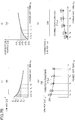
- FIG. 6A , FIG. 6B , and FIG. 6C each illustrate output energy correction method of a laser emitting element 41, which is performed by the controller 46.
- FIG. 6A illustrates an example of an electric current waveform (current waveform 500) of an electric current flowing through a laser emitting element 41, and (b) illustrates an output power waveform (output power waveform 510) illustrating output power of the laser emitting element 41 according to the current waveform 500.
- a target output is indicated by a broken line and an actual output is indicated by a solid line.
- (c) illustrates a current waveform 520 having a relatively long power-off time compared to a power-off time of the current waveform 500
- (d) illustrates an output power waveform 530 of output power of the laser emitting element 41 according to the current waveform 520.
- a target output is indicated by a broken line and an actual output is indicated by a solid line.
- a time-dependent change in an electric current 41S flowing through the laser emitting element 41 appears to form the current waveform 500 in (a) of FIG. 6A .
- the current waveform 500 has a power-off time t 1 during which no electric current flows between the formed pulse waveforms with a time width t 0 .
- the time width t 0 indicates a power-on time t 0 during which electric current flows.
- a time-dependent change in an optical power output from a laser emitting element 41 forms ideally close to a rectangular waveform, such as an output power waveform 510 as illustrated in (b) of FIG. 6A .
- the output energy per one output power waveform 510 is indicated by E 1 .
- a time-dependent change in the output power of the laser emitting element 41 may be an output power waveform 530 illustrated in (d) of FIG. 6A , where the rising edge is rounded, and output energy is E 2 that is less than E 1 .
- FIG. 6B illustrates a characteristic 540 of an optical temperature with a power-off time t off
- (f) illustrates a characteristic 550 of coupling efficiency with the power-off time t off estimated from the characteristic 540.
- (g) illustrates a characteristic 560 of output energy with the power-off time t off estimated from the characteristic 550
- (h) illustrates a characteristic 570 of correction energy with the power-off time t off estimated from the characteristic 560.
- the power-off times t 1 and t 2 (t 1 ⁇ t 2 ) illustrated in FIG. 6A are applied.
- the output energy per pulse waveform with the power-on time t 0 may be affected by the coupling efficiency characteristic illustrated by a graph 550 in (f) of FIG. 6B .
- the output energy per pulse waveform with the power-on time t 0 thus monotonically decreases as illustrated by a graph 560 in (g) of FIG. 6B (t 1 ⁇ t 2 , E 2 ⁇ E 1 ).
- the energy per one output power waveform with respect to a certain power-on time may be corrected so as to remain constant without being affected by the length of the power-off time.
- a correction energy characteristic for the power-off time may be set to compensate for the characteristic of the graph 550.
- the output energy per one pulse waveform is represented by E 1 + ⁇ E 1 , as illustrated in (j) of FIG. 6C .
- the output energy per one pulse waveform is represented by E 2 + ⁇ E 2 , as illustrated in (1) of FIG. 6C .
- the current value is set to be a constant I 1 .
- ⁇ t 1 satisfying the following equation (3) may be obtained by setting a constant value V 1 as a voltage between terminals of the laser emitting element 41, and setting t 0 as a pulse width correction start time. The same applies to ⁇ E 2 .
- ⁇ E 1 V 1 ⁇ ⁇ t 0 t 0 + ⁇ t 1 I t d t
- the method illustrated above is applied to one light source; however, a plurality of light sources is used as a fiber array in the actual device.
- PWM pulse width modulation
- an optical system temperature (graph 540 in (e) of FIG. 6B ) and a coupling efficiency characteristic (graph 550 in (f) of FIG. 6B ) are not necessarily the same for all the light sources, and are likely to differ between the light sources.
- the density of a recorded image typically becomes uneven because the energy per one output power waveform varies despite the fact that a current waveform with the same pulse width is input into the different light sources.
- a correction energy characteristic (graph 570 of (h) of FIG. 6B ), which is based on the optical system temperature (graph 540 of (e) of FIG. 6B ) and the coupling efficiency characteristic (graph 550 of (f) of FIG. 6B ), is required for each of the different light sources.
- a method of acquiring such a correction energy characteristic for the different light sources will be described with reference to FIGS. 7A and 7B .
- FIGS. 7A and 7B illustrate a method of acquiring the correction energy characteristic 570 for the different light sources.
- FIG. 7A illustrate respective waveforms 600, 620, 640, 660, and 680, which are current waveforms flowing into different laser emitting elements 41.
- time-dependent changes in the optical power output from the respective laser emitting elements 41 are represented by the output power waveforms 610, 630, 650, 670, and 690 illustrated in (b), (d), (f), (h), and (j) of FIG. 7A .
- FIG. 7B (k) illustrates a characteristic 700 between the output energies E 1 to E 5 and the power-off time t off , where the output energies E 1 to E 5 are based on the five types of inputs and outputs of FIG. 7A .
- the output energies E 1 to E 5 are based on the five types of inputs and outputs of FIG. 7A .
- the rise of the output power waveform decreases and the peak decreases.
- the energy per one output power waveform decreases with an increase in the power-off time, as illustrated in the graph 700.
- the correction energies may be added to E 1 to E 5 to make the output energies uniform.
- FIG. 7B (1) illustrates a characteristic 710 between the correction energies and the power-off time t off based on the graph 700.
- the characteristic 710 illustrates the correction energies ⁇ E 1 to ⁇ E 5 corresponding to E 1 to E 5 .
- the intercept of the characteristic of the graph 710 need not be zero because any value may be set as a value of Ec.
- a polynomial approximation of (t 1 ,E 1 ) to (t 5 ,E 5 ) on the graph 720 yields a variation function ⁇ (t off ) with the power-off time t off as a variable.
- a variation function ⁇ (t off ) is a polynomial, such as a linear function, a quadratic function, and a cubic function.
- the variation function ⁇ (t off ) may be represented by the following equation (4) (unit is ⁇ J).
- ⁇ t off a ⁇ t off 3 + b ⁇ t off 2 + c ⁇ t off + 250
- the intercept is determined to be 250 ⁇ J; however, the target energy and the intercept are not limited to these values.
- a correction function ⁇ (t off ) for setting the correction energy can also be calculated in order to reduce an energy variation.
- the correction function ⁇ (t off ) may, for example, be calculated by subtracting the variation function ⁇ (t off ) from the target energy Ec as indicated by the following equation (5).
- ⁇ t off Ec ⁇ ⁇ t off
- the correction function ⁇ can also be derived by other methods.
- a simple method readily prepared is to symmetrically move the variation function ⁇ (t off ) with respect to a horizontal axis (power-off time axis), and set the intercept to 0. That is, the correction function when the variation function is the equation (4) is represented by the following equation (6).
- ⁇ t off ⁇ a ⁇ t off 3 + b ⁇ t off 2 + c ⁇ t off
- the equations (5) and (6) are used to calculate the correction energies ⁇ E 1 to ⁇ E 5 with respect to respective waveforms 600, 620, 640, 660, and 680 illustrated in (a), (c), (e), (g), and (i) of FIG. 7A .
- the intercept is not necessarily zero.
- a correction function ⁇ (t off ) obtained is a graph 730 illustrated in (n) of FIG. 7B .
- the energy per one output power waveform is required for a plurality of power-off times with respect to a certain power-on time to.
- the maximum value of the power-off time for acquiring the function should preferably exceed a pixel period used in the actual device. For example, if a light source is driven at a pixel frequency of 40 kHz, a period of one pixel is 25 ⁇ s.
- the number of power-off times for acquiring the correction function is set to be five. However, if prioritizing accuracy, the number of power-off times may be increased, or if the correction function needs to be acquired in a shorter time, the number of power-off times may be decreased.
- an optical power meter or a thermal sensor having a large area of the photodetector it is possible to obtain optical energy output from a plurality of light sources without performing precise adjustment of the optical system. It is desirable that the optical system should be a system capable of inputting light from all the light sources to be used to the photodetector without adjusting the optical axis.
- the optical power meter and thermal sensor detect the time average (power) of the input optical energy. Thus, in order to measure the energy per one output power waveform, the detected power may be divided by the duty ratio. In this manner, an energy per one output power waveform may be obtained per unit time, and a comparison according to the power-off time may be possible as illustrated in the graph 720.
- correction functions ⁇ (t off ) may be obtained corresponding to a number of light sources less than the total number of light sources.
- FIG. 8 is a diagram illustrating examples of the characteristics of the correction function when the current value is variable. The vertical and horizontal axes of FIG. 8 are similar to those of (n) in FIG. 7B .
- the output device used in the present embodiment is basically assumed to perform pulse width modulation (PWM) with a fixed current value. If the current value is also modulated, it is necessary to acquire a plurality of correction functions ⁇ (t off ) corresponding to respective current values, as illustrated in a graph 740 of FIG. 8 .
- PWM pulse width modulation
- equation (6) may be multiplied by the polynomial ⁇ (I) with a current value as a variable, which is represented by the following equation (7) to be used as a correction function.
- ⁇ t off ⁇ a ⁇ t off 3 + b ⁇ t off 2 + c ⁇ t off ⁇ ⁇ I
- equation (7) may be multiplied by the polynomial A(t 0 ) with a power-on time t 0 as a variable, which is represented by the following equation (8) to be used as a correction function.
- ⁇ t off ⁇ a ⁇ t off 3 + b ⁇ t off 2 + c ⁇ t off ⁇ ⁇ I ⁇ A t 0
- FIG. 9 is a flowchart illustrating a process of calculating a correction function ⁇ (t off ). Each step in the process of the flowchart of FIG. 9 is performed in advance, for example, at every predetermined number of times, prior to performing a laser output operation by the controller 46.
- the process of the flowchart is executed on the assumption that, at a phase prior to the image recording device of FIG. 1 recording an image onto a recording target, a system for receiving laser light emitted from the laser emitting elements 41 of FIG. 4 is already disposed, and a correction function ⁇ (t off ) is calculated as correction information of the correction information database 470 stored in the controller 46 of FIG. 5 .
- the controller 46 selects a desired one of light sources from the laser emitting elements 41 (Step S1), sets a current value I (Step S2), a power-on time t 0 (Step S3), and a power-off time (Step S4), of an electric current flowing into the selected light source, and then outputs light from the selected light source of the laser emitting element 41 (Step S5).
- the method of detecting light differs according to whether the actual optical waveform is output (YES in Step S6) or the average power is detected (NO in Step S6).
- Step S6 When the actual optical waveform is output for detecting light (YES in Step S6), light is incident on a photodetector of a photodiode (PD) (Step S7), a current flowing through the PD is then converted into a voltage (Step S8), and an energy of one output power waveform is calculated based on a time-dependent change in the output power waveform displayed on a display by an oscilloscope and the like (Step S9).
- PD photodiode
- Step S6 When the average power is detected for detecting light (NO in Step S6), that is, light is incident on a photodetector of an optical power meter or of a thermal sensor (Step S10), an energy of one output power waveform per unit time is calculated by dividing the detected power by the duty ratio (Step S11).
- step S12 the process returns to step S4 to repeat the energy acquisition process.
- Step S12 a target energy Ec per one output power waveform is calculated (Step S13), and an energy variation function ⁇ (t off ) is calculated by polynomial approximation (Step S14).
- Step S15 an energy correction function ⁇ (t off ) is calculated based on the energy variation function ⁇ (t off ).
- the equation (5) can be used to calculate the energy correction function ⁇ (t off ) by subtracting the energy variation function ⁇ (t off ) from the target energy Ec.
- Step S16 When the number of the calculated correction functions ⁇ (t off ) is insufficient (NO in step S16), the process returns to Step 1 to select another one of light sources from the laser emitting elements 41. Meanwhile, when the number of the calculated correction functions ⁇ (t off ) is sufficient (YES in Step S16), this indicates that the number of the correction functions ⁇ required for being stored in the correction information database 470 of the controller 46 is obtained. The process of the control flowchart thus ends.
- FIG. 10 is a flowchart illustrating an operation of the driver 45 of the electric circuit illustrated in FIG. 5 . Each step of a process in the flowchart of FIG. 10 is performed by the controller 46.
- the process of the flowchart is executed on the assumption that the required number of correction functions ⁇ (t off ) is already obtained by the flowchart illustrated in FIG. 9 , at a phase before the image recording device of FIG. 1 records an image onto a recording target.
- the controller 46 transmits to the light emitting controller 455 a PWM control signal 455S as a switching signal (light emitting information) for switching the light emitting controller 455 on and off.
- the controller 46 corrects the control signal according to the flowchart illustrated in FIG. 10 , using the correction function ⁇ before transmitting the PWM control signal 455S.
- a correction energy ⁇ E is calculated by using the correction function ⁇ (t off ) (Step S102).
- an additional power-on time ⁇ t is calculated based on the calculated correction energy ⁇ E, the voltage V at two ends of the output units 454, and the current value I (Step S103).
- the controller 46 transmits the PWM control signal 455S, which has been corrected based on the corrected power-on time and power-off time, to the light emitting controller 455.
- the process of step S104 ends.
- FIG. 11 is a hardware configuration diagram illustrating a controller 46.
- the controller 46 may be configured as a computer system physically including a CPU (CPU) 101, a RAM (Random Access Memory) 102 as a main storage device, a ROM (Read Only Memory) 103, an input device 104 such as a keyboard and a mouse, an output device 105 such as a display and a touch panel, a communication module 106 as a data transmitting-receiving device such as a network card, and an auxiliary storage device 107 such as a hard disk.
- CPU CPU
- RAM Random Access Memory
- ROM Read Only Memory
- an input device 104 such as a keyboard and a mouse
- an output device 105 such as a display and a touch panel
- a communication module 106 as a data transmitting-receiving device such as a network card
- an auxiliary storage device 107 such as a hard disk.
- controller 46 The above-described functions of the controller 46 are implemented by reading predetermined computer software (output control program) on hardware such as the CPU 101 and the RAM 102, and operating the communication module 106, the input device 104, and the output device 105 under the control of the CPU 101, while reading and writing data in the RAM 102 and the auxiliary storage device 107.
- predetermined computer software output control program
- the output control program according to the present embodiment is stored, for example, in a storage device provided in a computer.
- the output control program may be configured such that a part or all of the output control program is transmitted through a transmission medium such as a communication line, and is received and recorded (including installation) by a communication module or the like provided in a computer.
- the manufacturing execution program may be configured to be recorded (including installation) in a computer from a state where a part or all of the manufacturing execution program is stored in a portable storage medium such as a CD-ROM, a DVD-ROM, or a flash memory.
- the controller 46 calculates a power-on time correction value ⁇ t using a correction function ⁇ (t off ) individually set for the laser emitting elements 41 on a per laser emitting element basis, and corrects a power-on time and a power-off time based on the calculated power-on time correction value ⁇ t.
- the output control device 140 when the output control device 140 records an image on a recording target by applying light emitted from a plurality of laser emitting elements 41 disposed in an array, and there are individual differences in modulation characteristics according to the laser emitting elements 41, the output control device 140 enables controlling output variations between the laser emitting elements 41 by correcting a length of the power-on time t 0 based on a length of the power-off time of a power supply to each of the laser emitting elements 41.
- a main scanning direction an arrangement direction of the laser emitting elements 41
- a movement direction of the recording target e.g., thermosensitive recording label RL illustrated in FIG. 1
- the correction function ⁇ (t off ) can be formulated as, for example, the equations (5) to (8) described above.
- the correction function ⁇ (t off ) is a function of the power-off time t off in each of the plurality of laser emitting elements 41. More specifically, the correction function ⁇ (t off ) may be expressed as a function configured to compensate for energy varying with the power-off time t off where the energy is output from the laser emitting element 41 at a given power-on time t 0 .
- the correction function ⁇ (t off ) may be expressed as a function that includes a polynomial function or an exponential function of the power-off time t off in each of the plurality of laser emitting elements 41. Furthermore, the correction function ⁇ (t off ) may be expressed as a monotonically increasing function having the power-off time t off as a variable. In addition, the correction function ⁇ (t off ) may be expressed as a function configured to compensate for an optical system temperature change or a coupling efficiency change of a light source of each of the plurality of laser emitting elements 41 with respect to the power-off time t off .
- the individual modulation characteristics of the plurality of laser emitting elements 41 can be expressed in a highly accurate manner according to the respective modulation characteristics. This can sufficiently reduce the differences in the modulation characteristics between the respective elements to make the outputs of the respective elements more uniform.
Landscapes
- Engineering & Computer Science (AREA)
- Multimedia (AREA)
- Signal Processing (AREA)
- Semiconductor Lasers (AREA)
Applications Claiming Priority (2)
| Application Number | Priority Date | Filing Date | Title |
|---|---|---|---|
| JP2019140259 | 2019-07-30 | ||
| JP2020121547A JP2021027340A (ja) | 2019-07-30 | 2020-07-15 | 出力制御装置、レーザー出力装置、画像記録装置、出力制御方法、及び、出力制御プログラム |
Publications (2)
| Publication Number | Publication Date |
|---|---|
| EP3772216A1 true EP3772216A1 (fr) | 2021-02-03 |
| EP3772216B1 EP3772216B1 (fr) | 2023-01-18 |
Family
ID=71846259
Family Applications (1)
| Application Number | Title | Priority Date | Filing Date |
|---|---|---|---|
| EP20188336.0A Active EP3772216B1 (fr) | 2019-07-30 | 2020-07-29 | Dispositif de commande de sortie, dispositif de sortie laser, dispositif d'enregistrement d'images, procédé de commande de sortie et programme de commande de sortie |
Country Status (1)
| Country | Link |
|---|---|
| EP (1) | EP3772216B1 (fr) |
Citations (4)
| Publication number | Priority date | Publication date | Assignee | Title |
|---|---|---|---|---|
| WO2003084013A1 (fr) * | 2002-03-29 | 2003-10-09 | Kataoka Corporation | Appareil laser solide |
| US20100260216A1 (en) * | 2009-04-09 | 2010-10-14 | Sumitomo Electric Industries, Ltd. | Pulse generation method and laser light source apparatus |
| US20150229095A1 (en) * | 2012-10-16 | 2015-08-13 | Furukawa Electric Co., Ltd. | Laser device |
| EP3210791A1 (fr) * | 2016-02-05 | 2017-08-30 | Ricoh Company, Ltd. | Procédé d'enregistrement et dispositif d'enregistrement |
-
2020
- 2020-07-29 EP EP20188336.0A patent/EP3772216B1/fr active Active
Patent Citations (5)
| Publication number | Priority date | Publication date | Assignee | Title |
|---|---|---|---|---|
| WO2003084013A1 (fr) * | 2002-03-29 | 2003-10-09 | Kataoka Corporation | Appareil laser solide |
| US20100260216A1 (en) * | 2009-04-09 | 2010-10-14 | Sumitomo Electric Industries, Ltd. | Pulse generation method and laser light source apparatus |
| US20150229095A1 (en) * | 2012-10-16 | 2015-08-13 | Furukawa Electric Co., Ltd. | Laser device |
| JP6077263B2 (ja) | 2012-10-16 | 2017-02-08 | 古河電気工業株式会社 | レーザ装置 |
| EP3210791A1 (fr) * | 2016-02-05 | 2017-08-30 | Ricoh Company, Ltd. | Procédé d'enregistrement et dispositif d'enregistrement |
Also Published As
| Publication number | Publication date |
|---|---|
| EP3772216B1 (fr) | 2023-01-18 |
Similar Documents
| Publication | Publication Date | Title |
|---|---|---|
| US9079422B2 (en) | Method and apparatus for printhead control based on neighbor printhead dot analysis | |
| EP3827995B1 (fr) | Appareil d'enregistrement d'images, procédé de commande de sortie, et programme de commande de sortie | |
| US10071586B2 (en) | Light irradiation apparatus and information rewritable system | |
| BR112013013531B1 (pt) | leitor operável para ler uma marca em um substrato e método de operação do mesmo | |
| JP2017013121A (ja) | レーザ光照射装置及びリライタブルレーザシステム | |
| JP6589999B2 (ja) | 画像記録装置および画像記録方法 | |
| EP3772216A1 (fr) | Dispositif de commande de sortie, dispositif de sortie laser, dispositif d'enregistrement d'images, procédé de commande de sortie et programme de commande de sortie | |
| JPH07137327A (ja) | サーマルヘッドの発熱体の駆動装置 | |
| JP7135564B2 (ja) | 出力制御装置、出力制御方法、出力制御を用いたレーザー出力装置、及びレーザー出力装置を用いた画像記録装置 | |
| EP3412469B1 (fr) | Appareil d'enregistrement d'image et procédé d'enregistrement d'image | |
| JP2021027340A (ja) | 出力制御装置、レーザー出力装置、画像記録装置、出力制御方法、及び、出力制御プログラム | |
| EP3820710B1 (fr) | Procédé d'impression laser et dispositif d'impression laser | |
| US9370939B2 (en) | Method and apparatus for printer control | |
| RU2571255C1 (ru) | Устройство обработки информации, способ обработки информации, система обработки информации, компьютерная программа и компьютерно-читаемый носитель | |
| EP3412468B1 (fr) | Appareil d'enregistrement d'image et procédé d'enregistrement d'image | |
| JP2008137244A (ja) | 非接触光書き込み装置 | |
| JP2020157765A (ja) | レーザ記録装置、レーザ記録方法、及びレーザ記録用レーザ照射プログラム |
Legal Events
| Date | Code | Title | Description |
|---|---|---|---|
| PUAI | Public reference made under article 153(3) epc to a published international application that has entered the european phase |
Free format text: ORIGINAL CODE: 0009012 |
|
| STAA | Information on the status of an ep patent application or granted ep patent |
Free format text: STATUS: REQUEST FOR EXAMINATION WAS MADE |
|
| 17P | Request for examination filed |
Effective date: 20200729 |
|
| AK | Designated contracting states |
Kind code of ref document: A1 Designated state(s): AL AT BE BG CH CY CZ DE DK EE ES FI FR GB GR HR HU IE IS IT LI LT LU LV MC MK MT NL NO PL PT RO RS SE SI SK SM TR |
|
| AX | Request for extension of the european patent |
Extension state: BA ME |
|
| GRAP | Despatch of communication of intention to grant a patent |
Free format text: ORIGINAL CODE: EPIDOSNIGR1 |
|
| STAA | Information on the status of an ep patent application or granted ep patent |
Free format text: STATUS: GRANT OF PATENT IS INTENDED |
|
| INTG | Intention to grant announced |
Effective date: 20220916 |
|
| GRAS | Grant fee paid |
Free format text: ORIGINAL CODE: EPIDOSNIGR3 |
|
| GRAA | (expected) grant |
Free format text: ORIGINAL CODE: 0009210 |
|
| STAA | Information on the status of an ep patent application or granted ep patent |
Free format text: STATUS: THE PATENT HAS BEEN GRANTED |
|
| AK | Designated contracting states |
Kind code of ref document: B1 Designated state(s): AL AT BE BG CH CY CZ DE DK EE ES FI FR GB GR HR HU IE IS IT LI LT LU LV MC MK MT NL NO PL PT RO RS SE SI SK SM TR |
|
| REG | Reference to a national code |
Ref country code: GB Ref legal event code: FG4D |
|
| REG | Reference to a national code |
Ref country code: DE Ref legal event code: R096 Ref document number: 602020007639 Country of ref document: DE |
|
| REG | Reference to a national code |
Ref country code: CH Ref legal event code: EP |
|
| REG | Reference to a national code |
Ref country code: AT Ref legal event code: REF Ref document number: 1545283 Country of ref document: AT Kind code of ref document: T Effective date: 20230215 Ref country code: IE Ref legal event code: FG4D |
|
| REG | Reference to a national code |
Ref country code: LT Ref legal event code: MG9D |
|
| REG | Reference to a national code |
Ref country code: NL Ref legal event code: MP Effective date: 20230118 |
|
| REG | Reference to a national code |
Ref country code: AT Ref legal event code: MK05 Ref document number: 1545283 Country of ref document: AT Kind code of ref document: T Effective date: 20230118 |
|
| PG25 | Lapsed in a contracting state [announced via postgrant information from national office to epo] |
Ref country code: NL Free format text: LAPSE BECAUSE OF FAILURE TO SUBMIT A TRANSLATION OF THE DESCRIPTION OR TO PAY THE FEE WITHIN THE PRESCRIBED TIME-LIMIT Effective date: 20230118 |
|
| PG25 | Lapsed in a contracting state [announced via postgrant information from national office to epo] |
Ref country code: RS Free format text: LAPSE BECAUSE OF FAILURE TO SUBMIT A TRANSLATION OF THE DESCRIPTION OR TO PAY THE FEE WITHIN THE PRESCRIBED TIME-LIMIT Effective date: 20230118 Ref country code: PT Free format text: LAPSE BECAUSE OF FAILURE TO SUBMIT A TRANSLATION OF THE DESCRIPTION OR TO PAY THE FEE WITHIN THE PRESCRIBED TIME-LIMIT Effective date: 20230518 Ref country code: NO Free format text: LAPSE BECAUSE OF FAILURE TO SUBMIT A TRANSLATION OF THE DESCRIPTION OR TO PAY THE FEE WITHIN THE PRESCRIBED TIME-LIMIT Effective date: 20230418 Ref country code: LV Free format text: LAPSE BECAUSE OF FAILURE TO SUBMIT A TRANSLATION OF THE DESCRIPTION OR TO PAY THE FEE WITHIN THE PRESCRIBED TIME-LIMIT Effective date: 20230118 Ref country code: LT Free format text: LAPSE BECAUSE OF FAILURE TO SUBMIT A TRANSLATION OF THE DESCRIPTION OR TO PAY THE FEE WITHIN THE PRESCRIBED TIME-LIMIT Effective date: 20230118 Ref country code: HR Free format text: LAPSE BECAUSE OF FAILURE TO SUBMIT A TRANSLATION OF THE DESCRIPTION OR TO PAY THE FEE WITHIN THE PRESCRIBED TIME-LIMIT Effective date: 20230118 Ref country code: ES Free format text: LAPSE BECAUSE OF FAILURE TO SUBMIT A TRANSLATION OF THE DESCRIPTION OR TO PAY THE FEE WITHIN THE PRESCRIBED TIME-LIMIT Effective date: 20230118 Ref country code: AT Free format text: LAPSE BECAUSE OF FAILURE TO SUBMIT A TRANSLATION OF THE DESCRIPTION OR TO PAY THE FEE WITHIN THE PRESCRIBED TIME-LIMIT Effective date: 20230118 |
|
| P01 | Opt-out of the competence of the unified patent court (upc) registered |
Effective date: 20230714 |
|
| PG25 | Lapsed in a contracting state [announced via postgrant information from national office to epo] |
Ref country code: SE Free format text: LAPSE BECAUSE OF FAILURE TO SUBMIT A TRANSLATION OF THE DESCRIPTION OR TO PAY THE FEE WITHIN THE PRESCRIBED TIME-LIMIT Effective date: 20230118 Ref country code: PL Free format text: LAPSE BECAUSE OF FAILURE TO SUBMIT A TRANSLATION OF THE DESCRIPTION OR TO PAY THE FEE WITHIN THE PRESCRIBED TIME-LIMIT Effective date: 20230118 Ref country code: IS Free format text: LAPSE BECAUSE OF FAILURE TO SUBMIT A TRANSLATION OF THE DESCRIPTION OR TO PAY THE FEE WITHIN THE PRESCRIBED TIME-LIMIT Effective date: 20230518 Ref country code: GR Free format text: LAPSE BECAUSE OF FAILURE TO SUBMIT A TRANSLATION OF THE DESCRIPTION OR TO PAY THE FEE WITHIN THE PRESCRIBED TIME-LIMIT Effective date: 20230419 Ref country code: FI Free format text: LAPSE BECAUSE OF FAILURE TO SUBMIT A TRANSLATION OF THE DESCRIPTION OR TO PAY THE FEE WITHIN THE PRESCRIBED TIME-LIMIT Effective date: 20230118 |
|
| REG | Reference to a national code |
Ref country code: DE Ref legal event code: R097 Ref document number: 602020007639 Country of ref document: DE |
|
| PG25 | Lapsed in a contracting state [announced via postgrant information from national office to epo] |
Ref country code: SM Free format text: LAPSE BECAUSE OF FAILURE TO SUBMIT A TRANSLATION OF THE DESCRIPTION OR TO PAY THE FEE WITHIN THE PRESCRIBED TIME-LIMIT Effective date: 20230118 Ref country code: RO Free format text: LAPSE BECAUSE OF FAILURE TO SUBMIT A TRANSLATION OF THE DESCRIPTION OR TO PAY THE FEE WITHIN THE PRESCRIBED TIME-LIMIT Effective date: 20230118 Ref country code: EE Free format text: LAPSE BECAUSE OF FAILURE TO SUBMIT A TRANSLATION OF THE DESCRIPTION OR TO PAY THE FEE WITHIN THE PRESCRIBED TIME-LIMIT Effective date: 20230118 Ref country code: DK Free format text: LAPSE BECAUSE OF FAILURE TO SUBMIT A TRANSLATION OF THE DESCRIPTION OR TO PAY THE FEE WITHIN THE PRESCRIBED TIME-LIMIT Effective date: 20230118 Ref country code: CZ Free format text: LAPSE BECAUSE OF FAILURE TO SUBMIT A TRANSLATION OF THE DESCRIPTION OR TO PAY THE FEE WITHIN THE PRESCRIBED TIME-LIMIT Effective date: 20230118 |
|
| PGFP | Annual fee paid to national office [announced via postgrant information from national office to epo] |
Ref country code: IT Payment date: 20230731 Year of fee payment: 4 Ref country code: CH Payment date: 20230801 Year of fee payment: 4 |
|
| PLBE | No opposition filed within time limit |
Free format text: ORIGINAL CODE: 0009261 |
|
| STAA | Information on the status of an ep patent application or granted ep patent |
Free format text: STATUS: NO OPPOSITION FILED WITHIN TIME LIMIT |
|
| PG25 | Lapsed in a contracting state [announced via postgrant information from national office to epo] |
Ref country code: SK Free format text: LAPSE BECAUSE OF FAILURE TO SUBMIT A TRANSLATION OF THE DESCRIPTION OR TO PAY THE FEE WITHIN THE PRESCRIBED TIME-LIMIT Effective date: 20230118 |
|
| PGFP | Annual fee paid to national office [announced via postgrant information from national office to epo] |
Ref country code: FR Payment date: 20230726 Year of fee payment: 4 Ref country code: DE Payment date: 20230719 Year of fee payment: 4 |
|
| 26N | No opposition filed |
Effective date: 20231019 |
|
| PG25 | Lapsed in a contracting state [announced via postgrant information from national office to epo] |
Ref country code: SI Free format text: LAPSE BECAUSE OF FAILURE TO SUBMIT A TRANSLATION OF THE DESCRIPTION OR TO PAY THE FEE WITHIN THE PRESCRIBED TIME-LIMIT Effective date: 20230118 |
|
| PG25 | Lapsed in a contracting state [announced via postgrant information from national office to epo] |
Ref country code: MC Free format text: LAPSE BECAUSE OF FAILURE TO SUBMIT A TRANSLATION OF THE DESCRIPTION OR TO PAY THE FEE WITHIN THE PRESCRIBED TIME-LIMIT Effective date: 20230118 |
|
| PG25 | Lapsed in a contracting state [announced via postgrant information from national office to epo] |
Ref country code: MC Free format text: LAPSE BECAUSE OF FAILURE TO SUBMIT A TRANSLATION OF THE DESCRIPTION OR TO PAY THE FEE WITHIN THE PRESCRIBED TIME-LIMIT Effective date: 20230118 |
|
| REG | Reference to a national code |
Ref country code: BE Ref legal event code: MM Effective date: 20230731 |
|
| PG25 | Lapsed in a contracting state [announced via postgrant information from national office to epo] |
Ref country code: LU Free format text: LAPSE BECAUSE OF NON-PAYMENT OF DUE FEES Effective date: 20230729 |
|
| PG25 | Lapsed in a contracting state [announced via postgrant information from national office to epo] |
Ref country code: LU Free format text: LAPSE BECAUSE OF NON-PAYMENT OF DUE FEES Effective date: 20230729 |
|
| REG | Reference to a national code |
Ref country code: IE Ref legal event code: MM4A |