EP3772097A1 - Lead frame for a package for a semiconductor device, semiconductor device and process for manufacturing a semiconductor device - Google Patents
Lead frame for a package for a semiconductor device, semiconductor device and process for manufacturing a semiconductor device Download PDFInfo
- Publication number
- EP3772097A1 EP3772097A1 EP20189128.0A EP20189128A EP3772097A1 EP 3772097 A1 EP3772097 A1 EP 3772097A1 EP 20189128 A EP20189128 A EP 20189128A EP 3772097 A1 EP3772097 A1 EP 3772097A1
- Authority
- EP
- European Patent Office
- Prior art keywords
- die pad
- lead frame
- top coating
- region
- die
- Prior art date
- Legal status (The legal status is an assumption and is not a legal conclusion. Google has not performed a legal analysis and makes no representation as to the accuracy of the status listed.)
- Granted
Links
Images





Classifications
-
- H—ELECTRICITY
- H10—SEMICONDUCTOR DEVICES; ELECTRIC SOLID-STATE DEVICES NOT OTHERWISE PROVIDED FOR
- H10W—GENERIC PACKAGES, INTERCONNECTIONS, CONNECTORS OR OTHER CONSTRUCTIONAL DETAILS OF DEVICES COVERED BY CLASS H10
- H10W70/00—Package substrates; Interposers; Redistribution layers [RDL]
- H10W70/01—Manufacture or treatment
- H10W70/04—Manufacture or treatment of leadframes
- H10W70/042—Etching
-
- H—ELECTRICITY
- H10—SEMICONDUCTOR DEVICES; ELECTRIC SOLID-STATE DEVICES NOT OTHERWISE PROVIDED FOR
- H10W—GENERIC PACKAGES, INTERCONNECTIONS, CONNECTORS OR OTHER CONSTRUCTIONAL DETAILS OF DEVICES COVERED BY CLASS H10
- H10W70/00—Package substrates; Interposers; Redistribution layers [RDL]
- H10W70/40—Leadframes
- H10W70/411—Chip-supporting parts, e.g. die pads
-
- H—ELECTRICITY
- H10—SEMICONDUCTOR DEVICES; ELECTRIC SOLID-STATE DEVICES NOT OTHERWISE PROVIDED FOR
- H10W—GENERIC PACKAGES, INTERCONNECTIONS, CONNECTORS OR OTHER CONSTRUCTIONAL DETAILS OF DEVICES COVERED BY CLASS H10
- H10W70/00—Package substrates; Interposers; Redistribution layers [RDL]
- H10W70/40—Leadframes
- H10W70/421—Shapes or dispositions
-
- H—ELECTRICITY
- H10—SEMICONDUCTOR DEVICES; ELECTRIC SOLID-STATE DEVICES NOT OTHERWISE PROVIDED FOR
- H10W—GENERIC PACKAGES, INTERCONNECTIONS, CONNECTORS OR OTHER CONSTRUCTIONAL DETAILS OF DEVICES COVERED BY CLASS H10
- H10W70/00—Package substrates; Interposers; Redistribution layers [RDL]
- H10W70/40—Leadframes
- H10W70/456—Materials
- H10W70/458—Materials of insulating layers on leadframes
-
- H—ELECTRICITY
- H10—SEMICONDUCTOR DEVICES; ELECTRIC SOLID-STATE DEVICES NOT OTHERWISE PROVIDED FOR
- H10W—GENERIC PACKAGES, INTERCONNECTIONS, CONNECTORS OR OTHER CONSTRUCTIONAL DETAILS OF DEVICES COVERED BY CLASS H10
- H10W70/00—Package substrates; Interposers; Redistribution layers [RDL]
- H10W70/40—Leadframes
- H10W70/464—Additional interconnections in combination with leadframes
- H10W70/465—Bumps or wires
-
- H—ELECTRICITY
- H10—SEMICONDUCTOR DEVICES; ELECTRIC SOLID-STATE DEVICES NOT OTHERWISE PROVIDED FOR
- H10W—GENERIC PACKAGES, INTERCONNECTIONS, CONNECTORS OR OTHER CONSTRUCTIONAL DETAILS OF DEVICES COVERED BY CLASS H10
- H10W72/00—Interconnections or connectors in packages
- H10W72/071—Connecting or disconnecting
- H10W72/075—Connecting or disconnecting of bond wires
-
- H—ELECTRICITY
- H10—SEMICONDUCTOR DEVICES; ELECTRIC SOLID-STATE DEVICES NOT OTHERWISE PROVIDED FOR
- H10W—GENERIC PACKAGES, INTERCONNECTIONS, CONNECTORS OR OTHER CONSTRUCTIONAL DETAILS OF DEVICES COVERED BY CLASS H10
- H10W74/00—Encapsulations, e.g. protective coatings
- H10W74/10—Encapsulations, e.g. protective coatings characterised by their shape or disposition
- H10W74/111—Encapsulations, e.g. protective coatings characterised by their shape or disposition the semiconductor body being completely enclosed
- H10W74/129—Encapsulations, e.g. protective coatings characterised by their shape or disposition the semiconductor body being completely enclosed forming a chip-scale package [CSP]
-
- H—ELECTRICITY
- H10—SEMICONDUCTOR DEVICES; ELECTRIC SOLID-STATE DEVICES NOT OTHERWISE PROVIDED FOR
- H10W—GENERIC PACKAGES, INTERCONNECTIONS, CONNECTORS OR OTHER CONSTRUCTIONAL DETAILS OF DEVICES COVERED BY CLASS H10
- H10W70/00—Package substrates; Interposers; Redistribution layers [RDL]
- H10W70/40—Leadframes
- H10W70/456—Materials
- H10W70/457—Materials of metallic layers on leadframes
-
- H—ELECTRICITY
- H10—SEMICONDUCTOR DEVICES; ELECTRIC SOLID-STATE DEVICES NOT OTHERWISE PROVIDED FOR
- H10W—GENERIC PACKAGES, INTERCONNECTIONS, CONNECTORS OR OTHER CONSTRUCTIONAL DETAILS OF DEVICES COVERED BY CLASS H10
- H10W74/00—Encapsulations, e.g. protective coatings
- H10W74/01—Manufacture or treatment
-
- H—ELECTRICITY
- H10—SEMICONDUCTOR DEVICES; ELECTRIC SOLID-STATE DEVICES NOT OTHERWISE PROVIDED FOR
- H10W—GENERIC PACKAGES, INTERCONNECTIONS, CONNECTORS OR OTHER CONSTRUCTIONAL DETAILS OF DEVICES COVERED BY CLASS H10
- H10W74/00—Encapsulations, e.g. protective coatings
- H10W74/10—Encapsulations, e.g. protective coatings characterised by their shape or disposition
- H10W74/111—Encapsulations, e.g. protective coatings characterised by their shape or disposition the semiconductor body being completely enclosed
Definitions
- the present invention relates to a lead frame for a package for a semiconductor device, as well as to a semiconductor device and to a process for manufacturing a semiconductor device.
- semiconductor devices such as for example integrated circuits and MEMS devices
- packages which perform functions of protection and interfacing with the outside world.
- packages are known that enable so-called "surface mounting" on a printed-circuit board.
- surface-mount packages include, for example, the so-called packages of a “quad-flat no-leads” (QFN) type, also known as “micro lead frame” (MLF) packages or “small-outline no-leads” (SON) packages.
- QFN quad-flat no-leads
- MLF micro lead frame
- SON small-outline no-leads
- a QFN package comprises a region of resin, englobed inside which is a metallic lead frame (typically, made up of copper), which in turn forms at least one array of terminals that give out onto a bottom surface of the package.
- a metallic lead frame typically, made up of copper
- a lead frame 1 includes a main body 2, which is planar and has, in top plan view, a polygonal shape (typically, a square or a rectangle); the main body 2 defines a top surface 6a and a bottom surface 6b.
- a plurality of pads 8 extend upwards from the main body 2, i.e. from the top surface 6a.
- the lead frame 1 comprises the so-called die pad 10, which extend upwards from the main body 2 and is surrounded, at distance, by the inner pads 8.
- the main body 2, the pads 8 and the die pad 10 form one single piece of metal.
- the die pad 10 is planar and has, in top plan view, a polygonal shape (typically, a square or a rectangle) .
- the die pad 10 has the shape of a parallelepiped and its lateral walls 16 define four edges 11 (only three visible in Figure 1 ).
- the lead frame 1 is plated, usually by means of silver or a metallic alloy (such as NiPdAu).
- the lead frame 1 undergoes a plating process (e.g., an electroplating) which allows to form a top coating region 12 on the die pad 10, and a plurality of secondary coating regions 14, each of which is arranged on a corresponding pad 8.
- the top coating region 12 and the secondary coating region 14 are formed by silver or a metallic alloy, i.e. by a material which is less prone to oxidation (in particular, oxidation in air) than the material forming the lead frame 1 (i.e., by a material having a lower oxidation rate than the lead frame).
- the top coating region 12 and the secondary coating region 14 may have a thickness comprised in the range 3-9 ⁇ m; the pads 8 and the die pad 10 may have a thickness comprised in the range 3-4 ⁇ m.
- lead frames are manufactured in strips, which are subsequently used in the manufacturing processes. Furthermore, the manufacturing processes typically comprise a step of back-etching to remove the main body 2 and separate the pads 8 from the die pad 10.
- the manufacturing processes typically include the steps of setting the die (not shown) on the die pad 10, and then electrically connecting the conductive pads of the die to corresponding pads 8 of the lead frame 1, by means of wire bondings 24, as shown in Figure 3 .
- a thermal treatment is carried out, usually at a temperature of about 200°C, in air, and with a duration of about ten minutes; such a thermal treatment causes a controlled oxidation of the exposed parts of the lead frame 1, i.e. of the parts of the lead frame 1 not coated by the top coating region 12, nor by the secondary coating regions 14. Therefore, after the thermal treatment, an oxidized layer 27 extends on parts of the lead frame 1, as well as under the lead frame 1.
- a packaging region 25 is then formed, typically by means of moulding, on top of the lead frame 1 and the die.
- the packaging region 25, also known as “moulding compound”, may be made of a thermosetting epoxy resin and extends in direct contact with part of the top coating region 12, as well as with the secondary coating regions 14 and with the oxidized layer 27.
- the lead frame 1 may include a die pad structure 28 including the die pad 10, a ground ring 29 which laterally surrounds the die pad 10, and a trench T0 extending between the die pad 10 and the ground ring 29, so as to expose a corresponding portion of the underlying main body 2.
- the ground ring 29 extends upwards from the main body 2, has the same thickness as the die pad 10 and has the shape of a squared frame; the ground ring 29 forms a single piece with the main body 2, the die pad 10 and the pads 8 The pads 8 surround the die pad structure 28.
- the ground ring 29 is coated, at top, by an additional coating region 12' , which is made of the same material as the top coating region 12 and has the same thickness as this latter.
- the difference between the coefficients of thermal expansion (CTE) of the packaging region 25 and the lead frame 1 may cause mechanical stresses, due to temperature changes which occur during the functioning of the electronic device implemented in the die.
- a first solution envisages the use of additional adhesion promoter materials to be applied on the lead frame surface.
- additional adhesion promoter materials to be applied on the lead frame surface.
- a second solution envisages the formation of holding structures (such as grooves or dimples) in the lead frame.
- holding structures such as grooves or dimples
- US 2016/0355655 discloses a packaged device comprising a lead frame and a plurality of capacitors, which are attached to surface portions of structures of the lead frame.
- JP H03 149865 discloses a method for enhancing the adhesion of the sealing resin of a package to a die pad, by forming a plating of the die pad as large as, or smaller than, the die, leaving exposed a peripheral portion.
- the aim of the present invention is thus to provide a lead frame for a semiconductor device that will solve at least in part the drawbacks of the known art.
- a lead frame for a semiconductor device a semiconductor device and a process for manufacturing a semiconductor device are provided, as defined in the appended claims.
- the present lead frame stems from the idea of leaving exposed the corners of the die pad structure, so as to create sacrificial oxidized regions which allow to limit the delamination, as described here below, with reference to a lead frame of the type shown in Figure 1 , without this implying any limitation. Therefore, the following description will limit to the differences over the lead frame 1 shown in Figure 1 ; in addition, the same reference signs will be used, unless stated otherwise.
- Figures 5 and 6 show a lead frame (here designated by 101), in which the die pad (here designated by 110) has the same shape as the die pad 10 of Figures 1 and 2 .
- the die pad 110 is delimited at top by a front surface 103.
- the top coating region (here designated by 112) extends on the front surface 103, in direct contact.
- the top coating region 112 leaves exposed four corner portions 117 of the die pad 110, which are delimited at top by corresponding portions of the top surface 103, hereinafter referred to as the top angular surface portions 117S.
- each corner portion 117 includes a corresponding edge (here designated by 111) of the die pad 110, perpendicular to the front surface 103 and in contact with this latter.
- the four corner portions 117 have one and the same shape; in particular, in top plan view, the corner portions 117 have the shape of a square.
- Each top angular surface portion 117S extends from a corresponding edge 111 and is separate from the other top angular surface portions 117S; in top view, each top angular surface portion 117S extends from a corresponding vertex of the polygonal shape defined by the top coating region 112.
- the top coating region 112 covers, in direct contact, the whole front surface 103 of the die pad 110, except the top angular surface portions 117S.
- the corresponding thermal treatment leads to the formation of a bottom oxidized layer 126, extending under the bottom surface 6b, and a top oxidized layer 127, as shown in Figure 7 .
- the bottom oxidized layer 126 and the top oxidized layer 127 may have a thickness comprised, as an example, in the range 100nm-200nm.
- the top oxidized region 127 includes a main portion 128, which extends on the top surface 6a of the main body 2, as well as on the side walls of the pads 8 and the die pad 110; therefore, the main portion 128 of the top oxidized region 127 coats the edges 111 of the die pad 110.
- the top oxidized region 127 comprises four additional portions 129 (only one visible in Figure 7 ), hereinafter referred to as the sacrificial portions 129.
- each sacrificial portion 129 extends on a corresponding corner portion 117 of the die pad 110, i.e. on a corresponding top angular surface portion 117S.
- each sacrificial portion 129 is laterally staggered with respect to the top coating region 112, with which it is in direct contact, thereby forming a corresponding interface IF.
- the packaging region 25 extends, among other things, also on the sacrificial portions 129.
- the abovementioned curing step causes mechanical stresses due to CTE (coefficient of thermal expansion) mismatch which are unlikely to cause a delamination between the sacrificial portions 129 and the packaging region 25, for the following reasons.
- the Applicant has noticed that the adhesion between the top oxidized region 127 and the packaging region 25 is greater than the adhesion between the top oxidized region 127 and the lead frame 101.
- the adhesion between the corresponding sacrificial portion 129 and the overlying portion of the packaging region 25 is greater than the adhesion between the sacrificial portion 129 and the underlying corner portion 117 of the die pad 110.
- delamination may occur, at most, between the sacrificial portions 129 and the die pad 110; furthermore, such a delamination does not propagate beyond the interface IF between each sacrificial portion 129 and the top coating region 112, therefore it does not affect the adhesion between the packaging region 25 and the top coating region 112. Therefore, the packaging region 25 and the top coating region 112 continue to encapsulate the die, without exposing this latter to the external atmosphere.
- the reduced size of the top angular surface portion 117S with respect to the top coating region 112 contributes to achieving this result.
- Figure 9 shows a further embodiment, which will be described hereinbelow with reference to the differences over the lead frame shown in Figure 4 .
- the additional coating region 12' leaves exposed four corner portions 217 of the ground ring 29, which are delimited at top by corresponding portions of the additional front surface 103', hereinafter referred to as the additional top angular surface portions 217S.
- the additional coating region 12' covers, in direct contact, the whole additional front surface 103', except the additional top angular surface portions 217S, which are separate from one another.
- each top angular surface portion 217S has the shape of an "L".
- each additional top angular surface portions 217S gets coated by a corresponding oxidized sacrificial region (not shown). Therefore, the embodiment shown in Figure 9 guarantees the same advantages as the one shown in Figures 6-8 .
- FIGS 10-12 show a further embodiment, in which the lead frame, here designated by 301, is suitable to form a package of the so-called thin quad flat pack (TQFP) type.
- TQFP thin quad flat pack
- the lead frame 301 includes a die pad 310 with a squared planar shape, delimited at top and at bottom, respectively, by the front surface, here designated by 303 (visible in Figure 11 ), and by a rear surface 405.
- the top coating region, here designated by 312 leaves exposed only the four top angular surface portions, here designated by 317S.
- the edges (here designated by 311) of the die pad 310 are bevelled. Each edge 311 is still formed by a corresponding pair of adjacent side walls (here designated by 316) of the die pad 310.
- the rear surface 405 is coated, in direct contact, by a bottom coating region 412, which is formed by the same material as the top coating region 312 (as an example, silver) and leaves exposed only four corner portions 417S of the rear surface 405, hereinafter referred to as the bottom angular surface portions 417S.
- a bottom coating region 412 which is formed by the same material as the top coating region 312 (as an example, silver) and leaves exposed only four corner portions 417S of the rear surface 405, hereinafter referred to as the bottom angular surface portions 417S.
- a pair of (optional) trenches with concentric squared annular shapes may be present.
- a first and a second trench T1, T2 may extend through the bottom coating region 412 and part of the die pad 310, with a rectangular cross-section.
- the second trench T2 surrounds, at distance, the first trench T1; furthermore, the first and second trenches T1, T2 do not completely cross the die pad 310 (i.e., they are blind) and extend in such a way that, as shown in Figure 12 , each bottom angular surface portion 417S is divided into a first, a second and a third exposed subportion 418A, 418B, 418C, the first trench T1 extending, in bottom view, between the first and the second exposed subportions 418A, 418B, the second trench T2 extending between the second and the third exposed subportions 418B, 418C.
- the first exposed subportion 418A is arranged inwardly, whereas the third exposed subportion 418C is arranged outwardly, towards the corresponding edge 311; the second exposed subportion 418B is interposed between the first and the third exposed subportions 418A, 418C.
- the lead frame 310 comprises an inner frame 450 which is squared and planar and surrounds, at distance, the die pad 310, to which it is connected by means of a plurality of bridges 451.
- the die pad 310, the bridges 451 and the inner frame 450 form one single piece of metal (i.e., they are made up of one and the same material); in addition, the inner frame 450 may be vertically staggered with respect to the die pad 310, i.e. it may be arranged at an height (measured in a direction perpendicular to the die pad 310) higher than the die pad 310.
- the inner frame 450 is delimited at top and at bottom by, respectively, a top frame surface 452 and a bottom frame surface 453.
- each top frame surface portions 457S has the shape of an "L", whose concavity houses part of the corresponding top angular surface portion 317S.
- each bottom frame surface portion 467S has the shape of an "L”, whose concavity houses the corresponding third exposed subportion 418C.
- Each bottom frame surface portion 467S and the corresponding top frame surface portion 457S delimit, respectively at top and at bottom, a corresponding corner portion 499 of the inner frame 450.
- the lead frame 301 further comprises an outer frame 470, which is planar and squared and surrounds, at distance, the inner frame 450, and a plurality of cantilever leads 472, each cantilever lead 472 being fixed to the outer frame 470 and extending towards the inner frame 450.
- the outer frame 470 may be vertically staggered with respect to the inner frame 450, and in particular it may be arranged at an height higher than the inner frame 450.
- the die pad 310, the inner frame 450 and the outer frame 470 lie in corresponding planes which, though arranged at different heights, are parallel.
- the lead frame 301 comprises four connecting elements 474, hereinafter referred to as tie bars 474.
- Each tie bar 474 has an elongated shape and two ends, a first end being fixed to the inner frame 450, the second end being fixed to the outer frame 470.
- the die pad 310, the inner frame 450, the outer frame 470, the cantilever leads 472 and the tie bars 474 form a single metallic piece.
- Each tie bar 474 is delimited at top and at bottom by, respectively, a respective top surface 493 and a respective bottom surface 495. Furthermore, each tie bar 474 comprises a slanted portion 475A and a planar portion 475B. The planar portion 475B connects to the outer frame 470. The slanted portion 475A is interposed between the inner frame 450 and the planar portion 475B; in particular, the slanted portion 475A connects to a corresponding corner portion 499 of the inner frame 450. In addition, either the top surface 493 and the bottom surface 495 have the shape of a pair of plane surfaces connected to one another (i.e, one slanted plane surface and an horizontal plane surface, connected to one another).
- the upper sides of the cantilever leads 472 and of the outer frame 470 are coated by an outer top coating region 512; the lower sides of the cantilever leads 472 and of the outer frame 470 are coated by an outer bottom coating region 613.
- the outer top coating region 512 and the outer bottom coating region 613 may be formed by the same metallic material as the top coating region 312 and the bottom coating region 412.
- the outer top coating region 512 leaves exposed a portion 517S of the top surface 493 of each tie bar 474, hereinafter referred to as the exposed top elongated surface 517S.
- Each exposed top elongated surface 517S connects to a corresponding top frame surface portion 457S.
- the outer bottom coating region 613 leaves exposed a portion 617S of the bottom surface 493 of each tie bar 474, hereinafter referred to as the exposed bottom elongated surface 617S.
- Each exposed bottom elongated surface 617S connects to a corresponding bottom frame surface portion 467S.
- the lead frame 301 may be used to manufacture an integrated electronic device 700, which includes a die 502, fixed on a portion of the top coating region 312 covering the die pad 310, by means of an interposed layer 503 of epoxy conductive glue, silver filled.
- the packaging region 25 englobes the lead frame 301, which has previously undergone a cutting process which, in a per se know manner, led to the removal of the outer frame 470, as well as of parts of the cantilever leads 472 and of the tie bars 474 connected thereto.
- the packaging region 25 leaves exposed the bottom coating region 412 and part of each tie bar 474.
- outer parts of the exposed top elongated surface 517S and of the exposed bottom elongated surface 617S extend outside the packaging region 25; inner parts of the exposed top elongated surface 517S and of the exposed bottom elongated surface 617S extend inside the packaging region 25.
- parts of the tie bar 474 covered, on opposite sides, by the outer top coating region 512 and the outer bottom coating region 613 extend outside the packaging region 25.
- each exposed top elongated surface 517S and the corresponding top frame surface portion 457S are coated by a corresponding top oxidized region 800; each exposed bottom elongated surface 617S and the corresponding bottom frame surface portion 467S are coated by a bottom oxidized region 802, forming one single oxidized region with the top oxidized region 800.
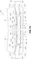
- Figure 14 shows a delamination occurring between the top oxidized region 800 and the lead frame 301 and propagating only up to the interface (still designated by IF) between the top oxidized region 800 and the top coating region 312, without affecting the adhesion between the top coating region 312 and the die pad 310.
- the interface IF between the top oxidized region 800 and the part of the top coating region 312 adjacent (i.e., in direct contact) to the top oxidized region 800 is overlaid by the packaging region 25 and acts as stop point to the propagation of a delamination between the top oxidized region 800 and the lead frame 301. Therefore, such a delamination does not cause, as an example, the detachment of the packaging region 25 from the top coating region 312.
- the present lead frame represents a cost-effective solution which allows to reduce the occurrence, in packaged integrated electronic devices, of the delamination between the molded packaging region and the metallic coating regions of the lead frame.
- the lead frame may have a shape different from the ones previously shown.
Landscapes
- Lead Frames For Integrated Circuits (AREA)
- Structures Or Materials For Encapsulating Or Coating Semiconductor Devices Or Solid State Devices (AREA)
Abstract
Description
- The present invention relates to a lead frame for a package for a semiconductor device, as well as to a semiconductor device and to a process for manufacturing a semiconductor device.
- As is known, semiconductor devices, such as for example integrated circuits and MEMS devices, are englobed inside corresponding packages, which perform functions of protection and interfacing with the outside world. For example, packages are known that enable so-called "surface mounting" on a printed-circuit board.
- In greater detail, surface-mount packages include, for example, the so-called packages of a "quad-flat no-leads" (QFN) type, also known as "micro lead frame" (MLF) packages or "small-outline no-leads" (SON) packages.
- In general, a QFN package comprises a region of resin, englobed inside which is a metallic lead frame (typically, made up of copper), which in turn forms at least one array of terminals that give out onto a bottom surface of the package.
- As shown in
Figures 1 and2 , a lead frame 1 includes amain body 2, which is planar and has, in top plan view, a polygonal shape (typically, a square or a rectangle); themain body 2 defines atop surface 6a and abottom surface 6b. A plurality ofpads 8 extend upwards from themain body 2, i.e. from thetop surface 6a. In addition, the lead frame 1 comprises the so-calleddie pad 10, which extend upwards from themain body 2 and is surrounded, at distance, by theinner pads 8. - The
main body 2, thepads 8 and thedie pad 10 form one single piece of metal. In addition, thedie pad 10 is planar and has, in top plan view, a polygonal shape (typically, a square or a rectangle) . InFigure 1 , thedie pad 10 has the shape of a parallelepiped and its lateral walls 16 define four edges 11 (only three visible inFigure 1 ). - In addition, the lead frame 1 is plated, usually by means of silver or a metallic alloy (such as NiPdAu). In particular, the lead frame 1 undergoes a plating process (e.g., an electroplating) which allows to form a
top coating region 12 on thedie pad 10, and a plurality ofsecondary coating regions 14, each of which is arranged on acorresponding pad 8. As mentioned before, thetop coating region 12 and thesecondary coating region 14 are formed by silver or a metallic alloy, i.e. by a material which is less prone to oxidation (in particular, oxidation in air) than the material forming the lead frame 1 (i.e., by a material having a lower oxidation rate than the lead frame). In addition, thetop coating region 12 and thesecondary coating region 14 may have a thickness comprised in the range 3-9µm; thepads 8 and thedie pad 10 may have a thickness comprised in the range 3-4µm. - Traditionally, lead frames are manufactured in strips, which are subsequently used in the manufacturing processes. Furthermore, the manufacturing processes typically comprise a step of back-etching to remove the
main body 2 and separate thepads 8 from thedie pad 10. - In addition, the manufacturing processes typically include the steps of setting the die (not shown) on the
die pad 10, and then electrically connecting the conductive pads of the die tocorresponding pads 8 of the lead frame 1, by means ofwire bondings 24, as shown inFigure 3 . In order to set up thewire bondings 24, a thermal treatment is carried out, usually at a temperature of about 200°C, in air, and with a duration of about ten minutes; such a thermal treatment causes a controlled oxidation of the exposed parts of the lead frame 1, i.e. of the parts of the lead frame 1 not coated by thetop coating region 12, nor by thesecondary coating regions 14. Therefore, after the thermal treatment, anoxidized layer 27 extends on parts of the lead frame 1, as well as under the lead frame 1. - A
packaging region 25 is then formed, typically by means of moulding, on top of the lead frame 1 and the die. Thepackaging region 25, also known as "moulding compound", may be made of a thermosetting epoxy resin and extends in direct contact with part of thetop coating region 12, as well as with thesecondary coating regions 14 and with the oxidizedlayer 27. - According to a different example, shown in
Figure 4 , the lead frame 1 may include adie pad structure 28 including thedie pad 10, aground ring 29 which laterally surrounds thedie pad 10, and a trench T0 extending between thedie pad 10 and theground ring 29, so as to expose a corresponding portion of the underlyingmain body 2. Theground ring 29 extends upwards from themain body 2, has the same thickness as thedie pad 10 and has the shape of a squared frame; theground ring 29 forms a single piece with themain body 2, thedie pad 10 and thepads 8 Thepads 8 surround thedie pad structure 28. In addition, theground ring 29 is coated, at top, by an additional coating region 12' , which is made of the same material as thetop coating region 12 and has the same thickness as this latter. - Either
Figure 1 andFigure 4 show in dashed line the projection of the outline OT of a possible die on thetop coating region 12. - This having been said, the difference between the coefficients of thermal expansion (CTE) of the
packaging region 25 and the lead frame 1 may cause mechanical stresses, due to temperature changes which occur during the functioning of the electronic device implemented in the die. - In particular, referring as an example to
Figures 1 and2 , the Applicant has noticed that mechanical stresses are concentrated at the corners of thedie pad 10, where they may induce a local delamination (i.e., the detachment of portions of thetop coating region 12 from the packaging region 25), which may then propagate, causing cracks and affecting the device reliability over time, in particular when causing the exposure of the die to the external atmosphere. - In order to solve the problem of the delamination, several solutions have been proposed.
- In particular, a first solution envisages the use of additional adhesion promoter materials to be applied on the lead frame surface. Unfortunately, such a solution entails high costs.
- A second solution envisages the formation of holding structures (such as grooves or dimples) in the lead frame. However, such a solution, besides entailing a reduction of the available packaging space, has proved to be not effective in case of large packaging formats, where higher stresses occur.
- Finally, a third solution has been proposed, which envisages the use of a so-called rough lead frame, i.e. a lead frame which has undergone a chemical or mechanical process to render its surfaces rough. Unfortunately, also this solution entails high costs; furthermore, it negatively affects the die attach glue control, due to increase of substrate wettability, and the reliability of the wire bondings.
-
US 2016/0355655 discloses a packaged device comprising a lead frame and a plurality of capacitors, which are attached to surface portions of structures of the lead frame. -
JP H03 149865 - The aim of the present invention is thus to provide a lead frame for a semiconductor device that will solve at least in part the drawbacks of the known art.
- According to the present invention, a lead frame for a semiconductor device, a semiconductor device and a process for manufacturing a semiconductor device are provided, as defined in the appended claims.
- For a better understanding of the present invention, preferred embodiments thereof are now described, purely by way of non-limiting example and with reference to the attached drawings, wherein:
-
Figure 1 schematically shows a perspective view of a lead frame; -
Figure 2 schematically shows a cross-section of the lead frame shown inFigure 1 , taken along the line II-II shown inFigure 1 ; -
Figure 3 schematically shows a cross-section of a portion of a packaged device including the lead frame shown inFigures 1 and2 ; -
Figure 4 schematically shows a perspective view of a further lead frame; -
Figure 5 schematically shows a perspective view of the present lead frame; -
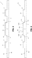
Figure 6 schematically shows a cross-section of the lead frame shown inFigure 5 , taken along the line VI-VI shown inFigure 5 ; -
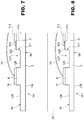
Figure 7 schematically shows a cross-section of a portion of a packaged device including the lead frame shown inFigures 5 and6 , during a step of a manufacturing process; -
Figure 8 schematically shows a cross-section of the packaged device shown inFigure 7 , during a following step of the manufacturing process; -
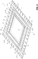
Figure 9 schematically shows a perspective view of a variant of the present lead frame; -
Figure 10 schematically shows a perspective view of a further variant of the present lead frame; -
Figure 11 schematically shows an enlarged perspective view of a portion of the lead frame shown inFigure 10 ; -
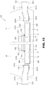
Figure 12 schematically shows an enlarged perspective view, taken from bottom, of a portion of the lead frame shown inFigures 10 and11 ; -
Figure 13 schematically shows a cross-section of a packaged device including the lead frame shown inFigures 10-12 , in a normal operative condition; and -
Figure 14 schematically shows a cross-section of the packaged device shown inFigure 13 , when delamination occurs. - The present lead frame stems from the idea of leaving exposed the corners of the die pad structure, so as to create sacrificial oxidized regions which allow to limit the delamination, as described here below, with reference to a lead frame of the type shown in
Figure 1 , without this implying any limitation. Therefore, the following description will limit to the differences over the lead frame 1 shown inFigure 1 ; in addition, the same reference signs will be used, unless stated otherwise. - In detail,
Figures 5 and6 show a lead frame (here designated by 101), in which the die pad (here designated by 110) has the same shape as thedie pad 10 ofFigures 1 and2 . In addition, the diepad 110 is delimited at top by afront surface 103. The top coating region (here designated by 112) extends on thefront surface 103, in direct contact. - In greater detail, the
top coating region 112 leaves exposed fourcorner portions 117 of thedie pad 110, which are delimited at top by corresponding portions of thetop surface 103, hereinafter referred to as the topangular surface portions 117S. - In particular, each
corner portion 117 includes a corresponding edge (here designated by 111) of thedie pad 110, perpendicular to thefront surface 103 and in contact with this latter. In addition, without this implying any limitation, the fourcorner portions 117 have one and the same shape; in particular, in top plan view, thecorner portions 117 have the shape of a square. Each topangular surface portion 117S extends from acorresponding edge 111 and is separate from the other topangular surface portions 117S; in top view, each topangular surface portion 117S extends from a corresponding vertex of the polygonal shape defined by thetop coating region 112. - In practice, the
top coating region 112 covers, in direct contact, thewhole front surface 103 of thedie pad 110, except the top angular surface portions 117S.During the manufacturing process, and in particular during the implementation of the wire bondings, the corresponding thermal treatment leads to the formation of a bottom oxidizedlayer 126, extending under thebottom surface 6b, and a top oxidizedlayer 127, as shown inFigure 7 . The bottom oxidizedlayer 126 and the top oxidizedlayer 127 may have a thickness comprised, as an example, in the range 100nm-200nm. - The top
oxidized region 127 includes amain portion 128, which extends on thetop surface 6a of themain body 2, as well as on the side walls of thepads 8 and thedie pad 110; therefore, themain portion 128 of the topoxidized region 127 coats theedges 111 of thedie pad 110. In addition, the topoxidized region 127 comprises four additional portions 129 (only one visible inFigure 7 ), hereinafter referred to as thesacrificial portions 129. - In particular, each
sacrificial portion 129 extends on acorresponding corner portion 117 of thedie pad 110, i.e. on a corresponding topangular surface portion 117S. In addition, eachsacrificial portion 129 is laterally staggered with respect to thetop coating region 112, with which it is in direct contact, thereby forming a corresponding interface IF. - Referring as an example to a following manufacturing step (shown in
Figure 8 ) of forming thepackaging region 25, such a step, per se known, includes a mold curing at (as an example) 170°C. Thepackaging region 25 extends, among other things, also on thesacrificial portions 129. - The abovementioned curing step causes mechanical stresses due to CTE (coefficient of thermal expansion) mismatch which are unlikely to cause a delamination between the
sacrificial portions 129 and thepackaging region 25, for the following reasons. - In detail, the Applicant has noticed that the adhesion between the top
oxidized region 127 and thepackaging region 25 is greater than the adhesion between the topoxidized region 127 and thelead frame 101. In greater detail, at each corner of thedie pad 110, the adhesion between the correspondingsacrificial portion 129 and the overlying portion of thepackaging region 25 is greater than the adhesion between thesacrificial portion 129 and theunderlying corner portion 117 of thedie pad 110. Therefore, delamination may occur, at most, between thesacrificial portions 129 and thedie pad 110; furthermore, such a delamination does not propagate beyond the interface IF between eachsacrificial portion 129 and thetop coating region 112, therefore it does not affect the adhesion between thepackaging region 25 and thetop coating region 112. Therefore, thepackaging region 25 and thetop coating region 112 continue to encapsulate the die, without exposing this latter to the external atmosphere. The reduced size of the topangular surface portion 117S with respect to thetop coating region 112 contributes to achieving this result. -
Figure 9 shows a further embodiment, which will be described hereinbelow with reference to the differences over the lead frame shown inFigure 4 . - In detail, referring to the additional front surface 103' to indicate the front surface of the
ground ring 29, the additional coating region 12' leaves exposed fourcorner portions 217 of theground ring 29, which are delimited at top by corresponding portions of the additional front surface 103', hereinafter referred to as the additional topangular surface portions 217S. In practice, the additional coating region 12' covers, in direct contact, the whole additional front surface 103', except the additional topangular surface portions 217S, which are separate from one another. - In particular, the
corner portions 217 of theground ring 29 include, each, acorresponding edge 211 of the lateral outer surface of the square frame forming theground ring 29. Furthermore, in top plan view, each topangular surface portion 217S has the shape of an "L". - During the manufacturing process, each additional top
angular surface portions 217S gets coated by a corresponding oxidized sacrificial region (not shown). Therefore, the embodiment shown inFigure 9 guarantees the same advantages as the one shown inFigures 6-8 . -
Figures 10-12 show a further embodiment, in which the lead frame, here designated by 301, is suitable to form a package of the so-called thin quad flat pack (TQFP) type. - In this case, the
lead frame 301 includes adie pad 310 with a squared planar shape, delimited at top and at bottom, respectively, by the front surface, here designated by 303 (visible inFigure 11 ), and by arear surface 405. The top coating region, here designated by 312, leaves exposed only the four top angular surface portions, here designated by 317S. Without this implying any limitation, the edges (here designated by 311) of thedie pad 310 are bevelled. Eachedge 311 is still formed by a corresponding pair of adjacent side walls (here designated by 316) of thedie pad 310. - In addition, the
rear surface 405 is coated, in direct contact, by abottom coating region 412, which is formed by the same material as the top coating region 312 (as an example, silver) and leaves exposed only fourcorner portions 417S of therear surface 405, hereinafter referred to as the bottomangular surface portions 417S. - Without this implying any limitation, a pair of (optional) trenches with concentric squared annular shapes may be present. In particular, a first and a second trench T1, T2 may extend through the
bottom coating region 412 and part of thedie pad 310, with a rectangular cross-section. In greater detail, the second trench T2 surrounds, at distance, the first trench T1; furthermore, the first and second trenches T1, T2 do not completely cross the die pad 310 (i.e., they are blind) and extend in such a way that, as shown inFigure 12 , each bottomangular surface portion 417S is divided into a first, a second and a thirdexposed subportion subportion 418A is arranged inwardly, whereas the third exposedsubportion 418C is arranged outwardly, towards the correspondingedge 311; the second exposedsubportion 418B is interposed between the first and the third exposed subportions 418A, 418C. - In addition, the
lead frame 310 comprises aninner frame 450 which is squared and planar and surrounds, at distance, thedie pad 310, to which it is connected by means of a plurality ofbridges 451. In particular, thedie pad 310, thebridges 451 and theinner frame 450 form one single piece of metal (i.e., they are made up of one and the same material); in addition, theinner frame 450 may be vertically staggered with respect to thedie pad 310, i.e. it may be arranged at an height (measured in a direction perpendicular to the die pad 310) higher than thedie pad 310. In addition, theinner frame 450 is delimited at top and at bottom by, respectively, atop frame surface 452 and abottom frame surface 453. - The
top coating region 312 extends also on the front surfaces of thebridges 451, as well as on the wholetop frame surface 452, with the exception of fourangular portions 457S of this latter, hereinafter referred to as the topframe surface portions 457S, which are thus left exposed. In top plan view, each topframe surface portions 457S has the shape of an "L", whose concavity houses part of the corresponding topangular surface portion 317S. - In addition, the
bottom coating region 412 extends also on the rear surfaces of thebridges 451, as well as on the wholebottom frame surface 453, with the exception of fourangular portions 467S of this latter, hereinafter referred to as the bottomframe surface portions 467S. In bottom view, each bottomframe surface portion 467S has the shape of an "L", whose concavity houses the corresponding third exposedsubportion 418C. Each bottomframe surface portion 467S and the corresponding topframe surface portion 457S delimit, respectively at top and at bottom, acorresponding corner portion 499 of theinner frame 450. - The
lead frame 301 further comprises anouter frame 470, which is planar and squared and surrounds, at distance, theinner frame 450, and a plurality of cantilever leads 472, eachcantilever lead 472 being fixed to theouter frame 470 and extending towards theinner frame 450. Without this implying any limitation, theouter frame 470 may be vertically staggered with respect to theinner frame 450, and in particular it may be arranged at an height higher than theinner frame 450. In this case, thedie pad 310, theinner frame 450 and theouter frame 470 lie in corresponding planes which, though arranged at different heights, are parallel. - In addition, the
lead frame 301 comprises four connectingelements 474, hereinafter referred to as tie bars 474. Eachtie bar 474 has an elongated shape and two ends, a first end being fixed to theinner frame 450, the second end being fixed to theouter frame 470. Thedie pad 310, theinner frame 450, theouter frame 470, the cantilever leads 472 and the tie bars 474 form a single metallic piece. - Each
tie bar 474 is delimited at top and at bottom by, respectively, a respectivetop surface 493 and arespective bottom surface 495. Furthermore, eachtie bar 474 comprises a slantedportion 475A and aplanar portion 475B. Theplanar portion 475B connects to theouter frame 470. The slantedportion 475A is interposed between theinner frame 450 and theplanar portion 475B; in particular, the slantedportion 475A connects to acorresponding corner portion 499 of theinner frame 450. In addition, either thetop surface 493 and thebottom surface 495 have the shape of a pair of plane surfaces connected to one another (i.e, one slanted plane surface and an horizontal plane surface, connected to one another). - In addition, the upper sides of the cantilever leads 472 and of the
outer frame 470 are coated by an outertop coating region 512; the lower sides of the cantilever leads 472 and of theouter frame 470 are coated by an outerbottom coating region 613. The outertop coating region 512 and the outerbottom coating region 613 may be formed by the same metallic material as thetop coating region 312 and thebottom coating region 412. - The outer
top coating region 512 leaves exposed aportion 517S of thetop surface 493 of eachtie bar 474, hereinafter referred to as the exposed top elongatedsurface 517S. Each exposed top elongatedsurface 517S connects to a corresponding topframe surface portion 457S. - The outer
bottom coating region 613 leaves exposed aportion 617S of thebottom surface 493 of eachtie bar 474, hereinafter referred to as the exposed bottom elongatedsurface 617S. Each exposed bottom elongatedsurface 617S connects to a corresponding bottomframe surface portion 467S. - As shown in
Figure 13 , thelead frame 301 may be used to manufacture an integratedelectronic device 700, which includes adie 502, fixed on a portion of thetop coating region 312 covering thedie pad 310, by means of an interposedlayer 503 of epoxy conductive glue, silver filled. Thepackaging region 25 englobes thelead frame 301, which has previously undergone a cutting process which, in a per se know manner, led to the removal of theouter frame 470, as well as of parts of the cantilever leads 472 and of the tie bars 474 connected thereto. - The
packaging region 25 leaves exposed thebottom coating region 412 and part of eachtie bar 474. In particular, for eachtie bar 474, outer parts of the exposed top elongatedsurface 517S and of the exposed bottom elongatedsurface 617S extend outside thepackaging region 25; inner parts of the exposed top elongatedsurface 517S and of the exposed bottom elongatedsurface 617S extend inside thepackaging region 25. - In addition, parts of the
tie bar 474 covered, on opposite sides, by the outertop coating region 512 and the outerbottom coating region 613 extend outside thepackaging region 25. - As previously explained, the exposed parts of the
lead frame 301 are covered by a metal oxide layer. In particular, each exposed top elongatedsurface 517S and the corresponding topframe surface portion 457S are coated by a corresponding topoxidized region 800; each exposed bottom elongatedsurface 617S and the corresponding bottomframe surface portion 467S are coated by a bottom oxidizedregion 802, forming one single oxidized region with the topoxidized region 800. - The Applicant has noticed that delamination is more likely to occur between the top/bottom oxidized
region 800/802 and thelead frame 301, than between the top/bottom oxidizedregion 800/802 and thepackaging region 25. As an example,Figure 14 shows a delamination occurring between the topoxidized region 800 and thelead frame 301 and propagating only up to the interface (still designated by IF) between the topoxidized region 800 and thetop coating region 312, without affecting the adhesion between thetop coating region 312 and thedie pad 310. - In greater detail, the interface IF between the top
oxidized region 800 and the part of thetop coating region 312 adjacent (i.e., in direct contact) to the topoxidized region 800 is overlaid by thepackaging region 25 and acts as stop point to the propagation of a delamination between the topoxidized region 800 and thelead frame 301. Therefore, such a delamination does not cause, as an example, the detachment of thepackaging region 25 from thetop coating region 312. - From what has been described and illustrated previously, the advantages that the present solution affords emerge clearly.
- In particular, the present lead frame represents a cost-effective solution which allows to reduce the occurrence, in packaged integrated electronic devices, of the delamination between the molded packaging region and the metallic coating regions of the lead frame.
- In conclusion, it is clear that modifications and variations may be made to what has been described and illustrated so far, without thereby departing from the scope of the present invention, as defined in the annexed claims.
- For example, the lead frame may have a shape different from the ones previously shown.
- Furthermore, variants are possible, which are the same as the one of
Figures 10-12 , but in which the die pad does not have any exposed surface portion and/or in which the exposed surface portions are arranged only on one side of the lead frame.
Claims (12)
- A lead frame for an integrated electronic device (700), comprising:- a die pad structure (110; 29,110; 310,450) of a first metallic material, including a die pad (110;310,450) and delimited by a top structure surface (103; 103,103'; 303, 452); and- a top coating structure (112; 12',112; 312, 512) formed by a second metallic material and arranged, in direct contact, on the top structure surface, the second material having an oxidation rate lower than the first material;
wherein the top coating structure leaves exposed a number of corner portions (117S; 217S; 457S) of the top structure surface, which are separate from one another. - The lead frame according to claim 1, wherein the die pad structure (110; 29,110; 310,450) forms a number of edges (11; 111); and wherein each edge is transversal to a corresponding corner portion (117S; 217S; 457S), with which it is in direct contact.
- The lead frame according to claim 1 or 2, wherein the top coating structure (112; 12',112; 312, 512) includes a top coating region (112) covering the die pad (110); and wherein said corner portions (117S) are formed by the die pad, which has a squared shape.
- The lead frame according to claim 1 or 2, wherein the die pad structure (29,110) further includes a ground ring (29) laterally surrounding the die pad (110) and having the shape of a squared frame; and wherein the top coating structure (112; 12',112; 312, 512) includes an additional top coating layer (12') covering the ground ring (29); and wherein said corner portions (217S) are formed by the ground ring.
- The lead frame according to claims 3 or 4, further including:- a main body (2); and- a plurality of pads (8), which form a single piece with the die pad (110) and the main body, the die pad and the pads extending from the main body, the pads being laterally staggered with respect to the die pad;
wherein the die pads are coated at top by corresponding top coating regions (14) of the second metallic material. - The lead frame according to claim 1, wherein the die pad structure (310,450) further includes an inner frame (450), which laterally surrounds the die pad (310); the lead frame (301) further including:- an outer frame (470), which laterally surrounds the inner frame; and- a number of tie bars (474), interposed between the outer frame and the inner frame;and wherein the top coating structure (312,512) includes:- a top coating region (312) covering the die pad and the inner frame;- an outer top coating region (512), covering the outer frame;
and wherein said corner portions (457S) are formed by the inner frame and connect to corresponding tie bars. - The lead frame according to claim 6, wherein the top coating region (312) and the outer top coating region (512) leave exposed the tie bars (474).
- The lead frame according to claim 6 or 7, wherein the inner frame (450) and the outer frame (470) are arranged at different heights, and wherein each tie bar (474) includes a corresponding slanted portion.
- The lead frame according to any of claims from 6 to 8, wherein the die pad (310) is delimited by a top surface (303); and wherein the top coating region (312) extends on the top surface, leaving exposed corner portions (317S) of the top surface.
- The lead frame according to any of claims from 6 to 9, further comprising:- a bottom coating structure (412) extending under the die pad (310) and the inner frame (450); and- an outer bottom coating region (612) extending under the outer frame (470);
and wherein the die pad structure (410,450) is further delimited by a bottom structure surface (405,453); and wherein the bottom coating structure leaves exposed a number of corner portions (467S) of the bottom structure surface, which are formed by the inner frame and connect corresponding tie bars. - An integrated electronic device comprising:- a lead frame (101; 301) according to any of the preceding claims;- a number of oxidized regions (129; 800), each of which coats a corresponding corner portion (117S; 217S; 457S) of the top structure surface (103; 103,103'; 303, 452) and laterally contacts the top coating structure (112; 12',112; 312,512);- a die (502), arranged on top of the die pad (110;310); and- a dielectric packaging region (25), which covers, in direct contact, the die, the oxidized regions and parts of the top coating structure adjacent to the oxidized regions.
- A method for manufacturing an integrated electronic device (700), comprising the steps of:- fixing a die (502) to a lead frame (101; 301) according to any of the claims 1-10;- setting up wire bondings (24) between the die and the lead frame, said step of setting up wire bonding comprising carrying out a thermal treatment which causes the formation of a number of oxidized regions (129; 800), each of which coats a corresponding corner portion (117S; 217S; 457S) of the top structure surface (103; 103,103'; 303, 452) and laterally contacts the top coating structure (112; 12',112; 312,512); and then- forming a dielectric packaging region (25) so that it covers, in direct contact, the die, the oxidized regions and parts of the top coating structure adjacent to the oxidized regions.
Applications Claiming Priority (1)
| Application Number | Priority Date | Filing Date | Title |
|---|---|---|---|
| IT201900013704 | 2019-08-01 |
Publications (2)
| Publication Number | Publication Date |
|---|---|
| EP3772097A1 true EP3772097A1 (en) | 2021-02-03 |
| EP3772097B1 EP3772097B1 (en) | 2022-09-28 |
Family
ID=68653545
Family Applications (1)
| Application Number | Title | Priority Date | Filing Date |
|---|---|---|---|
| EP20189128.0A Active EP3772097B1 (en) | 2019-08-01 | 2020-08-03 | Lead frame for a package for a semiconductor device, semiconductor device and process for manufacturing a semiconductor device |
Country Status (3)
| Country | Link |
|---|---|
| US (3) | US11515240B2 (en) |
| EP (1) | EP3772097B1 (en) |
| CN (2) | CN112310028B (en) |
Families Citing this family (2)
| Publication number | Priority date | Publication date | Assignee | Title |
|---|---|---|---|---|
| US11515240B2 (en) * | 2019-08-01 | 2022-11-29 | Stmicroelectronics S.R.L. | Lead frame for a package for a semiconductor device, semiconductor device and process for manufacturing a semiconductor device |
| CN114203663B (en) * | 2021-11-24 | 2022-08-19 | 广东气派科技有限公司 | Connecting rib structure of lead frame |
Citations (7)
| Publication number | Priority date | Publication date | Assignee | Title |
|---|---|---|---|---|
| JPH03149865A (en) | 1989-11-07 | 1991-06-26 | Matsushita Electron Corp | Lead frame |
| US20030075792A1 (en) * | 2001-09-28 | 2003-04-24 | Christian Ruhland | Electronic devices with semiconductor chips and a leadframe with device positions and methods for producing the same |
| EP1662565A2 (en) * | 2000-09-04 | 2006-05-31 | Dainippon Printing Co., Ltd. | Semiconductor package |
| WO2007011767A1 (en) * | 2005-07-18 | 2007-01-25 | Qualcomm Incorporated | Integrated circuit packaging |
| US20160035655A1 (en) * | 2014-07-28 | 2016-02-04 | Texas Instruments Incorporated | Semiconductor Package Having Etched Foil Capacitor Integrated Into Leadframe |
| US20160355655A1 (en) | 2015-06-05 | 2016-12-08 | Exxonmobil Chemical Patents Inc. | Bimodal Propylene Polymers and Sequential Polymerization |
| US20190221502A1 (en) * | 2018-01-17 | 2019-07-18 | Microchip Technology Incorporated | Down Bond in Semiconductor Devices |
Family Cites Families (7)
| Publication number | Priority date | Publication date | Assignee | Title |
|---|---|---|---|---|
| KR960006970B1 (en) * | 1993-05-03 | 1996-05-25 | 삼성전자주식회사 | Film Carrier and Manufacturing Method Thereof |
| US5695810A (en) * | 1996-11-20 | 1997-12-09 | Cornell Research Foundation, Inc. | Use of cobalt tungsten phosphide as a barrier material for copper metallization |
| TW200733272A (en) * | 2005-11-01 | 2007-09-01 | Koninkl Philips Electronics Nv | Methods of packaging a semiconductor die and die package formed by the methods |
| TWI405307B (en) * | 2009-09-18 | 2013-08-11 | 聯詠科技股份有限公司 | Chip package and its process |
| CN105097749B (en) * | 2014-04-15 | 2019-01-08 | 恩智浦美国有限公司 | Combined QFN and QFP semiconductor packages |
| EP2966677A1 (en) * | 2014-07-07 | 2016-01-13 | Nxp B.V. | Method of attaching electronic components by soldering with removal of substrate oxide coating using a flux, corresponding substrate and corresponding flip-chip component |
| US11515240B2 (en) * | 2019-08-01 | 2022-11-29 | Stmicroelectronics S.R.L. | Lead frame for a package for a semiconductor device, semiconductor device and process for manufacturing a semiconductor device |
-
2020
- 2020-07-28 US US16/940,815 patent/US11515240B2/en active Active
- 2020-07-31 CN CN202010757285.9A patent/CN112310028B/en active Active
- 2020-07-31 CN CN202021559770.7U patent/CN212907720U/en active Active
- 2020-08-03 EP EP20189128.0A patent/EP3772097B1/en active Active
-
2022
- 2022-11-28 US US18/070,051 patent/US12142552B2/en active Active
-
2024
- 2024-11-11 US US18/943,461 patent/US20250070000A1/en active Pending
Patent Citations (7)
| Publication number | Priority date | Publication date | Assignee | Title |
|---|---|---|---|---|
| JPH03149865A (en) | 1989-11-07 | 1991-06-26 | Matsushita Electron Corp | Lead frame |
| EP1662565A2 (en) * | 2000-09-04 | 2006-05-31 | Dainippon Printing Co., Ltd. | Semiconductor package |
| US20030075792A1 (en) * | 2001-09-28 | 2003-04-24 | Christian Ruhland | Electronic devices with semiconductor chips and a leadframe with device positions and methods for producing the same |
| WO2007011767A1 (en) * | 2005-07-18 | 2007-01-25 | Qualcomm Incorporated | Integrated circuit packaging |
| US20160035655A1 (en) * | 2014-07-28 | 2016-02-04 | Texas Instruments Incorporated | Semiconductor Package Having Etched Foil Capacitor Integrated Into Leadframe |
| US20160355655A1 (en) | 2015-06-05 | 2016-12-08 | Exxonmobil Chemical Patents Inc. | Bimodal Propylene Polymers and Sequential Polymerization |
| US20190221502A1 (en) * | 2018-01-17 | 2019-07-18 | Microchip Technology Incorporated | Down Bond in Semiconductor Devices |
Also Published As
| Publication number | Publication date |
|---|---|
| US20250070000A1 (en) | 2025-02-27 |
| US20210035894A1 (en) | 2021-02-04 |
| EP3772097B1 (en) | 2022-09-28 |
| CN112310028B (en) | 2026-01-27 |
| US11515240B2 (en) | 2022-11-29 |
| US12142552B2 (en) | 2024-11-12 |
| US20230090848A1 (en) | 2023-03-23 |
| CN212907720U (en) | 2021-04-06 |
| CN112310028A (en) | 2021-02-02 |
Similar Documents
| Publication | Publication Date | Title |
|---|---|---|
| US6410979B2 (en) | Ball-grid-array semiconductor device with protruding terminals | |
| US20250070000A1 (en) | Lead frame for a package for a semiconductor device, semiconductor device and process for manufacturing a semiconductor device | |
| US6437429B1 (en) | Semiconductor package with metal pads | |
| US8184453B1 (en) | Increased capacity semiconductor package | |
| US7804159B2 (en) | Semiconductor device and a method of manufacturing the same and a mounting structure of a semiconductor device | |
| EP3440697B1 (en) | Flat no-leads package with improved contact leads | |
| JP2957168B2 (en) | Lead frame and semiconductor package using the same | |
| US20120126378A1 (en) | Semiconductor device package with electromagnetic shielding | |
| TWI654729B (en) | Semiconductor device and method of manufacturing same | |
| KR20010022928A (en) | Plastic integrated circuit package and method and leadframe for making the package | |
| JP2005057067A (en) | Semiconductor device and manufacturing method thereof | |
| JP2002076228A (en) | Resin-sealed semiconductor device | |
| CN205194694U (en) | Surface mounting electron device | |
| KR20040037575A (en) | Micro leadless package having oblique etching line | |
| JPS60189940A (en) | Manufacture of resin seal type semiconductor device | |
| JP7223347B2 (en) | Manufacturing method of lead frame and semiconductor device | |
| TWI627714B (en) | Lead frame and chip package | |
| KR100871379B1 (en) | Manufacturing method of semiconductor package | |
| JP3424184B2 (en) | Resin-sealed semiconductor device | |
| KR100221918B1 (en) | Chip scale package | |
| JP4569048B2 (en) | Surface mount semiconductor package and manufacturing method thereof | |
| JP2002026168A (en) | Semiconductor device and method of manufacturing the same | |
| KR100800159B1 (en) | Semiconductor package and manufacturing method | |
| KR100201389B1 (en) | Semiconductor package | |
| KR100244254B1 (en) | Lead frame and semiconductor package with such lead frame |
Legal Events
| Date | Code | Title | Description |
|---|---|---|---|
| PUAI | Public reference made under article 153(3) epc to a published international application that has entered the european phase |
Free format text: ORIGINAL CODE: 0009012 |
|
| STAA | Information on the status of an ep patent application or granted ep patent |
Free format text: STATUS: THE APPLICATION HAS BEEN PUBLISHED |
|
| AK | Designated contracting states |
Kind code of ref document: A1 Designated state(s): AL AT BE BG CH CY CZ DE DK EE ES FI FR GB GR HR HU IE IS IT LI LT LU LV MC MK MT NL NO PL PT RO RS SE SI SK SM TR |
|
| AX | Request for extension of the european patent |
Extension state: BA ME |
|
| STAA | Information on the status of an ep patent application or granted ep patent |
Free format text: STATUS: REQUEST FOR EXAMINATION WAS MADE |
|
| 17P | Request for examination filed |
Effective date: 20210728 |
|
| RBV | Designated contracting states (corrected) |
Designated state(s): AL AT BE BG CH CY CZ DE DK EE ES FI FR GB GR HR HU IE IS IT LI LT LU LV MC MK MT NL NO PL PT RO RS SE SI SK SM TR |
|
| GRAP | Despatch of communication of intention to grant a patent |
Free format text: ORIGINAL CODE: EPIDOSNIGR1 |
|
| STAA | Information on the status of an ep patent application or granted ep patent |
Free format text: STATUS: GRANT OF PATENT IS INTENDED |
|
| INTG | Intention to grant announced |
Effective date: 20220330 |
|
| GRAS | Grant fee paid |
Free format text: ORIGINAL CODE: EPIDOSNIGR3 |
|
| GRAA | (expected) grant |
Free format text: ORIGINAL CODE: 0009210 |
|
| STAA | Information on the status of an ep patent application or granted ep patent |
Free format text: STATUS: THE PATENT HAS BEEN GRANTED |
|
| AK | Designated contracting states |
Kind code of ref document: B1 Designated state(s): AL AT BE BG CH CY CZ DE DK EE ES FI FR GB GR HR HU IE IS IT LI LT LU LV MC MK MT NL NO PL PT RO RS SE SI SK SM TR |
|
| REG | Reference to a national code |
Ref country code: GB Ref legal event code: FG4D |
|
| REG | Reference to a national code |
Ref country code: CH Ref legal event code: EP |
|
| REG | Reference to a national code |
Ref country code: AT Ref legal event code: REF Ref document number: 1521807 Country of ref document: AT Kind code of ref document: T Effective date: 20221015 |
|
| REG | Reference to a national code |
Ref country code: DE Ref legal event code: R096 Ref document number: 602020005320 Country of ref document: DE |
|
| REG | Reference to a national code |
Ref country code: IE Ref legal event code: FG4D |
|
| REG | Reference to a national code |
Ref country code: LT Ref legal event code: MG9D |
|
| PG25 | Lapsed in a contracting state [announced via postgrant information from national office to epo] |
Ref country code: SE Free format text: LAPSE BECAUSE OF FAILURE TO SUBMIT A TRANSLATION OF THE DESCRIPTION OR TO PAY THE FEE WITHIN THE PRESCRIBED TIME-LIMIT Effective date: 20220928 Ref country code: RS Free format text: LAPSE BECAUSE OF FAILURE TO SUBMIT A TRANSLATION OF THE DESCRIPTION OR TO PAY THE FEE WITHIN THE PRESCRIBED TIME-LIMIT Effective date: 20220928 Ref country code: NO Free format text: LAPSE BECAUSE OF FAILURE TO SUBMIT A TRANSLATION OF THE DESCRIPTION OR TO PAY THE FEE WITHIN THE PRESCRIBED TIME-LIMIT Effective date: 20221228 Ref country code: LV Free format text: LAPSE BECAUSE OF FAILURE TO SUBMIT A TRANSLATION OF THE DESCRIPTION OR TO PAY THE FEE WITHIN THE PRESCRIBED TIME-LIMIT Effective date: 20220928 Ref country code: LT Free format text: LAPSE BECAUSE OF FAILURE TO SUBMIT A TRANSLATION OF THE DESCRIPTION OR TO PAY THE FEE WITHIN THE PRESCRIBED TIME-LIMIT Effective date: 20220928 Ref country code: FI Free format text: LAPSE BECAUSE OF FAILURE TO SUBMIT A TRANSLATION OF THE DESCRIPTION OR TO PAY THE FEE WITHIN THE PRESCRIBED TIME-LIMIT Effective date: 20220928 |
|
| REG | Reference to a national code |
Ref country code: NL Ref legal event code: MP Effective date: 20220928 |
|
| REG | Reference to a national code |
Ref country code: AT Ref legal event code: MK05 Ref document number: 1521807 Country of ref document: AT Kind code of ref document: T Effective date: 20220928 |
|
| PG25 | Lapsed in a contracting state [announced via postgrant information from national office to epo] |
Ref country code: HR Free format text: LAPSE BECAUSE OF FAILURE TO SUBMIT A TRANSLATION OF THE DESCRIPTION OR TO PAY THE FEE WITHIN THE PRESCRIBED TIME-LIMIT Effective date: 20220928 Ref country code: GR Free format text: LAPSE BECAUSE OF FAILURE TO SUBMIT A TRANSLATION OF THE DESCRIPTION OR TO PAY THE FEE WITHIN THE PRESCRIBED TIME-LIMIT Effective date: 20221229 |
|
| PG25 | Lapsed in a contracting state [announced via postgrant information from national office to epo] |
Ref country code: SM Free format text: LAPSE BECAUSE OF FAILURE TO SUBMIT A TRANSLATION OF THE DESCRIPTION OR TO PAY THE FEE WITHIN THE PRESCRIBED TIME-LIMIT Effective date: 20220928 Ref country code: RO Free format text: LAPSE BECAUSE OF FAILURE TO SUBMIT A TRANSLATION OF THE DESCRIPTION OR TO PAY THE FEE WITHIN THE PRESCRIBED TIME-LIMIT Effective date: 20220928 Ref country code: PT Free format text: LAPSE BECAUSE OF FAILURE TO SUBMIT A TRANSLATION OF THE DESCRIPTION OR TO PAY THE FEE WITHIN THE PRESCRIBED TIME-LIMIT Effective date: 20230130 Ref country code: ES Free format text: LAPSE BECAUSE OF FAILURE TO SUBMIT A TRANSLATION OF THE DESCRIPTION OR TO PAY THE FEE WITHIN THE PRESCRIBED TIME-LIMIT Effective date: 20220928 Ref country code: CZ Free format text: LAPSE BECAUSE OF FAILURE TO SUBMIT A TRANSLATION OF THE DESCRIPTION OR TO PAY THE FEE WITHIN THE PRESCRIBED TIME-LIMIT Effective date: 20220928 Ref country code: AT Free format text: LAPSE BECAUSE OF FAILURE TO SUBMIT A TRANSLATION OF THE DESCRIPTION OR TO PAY THE FEE WITHIN THE PRESCRIBED TIME-LIMIT Effective date: 20220928 |
|
| PG25 | Lapsed in a contracting state [announced via postgrant information from national office to epo] |
Ref country code: SK Free format text: LAPSE BECAUSE OF FAILURE TO SUBMIT A TRANSLATION OF THE DESCRIPTION OR TO PAY THE FEE WITHIN THE PRESCRIBED TIME-LIMIT Effective date: 20220928 Ref country code: PL Free format text: LAPSE BECAUSE OF FAILURE TO SUBMIT A TRANSLATION OF THE DESCRIPTION OR TO PAY THE FEE WITHIN THE PRESCRIBED TIME-LIMIT Effective date: 20220928 Ref country code: IS Free format text: LAPSE BECAUSE OF FAILURE TO SUBMIT A TRANSLATION OF THE DESCRIPTION OR TO PAY THE FEE WITHIN THE PRESCRIBED TIME-LIMIT Effective date: 20230128 Ref country code: EE Free format text: LAPSE BECAUSE OF FAILURE TO SUBMIT A TRANSLATION OF THE DESCRIPTION OR TO PAY THE FEE WITHIN THE PRESCRIBED TIME-LIMIT Effective date: 20220928 |
|
| REG | Reference to a national code |
Ref country code: DE Ref legal event code: R097 Ref document number: 602020005320 Country of ref document: DE |
|
| PG25 | Lapsed in a contracting state [announced via postgrant information from national office to epo] |
Ref country code: NL Free format text: LAPSE BECAUSE OF FAILURE TO SUBMIT A TRANSLATION OF THE DESCRIPTION OR TO PAY THE FEE WITHIN THE PRESCRIBED TIME-LIMIT Effective date: 20220928 Ref country code: AL Free format text: LAPSE BECAUSE OF FAILURE TO SUBMIT A TRANSLATION OF THE DESCRIPTION OR TO PAY THE FEE WITHIN THE PRESCRIBED TIME-LIMIT Effective date: 20220928 |
|
| PG25 | Lapsed in a contracting state [announced via postgrant information from national office to epo] |
Ref country code: DK Free format text: LAPSE BECAUSE OF FAILURE TO SUBMIT A TRANSLATION OF THE DESCRIPTION OR TO PAY THE FEE WITHIN THE PRESCRIBED TIME-LIMIT Effective date: 20220928 |
|
| PLBE | No opposition filed within time limit |
Free format text: ORIGINAL CODE: 0009261 |
|
| STAA | Information on the status of an ep patent application or granted ep patent |
Free format text: STATUS: NO OPPOSITION FILED WITHIN TIME LIMIT |
|
| 26N | No opposition filed |
Effective date: 20230629 |
|
| PG25 | Lapsed in a contracting state [announced via postgrant information from national office to epo] |
Ref country code: SI Free format text: LAPSE BECAUSE OF FAILURE TO SUBMIT A TRANSLATION OF THE DESCRIPTION OR TO PAY THE FEE WITHIN THE PRESCRIBED TIME-LIMIT Effective date: 20220928 |
|
| PG25 | Lapsed in a contracting state [announced via postgrant information from national office to epo] |
Ref country code: MC Free format text: LAPSE BECAUSE OF FAILURE TO SUBMIT A TRANSLATION OF THE DESCRIPTION OR TO PAY THE FEE WITHIN THE PRESCRIBED TIME-LIMIT Effective date: 20220928 |
|
| REG | Reference to a national code |
Ref country code: CH Ref legal event code: PL |
|
| PG25 | Lapsed in a contracting state [announced via postgrant information from national office to epo] |
Ref country code: MC Free format text: LAPSE BECAUSE OF FAILURE TO SUBMIT A TRANSLATION OF THE DESCRIPTION OR TO PAY THE FEE WITHIN THE PRESCRIBED TIME-LIMIT Effective date: 20220928 |
|
| PG25 | Lapsed in a contracting state [announced via postgrant information from national office to epo] |
Ref country code: LU Free format text: LAPSE BECAUSE OF NON-PAYMENT OF DUE FEES Effective date: 20230803 |
|
| PG25 | Lapsed in a contracting state [announced via postgrant information from national office to epo] |
Ref country code: LU Free format text: LAPSE BECAUSE OF NON-PAYMENT OF DUE FEES Effective date: 20230803 Ref country code: CH Free format text: LAPSE BECAUSE OF NON-PAYMENT OF DUE FEES Effective date: 20230831 |
|
| REG | Reference to a national code |
Ref country code: BE Ref legal event code: MM Effective date: 20230831 |
|
| REG | Reference to a national code |
Ref country code: IE Ref legal event code: MM4A |
|
| PG25 | Lapsed in a contracting state [announced via postgrant information from national office to epo] |
Ref country code: IT Free format text: LAPSE BECAUSE OF FAILURE TO SUBMIT A TRANSLATION OF THE DESCRIPTION OR TO PAY THE FEE WITHIN THE PRESCRIBED TIME-LIMIT Effective date: 20220928 |
|
| PG25 | Lapsed in a contracting state [announced via postgrant information from national office to epo] |
Ref country code: IE Free format text: LAPSE BECAUSE OF NON-PAYMENT OF DUE FEES Effective date: 20230803 |
|
| PG25 | Lapsed in a contracting state [announced via postgrant information from national office to epo] |
Ref country code: IE Free format text: LAPSE BECAUSE OF NON-PAYMENT OF DUE FEES Effective date: 20230803 Ref country code: FR Free format text: LAPSE BECAUSE OF NON-PAYMENT OF DUE FEES Effective date: 20230831 |
|
| PG25 | Lapsed in a contracting state [announced via postgrant information from national office to epo] |
Ref country code: BE Free format text: LAPSE BECAUSE OF NON-PAYMENT OF DUE FEES Effective date: 20230831 |
|
| PG25 | Lapsed in a contracting state [announced via postgrant information from national office to epo] |
Ref country code: BG Free format text: LAPSE BECAUSE OF FAILURE TO SUBMIT A TRANSLATION OF THE DESCRIPTION OR TO PAY THE FEE WITHIN THE PRESCRIBED TIME-LIMIT Effective date: 20220928 |
|
| PG25 | Lapsed in a contracting state [announced via postgrant information from national office to epo] |
Ref country code: BG Free format text: LAPSE BECAUSE OF FAILURE TO SUBMIT A TRANSLATION OF THE DESCRIPTION OR TO PAY THE FEE WITHIN THE PRESCRIBED TIME-LIMIT Effective date: 20220928 |
|
| GBPC | Gb: european patent ceased through non-payment of renewal fee |
Effective date: 20240803 |
|
| PG25 | Lapsed in a contracting state [announced via postgrant information from national office to epo] |
Ref country code: GB Free format text: LAPSE BECAUSE OF NON-PAYMENT OF DUE FEES Effective date: 20240803 |
|
| PG25 | Lapsed in a contracting state [announced via postgrant information from national office to epo] |
Ref country code: CY Free format text: LAPSE BECAUSE OF FAILURE TO SUBMIT A TRANSLATION OF THE DESCRIPTION OR TO PAY THE FEE WITHIN THE PRESCRIBED TIME-LIMIT; INVALID AB INITIO Effective date: 20200803 |
|
| PG25 | Lapsed in a contracting state [announced via postgrant information from national office to epo] |
Ref country code: HU Free format text: LAPSE BECAUSE OF FAILURE TO SUBMIT A TRANSLATION OF THE DESCRIPTION OR TO PAY THE FEE WITHIN THE PRESCRIBED TIME-LIMIT; INVALID AB INITIO Effective date: 20200803 |
|
| PGFP | Annual fee paid to national office [announced via postgrant information from national office to epo] |
Ref country code: DE Payment date: 20250724 Year of fee payment: 6 |
|
| REG | Reference to a national code |
Ref country code: DE Ref legal event code: R079 Ref document number: 602020005320 Country of ref document: DE Free format text: PREVIOUS MAIN CLASS: H01L0023495000 Ipc: H10W0070400000 |
|
| PG25 | Lapsed in a contracting state [announced via postgrant information from national office to epo] |
Ref country code: TR Free format text: LAPSE BECAUSE OF FAILURE TO SUBMIT A TRANSLATION OF THE DESCRIPTION OR TO PAY THE FEE WITHIN THE PRESCRIBED TIME-LIMIT Effective date: 20220928 |