EP3771963A1 - Verfahren und vorrichtung zum ausgleichen von lasten und computerlesbares speichermedium - Google Patents
Verfahren und vorrichtung zum ausgleichen von lasten und computerlesbares speichermedium Download PDFInfo
- Publication number
- EP3771963A1 EP3771963A1 EP20165846.5A EP20165846A EP3771963A1 EP 3771963 A1 EP3771963 A1 EP 3771963A1 EP 20165846 A EP20165846 A EP 20165846A EP 3771963 A1 EP3771963 A1 EP 3771963A1
- Authority
- EP
- European Patent Office
- Prior art keywords
- data processing
- input data
- metric value
- clock cycle
- processing units
- Prior art date
- Legal status (The legal status is an assumption and is not a legal conclusion. Google has not performed a legal analysis and makes no representation as to the accuracy of the status listed.)
- Ceased
Links
Images



Classifications
-
- G—PHYSICS
- G06—COMPUTING OR CALCULATING; COUNTING
- G06F—ELECTRIC DIGITAL DATA PROCESSING
- G06F1/00—Details not covered by groups G06F3/00 - G06F13/00 and G06F21/00
- G06F1/26—Power supply means, e.g. regulation thereof
- G06F1/32—Means for saving power
- G06F1/3203—Power management, i.e. event-based initiation of a power-saving mode
- G06F1/3206—Monitoring of events, devices or parameters that trigger a change in power modality
-
- G—PHYSICS
- G06—COMPUTING OR CALCULATING; COUNTING
- G06F—ELECTRIC DIGITAL DATA PROCESSING
- G06F9/00—Arrangements for program control, e.g. control units
- G06F9/06—Arrangements for program control, e.g. control units using stored programs, i.e. using an internal store of processing equipment to receive or retain programs
- G06F9/46—Multiprogramming arrangements
- G06F9/50—Allocation of resources, e.g. of the central processing unit [CPU]
- G06F9/5094—Allocation of resources, e.g. of the central processing unit [CPU] where the allocation takes into account power or heat criteria
-
- G—PHYSICS
- G06—COMPUTING OR CALCULATING; COUNTING
- G06F—ELECTRIC DIGITAL DATA PROCESSING
- G06F9/00—Arrangements for program control, e.g. control units
- G06F9/06—Arrangements for program control, e.g. control units using stored programs, i.e. using an internal store of processing equipment to receive or retain programs
- G06F9/46—Multiprogramming arrangements
- G06F9/50—Allocation of resources, e.g. of the central processing unit [CPU]
- G06F9/5005—Allocation of resources, e.g. of the central processing unit [CPU] to service a request
- G06F9/5027—Allocation of resources, e.g. of the central processing unit [CPU] to service a request the resource being a machine, e.g. CPUs, Servers, Terminals
- G06F9/505—Allocation of resources, e.g. of the central processing unit [CPU] to service a request the resource being a machine, e.g. CPUs, Servers, Terminals considering the load
-
- G—PHYSICS
- G06—COMPUTING OR CALCULATING; COUNTING
- G06F—ELECTRIC DIGITAL DATA PROCESSING
- G06F1/00—Details not covered by groups G06F3/00 - G06F13/00 and G06F21/00
- G06F1/04—Generating or distributing clock signals or signals derived directly therefrom
- G06F1/08—Clock generators with changeable or programmable clock frequency
-
- G—PHYSICS
- G06—COMPUTING OR CALCULATING; COUNTING
- G06F—ELECTRIC DIGITAL DATA PROCESSING
- G06F1/00—Details not covered by groups G06F3/00 - G06F13/00 and G06F21/00
- G06F1/26—Power supply means, e.g. regulation thereof
- G06F1/32—Means for saving power
- G06F1/3203—Power management, i.e. event-based initiation of a power-saving mode
- G06F1/3234—Power saving characterised by the action undertaken
- G06F1/3243—Power saving in microcontroller unit
-
- G—PHYSICS
- G06—COMPUTING OR CALCULATING; COUNTING
- G06F—ELECTRIC DIGITAL DATA PROCESSING
- G06F1/00—Details not covered by groups G06F3/00 - G06F13/00 and G06F21/00
- G06F1/26—Power supply means, e.g. regulation thereof
- G06F1/32—Means for saving power
- G06F1/3203—Power management, i.e. event-based initiation of a power-saving mode
- G06F1/3234—Power saving characterised by the action undertaken
- G06F1/3287—Power saving characterised by the action undertaken by switching off individual functional units in the computer system
-
- G—PHYSICS
- G06—COMPUTING OR CALCULATING; COUNTING
- G06F—ELECTRIC DIGITAL DATA PROCESSING
- G06F9/00—Arrangements for program control, e.g. control units
- G06F9/06—Arrangements for program control, e.g. control units using stored programs, i.e. using an internal store of processing equipment to receive or retain programs
- G06F9/46—Multiprogramming arrangements
- G06F9/50—Allocation of resources, e.g. of the central processing unit [CPU]
- G06F9/5083—Techniques for rebalancing the load in a distributed system
-
- G—PHYSICS
- G06—COMPUTING OR CALCULATING; COUNTING
- G06F—ELECTRIC DIGITAL DATA PROCESSING
- G06F1/00—Details not covered by groups G06F3/00 - G06F13/00 and G06F21/00
- G06F1/26—Power supply means, e.g. regulation thereof
- G06F1/32—Means for saving power
- G06F1/3203—Power management, i.e. event-based initiation of a power-saving mode
- G06F1/3234—Power saving characterised by the action undertaken
- G06F1/3237—Power saving characterised by the action undertaken by disabling clock generation or distribution
-
- Y—GENERAL TAGGING OF NEW TECHNOLOGICAL DEVELOPMENTS; GENERAL TAGGING OF CROSS-SECTIONAL TECHNOLOGIES SPANNING OVER SEVERAL SECTIONS OF THE IPC; TECHNICAL SUBJECTS COVERED BY FORMER USPC CROSS-REFERENCE ART COLLECTIONS [XRACs] AND DIGESTS
- Y02—TECHNOLOGIES OR APPLICATIONS FOR MITIGATION OR ADAPTATION AGAINST CLIMATE CHANGE
- Y02D—CLIMATE CHANGE MITIGATION TECHNOLOGIES IN INFORMATION AND COMMUNICATION TECHNOLOGIES [ICT], I.E. INFORMATION AND COMMUNICATION TECHNOLOGIES AIMING AT THE REDUCTION OF THEIR OWN ENERGY USE
- Y02D10/00—Energy efficient computing, e.g. low power processors, power management or thermal management
Definitions
- Embodiments of the present disclosure relate to a field of computer, and more particularly to a method and apparatus for balancing loads, and a computer-readable storage medium.
- AI chips are dedicated to handle a large number of computing tasks in AI applications. Therefore, an AI chip is a kind of calculation-intensive chip, which has a strong computing power and a very large area.
- an AI chip is a kind of calculation-intensive chip, which has a strong computing power and a very large area.
- it very easy that hundreds of millions of transistors hop from idle state to active state at the same time and instantaneous power consumption of chips is extremely large, resulting in great challenges to power supply of chips at this moment. It is very easy to have a transient voltage drop, which leads to logic upset inside the entire chip and cannot work normally in serious cases.
- a large number of transistors hop from active state to idle state at the same time, it will occur an instantaneous voltage overshoot, which will also cause damage to power supply network.
- an improved solution for balancing loads to reduce instantaneous power consumption is provided.
- a method for balancing loads includes: for each data processing unit in a set of data processing units in a data processing system, acquiring current input data for the data processing unit in a current clock cycle and next input data for the data processing unit in a next clock cycle; and determining a first metric value indicating changes in input data of the data processing unit in the next clock cycle based on a comparison between the current input data and the next input data; and controlling an operating state of the set of data processing units in the next clock cycle based on the first metric value determined for the set of data processing units.
- acquiring the current input data and the next input data may include: selecting at least one set of input data from a plurality of sets of input data for the data processing unit; and acquiring the current input data and the next input data for each set of input data in the at least one set of input data respectively.
- the current input data is data at an output of an input data register for the data processing unit
- the next input data is data at an input of the input data register
- determining the first metric value may include: performing an exclusive-OR operation on corresponding bits of the current input data and next input data; and determining the first metric value based on a result of the exclusive-OR operation performed on the corresponding bits.
- controlling the operating state of the set of data processing units may include: determining a first total metric value indicating loads in the next clock cycle based on the first metric value of each data processing unit in the set of data processing units; in response to the first total metric value exceeding a first threshold, disabling at least a portion of the set of data processing units in the next clock cycle; and in response to the first total metric value smaller than the first threshold, enabling at least a portion of the set of data processing units in the next clock cycle.
- controlling the operating state of the set of data processing units may include: in response to the first metric value of a first data processing unit in the set of data processing units exceeding a second threshold, disabling the first data processing unit in the next clock cycle; and in response to the first metric value of the first data processing unit in the set of data processing units smaller than the second threshold, enabling the first data processing unit in the next clock cycle.
- controlling the operating state of the set of data processing units may include: determining a first total metric value for indicating loads in the next clock cycle based on the first metric value determined for the set of data processing units; determining a second total metric value for indicating loads in the current clock cycle based on previous input data in a previous clock cycle and the current input data in the current clock cycle of the set of data processing units; in response to an absolute value of a difference between the first total metric value and the second total metric value exceeding a third threshold, disabling at least a portion of the set of data processing units in the next clock cycle; and in response to the absolute value of the difference between the first total metric value and the second total metric value smaller than the third threshold, enabling at least a portion of the set of data processing units in the next clock cycle.
- determining the second total metric value may include: for each data processing unit in the set of data processing units, acquiring the previous input data in the previous clock cycle for the data processing unit; and determining a second metric value indicating changes in input data of the data processing unit in the current clock cycle based on a comparison between the previous input data and the current input data; and determining the second total metric value based on the second metric value determined for the set of data processing units.
- an apparatus for balancing loads includes: an acquiring unit, configured to acquire current input data for the data processing unit in a current clock cycle and next input data for the data processing unit in a next clock cycle, for each data processing unit in a set of data processing units in a data processing system; a determining unit, configured to determine a first metric value indicating changes in input data of the data processing unit in the next clock cycle based on a comparison between the current input data and the next input data for each data processing unit in the set of data processing units; and a control unit, configured to control an operating state of the set of data processing units in the next clock cycle based on the first metric value determined for the set of data processing units.
- the acquiring unit may include: a selecting unit, configured to select at least one set of input data from a plurality of sets of input data for the data processing unit; and an execution unit, configured to acquire the current input data and the next input data for each set of input data in the at least one set of input data respectively.
- the current input data is data at an output of an input data register for the data processing unit
- the next input data is data at an input of the input data register
- the determining unit may include: an exclusive-OR unit, configured to perform an exclusive-OR operation on corresponding bits of the current input data and next input data; and a first metric value determining unit, configured to determine the first metric value based on a result of the exclusive-OR operation performed on the corresponding bits.
- control unit may include: a first determining unit, configured to determine a first total metric value indicating loads in the next clock cycle based on the first metric value of each data processing unit in the set of data processing units; and a first disabling and enabling unit, configured to disable at least a portion of the set of data processing units in the next clock cycle in response to the first total metric value exceeding a first threshold, and enable at least a portion of the set of data processing units in the next clock cycle in response to the first total metric value smaller than the first threshold.
- control unit may include: a second disabling and enabling unit, configured to disable a first data processing unit in the next clock cycle in response to the first metric value of the first data processing unit in the set of data processing units exceeding a second threshold, and enable the first data processing unit in response to the first metric value of the first data processing unit in the set of data processing units smaller than the second threshold.
- a computer-readable storage medium having a computer program stored thereon which, when executed by a processor, implements a method for balancing loads according to embodiments of the present disclosure.
- Fig. 1 shows a schematic diagram of an example data processing system 100 in which embodiments of the present disclosure may be implemented.
- the data processing system 100 may be a system on chip.
- the data processing system 100 may be an AI chip.
- the data processing system 100 may be other chips except for an AI chip.
- embodiments of the present disclosure are in particular suitable to a chip with a large area and high power consumption for data processing.
- the data processing system 100 may include several data processing units 120. Although four data processing units 120 are shown in the figure, it should be understood that the number of data processing units 120 is not limited to this, but may be any number of more or less.
- these data processing units 120 may have the same data processing function.
- the data processing units 120 may each be a MAC unit for performing a multiply-adder (MAC) operation, and form a MAC unit array.
- these data processing units 120 may have different data processing functions.
- some data processing units 120 may be MAC units, while the other data processing units 120 may be units with other data processing functions except for performing MAC operations.
- MAC multiply-adder
- the data processing units 120 may be data processing units for implementing any suitable data processing functions known in the art or developed in the future, which is not limited in the present application.
- the impact on instantaneous high power consumption is mitigated by enhancing the power supply network and using more ultra-large capacitors inside the package and on the printed circuit board (PCB).
- PCB printed circuit board
- the costs for high-density capacitors are very expensive and affect final packaging and PCB size.
- it is impossible to increase capacitance indefinitely being subject to the limitations on packaging and PCB space. The simulation indicates that when the capacitance is increased to a certain degree, the problem of instantaneous high current cannot be further improved even if more capacitance is increased.
- a pulsation array is employed to achieve the effects of gradual initiation and gradual ending, thus reducing instantaneous high power consumption.
- the pulsating array may only effectively slow down instantaneous current at the initiating and ending times without avoiding instantaneous high current that occurs during the operation of chips. It also adds delay to the entire array.
- the inventor proposes to consider the controlling of instantaneous power consumption at the beginning of designing chips, and it automatically predicts and adjusts in advance instantaneous power consumption using a series of feedback mechanisms, thereby effectively controlling the changes in instantaneous voltage. Detailed description is made below in conjunction with Fig. 2 .
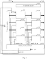
- Fig. 2 shows a schematic diagram 200 of a concept for balancing loads according to an embodiment of the present disclosure.
- the data processing units 120 may have a set of input data.
- the data processing units 120 may have two or more sets of input data.
- the data processing units 120 may acquire X input data and Y input data from X input data register 210 and Y input data unit 220, respectively.
- the acquisition for X input data is only shown in Fig. 2 .
- the statistical and control unit 230 may monitor changes in input data between the current clock cycle and next clock cycle of each data processing unit 120 (for example, as shown by toggle s0 ⁇ sn in Fig. 2 ), and determine the loads condition of the entire chip 100 in the next clock cycle according to the changes. Then, the operating state of each data processing unit 120 in the next clock cycle is controlled according to the loads condition. For example, by the clock control signal of gate_en and data flow control signal of flow_ctrl shown in Fig. 2 .
- gate en is shown herein only for one data processing unit 120, but in fact each data processing unit 120 may be controlled by gate_en.
- flow ctrl is shown herein only for X input data register 210, but in fact the operation of Y input data register 220 may also be controlled by flow ctrl. Thus the loads may be adjusted to reduce instantaneous high power consumption.
- the statistical and control unit 230 may be implemented in the form of software, hardware, firmware or any combination thereof. The following describes in more detail in conjunction with Fig. 3 to Fig. 7 .
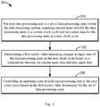
- Fig. 3 shows a flow chart of a method 300 for balancing loads according to an embodiment of the present disclosure.
- the method 300 may be implemented in any data processing system (e.g., the data processing system 100 of Fig. 1 ), for example, implemented at the statistical and control unit 230 of Fig. 2 .
- the set of data processing units 120 may be a part of data processing units 120 in the data processing system 100. In some alternative embodiments, the set of data processing units 120 may be all the data processing units 120 in the data processing system 100.
- At least one set of input data may be selected from multiple sets of input data (e.g., X input data and Y input data shown in Fig. 2 ) of the data processing units 120.
- the at least one set of input data may be randomly selected.
- the at least one set of input data may be selected as needed. Then, for each set of input data in the at least one set of input data, the acquisition operations of the current input data and next input data is executed respectively, that is, the current input data and the next input data for each set of input data in the at least one set of input data are acquired respectively.
- the current input data may be acquired at an output of input data register 210 or 220 for the data processing units 120, and the next input data may be acquired at an input of input data register 210 or 220. It should be understood that the current input data and next input data may also be obtained by any other suitable method, which is not particularly limited in this application.
- a first metric value indicating changes in input data of the data processing units 120 in the next clock cycle is determined based on a comparison between the current input data and the next input data.
- the current input data and next input data may be compared bit by bit to count bits flipping conditions.
- a flipped rate of bits may be determined as the first metric value.
- a non-flipped rate of bits may be determined as the first metric value. It should be understood that embodiments of the present disclosure are not limited to the above-mentioned counts of bits flipping conditions, and the first metric value may also be determined by any other suitable methods to indicate changes in input data of the data processing units in the next clock cycle.
- Fig. 4 shows a schematic diagram 400 of an exemplary implementation of the statistical and control unit 230 shown in Fig. 2 according to an embodiment of the present disclosure. As shown in Fig. 4 , determination of the flipped rate of bits may be implemented by module 420.
- the current input data for the data processing units 120 in the current clock cycle and the next input data for the data processing units 120 in the next clock cycle may be acquired by monitoring the output and input of X input data register 210, respectively.
- Exclusive OR operations are executed on n bits (in which, n is a positive integer) corresponding to the current input data and next input data, respectively, using exclusive OR (XOR) circuits 421-0 to 420-n.
- XOR exclusive OR
- n operation results of toggle _0 to toggle_n are obtained.
- n operation results of toggle_0 to toggle_n are summed by summation circuit (SUM) 422, thereby obtaining the flipped rate of bits toggle s of the data processing units 120 in the next clock cycle.
- SUM summation circuit
- the module 420 may be set for each data processing unit 120 to determine the corresponding flipped rate of bits (as shown by toggle_s0 ⁇ sn in Fig. 2 ). It should be understood that implementation of the module 420 shown in Fig. 4 is merely an example, and does not constitute any limitation to the present application. The determination of the flipped rate of bits may be implemented in any other suitable manner.
- the first metric value e.g., toggle_s0 ⁇ sn
- an operating state of each data processing unit 120 in the next clock cycle is controlled based on the first metric value determined for the set of data processing units 120. Therefore, the changes in input data of the data processing units 120 in the data processing system 100 may be dynamically controlled based on the actual data, thereby achieving the effects of dynamically balancing instantaneous large current and reducing instantaneous power consumption.
- Fig. 5 shows a flow chart of a method 500 for controlling an operating state of data processing units according to an embodiment of the present disclosure.
- the method 500 may be implemented at the statistical and control unit 230 of Fig. 2 .
- a first total metric value indicating loads in the next clock cycle may be determined based on the first metric value determined for the set of data processing units 120.
- the first total metric value may be determined by summing the first metric value corresponding to each data processing unit in the set of data processing units 120. For example, in a case where the first metric value is a flipped rate of bits, the first total metric value may be a total flipped rate of bits.
- weights may be determined for each data processing unit in the set of data processing units 120, and based on the weights, a weighted sum of the first metric values corresponding to each data processing unit in the set of data processing units 120 is performed, to determine the first total metric value.
- the weights may be determined according to functions of the data processing units.
- the weights may be determined according to the processing capabilities of data processing units. It should be understood that the weights may also be determined in any other suitable manner.
- a threshold may be set for the total metric value in this application scenario.
- the first threshold may be dynamically set.
- the first threshold may be configured by data processing system 100.
- the first threshold may be manually selected based on experiences.
- the first threshold may be predetermined.
- the at least a portion of the data processing units 120 may be randomly determined from the set of data processing units 120.
- the at least a portion of the data processing units 120 may be determined based on a comparison between the first metric value and a predetermined threshold (e.g., in a manner described below in combination with Fig. 6 ).
- the data processing units 120 may be enabled and disabled by a gating circuit.
- module 410 may be provided for each data processing unit 120.
- the module 410 may include a latch 411 and an "and" circuit (AND) 412.
- a gate signal of gate_en and an active-low clock (CLK) signal may be input to the latch 411.
- the input of the latch 411 is connected to one input of the AND 412, and the other input of the AND 412 receives a CLK signal.
- the output of the AND 412 is connected to X input data register 210 and Y input data register 220 for the data processing units 120.
- the statistical and control unit 230 may output a low-level gate en and a low-level flow_ctrl (as shown in Fig. 2 ).
- the output of AND 412 is a low level.
- X input data register 210 and Y input data register 220 are not operated, that is, data will not be supplied to data processing units 120 during this clock cycle, thereby the data processing units 120 being in a disabled state.
- data updates for X input data register 210 and Y input data register 220 are also suspended.
- the statistical and control unit 230 may output a high-level of gate_en and a high-level of flow_ctrl.
- the output of AND 412 is a high level.
- the data of X input data register 210 and Y input data register 220 are updated in this clock cycle, and X input data register 210 and Y input data register 220 supply the updated data to the data processing units 120 so that the data processing unit 120 is in an enabled state.
- the statistics and control of the metric value may be performed automatically in hardware, so the dynamic control speed is on a nanosecond level.
- the above-mentioned implementation described in conjunction with the module 410 shown in Fig. 4 is merely as an example, and the present application is not limited thereto, but it may be achieved in any other suitable manner that the control of operating state of data processing units.
- a control function of total power consumption may also be achieved at the same time.
- Fig. 6 shows a flow chart of a method 600 for controlling an operating state of data processing units according to another embodiment of the present disclosure.
- the method 600 may be implemented at the statistical and control unit 230 of Fig. 2 .
- operations are performed for each data processing unit in the set of data processing units 120.
- the second threshold may be dynamically set.
- the second threshold may be configured by the data processing system 100.
- the second threshold may be manually selected based on experiences.
- the second threshold may be predetermined.
- Fig. 7 shows a flow chart of a method 700 for controlling an operating state of data processing units according to another embodiment of the present disclosure.
- the method 700 may be implemented at the statistical and control unit 230 of Fig. 2 .
- a first total metric value indicating loads in the next clock cycle may be determined based on the first metric value determined for the set of data processing units 120.
- the processing at block 710 is similar to the processing described in conjunction with block 510 of Fig. 5 , which is not repeated herein again.
- a second total metric value for indicating loads in the current clock cycle may be determined based on previous input data in a previous clock cycle and current input data in a current clock cycle of the set of data processing units 120.
- previous input data in a previous clock cycle for the data processing unit may be acquired, and a second metric value indicating changes in input data of the data processing unit in the current clock cycle may be determined based on a comparison between the previous input data and current input data.
- a second total metric value is determined based on the second metric value determined for the set of data processing units.
- the determination method of the second total metric value is similar to the determination method of the first total metric value.
- Other details may refer to the related processing described in conjunction with block 510 of Fig. 5 , which is not repeated herein again.
- the third threshold may be dynamically set.
- the third threshold may be configured by data processing system 100.
- the third threshold may be manually selected based on experiences.
- the third threshold may be predetermined.
- the at least a portion of the data processing units 120 may be randomly determined from the set of data processing units 120.
- the at least a portion of the data processing units 120 may be determined based on a comparison between the first metric value with a predetermined threshold (e.g., in a manner described in conjunction with Fig. 6 ).
- a predetermined threshold e.g., in a manner described in conjunction with Fig. 6 .
- the implementation of disabling and enabling the data processing units is similar to the foregoing description in conjunction with Fig. 5 , which is not repeated herein again.
- multiple clock cycles may be selected to complete the control of data processing unit 120. By turning on different data processing units in different clock cycles, it may be achieved that instantaneous high current is distributed to multiple clock cycles. In addition, it may be dynamically adjusted according to actual needs, and the clock control signal of gate_en and the data flow control signal of flow ctrl are released after dynamic adjustments end, so as to restore to the normal mode.
- the manner of controlling loads according to embodiments of the present disclosure is very flexible, and loads may be dynamically and multi-dimensionally adjusted according to the actual situation, so as to meet the requirements of various application scenarios.
- the flipped rate of circuits is controlled in a simple gated clock manner, which solves the problem of instantaneous high current and high power consumption without increasing the costs of packaging and PCB.
- control logics required for the entire control is relatively small and the resulting increase in chips area is almost negligible.
- FIG. 8 shows a schematic block diagram of an apparatus 800 for balancing loads according to an embodiment of the present disclosure.
- the apparatus 800 may be implemented, for example, at the data processing system 100 of Fig. 1 .
- apparatus 800 may include an acquiring unit 810, a determining unit 820, and a control unit 830.
- acquiring unit 810 may be configured to acquire current input data for the data processing unit in a current clock cycle and next input data for the data processing unit in a next clock cycle, for each data processing unit in a set of data processing units (for example, the data processing units 120 of Fig. 1 ) within a data processing system (for example, the data processing system 100 of Fig. 1 ).
- the determining unit 820 may be configured to determine a first metric value indicating changes in input data of the data processing unit in the next clock cycle based on a comparison between the current input data and next input data for each data processing unit in the set of data processing units 120.
- the control unit 830 may be configured to control an operating state of the set of data processing units in the next clock cycle based on the first metric value determined for the set of data processing units.
- the acquiring unit 810 may include: a selecting unit, configured to select at least one set of input data from a plurality of sets of input data for the data processing unit; and an execution unit, configured to execute said acquiring respectively for each set of input data in the at least one set of input data.
- the current input data is one at an output of an input data register (e.g., X input data register 210 of Fig. 2 ) for the data processing unit, and the next input data is one at an input of the input data register.
- the determining unit 820 may include an exclusive-OR unit, configured to perform an exclusive-OR operation on corresponding bits of the current input data and next input data; and a first metric value determining unit, configured to determine the first metric value based on a result of the exclusive-OR operation of the corresponding bits.
- control unit 830 may include: a first determining unit, configured to determine a first total metric value indicating loads in the next clock cycle based on the first metric value of each data processing unit in the set of data processing units 120; and a first disabling and enabling unit, configured to disable at least a portion of the set of data processing units 120 in the next clock cycle in response to the first total metric value exceeding a first threshold, and enable at least a portion of the set of data processing units 120 in the next clock cycle in response to the first total metric value being below (i.e., smaller than) the first threshold.
- control unit 830 may include: a second disabling and enabling unit, configured to disable the data processing unit in the next clock cycle in response to the first metric value of the one data processing unit in the set of data processing units 120 exceeding a second threshold, and enable the data processing unit in response to the first metric value of the data processing unit in the set of data processing units being below the second threshold.
- control unit 830 may include: a first determining unit, configured to determine a first total metric value for indicating loads in the next clock cycle based on the first metric value determined for the set of data processing units 120; a second determining unit, configured to determine a second total metric value for indicating loads in the current clock cycle based on previous input data in a previous clock cycle and the current input data in the current clock cycle of the set of data processing units 120; and a third disabling and enabling unit, configured to disable at least a portion of the set of data processing units 120 in the next clock cycle in response to an absolute value of a difference between the first total metric value and the second total metric value exceeding a third threshold, and enable at least a portion of the set of data processing units 120 in response to an absolute value of a difference between the first total metric value and the second total metric value being below the third threshold value.
- the second determining unit includes: a data acquiring unit, configured to acquire the previous input data in the previous clock cycle for the data processing unit for each data processing unit in the set of data processing units 120; a second metric value determining unit, configured to determine a second metric value indicating changes in input data of the data processing unit in the current clock cycle based on a comparison between the previous input data and the current input data; a second total metric value determining unit, configured to determine the second total metric value based on the second metric value determined for the set of data processing units 120.
- each unit recorded in the apparatus 800 corresponds to each step in the methods of 300-700 described with reference to Fig. 2 to Fig. 7 , respectively.
- the apparatus 800 and the operations and features of the units included therein all correspond to the operations and features described above in conjunction with Fig. 2 to Fig. 7 , and have the same effect, of which the specific details are not repeated again.
- the units included in the apparatus 800 may be implemented in various ways, including software, hardware, firmware, or any combination thereof.
- one or more units may be implemented using software and/or firmware, e.g., machine-executable instructions stored on a storage medium.
- some or all of the units in the apparatus 800 may be implemented, at least in part, by one or more hardware logic components.
- exemplary types of hardware logic components include, without limitation: a field programmable gate array (FPGA), an application specific integrated circuit (ASIC), an application specific standard product (ASSP), a system on chip (SOC), a complex programmable logic devices (CPLD), and so on.
- Fig. 8 may be partially or entirely implemented as hardware modules, software modules, firmware modules, or any combination thereof.
- the processes, methods, or procedures described above may be implemented by hardware in a storage system or a host corresponding to the storage system or other computing devices independent of the storage system.
- Fig. 9 illustrates a schematic block diagram of an exemplary computing device 900 that may be used to implement embodiments of the present disclosure.
- the device 900 may be used to implement the data processing system 100 of Fig. 1 .
- the device 900 includes a central processing unit (CPU) 901, which may perform various appropriate actions and processes according to computer program instructions stored in a read only memory (ROM) 902 or computer program instructions loaded from a storage unit 908 into a random access memory (RAM) 903.
- ROM read only memory
- RAM random access memory
- various programs and data required for the operation of device 900 may also be stored.
- CPU 901, ROM 902, and RAM 903 are connected to each other through a bus 904.
- An input/output (I/O) interface 905 is also connected to the bus 904.
- a plurality of components in device 900 are connected to the I/O interface 905, including: an input unit 906, e.g., a keyboard, a mouse, etc.; an output unit 907, e.g., various types of displays, speakers, etc.; a storage unit 908, e.g., magnetic disks, an optical disks, etc.; and communication units 909, e.g. network cards, modems, wireless communication transceivers, etc.. Communication units 909 allow device 900 to exchange information/data with other devices through a computer network such as the Internet and/or various telecommunication networks.
- a computer network such as the Internet and/or various telecommunication networks.
- the processing unit 901 performs various methods and operations described above, such as the methods 300, 500, 600, and 700.
- the methods 300, 500, 600, and 700 may be implemented as computer software programs which are tangibly contained in a machine-readable medium, e.g., the storage unit 908.
- a part or all of the computer programs may be loaded and/or installed on the device 900 via the ROM 902 and/or the communication units 909.
- CPU 901 may be configured to perform the methods 300, 500, 600, and 700 in any other suitable manner (e.g., by means of firmware).
- Program codes for implementing methods of the present disclosure may be written in any combination of one or more programming languages. These program codes may be provided to a processor or controller of a general-purpose computer, special-purpose computer or other programmable data processing apparatus, so that program codes, when executed by the processor or controller, cause the functions/operations specified in the flow charts and/or block diagrams to be performed.
- the program codes may be executed entirely on a machine, partly on the machine, as a separate software package, partly on the machine, partly on a remote machine, or entirely on the remote machine or server.
- a machine-readable medium may be a tangible medium that may contain or store a program for use by or in connection with an instruction execution system, apparatus, or device.
- the machine-readable medium may be a machine-readable signal medium or a machine-readable storage medium.
- a machine-readable medium may include, but is not limited to, an electronic, magnetic, optical, electromagnetic, infrared, or semiconductor system, apparatus or device, or any suitable combination thereof.
- machine-readable storage media would include electrical connections based on one or more wires, a portable computer disk, a hard disk, a random access memory (RAM), a read-only memory (ROM), an erasable programmable read-only memory (EPROM) or a flash memory, an optical fiber, a compact disc read-only memory (CD-ROM), an optical storage device, a magnetic storage device, or any suitable combination thereof.
- RAM random access memory
- ROM read-only memory
- EPROM erasable programmable read-only memory
- flash memory an optical fiber
- CD-ROM compact disc read-only memory
- CD-ROM compact disc read-only memory
- magnetic storage device or any suitable combination thereof.
Landscapes
- Engineering & Computer Science (AREA)
- Theoretical Computer Science (AREA)
- General Engineering & Computer Science (AREA)
- Software Systems (AREA)
- Physics & Mathematics (AREA)
- General Physics & Mathematics (AREA)
- Computer Hardware Design (AREA)
- Computing Systems (AREA)
- Power Sources (AREA)
- Microcomputers (AREA)
- Advance Control (AREA)
- Multi Processors (AREA)
Applications Claiming Priority (1)
| Application Number | Priority Date | Filing Date | Title |
|---|---|---|---|
| CN201910690754.7A CN110413414B (zh) | 2019-07-29 | 2019-07-29 | 用于平衡负载的方法、装置、设备和计算机可读存储介质 |
Publications (1)
| Publication Number | Publication Date |
|---|---|
| EP3771963A1 true EP3771963A1 (de) | 2021-02-03 |
Family
ID=68363912
Family Applications (1)
| Application Number | Title | Priority Date | Filing Date |
|---|---|---|---|
| EP20165846.5A Ceased EP3771963A1 (de) | 2019-07-29 | 2020-03-26 | Verfahren und vorrichtung zum ausgleichen von lasten und computerlesbares speichermedium |
Country Status (5)
| Country | Link |
|---|---|
| US (1) | US11537441B2 (de) |
| EP (1) | EP3771963A1 (de) |
| JP (1) | JP7110278B2 (de) |
| KR (1) | KR102335749B1 (de) |
| CN (1) | CN110413414B (de) |
Families Citing this family (4)
| Publication number | Priority date | Publication date | Assignee | Title |
|---|---|---|---|---|
| EP3905565A4 (de) | 2018-12-29 | 2022-03-23 | Huawei Technologies Co., Ltd. | Vektoranzeigeverfahren zur erstellung eines vorcodierungsvektors und kommunikationsvorrichtung |
| CN111865744B (zh) * | 2020-07-08 | 2021-12-31 | 北京软安科技有限公司 | 一种车辆can总线数据分类方法及装置 |
| US11789518B2 (en) * | 2021-06-22 | 2023-10-17 | International Business Machines Corporation | Voltage overshoot management |
| US11592895B1 (en) * | 2021-06-30 | 2023-02-28 | Epirus, Inc. | Systems and methods for improving power efficiency |
Citations (8)
| Publication number | Priority date | Publication date | Assignee | Title |
|---|---|---|---|---|
| US5953237A (en) * | 1996-11-25 | 1999-09-14 | Hewlett-Packard Company | Power balancing to reduce step load |
| WO2004107144A1 (en) * | 2003-05-27 | 2004-12-09 | Koninklijke Philips Electronics N.V. | Monitoring and controlling power consumption |
| US20150089251A1 (en) * | 2013-09-26 | 2015-03-26 | Cavium, Inc. | Method and Apparatus for Managing Global Chip Power on a Multicore System on Chip |
| US20150220128A1 (en) * | 2014-02-04 | 2015-08-06 | Infineon Technologies Ag | Method and Apparatus for Use in a Data Processing System |
| GB2542215A (en) * | 2016-01-18 | 2017-03-15 | Imagination Tech Ltd | Dynamic power measurement using formal |
| US9735778B1 (en) * | 2014-08-20 | 2017-08-15 | Altera Corporation | Method and apparatuses for optimizing power management on an integrated circuit device |
| US20180329471A1 (en) * | 2017-05-10 | 2018-11-15 | Texas Instruments Incorporated | Fine-grained dynamic power and clock-gating control |
| US20190187775A1 (en) * | 2017-12-18 | 2019-06-20 | Facebook, Inc. | Dynamic power management for artificial intelligence hardware accelerators |
Family Cites Families (6)
| Publication number | Priority date | Publication date | Assignee | Title |
|---|---|---|---|---|
| US6822478B2 (en) * | 2001-07-03 | 2004-11-23 | Texas Instruments Incorporated | Data-driven clock gating for a sequential data-capture device |
| CN100403645C (zh) * | 2006-03-23 | 2008-07-16 | 湖南大学 | 数字化ups/eps空间矢量调制算法 |
| CN101499957B (zh) * | 2008-01-29 | 2011-06-15 | 中国电信股份有限公司 | 一种多径负载均衡的实现方法和数据转发装置 |
| US8954977B2 (en) * | 2008-12-09 | 2015-02-10 | Intel Corporation | Software-based thread remapping for power savings |
| US9167033B2 (en) * | 2013-03-14 | 2015-10-20 | Comcast Cable Holdings, Llc | Transmission device load balancing |
| CN108628693B (zh) * | 2018-04-17 | 2019-10-25 | 清华大学 | 处理器调试方法和系统 |
-
2019
- 2019-07-29 CN CN201910690754.7A patent/CN110413414B/zh active Active
-
2020
- 2020-03-26 EP EP20165846.5A patent/EP3771963A1/de not_active Ceased
- 2020-04-14 KR KR1020200045445A patent/KR102335749B1/ko active Active
- 2020-07-08 JP JP2020117637A patent/JP7110278B2/ja active Active
- 2020-07-15 US US16/929,970 patent/US11537441B2/en active Active
Patent Citations (8)
| Publication number | Priority date | Publication date | Assignee | Title |
|---|---|---|---|---|
| US5953237A (en) * | 1996-11-25 | 1999-09-14 | Hewlett-Packard Company | Power balancing to reduce step load |
| WO2004107144A1 (en) * | 2003-05-27 | 2004-12-09 | Koninklijke Philips Electronics N.V. | Monitoring and controlling power consumption |
| US20150089251A1 (en) * | 2013-09-26 | 2015-03-26 | Cavium, Inc. | Method and Apparatus for Managing Global Chip Power on a Multicore System on Chip |
| US20150220128A1 (en) * | 2014-02-04 | 2015-08-06 | Infineon Technologies Ag | Method and Apparatus for Use in a Data Processing System |
| US9735778B1 (en) * | 2014-08-20 | 2017-08-15 | Altera Corporation | Method and apparatuses for optimizing power management on an integrated circuit device |
| GB2542215A (en) * | 2016-01-18 | 2017-03-15 | Imagination Tech Ltd | Dynamic power measurement using formal |
| US20180329471A1 (en) * | 2017-05-10 | 2018-11-15 | Texas Instruments Incorporated | Fine-grained dynamic power and clock-gating control |
| US20190187775A1 (en) * | 2017-12-18 | 2019-06-20 | Facebook, Inc. | Dynamic power management for artificial intelligence hardware accelerators |
Also Published As
| Publication number | Publication date |
|---|---|
| US11537441B2 (en) | 2022-12-27 |
| JP2021022373A (ja) | 2021-02-18 |
| KR20210014063A (ko) | 2021-02-08 |
| CN110413414B (zh) | 2025-09-19 |
| CN110413414A (zh) | 2019-11-05 |
| KR102335749B1 (ko) | 2021-12-06 |
| JP7110278B2 (ja) | 2022-08-01 |
| US20210034421A1 (en) | 2021-02-04 |
Similar Documents
| Publication | Publication Date | Title |
|---|---|---|
| US11537441B2 (en) | Method and apparatus for balancing loads, and computer-readable storage medium | |
| US11520968B2 (en) | Verification platform for system on chip and verification method thereof | |
| EP3846036A1 (de) | Matrixspeicherverfahren, matrixzugriffsverfahren, einrichtung und elektronische vorrichtung | |
| US11442890B1 (en) | On-circuit data activity monitoring for a systolic array | |
| US10761583B2 (en) | Variation-aware intra-node power shifting among different hardware components | |
| CN106168993B (zh) | 电网实时仿真分析系统 | |
| KR20210151727A (ko) | 신경망 가속기의 데이터 처리 방법, 장치, 기기 및 저장 매체 | |
| US20230259737A1 (en) | Integrated computing apparatus, chip, board card, device and computing method | |
| JP7672405B2 (ja) | データセンタにおけるオーバクロックを管理する方法及び装置 | |
| CN116402149B (zh) | 一种量子线路优化方法、装置、存储介质及电子装置 | |
| CN117591378A (zh) | 一种服务器的温度控制方法、系统、设备及存储介质 | |
| CN114879832B (zh) | 用于运算装置的功耗控制方法、装置、芯片、设备及介质 | |
| CN114035795B (zh) | 核函数预编译方法、装置、计算机设备和存储介质 | |
| US20220206554A1 (en) | Processor and power supply ripple reduction method | |
| CN109949956A (zh) | 一种核电站控制系统高负荷工况模拟方法及系统 | |
| CN105824268B (zh) | 验证电源管理系统的方法及验证装置 | |
| US20210132671A1 (en) | Method and apparatus for selective fan control in an information handling system | |
| CN117234744B (zh) | 一种多芯片系统性能优化方法、系统、电子设备及介质 | |
| CN111966204A (zh) | 一种温度监控方法、电路、设备及存储介质 | |
| US11449337B1 (en) | Pseudorandom keephot instructions to mitigate large load steps during hardware emulation | |
| US12487880B2 (en) | Data check method and related device | |
| US20250077243A1 (en) | Randomization of instruction execution flow for glitch protection | |
| US20250292085A1 (en) | Model Training Method and Related Device | |
| US9886073B2 (en) | Control method for shared devices and electronic device | |
| CN116048227A (zh) | 一种基于fpga的多机复位方法、装置及介质 |
Legal Events
| Date | Code | Title | Description |
|---|---|---|---|
| PUAI | Public reference made under article 153(3) epc to a published international application that has entered the european phase |
Free format text: ORIGINAL CODE: 0009012 |
|
| STAA | Information on the status of an ep patent application or granted ep patent |
Free format text: STATUS: THE APPLICATION HAS BEEN PUBLISHED |
|
| AK | Designated contracting states |
Kind code of ref document: A1 Designated state(s): AL AT BE BG CH CY CZ DE DK EE ES FI FR GB GR HR HU IE IS IT LI LT LU LV MC MK MT NL NO PL PT RO RS SE SI SK SM TR |
|
| AX | Request for extension of the european patent |
Extension state: BA ME |
|
| STAA | Information on the status of an ep patent application or granted ep patent |
Free format text: STATUS: REQUEST FOR EXAMINATION WAS MADE |
|
| 17P | Request for examination filed |
Effective date: 20210802 |
|
| RBV | Designated contracting states (corrected) |
Designated state(s): AL AT BE BG CH CY CZ DE DK EE ES FI FR GB GR HR HU IE IS IT LI LT LU LV MC MK MT NL NO PL PT RO RS SE SI SK SM TR |
|
| RAP1 | Party data changed (applicant data changed or rights of an application transferred) |
Owner name: KUNLUNXIN TECHNOLOGY (BEIJING) COMPANY LIMITED |
|
| STAA | Information on the status of an ep patent application or granted ep patent |
Free format text: STATUS: THE APPLICATION HAS BEEN REFUSED |
|
| 18R | Application refused |
Effective date: 20230117 |