EP3771962A1 - Power sequencing in an active silicon interposer - Google Patents
Power sequencing in an active silicon interposer Download PDFInfo
- Publication number
- EP3771962A1 EP3771962A1 EP20188629.8A EP20188629A EP3771962A1 EP 3771962 A1 EP3771962 A1 EP 3771962A1 EP 20188629 A EP20188629 A EP 20188629A EP 3771962 A1 EP3771962 A1 EP 3771962A1
- Authority
- EP
- European Patent Office
- Prior art keywords
- power
- switch
- interposer
- control
- control input
- Prior art date
- Legal status (The legal status is an assumption and is not a legal conclusion. Google has not performed a legal analysis and makes no representation as to the accuracy of the status listed.)
- Granted
Links
Images


Classifications
-
- H—ELECTRICITY
- H03—ELECTRONIC CIRCUITRY
- H03K—PULSE TECHNIQUE
- H03K17/00—Electronic switching or gating, i.e. not by contact-making and –breaking
- H03K17/51—Electronic switching or gating, i.e. not by contact-making and –breaking characterised by the components used
- H03K17/56—Electronic switching or gating, i.e. not by contact-making and –breaking characterised by the components used by the use, as active elements, of semiconductor devices
- H03K17/687—Electronic switching or gating, i.e. not by contact-making and –breaking characterised by the components used by the use, as active elements, of semiconductor devices the devices being field-effect transistors
- H03K17/6871—Electronic switching or gating, i.e. not by contact-making and –breaking characterised by the components used by the use, as active elements, of semiconductor devices the devices being field-effect transistors the output circuit comprising more than one controlled field-effect transistor
-
- G—PHYSICS
- G06—COMPUTING OR CALCULATING; COUNTING
- G06F—ELECTRIC DIGITAL DATA PROCESSING
- G06F1/00—Details not covered by groups G06F3/00 - G06F13/00 and G06F21/00
- G06F1/26—Power supply means, e.g. regulation thereof
- G06F1/263—Arrangements for using multiple switchable power supplies, e.g. battery and AC
-
- G—PHYSICS
- G06—COMPUTING OR CALCULATING; COUNTING
- G06F—ELECTRIC DIGITAL DATA PROCESSING
- G06F1/00—Details not covered by groups G06F3/00 - G06F13/00 and G06F21/00
- G06F1/16—Constructional details or arrangements
- G06F1/18—Packaging or power distribution
- G06F1/189—Power distribution
-
- G—PHYSICS
- G06—COMPUTING OR CALCULATING; COUNTING
- G06F—ELECTRIC DIGITAL DATA PROCESSING
- G06F1/00—Details not covered by groups G06F3/00 - G06F13/00 and G06F21/00
- G06F1/26—Power supply means, e.g. regulation thereof
-
- H—ELECTRICITY
- H02—GENERATION; CONVERSION OR DISTRIBUTION OF ELECTRIC POWER
- H02M—APPARATUS FOR CONVERSION BETWEEN AC AND AC, BETWEEN AC AND DC, OR BETWEEN DC AND DC, AND FOR USE WITH MAINS OR SIMILAR POWER SUPPLY SYSTEMS; CONVERSION OF DC OR AC INPUT POWER INTO SURGE OUTPUT POWER; CONTROL OR REGULATION THEREOF
- H02M3/00—Conversion of DC power input into DC power output
- H02M3/02—Conversion of DC power input into DC power output without intermediate conversion into AC
- H02M3/04—Conversion of DC power input into DC power output without intermediate conversion into AC by static converters
- H02M3/06—Conversion of DC power input into DC power output without intermediate conversion into AC by static converters using resistors or capacitors, e.g. potential divider
- H02M3/07—Conversion of DC power input into DC power output without intermediate conversion into AC by static converters using resistors or capacitors, e.g. potential divider using capacitors charged and discharged alternately by semiconductor devices with control electrode, e.g. charge pumps
Definitions
- the circuits that are power sequenced include a silicon interposer below the silicon die and above the package substrate for an electrical interface routing between one socket or connection to another.
- the purpose of an interposer is to spread a connection to a wider pitch or to reroute a connection to a different connection.
- This specification describes technologies relating to systems and methods for integrating a power sequencing circuit into an electrical circuit silicon interposer.
- an apparatus including an interposer having a first surface and a second surface that is opposite the first surface, first power connectors that are disposed on the first surface and that receive respective power inputs from one or more power sources, second power connectors that are disposed on the second surface and that receive a respective third power connecter of an integrated circuit when the integrated circuit is mounted on the second surface of the interposer, a plurality of switches formed within the interposer, control circuitry formed within the interposer, and a sequencer circuit coupled to the control input of the control circuitry and that generates the control input signal.
- Each switch has a first terminal connected to one of the first power connectors, a second terminal connected to one of the second power connectors, and a switch control input that receives a switch signal, wherein when the switch signal is in a first state the switch is in a closed position to electrically connect the first terminal to the second terminal, and when the switch signal is in a second state the switch is in an open position to electrically isolate the first terminal from the second terminal.
- the control circuity includes a control input that receives a control input signal a plurality of control outputs, each control output connected to a switch control input and control logic coupled to the control input and the plurality of control outputs, and based on a particular state of the control input signal applied to the control input, generates a corresponding set of switch signals on the control outputs to control the plurality of switches.
- the sequencer circuit generates a plurality of different values for the control input signal, where each value of the control input signal causes the control logic of the control circuitry to generate a corresponding set of switch signals, and the plurality of different values for the control input signal are generated according to a predefined sequence to provide power to the integrated circuit according to power up sequence.
- the sequencer circuit is included in the integrated circuit, and the interposer includes a core rail connection that is not controlled by a switch and that provides power to a core rail of the integrated circuit, and wherein the sequencer circuit is powered by the core rail.
- the sequencer circuit is included in a circuit board upon which the interposer is mounted by the first surface, and the sequencer circuit is connected to a power rail in the circuit board.
- the apparatus further includes a circuit board, and a package layer having a first surface and a second surface that is opposite the first surface, wherein the first surface of the package layer is mounted to the circuit board, and the second surface of the package layer is mounted to the first surface of the interposer.
- the apparatus further includes a charge pump circuit that boosts an input voltage of a switch signal for a particular switch and provides the boosted input voltage of the switch signal to a switch control input of the particular switch.
- the switches are MOSFETs.
- each integrated circuit is self-contained in fulfilling its power sequencing requirement.
- the sequencing requirement can be directly written or changed in the integrated circuit firmware or on-board controller firmware.
- the active interposer circuit arrangement removes multiple power sequencers on the board, creating extra space for additional features and power savings.
- the subject matter of this written description relates to systems and methods for integrating a power sequencing circuit into an circuit device's silicon interposer, such as an application-specific integrated circuits (ASIC's) silicon interposer.
- ASIC's application-specific integrated circuits
- This disclosure describes an apparatus that implements power sequencing with logic and delay circuitry in the interposer, and controlled by a controller either in the ASIC or an on-board controller in the circuit board.
- an ASIC is described, but it is to be understood that other integrated circuits can also benefit from the power sequencing in the silicon interposer.
- Silicon interposers are typically made with older technology nodes and are passive. This disclosure proposes an apparatus that implements logic and delay circuitry in the interposer, which is active and functions as in-package power sequencer for the power rails for the ASIC die(s) that are assembled on the interposer.
- an apparatus in one implementation includes an interposer, first power connectors that receive respective power inputs from one or more power sources, second power connectors that receive a respective third power connecter of an integrated circuit when the integrated circuit is mounted on the interposer, a plurality of switches formed within the interposer, and control circuitry formed within the interposer.
- the control circuity includes a control input that receives a control input signal, a plurality of control outputs, each control output connected to a switch control input, and control logic that generates a corresponding set of switch signals on the control outputs to control the plurality of switches.
- the sequencing logic is stored in the firmware on the ASIC's integrated controller.
- the in-package sequencing circuits e.g., switches
- the sequencing logic is stored in firmware on an embedded on-board controller on the circuit board, and the sequencing circuits have control signals connected to the on-board controller.
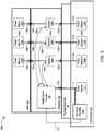
- FIG. 1 is a block diagram of an example integrated power sequencing circuit in a silicon interposer.
- FIG. 1 is an example apparatus 100 that includes a sequencer circuit controller 144 located in an ASIC 140 and that controls switch signals for a sequenced power up process.
- the apparatus 100 includes a circuit board 110, a package substrate 120, an interposer 130, and an ASIC 140.
- the circuit board 110 includes power source 112, which supplies power to a core power rail 111, and power sources 114a, 114b, 114n, etc., which supply power to power rails 113a, 113b, 113n, etc. (hereinafter generally referred to as power rails 113), respectively.
- power rails 113 are electrically connected to power connectors in the interposer 130 through the package substrate 120, as further described herein.
- the presented combination of power rails and power sources is for exemplary purposes only, and is not intended to be limiting in a one-to-one ratio.
- one power source may provide power to two or more power rails.
- power source 114a may provide power to both power rails 113a and 113b, thus, power source 114b would not be necessary.
- the interposer 130 electrically couples ASIC 140 to the circuit board 110 through the package substrate 120.
- the package substrate 120 includes a circuit board-facing side at a first end, and an interposer-facing side at a second end.
- the package substrate 120 provides the apparatus 100 with a mechanical base support and a form of an electrical interface that allows external components or circuits (e.g., the interposer 130 and ASIC 140) access to the device (e.g., circuit board 110) housed within on the circuit board-facing side of the package substrate 120.
- vertical through vias (or other conduction means) are formed in the package substrate 120 and are controlled by switches.
- the package substrate 120 may be composed of any known used material such as an epoxy-based laminate, resin-based laminate, a polymer material used as a tape substrate, or the like.
- a core power rail 111 is a vertical through via and shown in the vertical direction in the package substrate 120 and interposer 130, but there is a horizontal bifurcation of the core power rail 111 in the interposer 130 in a horizontal direction that provides power to the switch control circuitry 134.
- the package substrate 120 may include several layers with metal planes or traces that are interconnected to each other by through-hole plated vias.
- the package substrate 120 can include metal conductors that can accomplish this routing function.
- the package substrate 120 includes alternate means of providing an electrical connection such that the power rails 111 and 113 are electrically connected through the package substrate 120 from the circuit board 110 to the interposer 130.
- the interposer 130 includes switch control circuitry 134 and a plurality of switches 132a, 132b, 132n, (also referred to herein as switches 132).
- the switch control circuitry 134 includes control logic that generates switch signals 136a, 136b, 136n, etc. (also referred to herein as switch signals 136) to control the switches 132a, 132b, 132n, respectively, in order to control power for each respective power rail 133, as will be discussed in greater detail in connection with FIG. 2 .
- the interposer 130 further includes a plurality of power connectors 131, 133a, 133b, 133n, etc., on the surface of the substrate-facing side of the interposer 130, and a plurality of power connectors 137, 135a, 135b, 135n, etc., on the surface of the ASIC-facing side of the interposer 130.
- Each of the power connectors may include microbumps to electrically couple the respective power rails 113 to either the ASIC 140 or the circuit board 110 through the package substrate 120.
- power connector 131 is electrically coupled to the core power rail 111, and is connected to the package substrate 131 by a microbump.
- solder bumps may be used for the electrical connections described herein for the plurality of power connectors.
- microbumps may be used for one particular set of power connectors for the electrical connections, and solder bumps may be used for the electrical connections described herein for a different set of power connectors.
- the set of power connectors on the substrate-facing side of the interposer 130 e.g., power connectors 131, 133a-133n
- the set of power connectors on the ASIC-facing side of the interposer 130 may include microbumps to electrically connect the interposer 130 to the set of power connectors on the interposer-facing side of the ASIC 140 (e.g., power connectors 147, 146a-146n).
- the ASIC 140 includes an interposer-facing side at a first end, and an external-facing side at a second end.
- the ASIC 140 includes components such as a controller 144 and a plurality of power inputs 142a, 142b, 142n, etc. (also referred to herein as power inputs 142). Additionally, ASIC 140 includes a plurality of power connectors 147, 146a, 146b, 146n, etc., on the surface of the interposer-facing side of the ASIC 140 that are able to be electrically connected to the interposer 130.
- the controller 144 includes a sequencer circuit that generates and sends a control input signal 145 to the control input of the switch control circuitry 134 in the interposer 130.
- a plurality of different values are generated for the control input signal, where each value of the control input signal 145 causes the control logic of the switch control circuitry 134 to generate a corresponding set of switch signals 136 to control each of the switches 132.
- the plurality of different values for the control input signal 145 are generated by the controller 144 according to a predefined sequence to provide power to the ASIC 140 according to power up sequence.
- the switches 132 turn on and off the individual power rails 113 to the power inputs 142 of the ASIC 140.
- the timing of the control signals and the power gate switching delay are designed such that the sequencing can meet with the particular specification of the ASIC 140.
- a different ASIC 140 with different power up sequencing instructions for the power inputs 142 can be coupled to the switch control circuitry 134 of the interposer 130 and provide a different power up sequence event for the particular ASIC.
- FIG. 2 is an example circuit arrangement 200 of an active silicon interposer, such as interposer 130 of FIG. 1 .
- interposer 130 is receiving power on the substrate-facing side of the interposer 130 from a core rail power source for the core power rail 111, as well as receiving power from other input power sources VDD1, VDD2, VDDn, etc., for the sequencing power rails 113a, 113b, 113n, etc., respectively.
- the interposer 130 is operable to providing power output on the ASIC-facing side of the interposer 130 for core rail power for the core power rail 111, as well as providing output power VDD1', VDD2', VDDn', etc., to other components for the sequencing power rails 113a, 113b, 113n, etc., respectively.
- the switch control circuitry 134 includes control logic 204 and delay circuitry 206.
- the control logic 204 and delay circuitry 206 each include a power input to receive the core power from the core power rail 111.
- the controller 144 also receives power from the control core power rail 111, and thus is not required to be "switched on.”
- the control logic 204 includes a control input that receives a control input signal 202 (e.g., control input signal 145 from FIG. 1 ) that is received by the switch control circuitry 134 from a sequencer circuit (e.g., controller 144 of the ASIC 140, or an on-board controller on the circuit board 110 as further described herein with reference to FIG. 3 ).
- the controller 144 generates control signals so that that ASIC 140 may be powered up according to a controlled power sequence, e.g., rails may be powered in a specific pre-defined sequence that ensures the ASIC 140, once completely powered up, will operate according to specification and without power-induced errors.
- the control logic 204 provides an output signal 205 to an input of the delay circuitry 206.
- the delay circuitry then generates the switch signals 136a, 136b, 136n, etc., for each respective switch 132a, 132b, 132n, etc., according to a power sequencing process received in the control input signal 202.
- the switch signals 136 include a first state and a second state.
- the switch when the switch signal is in a first state, the switch is in a closed position to electrically connect the first terminal to the second terminal, and when the switch signal is in a second state the switch is in an open position to electrically isolate the first terminal from the second terminal.
- the control logic can be implemented by any appropriate control circuitry that provides switch signals for switches.
- each switch 132a, 132b, 132n includes a first terminal, a second terminal, and a third terminal.
- the third terminal of the each switch receives a control signal that places the first switch in either a closed state in which a conduction path is established between the first and second terminals, or an open state in which the conduction path is eliminated between the first and second terminals.
- the switches 132 or referred to as power gates, turn on and off individual power rails.
- switch 132a is used to switch the power on and off from the power rail 113a (e.g., VDD1) from the power connector 133a on the substrate-facing side of the interposer 130 to the power connector 135a on the ASIC-facing side of the interposer 130.
- switch 132a receives switch signal 136a at the third terminal of the switch 132a that places the switch 132a in a closed state in which a conduction path is established between the first and second terminals of switch 132a, and the output power VDD1' is now provided as an output from the power connector 135a to a connecting device, such as ASIC 140 in FIG. 1 .
- switch 132a receives switch signal 136a at the third terminal of the switch 132a that places the switch 132a in an open state in which the conduction path is eliminated between the first and second terminals of switch 132a, and the power VDD1 is now prohibited as an output from the power connector 135a to a connecting device, such as ASIC 140 in FIG. 1 .
- the interposer 130 includes one or more charge pumps used to elevate the driving voltage of the switch signals 136 and fully open the switches 132.
- charge pump 210 is connected to switch signal 136n.
- the charge pump 210 can boost the voltage for the switch signal 136n in order to provide a voltage that enables switch 132n is fully open to provide the expected power from the power rail 113n (VDDn) to a component that is electrically connected to the ASIC-facing side of the interposer 130, such as ASIC 140 in FIG. 1 .
- the charge pump 210 ensures that the input power received at power connector 133n (VDDn) is substantially similar to the output power at power connector 135n (VDDn').
- FIG. 3 is a block diagram of an example integrated power sequencing circuit in a silicon interposer.
- FIG. 3 is an example apparatus 300 includes a sequencer circuit that controls switch signals through a controller on a circuit board.
- the apparatus 300 has a topology similar to apparatus 100 shown in FIG. 1 , except that an on-board controller 316 on the circuit board 310 provides the control input signal 317 to the switch control circuitry 134, instead of the control input signal 145 from the controller 144 of the ASIC 140 as in FIG. 1 .
- the on-board controller 316 also referred to as a sequencer circuit, is electrically connected to core power rail 111 from the power source 112.
- the core power rail is typically the first rail from the circuit board 310, and is also the first rail to turn on in the power rail sequencing process, and powers the integrated chip manager inside the on-board controller 316, which then executes the chip firmware, communicates with the switch control circuitry 134, and manages the rest of the sequencing process, as described herein.
- Embodiments of the subject matter and the operations described in this specification can be implemented in digital electronic circuitry, or in computer software, firmware, or hardware, including the structures disclosed in this specification and their structural equivalents, or in combinations of one or more of them.
- Embodiments of the subject matter described in this specification can be implemented as one or more computer programs, i.e., one or more modules of computer program instructions, encoded on computer storage medium for execution by, or to control the operation of, data processing apparatus.
- An exemplary embodiment can be summarized as an apparatus that includes an interposer, first power connectors that are disposed on a first surface and that receive respective power inputs from one or more power sources, second power connectors that are disposed on the second surface and that receive a respective third power connecter of an integrated circuit when the integrated circuit is mounted on the second surface of the interposer, a plurality of switches formed within the interposer, control circuitry formed within the interposer, and a sequencer circuit coupled to the control input of the control circuitry and that generates a different values for a control input signal that causes the control logic of the control circuitry to generate a corresponding set of switch signals, and the plurality of different values for the control input signal are generated according to a predefined sequence to provide power to the integrated circuit according to power up sequence.
Landscapes
- Engineering & Computer Science (AREA)
- Theoretical Computer Science (AREA)
- Power Engineering (AREA)
- Physics & Mathematics (AREA)
- General Engineering & Computer Science (AREA)
- General Physics & Mathematics (AREA)
- Human Computer Interaction (AREA)
- Dc-Dc Converters (AREA)
- Semiconductor Integrated Circuits (AREA)
- Electronic Switches (AREA)
- Power Sources (AREA)
- Logic Circuits (AREA)
Abstract
Description
- Large computer, storage, or networking server systems used in datacenters usually consist of a fairly large number of power rails. When a circuit board is powered up, powered off, or going into different power states (such as fault or throttled), all of these rails need to be powered up/down in a specific order for the chips and active components on the board to be functional, or to behave (such as turn on/off, sleep) corresponding to the definition of the power state. This process is called power sequencing which is typically performed by a dedicated component on-board called a sequencer. Typical simpler boards will have one sequencer with pre-programmed firmware that contains the order and delay information which controls the sequencing of all power rails. When the number of power rails become large, more of such devices are needed and they take precious board space, add design complexity, and become hard to manage. In some cases, a "master-slave" configuration of multiple sequencers need to be maintained, further complicating the board level design.
- The circuits that are power sequenced include a silicon interposer below the silicon die and above the package substrate for an electrical interface routing between one socket or connection to another. The purpose of an interposer is to spread a connection to a wider pitch or to reroute a connection to a different connection.
- This specification describes technologies relating to systems and methods for integrating a power sequencing circuit into an electrical circuit silicon interposer.
- In general, one innovative aspect of the subject matter described in this specification can be embodied in an apparatus including an interposer having a first surface and a second surface that is opposite the first surface, first power connectors that are disposed on the first surface and that receive respective power inputs from one or more power sources, second power connectors that are disposed on the second surface and that receive a respective third power connecter of an integrated circuit when the integrated circuit is mounted on the second surface of the interposer, a plurality of switches formed within the interposer, control circuitry formed within the interposer, and a sequencer circuit coupled to the control input of the control circuitry and that generates the control input signal. Each switch has a first terminal connected to one of the first power connectors, a second terminal connected to one of the second power connectors, and a switch control input that receives a switch signal, wherein when the switch signal is in a first state the switch is in a closed position to electrically connect the first terminal to the second terminal, and when the switch signal is in a second state the switch is in an open position to electrically isolate the first terminal from the second terminal. The control circuity includes a control input that receives a control input signal a plurality of control outputs, each control output connected to a switch control input and control logic coupled to the control input and the plurality of control outputs, and based on a particular state of the control input signal applied to the control input, generates a corresponding set of switch signals on the control outputs to control the plurality of switches. The sequencer circuit generates a plurality of different values for the control input signal, where each value of the control input signal causes the control logic of the control circuitry to generate a corresponding set of switch signals, and the plurality of different values for the control input signal are generated according to a predefined sequence to provide power to the integrated circuit according to power up sequence.
- These and other embodiments can each optionally include one or more of the following features.
- In some aspects, the sequencer circuit is included in the integrated circuit, and the interposer includes a core rail connection that is not controlled by a switch and that provides power to a core rail of the integrated circuit, and wherein the sequencer circuit is powered by the core rail.
- In some aspects, the sequencer circuit is included in a circuit board upon which the interposer is mounted by the first surface, and the sequencer circuit is connected to a power rail in the circuit board.
- In some aspects, the apparatus further includes a circuit board, and a package layer having a first surface and a second surface that is opposite the first surface, wherein the first surface of the package layer is mounted to the circuit board, and the second surface of the package layer is mounted to the first surface of the interposer.
- In some aspects, the apparatus further includes a charge pump circuit that boosts an input voltage of a switch signal for a particular switch and provides the boosted input voltage of the switch signal to a switch control input of the particular switch.
- In some aspects, the switches are MOSFETs.
- Particular embodiments of the subject matter described in this specification can be implemented so as to realize one or more of the following advantages. The benefit of the active interposer circuit arrangement described herein is that each integrated circuit is self-contained in fulfilling its power sequencing requirement. The sequencing requirement can be directly written or changed in the integrated circuit firmware or on-board controller firmware. Additionally, the active interposer circuit arrangement removes multiple power sequencers on the board, creating extra space for additional features and power savings.
- The details of one or more embodiments of the subject matter described in this specification are set forth in the accompanying drawings and the description below. Other features, aspects, and advantages of the subject matter will become apparent from the description, the drawings, and the claims.
-
-
FIG. 1 is a block diagram of an example integrated power sequencing circuit in a silicon interposer. -
FIG. 2 is an example circuit arrangement of an active silicon interposer. -
FIG. 3 is a block diagram of another example integrated power sequencing circuit in a silicon interposer. - Like reference numbers and designations in the various drawings indicate like elements.
- The subject matter of this written description relates to systems and methods for integrating a power sequencing circuit into an circuit device's silicon interposer, such as an application-specific integrated circuits (ASIC's) silicon interposer. This disclosure describes an apparatus that implements power sequencing with logic and delay circuitry in the interposer, and controlled by a controller either in the ASIC or an on-board controller in the circuit board. In the examples below, an ASIC is described, but it is to be understood that other integrated circuits can also benefit from the power sequencing in the silicon interposer.
- Modern high-performance ASIC's widely use a silicon interposer below the silicon die and above the package substrate to connect high-speed signals from computer die to memory die or transceiver chips. Silicon interposers are typically made with older technology nodes and are passive. This disclosure proposes an apparatus that implements logic and delay circuitry in the interposer, which is active and functions as in-package power sequencer for the power rails for the ASIC die(s) that are assembled on the interposer.
- In one implementation an apparatus includes an interposer, first power connectors that receive respective power inputs from one or more power sources, second power connectors that receive a respective third power connecter of an integrated circuit when the integrated circuit is mounted on the interposer, a plurality of switches formed within the interposer, and control circuitry formed within the interposer. The control circuity includes a control input that receives a control input signal, a plurality of control outputs, each control output connected to a switch control input, and control logic that generates a corresponding set of switch signals on the control outputs to control the plurality of switches.
- In some implementations, the sequencing logic is stored in the firmware on the ASIC's integrated controller. The in-package sequencing circuits (e.g., switches) have control signals connected to the ASIC itself. Alternatively, or additionally, in some implementations, the sequencing logic is stored in firmware on an embedded on-board controller on the circuit board, and the sequencing circuits have control signals connected to the on-board controller.
- These features and additional features are described in more detail below.
-
FIG. 1 is a block diagram of an example integrated power sequencing circuit in a silicon interposer. In particular,FIG. 1 is anexample apparatus 100 that includes asequencer circuit controller 144 located in anASIC 140 and that controls switch signals for a sequenced power up process. As shown, theapparatus 100 includes acircuit board 110, apackage substrate 120, aninterposer 130, and an ASIC 140. - The
circuit board 110 includespower source 112, which supplies power to acore power rail 111, andpower sources power rails power rails 111 and 113 are electrically connected to power connectors in theinterposer 130 through thepackage substrate 120, as further described herein. As shown inFIG. 1 , the presented combination of power rails and power sources is for exemplary purposes only, and is not intended to be limiting in a one-to-one ratio. In some implementations, one power source may provide power to two or more power rails. For example,power source 114a, may provide power to bothpower rails power source 114b would not be necessary. - The interposer 130 electrically couples ASIC 140 to the
circuit board 110 through thepackage substrate 120. Thepackage substrate 120 includes a circuit board-facing side at a first end, and an interposer-facing side at a second end. Thepackage substrate 120 provides theapparatus 100 with a mechanical base support and a form of an electrical interface that allows external components or circuits (e.g., theinterposer 130 and ASIC 140) access to the device (e.g., circuit board 110) housed within on the circuit board-facing side of thepackage substrate 120. In order to electrically connect ASIC 140 and interposer 130 to thecircuit board 110, vertical through vias (or other conduction means) are formed in thepackage substrate 120 and are controlled by switches. Thepackage substrate 120 may be composed of any known used material such as an epoxy-based laminate, resin-based laminate, a polymer material used as a tape substrate, or the like. For example, as shown inFIG. 1 , acore power rail 111 is a vertical through via and shown in the vertical direction in thepackage substrate 120 and interposer 130, but there is a horizontal bifurcation of thecore power rail 111 in theinterposer 130 in a horizontal direction that provides power to theswitch control circuitry 134. - To electrically couple the
interposer 130 and ASIC 140 to thecircuit board 110, thepackage substrate 120 may include several layers with metal planes or traces that are interconnected to each other by through-hole plated vias. Thus, thepackage substrate 120 can include metal conductors that can accomplish this routing function. Additionally, or alternatively, thepackage substrate 120 includes alternate means of providing an electrical connection such that thepower rails 111 and 113 are electrically connected through thepackage substrate 120 from thecircuit board 110 to theinterposer 130. - As shown in
FIG. 1 , theinterposer 130 includesswitch control circuitry 134 and a plurality ofswitches switch control circuitry 134 includes control logic that generatesswitch signals switches FIG. 2 . - The
interposer 130 further includes a plurality ofpower connectors interposer 130, and a plurality ofpower connectors interposer 130. Each of the power connectors may include microbumps to electrically couple the respective power rails 113 to either theASIC 140 or thecircuit board 110 through thepackage substrate 120. For example,power connector 131 is electrically coupled to thecore power rail 111, and is connected to thepackage substrate 131 by a microbump. Alternatively, solder bumps may be used for the electrical connections described herein for the plurality of power connectors. Alternatively, microbumps may be used for one particular set of power connectors for the electrical connections, and solder bumps may be used for the electrical connections described herein for a different set of power connectors. For example, the set of power connectors on the substrate-facing side of the interposer 130 (e.g.,power connectors interposer 130 to thepackage substrate 120. Additionally, the set of power connectors on the ASIC-facing side of the interposer 130 (e.g.,power connectors interposer 130 to the set of power connectors on the interposer-facing side of the ASIC 140 (e.g.,power connectors - The
ASIC 140 includes an interposer-facing side at a first end, and an external-facing side at a second end. TheASIC 140 includes components such as acontroller 144 and a plurality ofpower inputs ASIC 140 includes a plurality ofpower connectors ASIC 140 that are able to be electrically connected to theinterposer 130. - In the example implementation as shown in
FIG. 1 , thecontroller 144 includes a sequencer circuit that generates and sends acontrol input signal 145 to the control input of theswitch control circuitry 134 in theinterposer 130. A plurality of different values are generated for the control input signal, where each value of thecontrol input signal 145 causes the control logic of theswitch control circuitry 134 to generate a corresponding set of switch signals 136 to control each of the switches 132. For example, the plurality of different values for thecontrol input signal 145 are generated by thecontroller 144 according to a predefined sequence to provide power to theASIC 140 according to power up sequence. The switches 132 turn on and off the individual power rails 113 to the power inputs 142 of theASIC 140. The timing of the control signals and the power gate switching delay are designed such that the sequencing can meet with the particular specification of theASIC 140. Thus, adifferent ASIC 140 with different power up sequencing instructions for the power inputs 142 can be coupled to theswitch control circuitry 134 of theinterposer 130 and provide a different power up sequence event for the particular ASIC. -
FIG. 2 is anexample circuit arrangement 200 of an active silicon interposer, such asinterposer 130 ofFIG. 1 . In thisexample circuit arrangement 200,interposer 130 is receiving power on the substrate-facing side of theinterposer 130 from a core rail power source for thecore power rail 111, as well as receiving power from other input power sources VDD1, VDD2, VDDn, etc., for thesequencing power rails interposer 130 is operable to providing power output on the ASIC-facing side of theinterposer 130 for core rail power for thecore power rail 111, as well as providing output power VDD1', VDD2', VDDn', etc., to other components for thesequencing power rails - The
switch control circuitry 134 includescontrol logic 204 anddelay circuitry 206. Thecontrol logic 204 anddelay circuitry 206 each include a power input to receive the core power from thecore power rail 111. Thecontroller 144 also receives power from the controlcore power rail 111, and thus is not required to be "switched on." Thecontrol logic 204 includes a control input that receives a control input signal 202 (e.g., control input signal 145 fromFIG. 1 ) that is received by theswitch control circuitry 134 from a sequencer circuit (e.g.,controller 144 of theASIC 140, or an on-board controller on thecircuit board 110 as further described herein with reference toFIG. 3 ). Thecontroller 144 generates control signals so that thatASIC 140 may be powered up according to a controlled power sequence, e.g., rails may be powered in a specific pre-defined sequence that ensures theASIC 140, once completely powered up, will operate according to specification and without power-induced errors. Thecontrol logic 204 provides anoutput signal 205 to an input of thedelay circuitry 206. The delay circuitry then generates the switch signals 136a, 136b, 136n, etc., for eachrespective switch control input signal 202. The switch signals 136 include a first state and a second state. For example, when the switch signal is in a first state, the switch is in a closed position to electrically connect the first terminal to the second terminal, and when the switch signal is in a second state the switch is in an open position to electrically isolate the first terminal from the second terminal. The control logic can be implemented by any appropriate control circuitry that provides switch signals for switches. - The switches 132 in the example embodiment are MOSFETS, however, different types of switches may be used. As shown in
FIG. 2 , eachswitch switch 132a is used to switch the power on and off from thepower rail 113a (e.g., VDD1) from thepower connector 133a on the substrate-facing side of theinterposer 130 to thepower connector 135a on the ASIC-facing side of theinterposer 130. In operation, during an on state,switch 132a receivesswitch signal 136a at the third terminal of theswitch 132a that places theswitch 132a in a closed state in which a conduction path is established between the first and second terminals ofswitch 132a, and the output power VDD1' is now provided as an output from thepower connector 135a to a connecting device, such asASIC 140 inFIG. 1 . During an off state,switch 132a receivesswitch signal 136a at the third terminal of theswitch 132a that places theswitch 132a in an open state in which the conduction path is eliminated between the first and second terminals ofswitch 132a, and the power VDD1 is now prohibited as an output from thepower connector 135a to a connecting device, such asASIC 140 inFIG. 1 . - In some implementations, the
interposer 130 includes one or more charge pumps used to elevate the driving voltage of the switch signals 136 and fully open the switches 132. For example, as shown inFIG. 2 ,charge pump 210 is connected to switchsignal 136n. In operation, thecharge pump 210 can boost the voltage for theswitch signal 136n in order to provide a voltage that enablesswitch 132n is fully open to provide the expected power from thepower rail 113n (VDDn) to a component that is electrically connected to the ASIC-facing side of theinterposer 130, such asASIC 140 inFIG. 1 . Thus, thecharge pump 210 ensures that the input power received atpower connector 133n (VDDn) is substantially similar to the output power atpower connector 135n (VDDn'). -
FIG. 3 is a block diagram of an example integrated power sequencing circuit in a silicon interposer. In particular,FIG. 3 is anexample apparatus 300 includes a sequencer circuit that controls switch signals through a controller on a circuit board. Theapparatus 300 has a topology similar toapparatus 100 shown inFIG. 1 , except that an on-board controller 316 on thecircuit board 310 provides thecontrol input signal 317 to theswitch control circuitry 134, instead of the control input signal 145 from thecontroller 144 of theASIC 140 as inFIG. 1 . - As shown in
FIG. 3 , the on-board controller 316, also referred to as a sequencer circuit, is electrically connected tocore power rail 111 from thepower source 112. The core power rail is typically the first rail from thecircuit board 310, and is also the first rail to turn on in the power rail sequencing process, and powers the integrated chip manager inside the on-board controller 316, which then executes the chip firmware, communicates with theswitch control circuitry 134, and manages the rest of the sequencing process, as described herein. - Embodiments of the subject matter and the operations described in this specification can be implemented in digital electronic circuitry, or in computer software, firmware, or hardware, including the structures disclosed in this specification and their structural equivalents, or in combinations of one or more of them. Embodiments of the subject matter described in this specification can be implemented as one or more computer programs, i.e., one or more modules of computer program instructions, encoded on computer storage medium for execution by, or to control the operation of, data processing apparatus.
- While this specification contains many specific implementation details, these should not be construed as limitations on the scope of any features or of what may be claimed, but rather as descriptions of features specific to particular embodiments. Certain features that are described in this specification in the context of separate embodiments can also be implemented in combination in a single embodiment. Conversely, various features that are described in the context of a single embodiment can also be implemented in multiple embodiments separately or in any suitable subcombination. Moreover, although features may be described above as acting in certain combinations and even initially claimed as such, one or more features from a claimed combination can in some cases be excised from the combination, and the claimed combination may be directed to a subcombination or variation of a subcombination.
- Thus, particular embodiments of the subject matter have been described. Other embodiments are within the scope of the following claims. In some cases, the actions recited in the claims can be performed in a different order and still achieve desirable results. In addition, the processes depicted in the accompanying figures do not necessarily require the particular order shown, or sequential order, to achieve desirable results. In certain implementations, multitasking and parallel processing may be advantageous.
- An exemplary embodiment can be summarized as an apparatus that includes an interposer, first power connectors that are disposed on a first surface and that receive respective power inputs from one or more power sources, second power connectors that are disposed on the second surface and that receive a respective third power connecter of an integrated circuit when the integrated circuit is mounted on the second surface of the interposer, a plurality of switches formed within the interposer, control circuitry formed within the interposer, and a sequencer circuit coupled to the control input of the control circuitry and that generates a different values for a control input signal that causes the control logic of the control circuitry to generate a corresponding set of switch signals, and the plurality of different values for the control input signal are generated according to a predefined sequence to provide power to the integrated circuit according to power up sequence.
Claims (6)
- An apparatus, comprising:an interposer having a first surface and a second surface that is opposite the first surface;first power connectors that are disposed on the first surface and that receive respective power inputs from one or more power sources;second power connectors that are disposed on the second surface and that receive a respective third power connecter of an integrated circuit when the integrated circuit is mounted on the second surface of the interposer;a plurality of switches formed within the interposer, wherein each switch has a first terminal connected to one of the first power connectors, a second terminal connected to one of the second power connectors, and a switch control input that receives a switch signal, wherein when the switch signal is in a first state the switch is in a closed position to electrically connect the first terminal to the second terminal, and when the switch signal is in a second state the switch is in an open position to electrically isolate the first terminal from the second terminal;control circuitry formed within the interposer, the control circuity including:a control input that receives a control input signal;a plurality of control outputs, each control output connected to a switch control input; andcontrol logic coupled to the control input and the plurality of control outputs, and based on a particular state of the control input signal applied to the control input, generates a corresponding set of switch signals on the control outputs to control the plurality of switches; anda sequencer circuit coupled to the control input of the control circuitry and that generates the control input signal, wherein the sequencer circuit generates a plurality of different values for the control input signal, where each value of the control input signal causes the control logic of the control circuitry to generate a corresponding set of switch signals, and the plurality of different values for the control input signal are generated according to a predefined sequence to provide power to the integrated circuit according to power up sequence.
- The apparatus of claim 1, wherein:the sequencer circuit is included in the integrated circuit; andthe interposer includes a core rail connection that is not controlled by a switch and that provides power to a core rail of the integrated circuit, and wherein the sequencer circuit is powered by the core rail.
- The apparatus of claim 1, wherein
the sequencer circuit is included in a circuit board upon which the interposer is mounted by the first surface; and
the sequencer circuit is connected to a power rail in the circuit board. - The apparatus of one of claims 1 to 3, further comprising:a circuit board; anda package layer having a first surface and a second surface that is opposite the first surface, wherein the first surface of the package layer is mounted to the circuit board, and the second surface of the package layer is mounted to the first surface of the interposer.
- The apparatus of one of claims 1 to 4, further comprising a charge pump circuit that boosts an input voltage of a switch signal for a particular switch and provides the boosted input voltage of the switch signal to a switch control input of the particular switch.
- The apparatus of one of claims 1 to 5, wherein the switches are MOSFETs.
Priority Applications (1)
| Application Number | Priority Date | Filing Date | Title |
|---|---|---|---|
| EP24182119.8A EP4407407A3 (en) | 2019-07-31 | 2020-07-30 | Power sequencing in an active silicon interposer |
Applications Claiming Priority (1)
| Application Number | Priority Date | Filing Date | Title |
|---|---|---|---|
| US16/527,569 US10742211B1 (en) | 2019-07-31 | 2019-07-31 | Power sequencing in an active silicon interposer |
Related Child Applications (2)
| Application Number | Title | Priority Date | Filing Date |
|---|---|---|---|
| EP24182119.8A Division EP4407407A3 (en) | 2019-07-31 | 2020-07-30 | Power sequencing in an active silicon interposer |
| EP24182119.8A Division-Into EP4407407A3 (en) | 2019-07-31 | 2020-07-30 | Power sequencing in an active silicon interposer |
Publications (2)
| Publication Number | Publication Date |
|---|---|
| EP3771962A1 true EP3771962A1 (en) | 2021-02-03 |
| EP3771962B1 EP3771962B1 (en) | 2024-09-04 |
Family
ID=71894686
Family Applications (2)
| Application Number | Title | Priority Date | Filing Date |
|---|---|---|---|
| EP24182119.8A Pending EP4407407A3 (en) | 2019-07-31 | 2020-07-30 | Power sequencing in an active silicon interposer |
| EP20188629.8A Active EP3771962B1 (en) | 2019-07-31 | 2020-07-30 | Power sequencing in an active silicon interposer |
Family Applications Before (1)
| Application Number | Title | Priority Date | Filing Date |
|---|---|---|---|
| EP24182119.8A Pending EP4407407A3 (en) | 2019-07-31 | 2020-07-30 | Power sequencing in an active silicon interposer |
Country Status (6)
| Country | Link |
|---|---|
| US (2) | US10742211B1 (en) |
| EP (2) | EP4407407A3 (en) |
| CN (2) | CN112305985B (en) |
| DK (1) | DK3771962T3 (en) |
| FI (1) | FI3771962T3 (en) |
| TW (2) | TWI749666B (en) |
Cited By (1)
| Publication number | Priority date | Publication date | Assignee | Title |
|---|---|---|---|---|
| EP4296805A4 (en) * | 2021-03-24 | 2025-04-09 | Fanuc Corporation | ELECTRONIC DEVICE |
Families Citing this family (3)
| Publication number | Priority date | Publication date | Assignee | Title |
|---|---|---|---|---|
| US20230223402A1 (en) * | 2022-01-12 | 2023-07-13 | Kneron Inc. | Three-dimensional Integrated Circuit |
| US12389527B2 (en) | 2023-08-07 | 2025-08-12 | Ciena Corporation | ASIC busbar with remote power phases for telecommunications and networking shelf and circuit card assemblies |
| EP4672883A3 (en) * | 2023-08-07 | 2026-03-25 | Ciena Corporation | Asic busbar with remote power phases for telecommunications and networking shelf and circuit card assemblies |
Citations (3)
| Publication number | Priority date | Publication date | Assignee | Title |
|---|---|---|---|---|
| US20090115256A1 (en) * | 2007-11-05 | 2009-05-07 | Arm Limited | Dynamically changing control of sequenced power gating |
| US20150081123A1 (en) * | 2013-09-13 | 2015-03-19 | International Business Machines Corporation | Predictively turning off a charge pump supplying voltage for overdriving gates of the power switch header in a microprocessor with power gating |
| US9935052B1 (en) * | 2014-11-26 | 2018-04-03 | Altera Corporation | Power line layout in integrated circuits |
Family Cites Families (22)
| Publication number | Priority date | Publication date | Assignee | Title |
|---|---|---|---|---|
| EP0552288A1 (en) * | 1990-10-03 | 1993-07-28 | Thinking Machines Corporation | Parallel computer system |
| CN2718635Y (en) * | 2004-03-03 | 2005-08-17 | 中兴通讯股份有限公司 | Multi-power source charging sequential control circuit |
| CN100492228C (en) * | 2005-05-30 | 2009-05-27 | 杭州华三通信技术有限公司 | Device and method for controlling multi-voltage power-on sequence |
| US7574540B2 (en) * | 2006-01-03 | 2009-08-11 | Emc Corporation | Managing management controller communications |
| KR100806127B1 (en) * | 2006-09-06 | 2008-02-22 | 삼성전자주식회사 | Power gating circuits and power gating methods reduce peak current |
| US7898072B2 (en) * | 2008-07-11 | 2011-03-01 | Stats Chippac Ltd. | Package stacking system with mold contamination prevention |
| US8907462B2 (en) * | 2009-02-05 | 2014-12-09 | Hewlett-Packard Development Company, L. P. | Integrated circuit package |
| US8680710B2 (en) * | 2010-12-17 | 2014-03-25 | Texas Instruments Incorporated | Analog power sequencer and method |
| US9153508B2 (en) * | 2011-08-17 | 2015-10-06 | Rambus Inc. | Multi-chip package and interposer with signal line compression |
| US8873320B2 (en) * | 2011-08-17 | 2014-10-28 | Taiwan Semiconductor Manufacturing Co., Ltd. | DRAM repair architecture for wide I/O DRAM based 2.5D/3D system chips |
| US8751836B1 (en) * | 2011-12-28 | 2014-06-10 | Datadirect Networks, Inc. | Data storage system and method for monitoring and controlling the power budget in a drive enclosure housing data storage devices |
| US9633872B2 (en) * | 2013-01-29 | 2017-04-25 | Altera Corporation | Integrated circuit package with active interposer |
| US9106229B1 (en) * | 2013-03-14 | 2015-08-11 | Altera Corporation | Programmable interposer circuitry |
| US9059696B1 (en) * | 2013-08-01 | 2015-06-16 | Altera Corporation | Interposer with programmable power gating granularity |
| US9298253B2 (en) * | 2013-09-13 | 2016-03-29 | Globalfoundries Inc. | Accelerating the microprocessor core wakeup by predictively executing a subset of the power-up sequence |
| JP6495698B2 (en) * | 2014-03-20 | 2019-04-03 | 株式会社半導体エネルギー研究所 | Semiconductor device, electronic component, and electronic device |
| JP6417781B2 (en) * | 2014-08-13 | 2018-11-07 | 株式会社ソシオネクスト | Semiconductor device |
| TW201643772A (en) | 2015-06-08 | 2016-12-16 | 指紋卡公司 | Fingerprint sensing device with interposer structure |
| CN105786144B (en) * | 2016-02-02 | 2019-03-15 | 广东技术师范学院 | A processor multi-power management control device, system and method |
| US10665579B2 (en) * | 2016-02-16 | 2020-05-26 | Xilinx, Inc. | Chip package assembly with power management integrated circuit and integrated circuit die |
| US9917517B1 (en) * | 2016-10-26 | 2018-03-13 | Google Inc. | Switched tank converter |
| US11036660B2 (en) * | 2019-03-28 | 2021-06-15 | Intel Corporation | Network-on-chip for inter-die and intra-die communication in modularized integrated circuit devices |
-
2019
- 2019-07-31 US US16/527,569 patent/US10742211B1/en active Active
-
2020
- 2020-07-06 US US16/921,571 patent/US11552634B2/en active Active
- 2020-07-27 TW TW109125275A patent/TWI749666B/en active
- 2020-07-27 TW TW110141976A patent/TWI800087B/en active
- 2020-07-30 CN CN202010748713.1A patent/CN112305985B/en active Active
- 2020-07-30 EP EP24182119.8A patent/EP4407407A3/en active Pending
- 2020-07-30 EP EP20188629.8A patent/EP3771962B1/en active Active
- 2020-07-30 DK DK20188629.8T patent/DK3771962T3/en active
- 2020-07-30 CN CN202411003268.0A patent/CN118963518A/en active Pending
- 2020-07-30 FI FIEP20188629.8T patent/FI3771962T3/en active
Patent Citations (3)
| Publication number | Priority date | Publication date | Assignee | Title |
|---|---|---|---|---|
| US20090115256A1 (en) * | 2007-11-05 | 2009-05-07 | Arm Limited | Dynamically changing control of sequenced power gating |
| US20150081123A1 (en) * | 2013-09-13 | 2015-03-19 | International Business Machines Corporation | Predictively turning off a charge pump supplying voltage for overdriving gates of the power switch header in a microprocessor with power gating |
| US9935052B1 (en) * | 2014-11-26 | 2018-04-03 | Altera Corporation | Power line layout in integrated circuits |
Cited By (2)
| Publication number | Priority date | Publication date | Assignee | Title |
|---|---|---|---|---|
| EP4296805A4 (en) * | 2021-03-24 | 2025-04-09 | Fanuc Corporation | ELECTRONIC DEVICE |
| US12471235B2 (en) | 2021-03-24 | 2025-11-11 | Fanuc Corporation | Electronic apparatus |
Also Published As
| Publication number | Publication date |
|---|---|
| CN118963518A (en) | 2024-11-15 |
| DK3771962T3 (en) | 2024-12-02 |
| CN112305985B (en) | 2024-08-23 |
| EP4407407A2 (en) | 2024-07-31 |
| EP3771962B1 (en) | 2024-09-04 |
| US10742211B1 (en) | 2020-08-11 |
| CN112305985A (en) | 2021-02-02 |
| EP4407407A3 (en) | 2024-10-30 |
| TW202226758A (en) | 2022-07-01 |
| US11552634B2 (en) | 2023-01-10 |
| US20210036702A1 (en) | 2021-02-04 |
| TWI800087B (en) | 2023-04-21 |
| TW202123611A (en) | 2021-06-16 |
| TWI749666B (en) | 2021-12-11 |
| FI3771962T3 (en) | 2024-12-07 |
Similar Documents
| Publication | Publication Date | Title |
|---|---|---|
| EP3771962B1 (en) | Power sequencing in an active silicon interposer | |
| CN102396030B (en) | Method and system for reducing trace length and capacitance in the context of large memory footprints | |
| US9276335B2 (en) | Double-sided circuit board with opposing modular card connector assemblies | |
| US12366882B2 (en) | Field programmable platform array | |
| US6661690B2 (en) | High capacity memory module with built-in performance enhancing features | |
| US11564317B2 (en) | Integrated power delivery board for delivering power to an ASIC with bypass of signal vias in a printed circuit board | |
| US20150359099A1 (en) | Low area over-head connectivity solutions to sip module | |
| JPH0477469B2 (en) | ||
| TWI524471B (en) | Microelectronic components with master/slave configurable settings | |
| CN110717569A (en) | Memory card, memory card slot and electronic system | |
| US6496380B1 (en) | High capacity memory module with high electrical design margins | |
| HK40042545A (en) | Power sequencing in an active silicon interposer | |
| HK40119300A (en) | Power sequencing in an active silicon interposer | |
| HK40042545B (en) | Power sequencing in an active silicon interposer | |
| US8837163B2 (en) | Integrated flex tail circuit packaging | |
| US5598035A (en) | Integrated circuit package with external storage capacitor for improved signal quality for sensitive integrated circuit elements | |
| JPH0685408A (en) | Multilayer printed circuit board device | |
| JPH03121501A (en) | Controller | |
| JP2007128959A (en) | Semiconductor memory card and circuit board | |
| TW202107777A (en) | Storage device having gold finger connection interface and electric connector | |
| CN115810606A (en) | Electronic equipment, circuit boards and semiconductor devices | |
| JP2009010410A (en) | Semiconductor device | |
| JPH0668942A (en) | Card edge connector | |
| JPH10283076A (en) | Mounting state detection circuit | |
| JP2006245613A (en) | Semiconductor device |
Legal Events
| Date | Code | Title | Description |
|---|---|---|---|
| PUAI | Public reference made under article 153(3) epc to a published international application that has entered the european phase |
Free format text: ORIGINAL CODE: 0009012 |
|
| STAA | Information on the status of an ep patent application or granted ep patent |
Free format text: STATUS: THE APPLICATION HAS BEEN PUBLISHED |
|
| AK | Designated contracting states |
Kind code of ref document: A1 Designated state(s): AL AT BE BG CH CY CZ DE DK EE ES FI FR GB GR HR HU IE IS IT LI LT LU LV MC MK MT NL NO PL PT RO RS SE SI SK SM TR |
|
| AX | Request for extension of the european patent |
Extension state: BA ME |
|
| STAA | Information on the status of an ep patent application or granted ep patent |
Free format text: STATUS: REQUEST FOR EXAMINATION WAS MADE |
|
| 17P | Request for examination filed |
Effective date: 20210713 |
|
| RBV | Designated contracting states (corrected) |
Designated state(s): AL AT BE BG CH CY CZ DE DK EE ES FI FR GB GR HR HU IE IS IT LI LT LU LV MC MK MT NL NO PL PT RO RS SE SI SK SM TR |
|
| STAA | Information on the status of an ep patent application or granted ep patent |
Free format text: STATUS: EXAMINATION IS IN PROGRESS |
|
| 17Q | First examination report despatched |
Effective date: 20220506 |
|
| GRAP | Despatch of communication of intention to grant a patent |
Free format text: ORIGINAL CODE: EPIDOSNIGR1 |
|
| STAA | Information on the status of an ep patent application or granted ep patent |
Free format text: STATUS: GRANT OF PATENT IS INTENDED |
|
| INTG | Intention to grant announced |
Effective date: 20240229 |
|
| RIN1 | Information on inventor provided before grant (corrected) |
Inventor name: CHUNG, CHEE YEE Inventor name: SIZIKOV, GREGORY Inventor name: JIANG, SHUAI Inventor name: POPOVICH, MIKHAIL Inventor name: GAN, HOULE |
|
| GRAS | Grant fee paid |
Free format text: ORIGINAL CODE: EPIDOSNIGR3 |
|
| GRAA | (expected) grant |
Free format text: ORIGINAL CODE: 0009210 |
|
| STAA | Information on the status of an ep patent application or granted ep patent |
Free format text: STATUS: THE PATENT HAS BEEN GRANTED |
|
| P01 | Opt-out of the competence of the unified patent court (upc) registered |
Free format text: CASE NUMBER: APP_43381/2024 Effective date: 20240724 |
|
| AK | Designated contracting states |
Kind code of ref document: B1 Designated state(s): AL AT BE BG CH CY CZ DE DK EE ES FI FR GB GR HR HU IE IS IT LI LT LU LV MC MK MT NL NO PL PT RO RS SE SI SK SM TR |
|
| REG | Reference to a national code |
Ref country code: GB Ref legal event code: FG4D |
|
| REG | Reference to a national code |
Ref country code: CH Ref legal event code: EP |
|
| REG | Reference to a national code |
Ref country code: IE Ref legal event code: FG4D |
|
| REG | Reference to a national code |
Ref country code: DE Ref legal event code: R096 Ref document number: 602020036965 Country of ref document: DE |
|
| REG | Reference to a national code |
Ref country code: DK Ref legal event code: T3 Effective date: 20241126 |
|
| REG | Reference to a national code |
Ref country code: FI Ref legal event code: FGE |
|
| REG | Reference to a national code |
Ref country code: NL Ref legal event code: FP |
|
| REG | Reference to a national code |
Ref country code: LT Ref legal event code: MG9D |
|
| REG | Reference to a national code |
Ref country code: SE Ref legal event code: TRGR |
|
| PG25 | Lapsed in a contracting state [announced via postgrant information from national office to epo] |
Ref country code: NO Free format text: LAPSE BECAUSE OF FAILURE TO SUBMIT A TRANSLATION OF THE DESCRIPTION OR TO PAY THE FEE WITHIN THE PRESCRIBED TIME-LIMIT Effective date: 20241204 |
|
| PG25 | Lapsed in a contracting state [announced via postgrant information from national office to epo] |
Ref country code: GR Free format text: LAPSE BECAUSE OF FAILURE TO SUBMIT A TRANSLATION OF THE DESCRIPTION OR TO PAY THE FEE WITHIN THE PRESCRIBED TIME-LIMIT Effective date: 20241205 Ref country code: PL Free format text: LAPSE BECAUSE OF FAILURE TO SUBMIT A TRANSLATION OF THE DESCRIPTION OR TO PAY THE FEE WITHIN THE PRESCRIBED TIME-LIMIT Effective date: 20240904 |
|
| PG25 | Lapsed in a contracting state [announced via postgrant information from national office to epo] |
Ref country code: BG Free format text: LAPSE BECAUSE OF FAILURE TO SUBMIT A TRANSLATION OF THE DESCRIPTION OR TO PAY THE FEE WITHIN THE PRESCRIBED TIME-LIMIT Effective date: 20240904 |
|
| PG25 | Lapsed in a contracting state [announced via postgrant information from national office to epo] |
Ref country code: LV Free format text: LAPSE BECAUSE OF FAILURE TO SUBMIT A TRANSLATION OF THE DESCRIPTION OR TO PAY THE FEE WITHIN THE PRESCRIBED TIME-LIMIT Effective date: 20240904 |
|
| PG25 | Lapsed in a contracting state [announced via postgrant information from national office to epo] |
Ref country code: HR Free format text: LAPSE BECAUSE OF FAILURE TO SUBMIT A TRANSLATION OF THE DESCRIPTION OR TO PAY THE FEE WITHIN THE PRESCRIBED TIME-LIMIT Effective date: 20240904 |
|
| PG25 | Lapsed in a contracting state [announced via postgrant information from national office to epo] |
Ref country code: ES Free format text: LAPSE BECAUSE OF FAILURE TO SUBMIT A TRANSLATION OF THE DESCRIPTION OR TO PAY THE FEE WITHIN THE PRESCRIBED TIME-LIMIT Effective date: 20240904 |
|
| PG25 | Lapsed in a contracting state [announced via postgrant information from national office to epo] |
Ref country code: PL Free format text: LAPSE BECAUSE OF FAILURE TO SUBMIT A TRANSLATION OF THE DESCRIPTION OR TO PAY THE FEE WITHIN THE PRESCRIBED TIME-LIMIT Effective date: 20240904 Ref country code: NO Free format text: LAPSE BECAUSE OF FAILURE TO SUBMIT A TRANSLATION OF THE DESCRIPTION OR TO PAY THE FEE WITHIN THE PRESCRIBED TIME-LIMIT Effective date: 20241204 Ref country code: LV Free format text: LAPSE BECAUSE OF FAILURE TO SUBMIT A TRANSLATION OF THE DESCRIPTION OR TO PAY THE FEE WITHIN THE PRESCRIBED TIME-LIMIT Effective date: 20240904 Ref country code: HR Free format text: LAPSE BECAUSE OF FAILURE TO SUBMIT A TRANSLATION OF THE DESCRIPTION OR TO PAY THE FEE WITHIN THE PRESCRIBED TIME-LIMIT Effective date: 20240904 Ref country code: GR Free format text: LAPSE BECAUSE OF FAILURE TO SUBMIT A TRANSLATION OF THE DESCRIPTION OR TO PAY THE FEE WITHIN THE PRESCRIBED TIME-LIMIT Effective date: 20241205 Ref country code: ES Free format text: LAPSE BECAUSE OF FAILURE TO SUBMIT A TRANSLATION OF THE DESCRIPTION OR TO PAY THE FEE WITHIN THE PRESCRIBED TIME-LIMIT Effective date: 20240904 Ref country code: BG Free format text: LAPSE BECAUSE OF FAILURE TO SUBMIT A TRANSLATION OF THE DESCRIPTION OR TO PAY THE FEE WITHIN THE PRESCRIBED TIME-LIMIT Effective date: 20240904 |
|
| REG | Reference to a national code |
Ref country code: AT Ref legal event code: MK05 Ref document number: 1721047 Country of ref document: AT Kind code of ref document: T Effective date: 20240904 |
|
| PG25 | Lapsed in a contracting state [announced via postgrant information from national office to epo] |
Ref country code: PT Free format text: LAPSE BECAUSE OF FAILURE TO SUBMIT A TRANSLATION OF THE DESCRIPTION OR TO PAY THE FEE WITHIN THE PRESCRIBED TIME-LIMIT Effective date: 20250106 Ref country code: IS Free format text: LAPSE BECAUSE OF FAILURE TO SUBMIT A TRANSLATION OF THE DESCRIPTION OR TO PAY THE FEE WITHIN THE PRESCRIBED TIME-LIMIT Effective date: 20250104 |
|
| PG25 | Lapsed in a contracting state [announced via postgrant information from national office to epo] |
Ref country code: RO Free format text: LAPSE BECAUSE OF FAILURE TO SUBMIT A TRANSLATION OF THE DESCRIPTION OR TO PAY THE FEE WITHIN THE PRESCRIBED TIME-LIMIT Effective date: 20240904 Ref country code: SM Free format text: LAPSE BECAUSE OF FAILURE TO SUBMIT A TRANSLATION OF THE DESCRIPTION OR TO PAY THE FEE WITHIN THE PRESCRIBED TIME-LIMIT Effective date: 20240904 |
|
| PG25 | Lapsed in a contracting state [announced via postgrant information from national office to epo] |
Ref country code: EE Free format text: LAPSE BECAUSE OF FAILURE TO SUBMIT A TRANSLATION OF THE DESCRIPTION OR TO PAY THE FEE WITHIN THE PRESCRIBED TIME-LIMIT Effective date: 20240904 Ref country code: AT Free format text: LAPSE BECAUSE OF FAILURE TO SUBMIT A TRANSLATION OF THE DESCRIPTION OR TO PAY THE FEE WITHIN THE PRESCRIBED TIME-LIMIT Effective date: 20240904 |
|
| PG25 | Lapsed in a contracting state [announced via postgrant information from national office to epo] |
Ref country code: CZ Free format text: LAPSE BECAUSE OF FAILURE TO SUBMIT A TRANSLATION OF THE DESCRIPTION OR TO PAY THE FEE WITHIN THE PRESCRIBED TIME-LIMIT Effective date: 20240904 |
|
| PG25 | Lapsed in a contracting state [announced via postgrant information from national office to epo] |
Ref country code: IT Free format text: LAPSE BECAUSE OF FAILURE TO SUBMIT A TRANSLATION OF THE DESCRIPTION OR TO PAY THE FEE WITHIN THE PRESCRIBED TIME-LIMIT Effective date: 20240904 Ref country code: SK Free format text: LAPSE BECAUSE OF FAILURE TO SUBMIT A TRANSLATION OF THE DESCRIPTION OR TO PAY THE FEE WITHIN THE PRESCRIBED TIME-LIMIT Effective date: 20240904 |
|
| REG | Reference to a national code |
Ref country code: DE Ref legal event code: R097 Ref document number: 602020036965 Country of ref document: DE |
|
| PLBE | No opposition filed within time limit |
Free format text: ORIGINAL CODE: 0009261 |
|
| STAA | Information on the status of an ep patent application or granted ep patent |
Free format text: STATUS: NO OPPOSITION FILED WITHIN TIME LIMIT |
|
| 26N | No opposition filed |
Effective date: 20250605 |
|
| PGFP | Annual fee paid to national office [announced via postgrant information from national office to epo] |
Ref country code: NL Payment date: 20250726 Year of fee payment: 6 |
|
| PGFP | Annual fee paid to national office [announced via postgrant information from national office to epo] |
Ref country code: FI Payment date: 20250725 Year of fee payment: 6 |
|
| PGFP | Annual fee paid to national office [announced via postgrant information from national office to epo] |
Ref country code: DE Payment date: 20250729 Year of fee payment: 6 Ref country code: DK Payment date: 20250725 Year of fee payment: 6 |
|
| PGFP | Annual fee paid to national office [announced via postgrant information from national office to epo] |
Ref country code: BE Payment date: 20250728 Year of fee payment: 6 Ref country code: GB Payment date: 20250728 Year of fee payment: 6 |
|
| PGFP | Annual fee paid to national office [announced via postgrant information from national office to epo] |
Ref country code: FR Payment date: 20250728 Year of fee payment: 6 |
|
| PGFP | Annual fee paid to national office [announced via postgrant information from national office to epo] |
Ref country code: CH Payment date: 20250801 Year of fee payment: 6 Ref country code: SE Payment date: 20250727 Year of fee payment: 6 |
|
| PGFP | Annual fee paid to national office [announced via postgrant information from national office to epo] |
Ref country code: IE Payment date: 20250728 Year of fee payment: 6 |
|
| PG25 | Lapsed in a contracting state [announced via postgrant information from national office to epo] |
Ref country code: LU Free format text: LAPSE BECAUSE OF NON-PAYMENT OF DUE FEES Effective date: 20250730 |