EP3770305A1 - Tin or tin-alloy plating liquid, bump forming method, and circuit board production method - Google Patents
Tin or tin-alloy plating liquid, bump forming method, and circuit board production method Download PDFInfo
- Publication number
- EP3770305A1 EP3770305A1 EP19772301.8A EP19772301A EP3770305A1 EP 3770305 A1 EP3770305 A1 EP 3770305A1 EP 19772301 A EP19772301 A EP 19772301A EP 3770305 A1 EP3770305 A1 EP 3770305A1
- Authority
- EP
- European Patent Office
- Prior art keywords
- tin
- acid
- salt
- plating liquid
- bumps
- Prior art date
- Legal status (The legal status is an assumption and is not a legal conclusion. Google has not performed a legal analysis and makes no representation as to the accuracy of the status listed.)
- Withdrawn
Links
Images
Classifications
-
- C—CHEMISTRY; METALLURGY
- C25—ELECTROLYTIC OR ELECTROPHORETIC PROCESSES; APPARATUS THEREFOR
- C25D—PROCESSES FOR THE ELECTROLYTIC OR ELECTROPHORETIC PRODUCTION OF COATINGS; ELECTROFORMING; APPARATUS THEREFOR
- C25D5/00—Electroplating characterised by the process; Pretreatment or after-treatment of workpieces
- C25D5/48—After-treatment of electroplated surfaces
- C25D5/50—After-treatment of electroplated surfaces by heat-treatment
- C25D5/505—After-treatment of electroplated surfaces by heat-treatment of electroplated tin coatings, e.g. by melting
-
- C—CHEMISTRY; METALLURGY
- C25—ELECTROLYTIC OR ELECTROPHORETIC PROCESSES; APPARATUS THEREFOR
- C25D—PROCESSES FOR THE ELECTROLYTIC OR ELECTROPHORETIC PRODUCTION OF COATINGS; ELECTROFORMING; APPARATUS THEREFOR
- C25D3/00—Electroplating: Baths therefor
- C25D3/02—Electroplating: Baths therefor from solutions
- C25D3/30—Electroplating: Baths therefor from solutions of tin
- C25D3/32—Electroplating: Baths therefor from solutions of tin characterised by the organic bath constituents used
-
- C—CHEMISTRY; METALLURGY
- C25—ELECTROLYTIC OR ELECTROPHORETIC PROCESSES; APPARATUS THEREFOR
- C25D—PROCESSES FOR THE ELECTROLYTIC OR ELECTROPHORETIC PRODUCTION OF COATINGS; ELECTROFORMING; APPARATUS THEREFOR
- C25D3/00—Electroplating: Baths therefor
- C25D3/02—Electroplating: Baths therefor from solutions
- C25D3/56—Electroplating: Baths therefor from solutions of alloys
- C25D3/60—Electroplating: Baths therefor from solutions of alloys containing more than 50% by weight of tin
-
- C—CHEMISTRY; METALLURGY
- C25—ELECTROLYTIC OR ELECTROPHORETIC PROCESSES; APPARATUS THEREFOR
- C25D—PROCESSES FOR THE ELECTROLYTIC OR ELECTROPHORETIC PRODUCTION OF COATINGS; ELECTROFORMING; APPARATUS THEREFOR
- C25D5/00—Electroplating characterised by the process; Pretreatment or after-treatment of workpieces
- C25D5/02—Electroplating of selected surface areas
-
- C—CHEMISTRY; METALLURGY
- C25—ELECTROLYTIC OR ELECTROPHORETIC PROCESSES; APPARATUS THEREFOR
- C25D—PROCESSES FOR THE ELECTROLYTIC OR ELECTROPHORETIC PRODUCTION OF COATINGS; ELECTROFORMING; APPARATUS THEREFOR
- C25D7/00—Electroplating characterised by the article coated
-
- C—CHEMISTRY; METALLURGY
- C25—ELECTROLYTIC OR ELECTROPHORETIC PROCESSES; APPARATUS THEREFOR
- C25D—PROCESSES FOR THE ELECTROLYTIC OR ELECTROPHORETIC PRODUCTION OF COATINGS; ELECTROFORMING; APPARATUS THEREFOR
- C25D7/00—Electroplating characterised by the article coated
- C25D7/12—Semiconductors
-
- C—CHEMISTRY; METALLURGY
- C25—ELECTROLYTIC OR ELECTROPHORETIC PROCESSES; APPARATUS THEREFOR
- C25D—PROCESSES FOR THE ELECTROLYTIC OR ELECTROPHORETIC PRODUCTION OF COATINGS; ELECTROFORMING; APPARATUS THEREFOR
- C25D7/00—Electroplating characterised by the article coated
- C25D7/12—Semiconductors
- C25D7/123—Semiconductors first coated with a seed layer or a conductive layer
-
- H—ELECTRICITY
- H05—ELECTRIC TECHNIQUES NOT OTHERWISE PROVIDED FOR
- H05K—PRINTED CIRCUITS; CASINGS OR CONSTRUCTIONAL DETAILS OF ELECTRIC APPARATUS; MANUFACTURE OF ASSEMBLAGES OF ELECTRICAL COMPONENTS
- H05K3/00—Apparatus or processes for manufacturing printed circuits
- H05K3/40—Forming printed elements for providing electric connections to or between printed circuits
- H05K3/4007—Surface contacts, e.g. bumps
-
- H—ELECTRICITY
- H05—ELECTRIC TECHNIQUES NOT OTHERWISE PROVIDED FOR
- H05K—PRINTED CIRCUITS; CASINGS OR CONSTRUCTIONAL DETAILS OF ELECTRIC APPARATUS; MANUFACTURE OF ASSEMBLAGES OF ELECTRICAL COMPONENTS
- H05K2203/00—Indexing scheme relating to apparatus or processes for manufacturing printed circuits covered by H05K3/00
- H05K2203/07—Treatments involving liquids, e.g. plating, rinsing
- H05K2203/0703—Plating
- H05K2203/0723—Electroplating, e.g. finish plating
-
- H—ELECTRICITY
- H10—SEMICONDUCTOR DEVICES; ELECTRIC SOLID-STATE DEVICES NOT OTHERWISE PROVIDED FOR
- H10W—GENERIC PACKAGES, INTERCONNECTIONS, CONNECTORS OR OTHER CONSTRUCTIONAL DETAILS OF DEVICES COVERED BY CLASS H10
- H10W72/00—Interconnections or connectors in packages
- H10W72/01—Manufacture or treatment
- H10W72/012—Manufacture or treatment of bump connectors, dummy bumps or thermal bumps
- H10W72/01231—Manufacture or treatment of bump connectors, dummy bumps or thermal bumps using blanket deposition
- H10W72/01233—Manufacture or treatment of bump connectors, dummy bumps or thermal bumps using blanket deposition in liquid form, e.g. spin coating, spray coating or immersion coating
- H10W72/01235—Manufacture or treatment of bump connectors, dummy bumps or thermal bumps using blanket deposition in liquid form, e.g. spin coating, spray coating or immersion coating by plating, e.g. electroless plating or electroplating
-
- H—ELECTRICITY
- H10—SEMICONDUCTOR DEVICES; ELECTRIC SOLID-STATE DEVICES NOT OTHERWISE PROVIDED FOR
- H10W—GENERIC PACKAGES, INTERCONNECTIONS, CONNECTORS OR OTHER CONSTRUCTIONAL DETAILS OF DEVICES COVERED BY CLASS H10
- H10W72/00—Interconnections or connectors in packages
- H10W72/01—Manufacture or treatment
- H10W72/012—Manufacture or treatment of bump connectors, dummy bumps or thermal bumps
- H10W72/01251—Changing the shapes of bumps
- H10W72/01255—Changing the shapes of bumps by using masks
-
- H—ELECTRICITY
- H10—SEMICONDUCTOR DEVICES; ELECTRIC SOLID-STATE DEVICES NOT OTHERWISE PROVIDED FOR
- H10W—GENERIC PACKAGES, INTERCONNECTIONS, CONNECTORS OR OTHER CONSTRUCTIONAL DETAILS OF DEVICES COVERED BY CLASS H10
- H10W72/00—Interconnections or connectors in packages
- H10W72/01—Manufacture or treatment
- H10W72/012—Manufacture or treatment of bump connectors, dummy bumps or thermal bumps
- H10W72/01251—Changing the shapes of bumps
- H10W72/01257—Changing the shapes of bumps by reflowing
-
- H—ELECTRICITY
- H10—SEMICONDUCTOR DEVICES; ELECTRIC SOLID-STATE DEVICES NOT OTHERWISE PROVIDED FOR
- H10W—GENERIC PACKAGES, INTERCONNECTIONS, CONNECTORS OR OTHER CONSTRUCTIONAL DETAILS OF DEVICES COVERED BY CLASS H10
- H10W72/00—Interconnections or connectors in packages
- H10W72/20—Bump connectors, e.g. solder bumps or copper pillars; Dummy bumps; Thermal bumps
- H10W72/221—Structures or relative sizes
- H10W72/227—Multiple bumps having different sizes
-
- H—ELECTRICITY
- H10—SEMICONDUCTOR DEVICES; ELECTRIC SOLID-STATE DEVICES NOT OTHERWISE PROVIDED FOR
- H10W—GENERIC PACKAGES, INTERCONNECTIONS, CONNECTORS OR OTHER CONSTRUCTIONAL DETAILS OF DEVICES COVERED BY CLASS H10
- H10W72/00—Interconnections or connectors in packages
- H10W72/20—Bump connectors, e.g. solder bumps or copper pillars; Dummy bumps; Thermal bumps
- H10W72/241—Dispositions, e.g. layouts
- H10W72/242—Dispositions, e.g. layouts relative to the surface, e.g. recessed, protruding
-
- H—ELECTRICITY
- H10—SEMICONDUCTOR DEVICES; ELECTRIC SOLID-STATE DEVICES NOT OTHERWISE PROVIDED FOR
- H10W—GENERIC PACKAGES, INTERCONNECTIONS, CONNECTORS OR OTHER CONSTRUCTIONAL DETAILS OF DEVICES COVERED BY CLASS H10
- H10W72/00—Interconnections or connectors in packages
- H10W72/20—Bump connectors, e.g. solder bumps or copper pillars; Dummy bumps; Thermal bumps
- H10W72/251—Materials
- H10W72/252—Materials comprising solid metals or solid metalloids, e.g. PbSn, Ag or Cu
-
- H—ELECTRICITY
- H10—SEMICONDUCTOR DEVICES; ELECTRIC SOLID-STATE DEVICES NOT OTHERWISE PROVIDED FOR
- H10W—GENERIC PACKAGES, INTERCONNECTIONS, CONNECTORS OR OTHER CONSTRUCTIONAL DETAILS OF DEVICES COVERED BY CLASS H10
- H10W72/00—Interconnections or connectors in packages
- H10W72/20—Bump connectors, e.g. solder bumps or copper pillars; Dummy bumps; Thermal bumps
- H10W72/29—Bond pads specially adapted therefor
-
- H—ELECTRICITY
- H10—SEMICONDUCTOR DEVICES; ELECTRIC SOLID-STATE DEVICES NOT OTHERWISE PROVIDED FOR
- H10W—GENERIC PACKAGES, INTERCONNECTIONS, CONNECTORS OR OTHER CONSTRUCTIONAL DETAILS OF DEVICES COVERED BY CLASS H10
- H10W72/00—Interconnections or connectors in packages
- H10W72/30—Die-attach connectors
- H10W72/321—Structures or relative sizes of die-attach connectors
- H10W72/325—Die-attach connectors having a filler embedded in a matrix
-
- H—ELECTRICITY
- H10—SEMICONDUCTOR DEVICES; ELECTRIC SOLID-STATE DEVICES NOT OTHERWISE PROVIDED FOR
- H10W—GENERIC PACKAGES, INTERCONNECTIONS, CONNECTORS OR OTHER CONSTRUCTIONAL DETAILS OF DEVICES COVERED BY CLASS H10
- H10W72/00—Interconnections or connectors in packages
- H10W72/30—Die-attach connectors
- H10W72/351—Materials of die-attach connectors
- H10W72/352—Materials of die-attach connectors comprising metals or metalloids, e.g. solders
-
- H—ELECTRICITY
- H10—SEMICONDUCTOR DEVICES; ELECTRIC SOLID-STATE DEVICES NOT OTHERWISE PROVIDED FOR
- H10W—GENERIC PACKAGES, INTERCONNECTIONS, CONNECTORS OR OTHER CONSTRUCTIONAL DETAILS OF DEVICES COVERED BY CLASS H10
- H10W72/00—Interconnections or connectors in packages
- H10W72/30—Die-attach connectors
- H10W72/351—Materials of die-attach connectors
- H10W72/353—Materials of die-attach connectors not comprising solid metals or solid metalloids, e.g. ceramics
-
- H—ELECTRICITY
- H10—SEMICONDUCTOR DEVICES; ELECTRIC SOLID-STATE DEVICES NOT OTHERWISE PROVIDED FOR
- H10W—GENERIC PACKAGES, INTERCONNECTIONS, CONNECTORS OR OTHER CONSTRUCTIONAL DETAILS OF DEVICES COVERED BY CLASS H10
- H10W72/00—Interconnections or connectors in packages
- H10W72/90—Bond pads, in general
- H10W72/951—Materials of bond pads
- H10W72/952—Materials of bond pads comprising metals or metalloids, e.g. PbSn, Ag or Cu
Definitions
- the present invention relates to a tin or tin-alloy plating liquid for producing bumps serving as bump electrodes of tin or a tin alloy on a substrate when mounting a semiconductor integrated circuit chip on a circuit board, a method for forming bumps (a bump forming method) using the same, and a method for producing a circuit board (a circuit board production method).
- the invention more particularly relates to a tin or tin-alloy plating liquid which has excellent via filling property for vias on a substrate even in a pattern having different bump diameters or bump pitches, and which can form bumps having a uniform height.
- a chip size/scale package (CSP) type semiconductor device having a package substrate area that is reduced to approximately the same size as that of a semiconductor chip to be mounted on the substrate is currently mainly produced, in order to support lightness, thinness, shortness, and smallness (lightening, thinning, and miniaturization).
- CSP chip size/scale package
- the via bodies are filled with a conductive paste such as a tin-based solder paste or tin-based solder balls, or tin-plating deposition layers are formed in the vias by an electroplating method using a tin or tin-alloy plating liquid, and subsequently, the conductive paste, the solder balls, or the tin plating deposition layers are melted by a heat treatment.
- a conductive paste such as a tin-based solder paste or tin-based solder balls
- tin-plating deposition layers are formed in the vias by an electroplating method using a tin or tin-alloy plating liquid, and subsequently, the conductive paste, the solder balls, or the tin plating deposition layers are melted by a heat treatment.
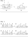
- FIG. 1(a) A general method for forming bumps by the electroplating method will be described with reference to FIG. 1 .
- a solder resist pattern having an opening is formed by lithography using a solder resist, on a surface of a substrate 1 on which wiring or the like is provided.
- a copper seed layer 3 for supplying electricity is formed on a surface of a solder resist layer 2 by electroless plating.
- a dry film resist layer 4 is formed on a surface of the copper seed layer 3, and a dry film resist pattern having an opening is formed so as to be connected to the opening of the solder resist layer 2.
- tin electroplating is performed in a via 6 of the dry film resist pattern, and a tin plating deposition layer 7 (tin plated film) is formed on the copper seed layer 3 in the via 6.
- the dry film resist layer 4 and the copper seed layer 3 are sequentially removed, and subsequently, the remaining tin plating deposition layer 7 is melted by a reflow process, and a tin bump 8 is formed as shown in FIG. 1(b) .
- Patent Document 1 discloses a tin or tin-alloy plating liquid containing a compound of specific ⁇ , ⁇ -unsaturated aldehyde or specific ⁇ , ⁇ -unsaturated ketone. The following matters are described in Patent Document 1.
- This plating liquid has high via filling property.
- tin plating is selectively deposited in recesses, a tin plating deposit having substantially no voids is obtained.
- a tin plated film Since no tinting or abnormal deposition occurs on a surface of the formed tin plated film, a tin plated film is obtained that is excellent in solderability and discoloration resistance and has a practical and good appearance.
- this plating liquid has high via filling property, it is possible to form a columnar tin plating deposit (bump) having substantially no voids.
- Patent Document 2 discloses a tin or tin-alloy plating liquid including (a) a carboxyl group-containing compound, and (b) a carbonyl group-containing compound, wherein the amount of the component (a) is 1.3 g/L or more, and the amount of the component (b) is 0.3 g/L or more. The following matters are described in Patent Document 2.
- the blind vias or the through holes can be filled with high reliability in a short amount of time.
- the plating liquid can be used for three-dimensional mounting of semiconductors, a step of filling blind vias or through holes in a printed wiring board, or a formation of silicon through electrodes.
- Patent Document 3 discloses a tin or tin-alloy plating liquid containing inorganic acid, organic acid, and a water-soluble salt thereof, a surfactant, and a leveling agent.
- the surfactant is at least one nonionic surfactant selected from the group consisting of polyoxyalkylene phenyl ethers or salts thereof and polyoxyalkylene polycyclic phenyl ethers or salts thereof.
- the phenyl forming the polyoxyalkylene phenyl ether and the polycyclic phenyl forming the polyoxyalkylene polycyclic phenyl ether may be substituted with an alkyl group having 1 to 24 carbon atoms or a hydroxy group.
- the leveling agent is at least one selected from the group consisting of aliphatic aldehydes, aromatic aldehydes, aliphatic ketones, and aromatic ketones; and ⁇ , ⁇ -unsaturated carboxylic acids, or amides thereof or salts thereof.
- the following matters are described in Patent Document 3.
- Patent Document 4 discloses a tin or tin-alloy electroplating liquid for forming bump electrodes, containing (A) a soluble salt consisting of either one of a stannous salt or a mixture of a stannous salt and a salt of a metal selected from silver, copper, bismuth, nickel, indium, and gold, (B) acid or a salt thereof, (C) a filling organic compound selected from the group consisting of aromatic and aliphatic aldehydes, aromatic and aliphatic ketones, unsaturated carboxylic acids, and aromatic carboxylic acids, and (D) a nonionic surfactant.
- A a soluble salt consisting of either one of a stannous salt or a mixture of a stannous salt and a salt of a metal selected from silver, copper, bismuth, nickel, indium, and gold
- B acid or a salt thereof
- C a filling organic compound selected from the group consisting of aromatic and aliphatic aldehy
- the component (D) is used in combination with the specific compound (C) that suppresses precipitation of a tin material, it is possible to effectively suppress the deposition on the upper part of the via and to advance the deposition of the tin material from the bottom of the via preferentially toward the upper part of the via. Therefore, it is possible to smoothly fill the via while preventing the occurrence of voids.
- the bump electrodes can be favorably formed with or without reflow, and the bonding strength and electrical characteristics are excellent.
- plating with a conventional tin or tin-alloy plating liquid can improve the via filling property of either one of a small diameter or a large diameter, but the via filling property of the other is reduced. That is, in a case of performing the plating on both vias 6 at the same time on a substrate having both vias 6 having a small diameter and a large diameter, it is difficult to perform the plating on both vias 6 with excellent via filling properties. As described above, in a case where vias 6 having different via filling properties are present ( FIG.
- An object of the invention is to provide a tin or tin-alloy plating liquid which has an excellent via filling property for vias on a substrate even in a pattern having different bump diameters, and which can form bumps having a uniform height.
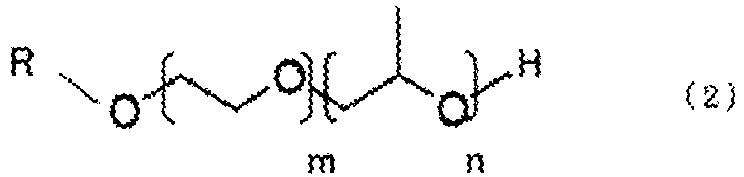
- a first aspect of the present invention is a tin or tin-alloy plating liquid containing: (A) a soluble salt including at least a stannous salt; (B) an acid selected from an organic acid and an inorganic acid, or a salt thereof; (C) a surfactant; (D) a leveling agent; and (E) an additive, wherein the surfactant is a compound (C1) represented by Formula (1) and/or a compound (C2) represented by Formula (2).
- R is an alkyl group having 7 to 13 carbon atoms, m is 5 to 11, n is 0 to 3, and m and n are different from each other.
- R is an alkyl group having 7 to 13 carbon atoms, m is 5 to 11, n is 1 to 3, and m and n are different from each other.
- a second aspect of the present invention is the tin or tin-alloy plating liquid according to the first aspect, wherein the additive contains two or more selected from a surfactant other than the two surfactants (C1 and C2), an antioxidant, and an alcohol having 1 to 3 carbon atoms.
- a third aspect of the present invention is a method for forming bumps including: a step of forming tin or tin-alloy plating deposition layers on a substrate using the tin or tin-alloy plating liquid according to the first or second aspect; and a step of subsequently performing a reflow process to form bumps.
- a fourth aspect of the present invention is a method for producing a circuit board including: producing a circuit board using the bumps formed by the method according to the third aspect.
- the surfactants (C1 and C2) have specific nonionic structure in which the number n of polyoxypropylene alkyl groups and the number m of polyoxyethylene groups in Formulas (1) and (2) are set to be in the predetermined ranges, respectively. Accordingly, at the time of plating, it is possible to suppress precipitation of Sn ions and perform good plating on a surface to be plated.
- this plating liquid in a case of a pattern having different bump diameters, although the bump diameter is large or small, the via filling property for vias on a substrate are excellent, and heights of formed bumps become uniform. It is considered that this is because the polarization resistance increases.
- a surfactant other than the two surfactants (C1 and C2), an antioxidant, and an alcohol having 1 to 3 carbon atoms are further contained; and thereby, the following effects are exhibited.
- the surfactant other than the two surfactants (C1 and C2) exhibits effects such as stabilization of the plating liquid, improvement of solubility, and the like.
- the antioxidant prevents the oxidation of a soluble stannous salt to a stannic salt.
- the alcohol exhibits an effect of improving the solubility of the surfactant.
- the tin or tin-alloy plating deposition layers are formed on a substrate using the tin or tin-alloy plating liquid according to the first or second aspect, and next, a reflow process is performed to form bumps. Accordingly, it is possible to form bumps having a uniform height even in a pattern having different bump diameters.
- a circuit board is produced using the bumps formed by the method according to the third aspect. Accordingly, a highly reliable semiconductor device without electrical connection failure can be produced.
- FIG. 1(a) is a cross-sectional view of a substrate in which a plating deposition layer is formed in a via, according to the present embodiment.
- FIG. 1(b) is a cross-sectional view of the substrate, after peeling a dry film and a copper seed layer and heating the plating deposition layer.
- FIG. 2(a) is a cross-sectional configuration diagram of a substrate showing an example in which plating deposition layers have good via filling property in a pattern having different bump diameters (via diameters).
- FIG. 2(b) is a cross-sectional configuration diagram of a substrate showing an example in which plating deposition layers have poor via filling property in a pattern having different bump diameters (via diameters).
- FIG. 2(c) is a cross-sectional configuration diagram of a substrate which is in a state after peeling a dry film and a copper seed layer in FIG. 2(a) and heating the plating deposition layers and shows an example in which heights of formed bumps are uniform.
- FIG. 2(d) is a cross-sectional configuration diagram of a substrate which is in a state after peeling a dry film and a copper seed layer in FIG. 2(b) and heating the plating deposition layer and shows an example in which heights of formed bumps vary.
- a tin or tin-alloy plating liquid of the present embodiment contains (A) a soluble salt including at least a stannous salt, (B) an acid selected from an organic acid and an inorganic acid, or a salt thereof, (C) a surfactant, (D) a leveling agent, and (E) an additive.
- the remainder is water of a solvent.
- the surfactant is the compound (C1) represented by Formula (1) and/or the compound (C2) represented by Formula (2).
- the soluble salt includes either one of a stannous salt or a mixture of the stannous salt and a salt of a metal selected from silver, copper, bismuth, nickel, antimony, indium, and zinc.
- the tin alloy of the present embodiment is an alloy of tin and a predetermined metal selected from silver, copper, bismuth, nickel, antimony, indium, and zinc, and examples thereof include a tin-silver alloy, a tin-copper alloy, a tin-bismuth alloy, a tin-nickel alloy, a tin-antimony alloy, a tin-indium alloy, a binary alloy of a tin-zinc alloy, and a ternary alloy such as a tin-copper-bismuth alloy or tin-copper-silver alloy.
- the soluble salt (A) of the present embodiment means any soluble salt that generates various metal ions such as Sn 2+ , Ag + , Cu + , Cu 2+ , Bi 3+ , Ni 2+ , Sb 3+ , In 3+ , and Zn 2+ in the plating liquid, and examples thereof include an oxide and a halide of the metal, and the metal salt of inorganic acid or organic acid.
- Examples of the oxide of the metal include a stannous oxide, a copper oxide, a nickel oxide, a bismuth oxide, an antimony oxide, an indium oxide, and a zinc oxide.
- Examples of the halide of the metal include a stannous chloride, a bismuth chloride, a bismuth bromide, a cuprous chloride, a cupric chloride, a nickel chloride, an antimony chloride, an indium chloride, and a zinc chloride.
- Examples of the metal salt of inorganic acid or organic acid include copper sulfate, stannous sulfate, bismuth sulfate, nickel sulfate, antimony sulfate, bismuth nitrate, silver nitrate, a copper nitrate, antimony nitrate, indium nitrate, nickel nitrate, zinc nitrate, copper acetate, nickel acetate, nickel carbonate, sodium stannate, stannous borofluoride, stannous methanesulfonate, silver methanesulfonate, copper methanesulfonate, bismuth methanesulfonate, nickel methanesulfonate, indium methanesulfonate, zinc bis(methanesulfonate), stannous ethanesulfonate, and bismuth 2-hydroxypropanesulfonate.
- the acid or the salt thereof (B) of the present embodiment is selected from an organic acid, an inorganic acid, and a salt thereof.
- the organic acid include an organic sulfonic acid such as an alkane sulfonic acid, an alkanol sulfonic acid, and an aromatic sulfonic acid, or an aliphatic carboxylic acid.
- the inorganic acid include a borofluoric acid, a hydrosilicofluoric acid, a sulfamic acid, a hydrochloric acid, a sulfuric acid, a nitric acid, and a perchloric acid.
- the salt thereof examples include a salt of alkali metal, a salt of alkaline earth metal, an ammonium salt, an amine salt, and a sulfonate.
- the component (B) is preferably the organic sulfonic acid from a viewpoint of solubility of the metal salt or ease of wastewater treatment.
- the aromatic sulfonic acid is basically benzene sulfonic acid, alkyl benzene sulfonic acid, phenol sulfonic acid, naphthalene sulfonic acid, or alkyl naphthalene sulfonic acid, and specific examples thereof include 1-naphthalene sulfonic acid, 2-naphthalene sulfonic acid, toluenesulfonic acid, xylenesulfonic acid, p-phenolsulfonic acid, cresolsulfonic acid, sulfosalicylic acid, nitrobenzenesulfonic acid, sulfobenzoic acid, and diphenylamine-4-sulfonic acid.
- aliphatic carboxylic acid examples include acetic acid, propionic acid, butyric acid, citric acid, tartaric acid, gluconic acid, sulfosuccinic acid, and trifluoroacetic acid.
- the nonionic surfactant (C1) included as the surfactant (C) of the present embodiment is a condensate of polyoxyethylene and polyoxypropylene alkyl ether or polyoxyethylene alkyl ether, represented by the following Formula (1).
- R is an alkyl group having 7 to 13 carbon atoms, m is 5 to 11, n is 0 to 3, and m and n are different from each other.
- the alkyl group of R may be linear or may have a branched chain.
- the carbon number of R is less than 7, there is a problem that the appearance of plating is abnormal.
- the carbon number of R exceeds 13, there is a problem that it is difficult to dissolve in the plating liquid, the via filling property is poor, or the appearance of plating is abnormal.
- the carbon number of R is preferably 10 to 12.
- m is less than 5
- n is preferably 0 to 2.
- the nonionic surfactant (C2) included as the surfactant (C) of the present embodiment is a condensate of polyoxypropylene and polyoxyethylene alkyl ether, represented by the following Formula (2).
- R is an alkyl group having 7 to 13 carbon atoms, m is 5 to 11, n is 1 to 3, and m and n are different from each other.
- the alkyl group of R may be linear or may have a branched chain.
- the carbon number of R is less than 7, there is a problem that the appearance of plating is abnormal.
- the carbon number of R exceeds 13, there is a problem that it is difficult to dissolve in the plating liquid, the via filling property is poor, or the appearance of plating is abnormal.
- the carbon number of R is preferably 10 to 12.
- m is less than 5
- n is preferably 1 to 2.
- the leveling agent (D) of the present embodiment is added to form a uniform and dense plated film and to smooth the plated film.
- a first leveling agent (D-1) and a second leveling agent (D-2) are used.
- the first leveling agent (D-1) include one or more selected from the group consisting of aliphatic aldehyde, aromatic aldehyde, aliphatic ketone, and aromatic ketone
- examples of the second leveling agent (D-2) include ⁇ , ⁇ -unsaturated carboxylic acid, amides thereof, and salts thereof.
- the first leveling agent (D-1) is a carbonyl compound containing aldehyde or ketone, and does not include the ⁇ , ⁇ -unsaturated carboxylic acid of the second leveling agent (D-2). Specific examples are as follows. Examples of the aliphatic aldehyde include formaldehyde, acetaldehyde, and allyl aldehyde.
- aromatic aldehyde examples include benzaldehyde, 2-chlorobenzaldehyde, 3-chlorobenzaldehyde, 4-chlorobenzaldehyde, 2,4-dichlorobenzaldehyde, 2,6-dichlorobenzaldehyde, 2,4,6-trichlorobenzaldehyde, 1 -naphthaldehyde, 2-naphthaldehyde, 2-hydroxybenzaldehyde, 3 -hydroxybenzaldehyde, 4-hydroxybenzaldehyde, 2-methylbenzaldehyde, 3-methylbenzaldehyde, 4-methylbenzaldehyde, m-anisaldehyde, o-anisaldehyde, and p-anisaldehyde.
- examples of the aliphatic ketone include acetylacetone.
- examples of the aromatic ketone include benzylideneacetone (synonymous with benzalacetone), 2-chloroacetophenone, 3-chloroacetophenone, 4-chloroacetophenone, 2,4-dichloroacetophenone, and 2,4,6-trichloroacetophenone.
- benzylideneacetone synonymous with benzalacetone
- 2-chloroacetophenone 2-chloroacetophenone
- 3-chloroacetophenone 4-chloroacetophenone
- 2,4-dichloroacetophenone 2,4,6-trichloroacetophenone
- a preferable amount of the first leveling agent (D-1) in an electroplating bath is 0.001 g/L to 0.3 g/L and more preferably 0.01 g/L to 0.25 g/L.
- the amount of the component is small, the effect of adding the component is not sufficient, and on the other hand, in a case where the amount of the component is excessively large, the smoothing of the plated film may be inhibited.
- Examples of the second leveling agent (D-2) include acrylic acid, methacrylic acid, picolinic acid, crotonic acid, 3-chloroacrylic acid, 3,3-dimethylacrylic acid, 2,3-dimethylacrylic acid, methyl acrylate, ethyl acrylate, n-butyl acrylate, isobutyl acrylate, 2-ethylhexyl acrylate, ethyl methacrylate, n-butyl methacrylate, isobutyl methacrylate, 2-hydroxyethyl methacrylate, 2-hydroxypropyl methacrylate, 2-dimethylaminoethyl methacrylate, methacrylic anhydride, and methyl methacrylic acid.
- the second leveling agent (D-2) also includes amide of ⁇ , ⁇ -unsaturated carboxylic acid (for example, acrylamide or the like) and a salt of ⁇ , ⁇ -unsaturated carboxylic acid (for example, salt of potassium, sodium, or ammonium).
- a preferable amount of the second leveling agent (D-2) in an electroplating bath is 0.01 g/L to 50 g/L and more preferably 0.05 g/L to 10 g/L. In a case where the amount of the component is small, the effect of adding the component is not sufficient, and on the other hand, in a case where the amount of the component is excessively large, the smoothing of the plated film may be inhibited.
- the additive (E) of the present embodiment is various additives added to the tin or tin-alloy plating liquid.
- the additive (E) preferably includes two or more selected from a surfactant other than the two surfactants (C1 and C2) described above, an antioxidant, and an alcohol having 1 to 3 carbon atoms.
- examples of the other surfactant include an ordinary anionic surfactant, a cationic surfactant, a nonionic surfactant, and an amphoteric surfactant.
- anionic surfactant examples include polyoxyalkylene alkyl ether sulfate such as sodium polyoxyethylene (containing 12 mol of ethylene oxide in 1 mol of molecule) nonyl ether sulfate; polyoxyalkylene alkyl phenyl ether sulfate such as sodium polyoxyethylene (containing 12 mol of ethylene oxide in 1 mol of molecule) dodecylphenyl ether sulfate; alkyl benzene sulfonate such as sodium dodecylbenzene sulfonate; naphthol sulfonate such as sodium 1-naphthol-4-sulfonate or disodium 2-naphthol-3,6-disulfonate; (poly)alkylnaphthalenesulfonate such as sodium diisopropylnaphthalenesulfonate or sodium dibutylnaphthalenesulfonate; and alkyl sul
- cationic surfactant examples include monoalkylamine salt, dialkylamine salt, trialkylamine salt, dimethyldialkylammonium salt, trimethylalkylammonium salt, dodecyltrimethylammonium salt, hexadecyltrimethylammonium salt, octadecyltrimethylammonium salt, dodecyldimethylammonium salt, octadecenyl dimethylethylammonium salt, dodecyldimethylbenzylammonium salt, hexadecyldimethylbenzylammonium salt, octadecyldimethylbenzylammonium salt, trimethylbenzylammonium salt, triethylbenzylammonium salt, hexadecylpyridinium salt, dodecylpyridinium salt, dodecylpicolinium salt, dodecylimidazolinium salt, oleyl imi
- nonionic surfactant examples include sugar ester, fatty acid ester, C 1 to C 25 alkoxyl phosphoric acid (salt), sorbitan ester, silicon-based polyoxyethylene ether, silicon-based polyoxyethylene ester, fluorine-based polyoxyethylene ether, fluorine-based polyoxyethylene ester, a sulfated or sulfonated adduct of a condensation product of ethylene oxide and/or propylene oxide and an alkylamine or diamine, and polyoxyethylene cumyl phenyl ether (however, EO chain is 10 to 14).
- amphoteric surfactant examples include betaine, carboxybetaine, imidazolinium betaine, sulfobetaine, and aminocarboxylic acid.
- the antioxidant is used for preventing the oxidation of the soluble stannous salt to the stannic salt.
- antioxidant examples include hypophosphorous acids, ascorbic acid or a salt thereof, phenolsulfonic acid (Na), cresolsulfonic acid (Na), hydroquinonesulfonic acid (Na), hydroquinone, ⁇ - or ⁇ -naphthol, catechol, resorcin, phloroglucin, hydrazine, phenolsulfonic acid, catecholsulfonic acid, hydroxybenzenesulfonic acid, naphtholsulfonic acid, and salts thereof.
- the alcohol having 1 to 3 carbon atoms is used for improving the solubility of the surfactant.
- examples of the alcohol include methanol, ethanol, 1-propanol, and 2-propanol.
- One of the alcohols can be used alone or a combination of two or more thereof can be used.
- the amount of the nonionic surfactant (C1 or C2) in the plating liquid is 0.5 g/L to 50 g/L, and preferably 1 g/L to 5 g/L. In a case where the amount is less than the lower limit, plating failure such as a dendrite occurs due to an excessive supply of Sn ions. In addition, in a case where the amount exceeds the upper limit, Sn ions hardly reach a surface to be plated, and the via filling property may deteriorate.
- the total amount of the nonionic surfactant (C1) and the amount of the nonionic surfactant (C2) may be set to be in the above-described range.
- the soluble metal salt (A) one of the compounds can be used alone or a combination of two or more thereof can be used, and an amount in the plating liquid is 30 g/L to 100 g/L, and preferably 40 g/L to 60 g/L. In a case where the amount is less than the appropriate range, the productivity is reduced, and in a case where the amount increases, the cost of the plating liquid increases.
- the inorganic acid, the organic acid, or the salt thereof (B) only one kind or two or more kinds of the compounds can be used, and an amount thereof in the plating liquid is 80 to 300 g/L, and preferably 100 to 200 g/L. In a case where the amount is less than the appropriate range, conductivity is low and voltage rises. In a case where the amount is more than the appropriate range, viscosity of the plating liquid increases and stirring speed of the plating liquid decreases.
- the amount of the additive (E) in the plating liquid is 0.5 g/L to 50 g/L and preferably 1 g/L to 5 g/L.
- the temperature of the electroplating liquid of the present embodiment is generally 70°C or lower, and preferably 10°C to 40°C.
- the current density during the formation of a plated film by electroplating is in a range of 0.1 A/dm 2 to 100 A/dm 2 and preferably in a range of 0.5 A/dm 2 to 20 A/dm 2 . In a case where the current density is excessively low, the productivity deteriorates, and in a case where the current density is excessively high, the height uniformity of the bumps deteriorates.
- the tin or tin-alloy plating liquid of the present embodiment containing the nonionic surfactant (C1 and/or C2) alone or both of the nonionic surfactant (C1) and the nonionic surfactant (C2) as the surfactant is applied to a circuit board serving as an object to be plated, and the liquid temperature and the current density are set to be within the ranges, a predetermined metal film (tin or tin-alloy plating deposition layer) can be formed on the circuit board. Then, when a reflow process is performed, bumps are formed.
- Examples of the circuit board include a printed circuit board, a flexible printed circuit board, and a semiconductor integrated circuit board.
- Nonionic surfactant (C1) used in Examples and Comparative Examples
- Table 1 shows the carbon number of R, the number m of the polyoxyethylene (EO) group, and the number n of the polyoxypropylene (PO) group in each Structural Formula (1) of condensates of polyoxyethylene and polyoxypropylene alkyl ether or polyoxyethylene alkyl ethers (C1-1 to C1-17) which are nonionic surfactants (C1) used in Examples 1 to 8, 13, and 14 and Comparative Examples 1 to 10.
- Nonionic surfactant (C2) used in Examples and Comparative Examples
- Table 2 shows the carbon number of R, the number m of the polyoxyethylene (EO) group, and the number n of the polyoxypropylene (PO) group in each Structural Formula (1) of condensates of polyoxypropylene and polyoxyethylene alkyl ether which are nonionic surfactants (C2) used in Examples 1, 2, and 9 to 14, and Comparative Examples 11 to 16 (C2-1 to C2-10).
- C2 nonionic surfactants
- Nonionic surfactant compound (C1) Compound (C1) Carbon number of R m (EO group) number n (PO group) number Mass average molecular weight C1-1 7 2 0 270 C1-2 16 3 0 350 C1-3 7 4 0 430 C1-4 6 5 0 380 C1-5 7 5 0 350 C1-6 13 6 0 500 C1-7 13 7 0 520 C1-8 7 11 1 750 C1-9 9 6 2 530 C1-10 13 8 2 650 C1-11 9 8 3 700 C1-12 16 10 3 890 C1-13 8 13 3 930 C1-14 16 15 3 1200 C1-15 8 15 4 1100 C1-16 16 8 4 850 C1-17 9 8 4 750 Table 2 Nonionic surfactant compound (C2) No.
- Methanesulfonic acid as a free acid, hydroquinone as an antioxidant, 1-naphthaldehyde as a leveling agent (D-1), methacrylic acid as a leveling agent (D-2) were mixed with a Sn methanesulfonate aqueous solution to obtain a homogeneous solution.
- D-1 1-naphthaldehyde
- D-2 methacrylic acid as a leveling agent
- C2-2 condensate of polyoxyethylene and polyoxypropylene alkyl ether (mass average molecular weight: 530, carbon number in R in Formula (2): 9, number m of polyoxyethylene (EO) groups: 6, and number n of polyoxypropylene (PO) groups: 2) were added.
- Ion-exchanged water was finally added to initially make-up a Sn plating liquid having the following composition.
- the Sn methanesulfonate aqueous solution was prepared by electrolyzing a metal Sn plate in a methanesulfonic acid aqueous solution.
- Methanesulfonic acid as a free acid, catechol as an antioxidant, benzaldehyde as the leveling agent (D-1), methyl methacrylic acid as the leveling agent (D-2) were mixed with the Sn methanesulfonate aqueous solution to dissolve. Further, an Ag methanesulfonate liquid was added and mixed. A homogeneous solution was obtained by mixing. Then, as a surfactant, the above No.
- the Sn methanesulfonate aqueous solution was prepared by electrolyzing a Sn metal plate in a methanesulfonic acid aqueous solution, and the Ag methanesulfonate aqueous solution was prepared by electrolyzing the Ag metal plate in a methanesulfonic acid aqueous solution.
- Examples 6 and 13 and Comparative Examples 3, 8, and 11 as the nonionic surfactant (C1) and the nonionic surfactant (C2), the surfactants having the properties shown in Tables 1 and 2 were used and selected as shown in Tables 3 and 4. Except for this, in the same manner as in Example 2, SnAg plating liquids of Examples 6 and 13 and Comparative Examples 3, 8, and 11 were initially made-up.
- Methanesulfonic acid as a free acid, potassium hydroquinone sulfonate as an antioxidant, benzaldehyde as the leveling agent (D-1), methyl methacrylic acid as the leveling agent (D-2) were mixed with the Sn methanesulfonate aqueous solution to dissolve.
- Cu methanesulfonate liquid was further added and mixed. A homogeneous solution was obtained by mixing.
- the No. C2-4 condensate of polyoxyethylene and polyoxypropylene (mass average molecular weight: 700, carbon number of R in Formula (2): 9, number m of polyoxyethylene (EO) groups: 8, number n of polyoxypropylene (PO) groups: 3) was added.
- SnCu plating liquid having the following composition.
- the Sn methanesulfonate aqueous solution was prepared by electrolyzing a Sn metal plate in a methanesulfonic acid aqueous solution
- the Cu methanesulfonate aqueous solution was prepared by electrolyzing the Cu metal plate in a methanesulfonic acid aqueous solution.
- Comparative Examples 6 and 14 as the surfactant, surfactants having the properties shown in Table 2 were used and selected as shown in Table 4. Except for this, in the same manner as in Example 10, SnCu plating liquids of Comparative Examples 6 and 14 were initially made-up.
- the tin or tin-alloy plating deposition layers in the vias were observed with a laser microscope, and a difference in height between the highest point and the lowest point of the plating deposition layer was measured. A case where the difference in height exceeded 5 ⁇ m was determined to be “poor”, a case where the difference in height was 5 ⁇ m or less was determined to be “good”, and these are shown in the "via filling property" column of Tables 3 and 4.
- the tin or tin-alloy plating deposition layers in the vias were observed with a laser microscope, and a surface roughness Ra was measured.
- a case where the surface roughness Ra of the plating deposition layer exceeded 2 ⁇ m was determined to be “poor”
- a case where the surface roughness Ra was 2 ⁇ m or less was determined to be “good”
- these are shown in the "appearance of plating deposition layer" column of Tables 3 and 4.
- the heights of the bumps on the substrate were measured using an automatic appearance inspection device. A variation in heights was calculated from the measured bump heights. A case where the height variation was 3 or less was determined to be “uniform”, a case where the height variation exceeded 3 was determined to be “non-uniform", and the results are shown in the "bump height variation” column of Tables 3 and 4.
- Bumps (2000 bumps in total) arranged at pitch intervals of 180 ⁇ m, 250 ⁇ m, and 360 ⁇ m and having diameters of 70 ⁇ m, 90 ⁇ m, and 120 ⁇ m were formed. Transmission X-ray images of these bumps were captured. The captured image was visually observed. A case where one or more voids having a size of 1 % or more of the size of the bump was observed was determined to be "NG", and a case where no voids were observed was determined to be "OK”. The results thereof are shown in the "void" column of Tables 3 and 4.
- Nonionic surfactant compound (C1) Nonionic surfactant compound (C2) Metal other than Sn Evaluation Via filling property Appearance of plating deposition layer Bump height variation Void Compound No. Carbon number of R EO groups m PO groups n Compound No.
- the carbon numbers of R were in the range of 7 to 13
- the numbers m of EO groups were in the range of 5 to 11
- the numbers n of PO groups were 0 to 3
- the height variations of the bumps were in the range of 1.0 to 2.6 which were small, and no voids were observed in all which were determined to be OK.
- the tin or tin-alloy plating liquid of the embodiment can be used for a circuit board such as a printed circuit board, a flexible printed circuit board, and a semiconductor integrated circuit.
Landscapes
- Chemical & Material Sciences (AREA)
- Engineering & Computer Science (AREA)
- Chemical Kinetics & Catalysis (AREA)
- Electrochemistry (AREA)
- Materials Engineering (AREA)
- Metallurgy (AREA)
- Organic Chemistry (AREA)
- Manufacturing & Machinery (AREA)
- Microelectronics & Electronic Packaging (AREA)
- Electroplating And Plating Baths Therefor (AREA)
- Electroplating Methods And Accessories (AREA)
Abstract

Description
- The present invention relates to a tin or tin-alloy plating liquid for producing bumps serving as bump electrodes of tin or a tin alloy on a substrate when mounting a semiconductor integrated circuit chip on a circuit board, a method for forming bumps (a bump forming method) using the same, and a method for producing a circuit board (a circuit board production method). The invention more particularly relates to a tin or tin-alloy plating liquid which has excellent via filling property for vias on a substrate even in a pattern having different bump diameters or bump pitches, and which can form bumps having a uniform height.
- The present application claims priority on Japanese Patent Application No.
2018-52012 filed on March 20, 2018 2018-57551 filed on March 26, 2018 2019-40216 filed on March 6, 2019 - In a circuit board on which a semiconductor integrated circuit chip (hereinafter, referred to as a semiconductor chip) is to be mounted, a chip size/scale package (CSP) type semiconductor device having a package substrate area that is reduced to approximately the same size as that of a semiconductor chip to be mounted on the substrate is currently mainly produced, in order to support lightness, thinness, shortness, and smallness (lightening, thinning, and miniaturization). In order to connect the circuit board and the semiconductor chip to each other, via openings which are via bodies on a substrate side are filled with tin or a tin alloy to form bumps which are bump electrodes of protruding metal terminals, and these bumps are loaded with a semiconductor chip.
- In the related art, in a case of forming bumps by the filling of the tin or tin alloy material, the via bodies are filled with a conductive paste such as a tin-based solder paste or tin-based solder balls, or tin-plating deposition layers are formed in the vias by an electroplating method using a tin or tin-alloy plating liquid, and subsequently, the conductive paste, the solder balls, or the tin plating deposition layers are melted by a heat treatment.
- A general method for forming bumps by the electroplating method will be described with reference to
FIG. 1 . As shown inFIG. 1(a) , a solder resist pattern having an opening is formed by lithography using a solder resist, on a surface of asubstrate 1 on which wiring or the like is provided. Next, acopper seed layer 3 for supplying electricity is formed on a surface of asolder resist layer 2 by electroless plating. Next, a dryfilm resist layer 4 is formed on a surface of thecopper seed layer 3, and a dry film resist pattern having an opening is formed so as to be connected to the opening of thesolder resist layer 2. Next, by supplying electricity through thecopper seed layer 3, tin electroplating is performed in avia 6 of the dry film resist pattern, and a tin plating deposition layer 7 (tin plated film) is formed on thecopper seed layer 3 in thevia 6. Next, the dryfilm resist layer 4 and thecopper seed layer 3 are sequentially removed, and subsequently, the remaining tinplating deposition layer 7 is melted by a reflow process, and atin bump 8 is formed as shown inFIG. 1(b) . - Previously, in a case of forming tin or tin alloy bumps using the electroplating method, the improvement regarding via filling property of vias on the substrate or prevention of voids in the bumps has been made by changing the components included in the tin or tin-alloy plating liquid (for example, see
Patent Documents -
Patent Document 1 discloses a tin or tin-alloy plating liquid containing a compound of specific α,β-unsaturated aldehyde or specific α,β-unsaturated ketone. The following matters are described inPatent Document 1. - This plating liquid has high via filling property. When this plating liquid is used, since tin plating is selectively deposited in recesses, a tin plating deposit having substantially no voids is obtained.
- Since no tinting or abnormal deposition occurs on a surface of the formed tin plated film, a tin plated film is obtained that is excellent in solderability and discoloration resistance and has a practical and good appearance.
- Since this plating liquid has high via filling property, it is possible to form a columnar tin plating deposit (bump) having substantially no voids.
-
Patent Document 2 discloses a tin or tin-alloy plating liquid including (a) a carboxyl group-containing compound, and (b) a carbonyl group-containing compound, wherein the amount of the component (a) is 1.3 g/L or more, and the amount of the component (b) is 0.3 g/L or more. The following matters are described inPatent Document 2. - By electroplating an object to be plated having blind vias or through holes using this plating liquid, the blind vias or the through holes can be filled with high reliability in a short amount of time.
- The plating liquid can be used for three-dimensional mounting of semiconductors, a step of filling blind vias or through holes in a printed wiring board, or a formation of silicon through electrodes.
-
Patent Document 3 discloses a tin or tin-alloy plating liquid containing inorganic acid, organic acid, and a water-soluble salt thereof, a surfactant, and a leveling agent. The surfactant is at least one nonionic surfactant selected from the group consisting of polyoxyalkylene phenyl ethers or salts thereof and polyoxyalkylene polycyclic phenyl ethers or salts thereof. The phenyl forming the polyoxyalkylene phenyl ether and the polycyclic phenyl forming the polyoxyalkylene polycyclic phenyl ether may be substituted with an alkyl group having 1 to 24 carbon atoms or a hydroxy group. The leveling agent is at least one selected from the group consisting of aliphatic aldehydes, aromatic aldehydes, aliphatic ketones, and aromatic ketones; and α,β-unsaturated carboxylic acids, or amides thereof or salts thereof. The following matters are described inPatent Document 3. - Since a specific nonionic surfactant and two specific leveling agents are contained, recess filling property is excellent and it is possible to suppress the occurrence of voids. As a result, by using this plating liquid, it is possible to provide good bumps that are smooth without recesses and do not generate voids after reflow.
- Further,
Patent Document 4 discloses a tin or tin-alloy electroplating liquid for forming bump electrodes, containing (A) a soluble salt consisting of either one of a stannous salt or a mixture of a stannous salt and a salt of a metal selected from silver, copper, bismuth, nickel, indium, and gold, (B) acid or a salt thereof, (C) a filling organic compound selected from the group consisting of aromatic and aliphatic aldehydes, aromatic and aliphatic ketones, unsaturated carboxylic acids, and aromatic carboxylic acids, and (D) a nonionic surfactant. The following matters are described inPatent Document 4. - Since in this plating liquid, the component (D) is used in combination with the specific compound (C) that suppresses precipitation of a tin material, it is possible to effectively suppress the deposition on the upper part of the via and to advance the deposition of the tin material from the bottom of the via preferentially toward the upper part of the via. Therefore, it is possible to smoothly fill the via while preventing the occurrence of voids. As a result, the bump electrodes can be favorably formed with or without reflow, and the bonding strength and electrical characteristics are excellent.
- In recent years, wiring patterns having different bump diameters or bump pitches have been mixed on one circuit board. In such complicated wiring patterns, it is necessary to form all bumps at a uniform height, even in a case where the bump diameters and the bump pitches are different. According to the tin or tin-alloy plating liquids of
Patent Documents 1 to 4, there are advantages that the occurrence of voids in the bumps is prevented, the vias on the substrate can be filled with high reliability in a short period of time, and the via filling property and appearance are excellent. However, the plating liquids for substrates inPatent Documents 1 to 4 do not aim at achieving bump height uniformity. - Specifically, as shown in
FIG. 2 , in the case of a pattern having different bump diameters, plating with a conventional tin or tin-alloy plating liquid can improve the via filling property of either one of a small diameter or a large diameter, but the via filling property of the other is reduced. That is, in a case of performing the plating on bothvias 6 at the same time on a substrate having bothvias 6 having a small diameter and a large diameter, it is difficult to perform the plating on bothvias 6 with excellent via filling properties. As described above, in a case wherevias 6 having different via filling properties are present (FIG. 2(b) ), a variation in height of thebumps 8 after the reflow increases, and height uniformity of thebumps 8 cannot be achieved (FIG. 2(d) ). Therefore, in order to achieve the height uniformity of the bumps 8 (FIG. 2(c) ), as shown inFIG. 2(a) , it is necessary to improve via filling properties for bothvias 6 having a small diameter and a large diameter. -
- Patent Document 1: Japanese Unexamined Patent Application, First Publication No.
2014-125662 claim 2, paragraph [0020]) - Patent Document 2: Japanese Unexamined Patent Application, First Publication No.
2015-007276 claim 1, paragraphs [0011] and [0012]) - Patent Document 3: Japanese Unexamined Patent Application, First Publication No.
2015-193916 claim 1, paragraph [0019]) - Patent Document 4: Japanese Unexamined Patent Application, First Publication No.
2016-074963 claim 1, paragraph [0019]) - An object of the invention is to provide a tin or tin-alloy plating liquid which has an excellent via filling property for vias on a substrate even in a pattern having different bump diameters, and which can form bumps having a uniform height.
- A first aspect of the present invention is a tin or tin-alloy plating liquid containing: (A) a soluble salt including at least a stannous salt; (B) an acid selected from an organic acid and an inorganic acid, or a salt thereof; (C) a surfactant; (D) a leveling agent; and (E) an additive, wherein the surfactant is a compound (C1) represented by Formula (1) and/or a compound (C2) represented by Formula (2).
- In Formula (1), R is an alkyl group having 7 to 13 carbon atoms, m is 5 to 11, n is 0 to 3, and m and n are different from each other. In addition, in Formula (2), R is an alkyl group having 7 to 13 carbon atoms, m is 5 to 11, n is 1 to 3, and m and n are different from each other.


- A second aspect of the present invention is the tin or tin-alloy plating liquid according to the first aspect, wherein the additive contains two or more selected from a surfactant other than the two surfactants (C1 and C2), an antioxidant, and an alcohol having 1 to 3 carbon atoms.
- A third aspect of the present invention is a method for forming bumps including: a step of forming tin or tin-alloy plating deposition layers on a substrate using the tin or tin-alloy plating liquid according to the first or second aspect; and a step of subsequently performing a reflow process to form bumps.
- A fourth aspect of the present invention is a method for producing a circuit board including: producing a circuit board using the bumps formed by the method according to the third aspect.
- In the tin or tin-alloy plating liquid according to the first aspect of the present invention, the surfactants (C1 and C2) have specific nonionic structure in which the number n of polyoxypropylene alkyl groups and the number m of polyoxyethylene groups in Formulas (1) and (2) are set to be in the predetermined ranges, respectively. Accordingly, at the time of plating, it is possible to suppress precipitation of Sn ions and perform good plating on a surface to be plated. In particular, according to this plating liquid, in a case of a pattern having different bump diameters, although the bump diameter is large or small, the via filling property for vias on a substrate are excellent, and heights of formed bumps become uniform. It is considered that this is because the polarization resistance increases.
- In the tin or tin-alloy plating liquid according to the second aspect of the present invention, two or more selected from a surfactant other than the two surfactants (C1 and C2), an antioxidant, and an alcohol having 1 to 3 carbon atoms are further contained; and thereby, the following effects are exhibited. The surfactant other than the two surfactants (C1 and C2) exhibits effects such as stabilization of the plating liquid, improvement of solubility, and the like. In addition, the antioxidant prevents the oxidation of a soluble stannous salt to a stannic salt. Further, the alcohol exhibits an effect of improving the solubility of the surfactant.
- In the method according to the third aspect of the present invention, the tin or tin-alloy plating deposition layers are formed on a substrate using the tin or tin-alloy plating liquid according to the first or second aspect, and next, a reflow process is performed to form bumps. Accordingly, it is possible to form bumps having a uniform height even in a pattern having different bump diameters.
- In the method according to the fourth aspect of the present invention, a circuit board is produced using the bumps formed by the method according to the third aspect. Accordingly, a highly reliable semiconductor device without electrical connection failure can be produced.
-
FIG. 1(a) is a cross-sectional view of a substrate in which a plating deposition layer is formed in a via, according to the present embodiment.FIG. 1(b) is a cross-sectional view of the substrate, after peeling a dry film and a copper seed layer and heating the plating deposition layer. -
FIG. 2(a) is a cross-sectional configuration diagram of a substrate showing an example in which plating deposition layers have good via filling property in a pattern having different bump diameters (via diameters).FIG. 2(b) is a cross-sectional configuration diagram of a substrate showing an example in which plating deposition layers have poor via filling property in a pattern having different bump diameters (via diameters).FIG. 2(c) is a cross-sectional configuration diagram of a substrate which is in a state after peeling a dry film and a copper seed layer inFIG. 2(a) and heating the plating deposition layers and shows an example in which heights of formed bumps are uniform.FIG. 2(d) is a cross-sectional configuration diagram of a substrate which is in a state after peeling a dry film and a copper seed layer inFIG. 2(b) and heating the plating deposition layer and shows an example in which heights of formed bumps vary. - Next, an embodiment of the present invention will be described.
- A tin or tin-alloy plating liquid of the present embodiment contains (A) a soluble salt including at least a stannous salt, (B) an acid selected from an organic acid and an inorganic acid, or a salt thereof, (C) a surfactant, (D) a leveling agent, and (E) an additive. The remainder is water of a solvent. The surfactant is the compound (C1) represented by Formula (1) and/or the compound (C2) represented by Formula (2).
- The soluble salt includes either one of a stannous salt or a mixture of the stannous salt and a salt of a metal selected from silver, copper, bismuth, nickel, antimony, indium, and zinc.
- The tin alloy of the present embodiment is an alloy of tin and a predetermined metal selected from silver, copper, bismuth, nickel, antimony, indium, and zinc, and examples thereof include a tin-silver alloy, a tin-copper alloy, a tin-bismuth alloy, a tin-nickel alloy, a tin-antimony alloy, a tin-indium alloy, a binary alloy of a tin-zinc alloy, and a ternary alloy such as a tin-copper-bismuth alloy or tin-copper-silver alloy.
- Therefore, the soluble salt (A) of the present embodiment means any soluble salt that generates various metal ions such as Sn2+, Ag+, Cu+, Cu2+, Bi3+, Ni2+, Sb3+, In3+, and Zn2+ in the plating liquid, and examples thereof include an oxide and a halide of the metal, and the metal salt of inorganic acid or organic acid.
- Examples of the oxide of the metal include a stannous oxide, a copper oxide, a nickel oxide, a bismuth oxide, an antimony oxide, an indium oxide, and a zinc oxide. Examples of the halide of the metal include a stannous chloride, a bismuth chloride, a bismuth bromide, a cuprous chloride, a cupric chloride, a nickel chloride, an antimony chloride, an indium chloride, and a zinc chloride.
- Examples of the metal salt of inorganic acid or organic acid include copper sulfate, stannous sulfate, bismuth sulfate, nickel sulfate, antimony sulfate, bismuth nitrate, silver nitrate, a copper nitrate, antimony nitrate, indium nitrate, nickel nitrate, zinc nitrate, copper acetate, nickel acetate, nickel carbonate, sodium stannate, stannous borofluoride, stannous methanesulfonate, silver methanesulfonate, copper methanesulfonate, bismuth methanesulfonate, nickel methanesulfonate, indium methanesulfonate, zinc bis(methanesulfonate), stannous ethanesulfonate, and bismuth 2-hydroxypropanesulfonate.
- The acid or the salt thereof (B) of the present embodiment is selected from an organic acid, an inorganic acid, and a salt thereof. Examples of the organic acid include an organic sulfonic acid such as an alkane sulfonic acid, an alkanol sulfonic acid, and an aromatic sulfonic acid, or an aliphatic carboxylic acid. Examples of the inorganic acid include a borofluoric acid, a hydrosilicofluoric acid, a sulfamic acid, a hydrochloric acid, a sulfuric acid, a nitric acid, and a perchloric acid. Examples of the salt thereof include a salt of alkali metal, a salt of alkaline earth metal, an ammonium salt, an amine salt, and a sulfonate. The component (B) is preferably the organic sulfonic acid from a viewpoint of solubility of the metal salt or ease of wastewater treatment.
- As the alkanesulfonic acid, a material represented by a chemical formula CnH2n+1SO3H (for example, n = 1 to 5, preferably 1 to 3) can be used, and specific examples thereof include methanesulfonic acid, ethanesulfonic acid, 1-propanesulfonic acid, 2-propanesulfonic acid, 1-butanesulfonic acid, 2-butanesulfonic acid, pentanesulfonic acid, hexanesulfonic acid, decanesulfonic acid, and dodecanesulfonic acid.
- As the alkanolsulfonic acid, a material represented by a chemical formula CpH2p+ 1-CH(OH)-CqH2q-SO3H (for example, p = 0 to 6, q = 1 to 5) can be used, and specific examples thereof include 2-hydroxyethane-1-sulfonic acid, 2-hydroxypropane-1-sulfonic acid, 2-hydroxybutane-1-sulfonic acid, 2-hydroxypentane-1-sulfonic acid, 1-hydroxypropane-2-sulfonic acid, 3-hydroxypropane-1-sulfonic acid, 4-hydroxybutane-1-sulfonic acid, 2-hydroxyhexane-1-sulfonic acid, 2-hydroxydecane-1-sulfonic acid, and 2-hydroxydodecane-1-sulfonic acid.
- The aromatic sulfonic acid is basically benzene sulfonic acid, alkyl benzene sulfonic acid, phenol sulfonic acid, naphthalene sulfonic acid, or alkyl naphthalene sulfonic acid, and specific examples thereof include 1-naphthalene sulfonic acid, 2-naphthalene sulfonic acid, toluenesulfonic acid, xylenesulfonic acid, p-phenolsulfonic acid, cresolsulfonic acid, sulfosalicylic acid, nitrobenzenesulfonic acid, sulfobenzoic acid, and diphenylamine-4-sulfonic acid.
- Examples of the aliphatic carboxylic acid include acetic acid, propionic acid, butyric acid, citric acid, tartaric acid, gluconic acid, sulfosuccinic acid, and trifluoroacetic acid.
- The nonionic surfactant (C1) included as the surfactant (C) of the present embodiment is a condensate of polyoxyethylene and polyoxypropylene alkyl ether or polyoxyethylene alkyl ether, represented by the following Formula (1).

- In Formula (1), R is an alkyl group having 7 to 13 carbon atoms, m is 5 to 11, n is 0 to 3, and m and n are different from each other. The alkyl group of R may be linear or may have a branched chain. In a case where the carbon number of R is less than 7, there is a problem that the appearance of plating is abnormal. In a case where the carbon number of R exceeds 13, there is a problem that it is difficult to dissolve in the plating liquid, the via filling property is poor, or the appearance of plating is abnormal. The carbon number of R is preferably 10 to 12. In addition, in a case where m is less than 5, there is a problem that it is difficult to dissolve in the plating liquid or the appearance of plating is abnormal. In a case where m exceeds 11, there is a problem that the via filling property is poor. m is preferably 6 to 10. Further, in a case where n exceeds 3, there is a problem that it is difficult to dissolve in the plating liquid or the appearance of plating is abnormal, n is preferably 0 to 2.
- The nonionic surfactant (C2) included as the surfactant (C) of the present embodiment is a condensate of polyoxypropylene and polyoxyethylene alkyl ether, represented by the following Formula (2).

- In Formula (2), R is an alkyl group having 7 to 13 carbon atoms, m is 5 to 11, n is 1 to 3, and m and n are different from each other. The alkyl group of R may be linear or may have a branched chain. In a case where the carbon number of R is less than 7, there is a problem that the appearance of plating is abnormal. In a case where the carbon number of R exceeds 13, there is a problem that it is difficult to dissolve in the plating liquid, the via filling property is poor, or the appearance of plating is abnormal. The carbon number of R is preferably 10 to 12. In addition, in a case where m is less than 5, there is a problem that it is difficult to dissolve in the plating liquid or the appearance of plating is abnormal. In a case where m exceeds 11, there is a problem that the via filling property is poor. m is preferably 6 to 10. Further, in a case where n exceeds 3, there is a problem that it is difficult to dissolve in the plating liquid or the appearance of plating is abnormal, n is preferably 1 to 2.
- The leveling agent (D) of the present embodiment is added to form a uniform and dense plated film and to smooth the plated film. In order to improve the via filling property and suppress the generation of voids, two kinds of a first leveling agent (D-1) and a second leveling agent (D-2) are used. Examples of the first leveling agent (D-1) include one or more selected from the group consisting of aliphatic aldehyde, aromatic aldehyde, aliphatic ketone, and aromatic ketone, and examples of the second leveling agent (D-2) include α,β-unsaturated carboxylic acid, amides thereof, and salts thereof.
- The first leveling agent (D-1) is a carbonyl compound containing aldehyde or ketone, and does not include the α, β-unsaturated carboxylic acid of the second leveling agent (D-2). Specific examples are as follows. Examples of the aliphatic aldehyde include formaldehyde, acetaldehyde, and allyl aldehyde. Examples of the aromatic aldehyde include benzaldehyde, 2-chlorobenzaldehyde, 3-chlorobenzaldehyde, 4-chlorobenzaldehyde, 2,4-dichlorobenzaldehyde, 2,6-dichlorobenzaldehyde, 2,4,6-trichlorobenzaldehyde, 1 -naphthaldehyde, 2-naphthaldehyde, 2-hydroxybenzaldehyde, 3 -hydroxybenzaldehyde, 4-hydroxybenzaldehyde, 2-methylbenzaldehyde, 3-methylbenzaldehyde, 4-methylbenzaldehyde, m-anisaldehyde, o-anisaldehyde, and p-anisaldehyde. In addition, examples of the aliphatic ketone include acetylacetone. Further, examples of the aromatic ketone include benzylideneacetone (synonymous with benzalacetone), 2-chloroacetophenone, 3-chloroacetophenone, 4-chloroacetophenone, 2,4-dichloroacetophenone, and 2,4,6-trichloroacetophenone. One of these may be used alone or a combination of two or more thereof may be used. A preferable amount of the first leveling agent (D-1) in an electroplating bath (an amount of a single substance in a case where it is used alone, and a total amount of substances in a case where two or more kinds are included) is 0.001 g/L to 0.3 g/L and more preferably 0.01 g/L to 0.25 g/L. In a case where the amount of the component is small, the effect of adding the component is not sufficient, and on the other hand, in a case where the amount of the component is excessively large, the smoothing of the plated film may be inhibited.
- Examples of the second leveling agent (D-2) include acrylic acid, methacrylic acid, picolinic acid, crotonic acid, 3-chloroacrylic acid, 3,3-dimethylacrylic acid, 2,3-dimethylacrylic acid, methyl acrylate, ethyl acrylate, n-butyl acrylate, isobutyl acrylate, 2-ethylhexyl acrylate, ethyl methacrylate, n-butyl methacrylate, isobutyl methacrylate, 2-hydroxyethyl methacrylate, 2-hydroxypropyl methacrylate, 2-dimethylaminoethyl methacrylate, methacrylic anhydride, and methyl methacrylic acid. In addition, the second leveling agent (D-2) also includes amide of α,β-unsaturated carboxylic acid (for example, acrylamide or the like) and a salt of α,β-unsaturated carboxylic acid (for example, salt of potassium, sodium, or ammonium). A preferable amount of the second leveling agent (D-2) in an electroplating bath (an amount of a single substance in a case where it is used alone, and a total amount of substances in a case where two or more kinds are included) is 0.01 g/L to 50 g/L and more preferably 0.05 g/L to 10 g/L. In a case where the amount of the component is small, the effect of adding the component is not sufficient, and on the other hand, in a case where the amount of the component is excessively large, the smoothing of the plated film may be inhibited.
- The additive (E) of the present embodiment is various additives added to the tin or tin-alloy plating liquid. The additive (E) preferably includes two or more selected from a surfactant other than the two surfactants (C1 and C2) described above, an antioxidant, and an alcohol having 1 to 3 carbon atoms.
- In this case, examples of the other surfactant include an ordinary anionic surfactant, a cationic surfactant, a nonionic surfactant, and an amphoteric surfactant.
- Examples of the anionic surfactant include polyoxyalkylene alkyl ether sulfate such as sodium polyoxyethylene (containing 12 mol of ethylene oxide in 1 mol of molecule) nonyl ether sulfate; polyoxyalkylene alkyl phenyl ether sulfate such as sodium polyoxyethylene (containing 12 mol of ethylene oxide in 1 mol of molecule) dodecylphenyl ether sulfate; alkyl benzene sulfonate such as sodium dodecylbenzene sulfonate; naphthol sulfonate such as sodium 1-naphthol-4-sulfonate or disodium 2-naphthol-3,6-disulfonate; (poly)alkylnaphthalenesulfonate such as sodium diisopropylnaphthalenesulfonate or sodium dibutylnaphthalenesulfonate; and alkyl sulfate such as sodium dodecyl sulfate or sodium oleyl sulfate.
- Examples of cationic surfactant include monoalkylamine salt, dialkylamine salt, trialkylamine salt, dimethyldialkylammonium salt, trimethylalkylammonium salt, dodecyltrimethylammonium salt, hexadecyltrimethylammonium salt, octadecyltrimethylammonium salt, dodecyldimethylammonium salt, octadecenyl dimethylethylammonium salt, dodecyldimethylbenzylammonium salt, hexadecyldimethylbenzylammonium salt, octadecyldimethylbenzylammonium salt, trimethylbenzylammonium salt, triethylbenzylammonium salt, hexadecylpyridinium salt, dodecylpyridinium salt, dodecylpicolinium salt, dodecylimidazolinium salt, oleyl imidazolinium salt, octadecylamine acetate, and dodecylamine acetate.
- Examples of the nonionic surfactant include sugar ester, fatty acid ester, C1 to C25 alkoxyl phosphoric acid (salt), sorbitan ester, silicon-based polyoxyethylene ether, silicon-based polyoxyethylene ester, fluorine-based polyoxyethylene ether, fluorine-based polyoxyethylene ester, a sulfated or sulfonated adduct of a condensation product of ethylene oxide and/or propylene oxide and an alkylamine or diamine, and polyoxyethylene cumyl phenyl ether (however, EO chain is 10 to 14).
- Examples of the amphoteric surfactant include betaine, carboxybetaine, imidazolinium betaine, sulfobetaine, and aminocarboxylic acid.
- The antioxidant is used for preventing the oxidation of the soluble stannous salt to the stannic salt.
- Examples of antioxidant include hypophosphorous acids, ascorbic acid or a salt thereof, phenolsulfonic acid (Na), cresolsulfonic acid (Na), hydroquinonesulfonic acid (Na), hydroquinone, α- or β-naphthol, catechol, resorcin, phloroglucin, hydrazine, phenolsulfonic acid, catecholsulfonic acid, hydroxybenzenesulfonic acid, naphtholsulfonic acid, and salts thereof.
- The alcohol having 1 to 3 carbon atoms is used for improving the solubility of the surfactant. Examples of the alcohol include methanol, ethanol, 1-propanol, and 2-propanol. One of the alcohols can be used alone or a combination of two or more thereof can be used.
- In a case where either one of the nonionic surfactant (C1 or C2) of the present embodiment is used alone, the amount of the nonionic surfactant (C1 or C2) in the plating liquid is 0.5 g/L to 50 g/L, and preferably 1 g/L to 5 g/L. In a case where the amount is less than the lower limit, plating failure such as a dendrite occurs due to an excessive supply of Sn ions. In addition, in a case where the amount exceeds the upper limit, Sn ions hardly reach a surface to be plated, and the via filling property may deteriorate. In a case where both the nonionic surfactant (C1) and the nonionic surfactant (C2) are used, the total amount of the nonionic surfactant (C1) and the amount of the nonionic surfactant (C2) may be set to be in the above-described range.
- In addition, as the soluble metal salt (A), one of the compounds can be used alone or a combination of two or more thereof can be used, and an amount in the plating liquid is 30 g/L to 100 g/L, and preferably 40 g/L to 60 g/L. In a case where the amount is less than the appropriate range, the productivity is reduced, and in a case where the amount increases, the cost of the plating liquid increases.
- As the inorganic acid, the organic acid, or the salt thereof (B), only one kind or two or more kinds of the compounds can be used, and an amount thereof in the plating liquid is 80 to 300 g/L, and preferably 100 to 200 g/L. In a case where the amount is less than the appropriate range, conductivity is low and voltage rises. In a case where the amount is more than the appropriate range, viscosity of the plating liquid increases and stirring speed of the plating liquid decreases.
- The amount of the additive (E) in the plating liquid is 0.5 g/L to 50 g/L and preferably 1 g/L to 5 g/L.
- Meanwhile, the temperature of the electroplating liquid of the present embodiment is generally 70°C or lower, and preferably 10°C to 40°C. The current density during the formation of a plated film by electroplating is in a range of 0.1 A/dm2 to 100 A/dm2 and preferably in a range of 0.5 A/dm2 to 20 A/dm2. In a case where the current density is excessively low, the productivity deteriorates, and in a case where the current density is excessively high, the height uniformity of the bumps deteriorates.
- When the tin or tin-alloy plating liquid of the present embodiment containing the nonionic surfactant (C1 and/or C2) alone or both of the nonionic surfactant (C1) and the nonionic surfactant (C2) as the surfactant is applied to a circuit board serving as an object to be plated, and the liquid temperature and the current density are set to be within the ranges, a predetermined metal film (tin or tin-alloy plating deposition layer) can be formed on the circuit board. Then, when a reflow process is performed, bumps are formed.
- When mounting the semiconductor chips on the bumps formed as described above, a circuit board on which the semiconductor chips are mounted is produced.
- Examples of the circuit board include a printed circuit board, a flexible printed circuit board, and a semiconductor integrated circuit board.
- Next, examples of the present invention will be described in detail together with comparative examples.
- Table 1 shows the carbon number of R, the number m of the polyoxyethylene (EO) group, and the number n of the polyoxypropylene (PO) group in each Structural Formula (1) of condensates of polyoxyethylene and polyoxypropylene alkyl ether or polyoxyethylene alkyl ethers (C1-1 to C1-17) which are nonionic surfactants (C1) used in Examples 1 to 8, 13, and 14 and Comparative Examples 1 to 10.
- Table 2 shows the carbon number of R, the number m of the polyoxyethylene (EO) group, and the number n of the polyoxypropylene (PO) group in each Structural Formula (1) of condensates of polyoxypropylene and polyoxyethylene alkyl ether which are nonionic surfactants (C2) used in Examples 1, 2, and 9 to 14, and Comparative Examples 11 to 16 (C2-1 to C2-10). The number of carbon atoms in R and m and n values were determined by 1H-NMR.
Table 1 Nonionic surfactant compound (C1) No. Structural formula of nonionic surfactant compound (C1) Compound (C1) Carbon number of R m (EO group) number n (PO group) number Mass average molecular weight C1-1 7 2 0 270 C1-2 16 3 0 350 C1-3 7 4 0 430 C1-4 6 5 0 380 C1-5 7 5 0 350 C1-6 13 6 0 500 C1-7 13 7 0 520 C1-8 7 11 1 750 C1-9 9 6 2 530 C1-10 13 8 2 650 C1-11 9 8 3 700 C1-12 16 10 3 890 C1-13 8 13 3 930 C1-14 16 15 3 1200 C1-15 8 15 4 1100 C1-16 16 8 4 850 C1-17 9 8 4 750 Table 2 Nonionic surfactant compound (C2) No. Structural formula of nonionic surfactant compound (C2) Compound (C2) Carbon number of R m (EO group) number n (PO group) number Mass average molecular weight C2-1 7 11 1 750 C2-2 9 6 2 530 C2-3 13 8 2 650 C2-4 9 8 3 700 C2-5 16 10 3 890 C2-6 8 13 3 930 C2-7 16 15 3 1200 C2-8 8 15 4 1100 C2-9 16 8 4 850 C2-10 9 8 4 750 - Methanesulfonic acid as a free acid, hydroquinone as an antioxidant, 1-naphthaldehyde as a leveling agent (D-1), methacrylic acid as a leveling agent (D-2) were mixed with a Sn methanesulfonate aqueous solution to obtain a homogeneous solution. Then, as a surfactant, the above No. C1-6 polyoxyethylene alkyl ether (mass average molecular weight: 500, carbon number in R in Formula (1): 13, number m of polyoxyethylene (EO) groups: 6, and number n of polyoxypropylene (PO) groups: 0), the above No. C2-2 condensate of polyoxyethylene and polyoxypropylene alkyl ether (mass average molecular weight: 530, carbon number in R in Formula (2): 9, number m of polyoxyethylene (EO) groups: 6, and number n of polyoxypropylene (PO) groups: 2) were added. Ion-exchanged water was finally added to initially make-up a Sn plating liquid having the following composition. The Sn methanesulfonate aqueous solution was prepared by electrolyzing a metal Sn plate in a methanesulfonic acid aqueous solution.
-
- Sn methanesulfonate (as Sn2+): 50 g/L
- Potassium methanesulfonate (as free acid): 100 g/L
- Nonionic surfactant CI-6: 2 g/L
- Nonionic surfactant C2-2: 2 g/L
- Hydroquinone (as the antioxidant): 1 g/L
- 1-naphthaldehyde (as the leveling agent (D-1)): 0.1 g/L
- Methacrylic acid (as the leveling agent (D-2)): 2 g/L
- Ion-exchanged water: remainder
- In Examples 3 to 5, 7 to 9, 11, 12, and 14 and Comparative Examples 1, 2, 4, 5, 7, 9, 10, 12, 13, 15, and 16, as the nonionic surfactant (C1) and the nonionic surfactant (C2), the surfactants having the properties shown in Tables 1 and 2 were used and selected as shown in Tables 3 and 4. Except for this, in the same manner as in Example 1, Sn plating liquids of Examples 3 to 5, 7 to 9, 11, 12, and 14 and Comparative Examples 1, 2, 4, 5, 7, 9, 10, 12, 13, 15, and 16 were initially made-up.
- Methanesulfonic acid as a free acid, catechol as an antioxidant, benzaldehyde as the leveling agent (D-1), methyl methacrylic acid as the leveling agent (D-2) were mixed with the Sn methanesulfonate aqueous solution to dissolve. Further, an Ag methanesulfonate liquid was added and mixed. A homogeneous solution was obtained by mixing. Then, as a surfactant, the above No. C1-6 condensate of polyoxyethylene and polyoxypropylene alkyl ether (mass average molecular weight: 500, carbon number in R in Formula (1): 13, number m of polyoxyethylene (EO) groups: 6, and number n of polyoxypropylene (PO) groups: 0), the above No. C2-3 condensate of polyoxyethylene and polyoxypropylene alkyl ether (mass average molecular weight: 650, carbon number in R in Formula (2): 13, number m of polyoxyethylene (EO) groups: 8, and number n of polyoxypropylene (PO) groups: 2) were added. Ion-exchanged water was finally added to initially make-up a SnAg plating liquid having the following composition. The Sn methanesulfonate aqueous solution was prepared by electrolyzing a Sn metal plate in a methanesulfonic acid aqueous solution, and the Ag methanesulfonate aqueous solution was prepared by electrolyzing the Ag metal plate in a methanesulfonic acid aqueous solution.
-
- Sn methanesulfonate (as Sn2+): 60 g/L
- Ag methanesulfonate (as Ag+): 1.0 g/L
- Methanesulfonic acid (as free acid): 120 g/L
- Nonionic surfactant C1-6: 1 g/L
- Nonionic surfactant C2-3: 1 g/L
- Catechol (as antioxidant): 1 g/L
- Benzaldehyde (as leveling agent (D-1)): 0.05 g/L
- Methyl methacrylic acid (as leveling agent (D-2)): 3 g/L
- Ion-exchanged water: remainder
- In Examples 6 and 13 and Comparative Examples 3, 8, and 11, as the nonionic surfactant (C1) and the nonionic surfactant (C2), the surfactants having the properties shown in Tables 1 and 2 were used and selected as shown in Tables 3 and 4. Except for this, in the same manner as in Example 2, SnAg plating liquids of Examples 6 and 13 and Comparative Examples 3, 8, and 11 were initially made-up.
- Methanesulfonic acid as a free acid, potassium hydroquinone sulfonate as an antioxidant, benzaldehyde as the leveling agent (D-1), methyl methacrylic acid as the leveling agent (D-2) were mixed with the Sn methanesulfonate aqueous solution to dissolve. Next, Cu methanesulfonate liquid was further added and mixed. A homogeneous solution was obtained by mixing. Next, as a surfactant, the No. C2-4 condensate of polyoxyethylene and polyoxypropylene (mass average molecular weight: 700, carbon number of R in Formula (2): 9, number m of polyoxyethylene (EO) groups: 8, number n of polyoxypropylene (PO) groups: 3) was added. Ion-exchanged water was finally added to initially make-up a SnCu plating liquid having the following composition. The Sn methanesulfonate aqueous solution was prepared by electrolyzing a Sn metal plate in a methanesulfonic acid aqueous solution, and the Cu methanesulfonate aqueous solution was prepared by electrolyzing the Cu metal plate in a methanesulfonic acid aqueous solution.
-
- Sn methanesulfonate (as Sn2+): 80 g/L
- Cu methanesulfonate (as Cu2+): 0.5 g/L
- Methanesulfonic acid (as free acid): 150 g/L
- Nonionic surfactant C2-4: 5 g/L
- Potassium hydroquinone sulfonate (as antioxidant): 1g/L
- Benzaldehyde (as leveling agent (D-1)): 0.2 g/L
- Methyl methacrylic acid (as leveling agent (D-2)): 5 g/L
- Ion-exchanged water: remainder
- In Comparative Examples 6 and 14, as the surfactant, surfactants having the properties shown in Table 2 were used and selected as shown in Table 4. Except for this, in the same manner as in Example 10, SnCu plating liquids of Comparative Examples 6 and 14 were initially made-up.
- Using the 30 kinds of plating liquids made-up in Examples 1 to 14 and Comparative Examples 1 to 16, tin or tin-alloy plating deposition layers were formed in the vias. Then, a reflow process was performed to form bumps. The via filling properties of the tin or tin-alloy plating deposition layers in the vias until the bumps were formed, the appearances of the bumps after the bump formation, and the bump height variation (uniformity) were evaluated. Tables 3 and 4 show the results thereof.
- The tin or tin-alloy plating deposition layers in the vias were observed with a laser microscope, and a difference in height between the highest point and the lowest point of the plating deposition layer was measured. A case where the difference in height exceeded 5 µm was determined to be "poor", a case where the difference in height was 5 µm or less was determined to be "good", and these are shown in the "via filling property" column of Tables 3 and 4.
- The tin or tin-alloy plating deposition layers in the vias were observed with a laser microscope, and a surface roughness Ra was measured. A case where the surface roughness Ra of the plating deposition layer exceeded 2 µm was determined to be "poor", a case where the surface roughness Ra was 2 µm or less was determined to be "good", and these are shown in the "appearance of plating deposition layer" column of Tables 3 and 4.
- The heights of the bumps on the substrate were measured using an automatic appearance inspection device. A variation in heights was calculated from the measured bump heights. A case where the height variation was 3 or less was determined to be "uniform", a case where the height variation exceeded 3 was determined to be "non-uniform", and the results are shown in the "bump height variation" column of Tables 3 and 4.
- Bumps (2000 bumps in total) arranged at pitch intervals of 180 µm, 250 µm, and 360 µm and having diameters of 70 µm, 90 µm, and 120 µm were formed. Transmission X-ray images of these bumps were captured. The captured image was visually observed. A case where one or more voids having a size of 1 % or more of the size of the bump was observed was determined to be "NG", and a case where no voids were observed was determined to be "OK". The results thereof are shown in the "void" column of Tables 3 and 4.
Table 3 Nonionic surfactant compound (C1) Nonionic surfactant compound (C2) Metal other than Sn Evaluation Via filling property Appearance of plating deposition layer Bump height variation Void Compound No. Carbon number of R EO groups m PO groups n Compound No. Carbon number of R EO group m PO group n Example 1 C1-6 13 6 0 C2-2 9 6 2 - Good Good 1.1 OK Example 2 C1-6 13 6 0 C2-3 13 8 2 Ag Good Good 1.1 OK Example 3 C1-5 7 5 0 - - - - - Good Good 2.3 OK Example 4 C1-8 7 11 1 - - - - - Good Good 1.7 OK Example 5 C1-6 13 6 0 - - - - - Good Good 1.0 OK Example 6 C1-10 13 8 2 - - - - Ag Good Good 1.2 OK Example 7 C1-7 13 7 0 - - - - - Good Good 1.6 OK Example 8 C1-11 9 8 3 - - - - - Good Good 1.7 OK Example 9 - - - - C2-2 9 6 2 - Good Good 2.6 OK Example 10 - - - - C2-4 9 8 3 Cu Good Good 1.5 OK Example 11 - - - - C2-1 7 11 1 - Good Good 2.0 OK Example 12 - - - - C2-3 13 8 2 - Good Good 1.3 OK Example 13 C1-6 13 6 0 C2-2 9 6 2 Ag Good Good 1.4 OK Example 14 C1-7 13 7 0 C2-3 13 8 2 - Good Good 2.2 OK Table 4 Nonionic surfactant compound (C1) Nonionic surfactant compound (C2) Metal other than Sn Evaluation Compound No. Carbon number of R EO groups m PO groups n Compound No. Carbon number of R EO groups m PO groups n Via filling property Appearance of plating deposition layer Bump height variation Void Comparative example 1 C1-1 7 2 0 - - - - - Poor Poor 5.3 NG Comparative example 2 C1-2 16 3 0 - - - - - Poor Poor 8.1 NG Comparative example 3 C1-3 7 4 0 - - - - Ag Poor Poor 4.3 OK Comparative example 4 C1-4 6 5 0 - - - - - Poor Poor 3.1 NG Comparative example 5 C1-12 16 10 3 - - - - - Poor Poor 3.2 OK Comparative example 6 C1-13 8 13 3 - - - - Cu Good Poor 4.5 NG Comparative example 7 C1-14 16 15 3 - - - - - Poor Poor 6.7 NG Comparative example 8 C1-15 8 15 4 - - - - Ag Poor Poor 8.4 NG Comparative example 9 C1-16 16 8 4 - - - - - Poor Poor 11.4 NG Comparative example 10 C1-17 9 8 4 - - - - - Poor Poor 9.7 NG Comparative example 11 - - - - C2-5 16 10 3 Ag Poor Poor 4.1 OK Comparative example 12 - - - - C2-6 8 13 3 - Good Poor 3.3 NG Comparative example 13 - - - - C2-7 16 15 3 - Poor Poor 7.5 NG Comparative example 14 - - - - C2-8 8 15 4 Cu Poor Poor 9.8 NG Comparative example 15 - - - - C2-9 16 8 4 - Poor Poor 13.4 NG Comparative example 16 - - - - C2-10 9 8 4 - Poor Poor 10.1 NG - As is clear from Table 4, in Comparative Example 1, the number m of the EO groups was 2 which was too small, and thus the appearance of the plating deposition layers was poor and the via filling property was also poor. Furthermore, the height variation of the bumps was 5.3 which was large, and the generation of voids was observed which was determined to be NG.
- In Comparative Example 2, the carbon number of R was 16 which was too large and the number m of EO groups was 3 which was too small. Therefore, the via filling property was poor and the appearance of the plating deposition layers was also poor. Furthermore, the height variation of the bumps was 8.1 which was large, and the generation of voids was observed which was determined to be NG.
- In Comparative Example 3, the number m of the EO groups was 4 which was too small, and thus the appearance of the plating deposition layers was poor and the via filling property was also poor. Further, no voids were found which was determined to be OK. However, the height variation of the bumps was 4.3 which was large.
- In Comparative Example 4, the carbon number of R was 6 which was too small, and thus the appearance of the plating deposition layers was poor and the via filling property was also poor. Furthermore, the height variation of the bumps was 3.1 which was large, and the generation of voids was observed which was determined to be NG.
- In Comparative Examples 5 and 11, the carbon numbers of R were 16 which were too large and thus the via filling properties in both were poor and the appearances of the plating deposition layers were also poor. Further, no voids were found in both which were determined to be OK. However, the height variations of the bumps were 3.2 and 4.1 which were large.
- In Comparative Examples 6 and 12, the numbers m of EO groups were 13 which were too large, and thus the via filling properties in both were good, but the appearances of the plating deposition layers were poor. Furthermore, the height variations of the bumps were 4.5 and 3.3 which were large, and the generations of voids were observed in both which were determined to be NG.
- In Comparative Examples 7 and 13, the carbon numbers of R were 16 which were too large and the numbers m of the EO groups were 15 which were too large, and thus the via filling properties in both were poor and the appearances of the plating deposition layers were also poor. Furthermore, the height variations of the bumps were 6.7 and 7.5 which were large, and voids were found in both which were determined to be NG.
- In Comparative Examples 8 and 14, the numbers m of EO groups were 15 which were too large and the numbers n of PO groups were 4 which were too large, and thus the appearances of the plating deposition layers in both were poor and the via filling properties were also poor. Furthermore, the height variations of the bumps were 8.4 and 9.8 which were large, and voids were found in both which were determined to be NG.
- In Comparative Examples 9 and 15, the carbon numbers of R were 16 which were too large and the numbers n of the PO groups were 4 which were too large, and thus the via filling properties were poor in both and the appearances of the plating deposition layers were also poor. Furthermore, the height variations of the bumps were 11.4 and 13.4 which were large, and voids were found in both which were determined to be NG.
- In Comparative Examples 10 and 16, the numbers n of PO groups were 4 which were too large and thus the via filling properties in both were poor and the appearances of the plating deposition layers were also poor. Furthermore, the height variations of the bumps were 9.7 and 10.1 which were large, and voids were found in both which were determined to be NG.
- On the other hand, in Examples 1 to 14, the carbon numbers of R were in the range of 7 to 13, the numbers m of EO groups were in the range of 5 to 11, and the numbers n of PO groups were 0 to 3, and thus via filling properties were all good and the appearances of the plating deposition layers were also good. Furthermore, the height variations of the bumps were in the range of 1.0 to 2.6 which were small, and no voids were observed in all which were determined to be OK.
- The tin or tin-alloy plating liquid of the embodiment can be used for a circuit board such as a printed circuit board, a flexible printed circuit board, and a semiconductor integrated circuit.
-
- 1
- Substrate
- 2
- Solder resist layer
- 3
- Copper seed layer
- 4
- Dry film resist layer
- 6
- Via
- 7
- Tin plating deposition layer (tin plated film)
- 8
- Tin bump
Claims (4)
- A tin or tin-alloy plating liquid comprising:(A) a soluble salt including at least a stannous salt;(B) an acid selected from an organic acid and an inorganic acid, or a salt thereof;(C) a surfactant;(D) a leveling agent; and(E) an additive,wherein the surfactant is a compound (C1) represented by Formula (1) and/or a compound (C2) represented by Formula (2),


- The tin or tin-alloy plating liquid according to claim 1,
wherein the additive contains two or more selected from a surfactant other than the two surfactants (C1 and C2), an antioxidant, and an alcohol having 1 to 3 carbon atoms. - A method for forming bumps, the method comprising:a step of forming tin or tin-alloy plating deposition layers on a substrate using the tin or tin-alloy plating liquid according to claim 1 or 2; anda step of subsequently performing a reflow process to form bumps.
- A method for producing a circuit board, the method comprising: producing a circuit board using the bumps formed by the method according to claim 3.
Applications Claiming Priority (4)
| Application Number | Priority Date | Filing Date | Title |
|---|---|---|---|
| JP2018052012A JP6635139B2 (en) | 2018-03-20 | 2018-03-20 | Method of forming tin or tin alloy plating deposition layer |
| JP2018057551 | 2018-03-26 | ||
| JP2019040216A JP6677873B2 (en) | 2018-03-26 | 2019-03-06 | Tin or tin alloy plating solution and bump forming method using the same |
| PCT/JP2019/011348 WO2019181905A1 (en) | 2018-03-20 | 2019-03-19 | Tin or tin-alloy plating liquid, bump forming method, and circuit board production method |
Publications (2)
| Publication Number | Publication Date |
|---|---|
| EP3770305A1 true EP3770305A1 (en) | 2021-01-27 |
| EP3770305A4 EP3770305A4 (en) | 2021-12-15 |
Family
ID=69023377
Family Applications (1)
| Application Number | Title | Priority Date | Filing Date |
|---|---|---|---|
| EP19772301.8A Withdrawn EP3770305A4 (en) | 2018-03-20 | 2019-03-19 | TIN OR TIN ALLOY PLATING LIQUID, BOSS FORMING PROCESS AND PRINTED CIRCUIT CARD PRODUCTION PROCESS |
Country Status (5)
| Country | Link |
|---|---|
| US (2) | US11053600B2 (en) |
| EP (1) | EP3770305A4 (en) |
| KR (1) | KR20200133330A (en) |
| CN (1) | CN111788337A (en) |
| TW (1) | TWI703239B (en) |
Families Citing this family (4)
| Publication number | Priority date | Publication date | Assignee | Title |
|---|---|---|---|---|
| JP7140176B2 (en) * | 2020-11-25 | 2022-09-21 | 三菱マテリアル株式会社 | Tin alloy plating solution |
| KR102339861B1 (en) * | 2021-07-26 | 2021-12-16 | 와이엠티 주식회사 | Leveler and electroplating composition for forming metal foil |
| CN114059115B (en) * | 2021-12-20 | 2024-10-15 | 中国计量大学 | Tin-antimony electroplating solution and preparation method thereof |
| US12529159B2 (en) * | 2023-07-12 | 2026-01-20 | Hong Kong Applied Science and Technology Research Institute Company Limited | Co-electroplating Sn—Bi alloy solder for 3D-IC low-temperature bonding |
Family Cites Families (21)
| Publication number | Priority date | Publication date | Assignee | Title |
|---|---|---|---|---|
| US3730853A (en) | 1971-06-18 | 1973-05-01 | Schloetter M | Electroplating bath for depositing tin-lead alloy plates |
| US4417957A (en) * | 1982-09-03 | 1983-11-29 | Columbia Chemical Corporation | Aqueous acid plating bath and brightener mixture for producing semibright to bright electrodeposits of tin |
| US4849059A (en) | 1988-09-13 | 1989-07-18 | Macdermid, Incorporated | Aqueous electroplating bath and method for electroplating tin and/or lead and a defoaming agent therefor |
| JPH1025595A (en) * | 1996-07-12 | 1998-01-27 | Ishihara Chem Co Ltd | Tin and tin alloy plating bath |
| JP3716380B2 (en) | 1997-06-06 | 2005-11-16 | 石原薬品株式会社 | Tin and tin alloy plating bath, management method and preparation method of the plating bath |
| JP2006348347A (en) | 2005-06-16 | 2006-12-28 | Nippon Mektron Ltd | Surface treatment method for electronic parts |
| JP5658442B2 (en) | 2009-06-02 | 2015-01-28 | 株式会社東芝 | Electronic parts and manufacturing method thereof |
| EP2405468A1 (en) | 2010-07-05 | 2012-01-11 | ATOTECH Deutschland GmbH | Method to form solder deposits on substrates |
| CN101922026B (en) | 2010-08-18 | 2012-02-01 | 济南德锡科技有限公司 | Methanesulfonic acid-based matte pure tin electroplating solution and additive thereof |
| JP5033979B1 (en) | 2011-09-29 | 2012-09-26 | ユケン工業株式会社 | Acidic aqueous composition for plating comprising tin |
| JP6133056B2 (en) | 2012-12-27 | 2017-05-24 | ローム・アンド・ハース電子材料株式会社 | Tin or tin alloy plating solution |
| JP6006683B2 (en) | 2013-06-26 | 2016-10-12 | 株式会社Jcu | Electroplating solution for tin or tin alloy and its use |
| JP2015193916A (en) | 2014-03-18 | 2015-11-05 | 上村工業株式会社 | Tin or tin alloy electroplating bath and bump manufacturing method |
| JP6618241B2 (en) * | 2014-06-11 | 2019-12-11 | 上村工業株式会社 | Tin electroplating bath and tin plating film |
| JP6442722B2 (en) | 2014-10-08 | 2018-12-26 | 石原ケミカル株式会社 | Electroplating type bump electrode forming method |
| JP7009679B2 (en) | 2015-07-29 | 2022-01-26 | 石原ケミカル株式会社 | Electric tin and electric tin alloy plating bath, method of forming electrodeposits using the plating bath |
| JP6759736B2 (en) * | 2016-06-10 | 2020-09-23 | 三菱マテリアル株式会社 | Plating liquid |
| JP6834070B2 (en) * | 2016-06-13 | 2021-02-24 | 石原ケミカル株式会社 | Electric tin and tin alloy plating bath, a method of manufacturing electronic parts on which electrodeposits are formed using the plating bath. |
| CN106222710A (en) * | 2016-08-29 | 2016-12-14 | 昆明理工大学 | A kind of acid half bright tin plating solution and preparation method thereof |
| CN106835210B (en) * | 2017-03-09 | 2019-02-05 | 昆明理工大学 | A kind of sulfate bright tin plating solution and preparation method thereof |
| US20190198474A1 (en) * | 2017-04-27 | 2019-06-27 | International Business Machines Corporation | Multiple sized bump bonds |
-
2019
- 2019-03-19 EP EP19772301.8A patent/EP3770305A4/en not_active Withdrawn
- 2019-03-19 TW TW108109402A patent/TWI703239B/en not_active IP Right Cessation
- 2019-03-19 US US16/768,921 patent/US11053600B2/en active Active
- 2019-03-19 CN CN201980015474.4A patent/CN111788337A/en active Pending
- 2019-03-19 KR KR1020207024682A patent/KR20200133330A/en not_active Abandoned
- 2019-03-19 US US16/979,717 patent/US20210040636A1/en not_active Abandoned
Also Published As
| Publication number | Publication date |
|---|---|
| US11053600B2 (en) | 2021-07-06 |
| KR20200133330A (en) | 2020-11-27 |
| EP3770305A4 (en) | 2021-12-15 |
| CN111788337A (en) | 2020-10-16 |
| US20210040636A1 (en) | 2021-02-11 |
| TWI703239B (en) | 2020-09-01 |
| US20210025069A1 (en) | 2021-01-28 |
| TW201940748A (en) | 2019-10-16 |
Similar Documents
| Publication | Publication Date | Title |
|---|---|---|
| JP6635139B2 (en) | Method of forming tin or tin alloy plating deposition layer | |
| EP3770305A1 (en) | Tin or tin-alloy plating liquid, bump forming method, and circuit board production method | |
| JP6620858B2 (en) | Method for forming tin or tin alloy plating layer | |
| US11174565B2 (en) | Plating liquid | |
| TWI754135B (en) | Plating solution of tin or tin alloy, method for forming bump, and method for manufacturing circuit board | |
| US11162182B2 (en) | Tin or tin alloy plating solution | |
| US20230038219A1 (en) | Tin or tin alloy electroplating solution, method for forming bumps, and method for producing circuit board | |
| US11268203B2 (en) | Tin or tin alloy plating solution | |
| CN110462108B (en) | Electroplating solution | |
| JP2021116461A (en) | Tin or tin alloy plating solution | |
| JP2016183410A (en) | Plating solution using sulfonium salt | |
| JP2021116473A (en) | Tin or tin alloy electrolytic plating solution, method for forming bump, and method for producing circuit-board |
Legal Events
| Date | Code | Title | Description |
|---|---|---|---|
| STAA | Information on the status of an ep patent application or granted ep patent |
Free format text: STATUS: THE INTERNATIONAL PUBLICATION HAS BEEN MADE |
|
| PUAI | Public reference made under article 153(3) epc to a published international application that has entered the european phase |
Free format text: ORIGINAL CODE: 0009012 |
|
| STAA | Information on the status of an ep patent application or granted ep patent |
Free format text: STATUS: REQUEST FOR EXAMINATION WAS MADE |
|
| 17P | Request for examination filed |
Effective date: 20200908 |
|
| AK | Designated contracting states |
Kind code of ref document: A1 Designated state(s): AL AT BE BG CH CY CZ DE DK EE ES FI FR GB GR HR HU IE IS IT LI LT LU LV MC MK MT NL NO PL PT RO RS SE SI SK SM TR |
|
| AX | Request for extension of the european patent |
Extension state: BA ME |
|
| DAV | Request for validation of the european patent (deleted) | ||
| DAX | Request for extension of the european patent (deleted) | ||
| RIC1 | Information provided on ipc code assigned before grant |
Ipc: H05K 3/40 20060101ALI20211027BHEP Ipc: C25D 7/12 20060101ALI20211027BHEP Ipc: C25D 7/00 20060101ALI20211027BHEP Ipc: C25D 5/50 20060101ALI20211027BHEP Ipc: C25D 5/02 20060101ALI20211027BHEP Ipc: C25D 3/60 20060101ALI20211027BHEP Ipc: C25D 3/32 20060101AFI20211027BHEP |
|
| A4 | Supplementary search report drawn up and despatched |
Effective date: 20211111 |
|
| STAA | Information on the status of an ep patent application or granted ep patent |
Free format text: STATUS: THE APPLICATION IS DEEMED TO BE WITHDRAWN |
|
| 18D | Application deemed to be withdrawn |
Effective date: 20220611 |