EP3769660A1 - Swallowing sensor device and method of manufacturing same - Google Patents
Swallowing sensor device and method of manufacturing same Download PDFInfo
- Publication number
- EP3769660A1 EP3769660A1 EP19771448.8A EP19771448A EP3769660A1 EP 3769660 A1 EP3769660 A1 EP 3769660A1 EP 19771448 A EP19771448 A EP 19771448A EP 3769660 A1 EP3769660 A1 EP 3769660A1
- Authority
- EP
- European Patent Office
- Prior art keywords
- board
- rigid board
- rigid
- sensor
- sensor device
- Prior art date
- Legal status (The legal status is an assumption and is not a legal conclusion. Google has not performed a legal analysis and makes no representation as to the accuracy of the status listed.)
- Withdrawn
Links
Images






Classifications
-
- A—HUMAN NECESSITIES
- A61—MEDICAL OR VETERINARY SCIENCE; HYGIENE
- A61B—DIAGNOSIS; SURGERY; IDENTIFICATION
- A61B5/00—Measuring for diagnostic purposes; Identification of persons
- A61B5/145—Measuring characteristics of blood in vivo, e.g. gas concentration or pH-value ; Measuring characteristics of body fluids or tissues, e.g. interstitial fluid or cerebral tissue
- A61B5/14507—Measuring characteristics of blood in vivo, e.g. gas concentration or pH-value ; Measuring characteristics of body fluids or tissues, e.g. interstitial fluid or cerebral tissue specially adapted for measuring characteristics of body fluids other than blood
-
- A—HUMAN NECESSITIES
- A61—MEDICAL OR VETERINARY SCIENCE; HYGIENE
- A61B—DIAGNOSIS; SURGERY; IDENTIFICATION
- A61B5/00—Measuring for diagnostic purposes; Identification of persons
- A61B5/42—Detecting, measuring or recording for evaluating the gastrointestinal, the endocrine or the exocrine systems
- A61B5/4205—Evaluating swallowing
-
- A—HUMAN NECESSITIES
- A61—MEDICAL OR VETERINARY SCIENCE; HYGIENE
- A61B—DIAGNOSIS; SURGERY; IDENTIFICATION
- A61B5/00—Measuring for diagnostic purposes; Identification of persons
- A61B5/07—Endoradiosondes
- A61B5/073—Intestinal transmitters
-
- A—HUMAN NECESSITIES
- A61—MEDICAL OR VETERINARY SCIENCE; HYGIENE
- A61B—DIAGNOSIS; SURGERY; IDENTIFICATION
- A61B5/00—Measuring for diagnostic purposes; Identification of persons
- A61B5/145—Measuring characteristics of blood in vivo, e.g. gas concentration or pH-value ; Measuring characteristics of body fluids or tissues, e.g. interstitial fluid or cerebral tissue
- A61B5/1468—Measuring characteristics of blood in vivo, e.g. gas concentration or pH-value ; Measuring characteristics of body fluids or tissues, e.g. interstitial fluid or cerebral tissue using chemical or electrochemical methods, e.g. by polarographic means
- A61B5/1473—Measuring characteristics of blood in vivo, e.g. gas concentration or pH-value ; Measuring characteristics of body fluids or tissues, e.g. interstitial fluid or cerebral tissue using chemical or electrochemical methods, e.g. by polarographic means invasive, e.g. introduced into the body by a catheter
-
- A—HUMAN NECESSITIES
- A61—MEDICAL OR VETERINARY SCIENCE; HYGIENE
- A61B—DIAGNOSIS; SURGERY; IDENTIFICATION
- A61B5/00—Measuring for diagnostic purposes; Identification of persons
- A61B5/42—Detecting, measuring or recording for evaluating the gastrointestinal, the endocrine or the exocrine systems
-
- A—HUMAN NECESSITIES
- A61—MEDICAL OR VETERINARY SCIENCE; HYGIENE
- A61B—DIAGNOSIS; SURGERY; IDENTIFICATION
- A61B5/00—Measuring for diagnostic purposes; Identification of persons
- A61B5/68—Arrangements of detecting, measuring or recording means, e.g. sensors, in relation to patient
- A61B5/6846—Arrangements of detecting, measuring or recording means, e.g. sensors, in relation to patient specially adapted to be brought in contact with an internal body part, i.e. invasive
- A61B5/6847—Arrangements of detecting, measuring or recording means, e.g. sensors, in relation to patient specially adapted to be brought in contact with an internal body part, i.e. invasive mounted on an invasive device
- A61B5/6861—Capsules, e.g. for swallowing or implanting
-
- H—ELECTRICITY
- H05—ELECTRIC TECHNIQUES NOT OTHERWISE PROVIDED FOR
- H05K—PRINTED CIRCUITS; CASINGS OR CONSTRUCTIONAL DETAILS OF ELECTRIC APPARATUS; MANUFACTURE OF ASSEMBLAGES OF ELECTRICAL COMPONENTS
- H05K1/00—Printed circuits
- H05K1/02—Details
- H05K1/14—Structural association of two or more printed circuits
- H05K1/144—Stacked arrangements of planar printed circuit boards
-
- H—ELECTRICITY
- H05—ELECTRIC TECHNIQUES NOT OTHERWISE PROVIDED FOR
- H05K—PRINTED CIRCUITS; CASINGS OR CONSTRUCTIONAL DETAILS OF ELECTRIC APPARATUS; MANUFACTURE OF ASSEMBLAGES OF ELECTRICAL COMPONENTS
- H05K3/00—Apparatus or processes for manufacturing printed circuits
- H05K3/22—Secondary treatment of printed circuits
- H05K3/28—Applying non-metallic protective coatings
- H05K3/284—Applying non-metallic protective coatings for encapsulating mounted components
-
- A—HUMAN NECESSITIES
- A61—MEDICAL OR VETERINARY SCIENCE; HYGIENE
- A61B—DIAGNOSIS; SURGERY; IDENTIFICATION
- A61B2560/00—Constructional details of operational features of apparatus; Accessories for medical measuring apparatus
- A61B2560/04—Constructional details of apparatus
- A61B2560/0462—Apparatus with built-in sensors
- A61B2560/0468—Built-in electrodes
-
- A—HUMAN NECESSITIES
- A61—MEDICAL OR VETERINARY SCIENCE; HYGIENE
- A61B—DIAGNOSIS; SURGERY; IDENTIFICATION
- A61B2562/00—Details of sensors; Constructional details of sensor housings or probes; Accessories for sensors
- A61B2562/12—Manufacturing methods specially adapted for producing sensors for in-vivo measurements
-
- A—HUMAN NECESSITIES
- A61—MEDICAL OR VETERINARY SCIENCE; HYGIENE
- A61B—DIAGNOSIS; SURGERY; IDENTIFICATION
- A61B2562/00—Details of sensors; Constructional details of sensor housings or probes; Accessories for sensors
- A61B2562/16—Details of sensor housings or probes; Details of structural supports for sensors
- A61B2562/166—Details of sensor housings or probes; Details of structural supports for sensors the sensor is mounted on a specially adapted printed circuit board
-
- A—HUMAN NECESSITIES
- A61—MEDICAL OR VETERINARY SCIENCE; HYGIENE
- A61B—DIAGNOSIS; SURGERY; IDENTIFICATION
- A61B5/00—Measuring for diagnostic purposes; Identification of persons
- A61B5/01—Measuring temperature of body parts ; Diagnostic temperature sensing, e.g. for malignant or inflamed tissue
-
- H—ELECTRICITY
- H05—ELECTRIC TECHNIQUES NOT OTHERWISE PROVIDED FOR
- H05K—PRINTED CIRCUITS; CASINGS OR CONSTRUCTIONAL DETAILS OF ELECTRIC APPARATUS; MANUFACTURE OF ASSEMBLAGES OF ELECTRICAL COMPONENTS
- H05K2201/00—Indexing scheme relating to printed circuits covered by H05K1/00
- H05K2201/09—Shape and layout
- H05K2201/09009—Substrate related
- H05K2201/09063—Holes or slots in insulating substrate not used for electrical connections
-
- H—ELECTRICITY
- H05—ELECTRIC TECHNIQUES NOT OTHERWISE PROVIDED FOR
- H05K—PRINTED CIRCUITS; CASINGS OR CONSTRUCTIONAL DETAILS OF ELECTRIC APPARATUS; MANUFACTURE OF ASSEMBLAGES OF ELECTRICAL COMPONENTS
- H05K2201/00—Indexing scheme relating to printed circuits covered by H05K1/00
- H05K2201/10—Details of components or other objects attached to or integrated in a printed circuit board
- H05K2201/10007—Types of components
- H05K2201/10151—Sensor
Definitions
- a sensor device with a sensor unit incorporated in a capsule has been known.
- Such a swallowing sensor device of a capsule type is swallowed by a subject and used to detect vital signs in the internal body.
- the above sensor device incorporates therein sensor units exemplified by sensors such as a thermometer or a camera and additional devices relating to these sensors as well as a board in which the sensor units are mounted.
- sensor units exemplified by sensors such as a thermometer or a camera and additional devices relating to these sensors as well as a board in which the sensor units are mounted.
- Patent Document 1 Japanese Laid-open Patent Publication No. 2006-271520
- a sensor device using a rigid-flexible board as described above may increase the material cost. Further, since assembling of the sensor device requires bending by a flexible board, assembly cost may also rise. Not only to suppress the increase in costs caused by the use of such a flexible board, the swallowing sensor device is required to reduce the cost in the overall manufacturing process. Therefore, in order to suppress the manufacturing cost of the swallowing sensor device, there is room for improvement.
- stack stack a fist rigid board on which one part of a sensor unit comprising a sensor and a device configured to wirelessly transmit information detected by the sensor is mounted, a second rigid board on which other part of the sensor unit except for the one part of the sensor unit is mounted, and a third rigid board comprising a through-hole drilled thereon for electrically connecting the one part and the other part such that the third rigid board is arranged between the first rigid board and the second rigid board.
- the present invention it is possible to electrically connect sensor units distributedly arranged in the first rigid board and the second rigid board through the through-holes of the third rigid board. This makes it possible to manufacture a swallowing sensor device without using a flexible board. Consequently, it is possible to suppress the manufacturing cost of the swallowing sensor device.
- the sensor device of the present embodiment is formed by incorporating boards being stacked on which sensor units are mounted.
- a sensor device which is swallowed and used by a subject is exemplified.
- An example to the target to be detected by the sensor device is the vital sign of the subject.
- An example of the vital signs is the internal temperature (hereinafter referred to as "deep body temperature") of the subject at rest.
- the positive-oriented orthogonal coordinate system having the X axis, the Y axis, and Z axis is defined as the reference of the orientation, and the sensor device shall be in a predetermined orientation.
- the sensor device in a predetermined orientation is assumed that the boards extend along both the X-axis and Y-axis, and the stacking direction of the boards is along the Z direction.
- connection lines between devices in a plan view and the perspective views is omitted, for convenience.
- the thicknesses of sensor units are exaggerated and some devices which are not arranged on the same cross-section but are arranged on the same plane appear.
- sensor devices according to a first embodiment, a second embodiment, a third embodiment, a fourth embodiment, and a fifth embodiment will be sequentially detailed.
- the embodiments to be detailed merely illustrative and are not intended to exclude the application of various modifications and techniques not explicitly described in the embodiment.
- the sensor device I is formed into a shape easy to swallow.
- a sensor device I having an approximate shape in which the upper and lower bottoms of the cylinder bulge.
- various shapes such as truncated, spherical, and disk-shaped, may be applied to the sensor device I.
- the sensor device I illustrated here is almost covered by the capsule 9, but part of the sensor unit 50 are exposed.
- the sensor unit 50 incorporated in sensor device I constitutes a circuit (hereinafter abbreviated as "transmitter circuit") 5T for transmitting the detected information to the outside.
- transmitter circuit a circuit for transmitting the detected information to the outside.
- the transmitter circuit 5T is provided with a sensor 6 that detects the temperature, and a device 60 that wirelessly transmits information detected by the sensor 6.
- the device 60 includes a transmitter 7 that transmits (outputs) information to the outside, a power source unit 5 that supplies electric power, and a controller 8 that controls, for example, the sensor 6 and transmitter 7.
- a receiver circuit 5R provided outside the body of the subject who swallowed the sensor device I.
- the receiver circuit 5R is provided with a coil (hereinafter abbreviated as "receiving coil”) 5L for receiving information transmitted from the sensor device I, a demodulator 5D, and a power source unit 5S that supplies electric power to demodulator 5D.
- This receiver circuit 5R is also provided with a display 5E that displays the received information.
- the power source unit 5 is provided with a battery 5B, which is a supplying source of electric power.
- the power source unit 5 also includes a booster circuit 5P that boosts the voltage of the battery 5B and supplies the boosted voltage, and an electric power source capacitor 5C.
- a gastric acid battery which generates electric power between two electrodes E1 and E2 when being brought into contact with gastric acid (an acidic fluid) as a battery 5B.
- a battery 5B may be used which generates electric power between the two electrodes E1 and E2 when being brought into contact with another body fluid, such as intestinal fluid as well as gastric acid.
- a magnesium (Mg) thin film is used for one electrode, i.e., the negative electrode E1 (first electrode) and a gold (Au) thin film is used for the other electrode, i.e., the positive electrode E2 (second electrode).
- various power supplying source such as a module that wirelessly supplies electric power or a button battery may be used as the battery 5B.
- the electrodes E1 and E2 are connected to the following booster circuit 5P.
- the booster circuit 5P is a functional circuit that boosts the input voltage between the electrodes E1, E2, and outputs the boosted voltage. For example, the booster circuit 5P, when a voltage of about 1.0 [V] is input from the electrodes E1 and E2, outputs a voltage of about 3.0 [V].
- An power source capacitor 5C to be described next is connected to the output side of this booster circuit 5P.
- the power source capacitor 5C exerts a function of smoothing the current or voltage. In addition, the power source capacitor 5C also exerts a function of retaining charged charges like a storage battery.
- a Multi-Layer Ceramic Capacitor (MLCC) having an electric capacitance of 220 [ ⁇ F] is used.
- the sensor 6, the transmitter 7, and the controller 8 are connected in parallel to the above power source capacitor 5C, and power is supplied to each of the sensor 6, the transmitter 7, and the controller 8.
- the sensor 6 is a temperature sensor that detects the temperature. That is, the sensor 6 constitutes a part (temperature measuring unit) that measures the temperature in the sensor device I.
- the sensor 6 constitutes a part (temperature measuring unit) that measures the temperature in the sensor device I.
- the sensor 6 among the general-purpose digital-temperature sensors, one small in size and low in power consumption is used as the sensor 6.
- the information detected in this sensor 6 is input into the controller 8.
- the transmitter 7 is provided with an oscillator 7O that generates a carrier wave, a modulator 7M that outputs a modulated wave obtained by modifying the carrier wave generated by the oscillator 7O and superimposing information detected by the sensor 6 on the modified carrier wave, and a resonant circuit 7R that outputs the modulated wave from the modulator 7M to the outside.
- the resonant circuit 7R in which the transmitter capacitor 7C and the transmitting coil 7L (coil) are connected is used.
- the carrier wave from the oscillator 7O is modulated by the modulator 7M to generate a modulated wave containing a signal of the detected temperature obtained by the sensor 6.
- This modulated wave is outputted in the form of an electromagnetic wave from the resonant circuit 7R.
- electromagnetic wave communication requires both the transmissiveness through the living body such as the digestive tract and the other body of the subject that swallowed the sensor device I and the energy-loss suppression.
- electromagnetic wave has a first characteristic that the bioabsorption loss increases in the frequency region higher than 100 [MHz], and a second characteristic that, when the transmitting coil 7L is small in size, the transmission efficiency lowers as the frequency is lower. Therefore, the frequency of the electromagnetic wave to be output is preferably selected, considering the first characteristic and the second characteristic described above.
- a single transmission requires the time of about 1 [ms] and the power consumption of about 3 [pJ].
- the controller 8 is connected to the sensor 6 and the modulator 7M. This controller 8 carries out the various controls 1-3 listed below.
- Control 1 is an actuation control that activates the sensor 6 to detect the temperature.
- Control 2 is a signal control that generates information to be superimposed on the carrier wave through encapsulation of information.
- controller 8 may be connected to the oscillator 7O. Further, the controller 8 may be involved in power source control that switches the ON/OFF of power source of at least one of the sensor 6, the oscillator 7O, and the modulator 7M.
- the electromagnetic wave from the transmitter circuit 5T described above is received at the receiving coil 5L.
- the electromagnetic wave received at the receiving coil 5L is demodulated by the demodulator 5D so that information (i.e., information of "deep body temperature") detected by the sensor 6 is extracted.
- the receiving coil 5L and the demodulator 5D are supplied with the electric power from the power source unit 5S.
- the information of the deep body temperature extracted by the demodulator 5D is displayed on the display 5E, and the electric power from the power source unit 5S is also supplied to the display 5E.
- the sensor device I can be controlled according to the demands from the electronic equipment of the subject and the person concerned.
- IoT Internet of Things
- the board group 10 consists of three rigid boards 1, 2 and 3 stacked along the Z-axis. As these rigid boards 1, 2, and 3, there are provided a first rigid board 1 disposed on the upper side in FIG. 3 , a second rigid board 2 disposed on the lower side in FIG. 3 , and a third rigid board 3 disposed between the rigid boards 1 and 2.
- these rigid board 1, 2, and 3 each uses a double-sided board of which the front and back sides can be wired.
- the top face in FIG. 3 is defined as a "front face 1a (first face)” and the lower face is defined as a “back face 1b (second face)”.
- the top face in FIG. 3 is defined as a "front face 3a (first face)” and the lower face is defined as a “back face 3b (second face)”.
- the lower face in FIG. 3 is defined as "front face 2a (first face)” and top face is defined as "back face 2b (second face)”.
- each of the rigid boards 1, 2, and 3 is a portion cut out circularly from rectangular frames F1, F2, and F3, respectively (in FIGS. 4 to 6 , the portions to be discarded are indicated by halftone dots).
- positioning hole holes (hereinafter referred to as "positioning hole”) H P1 , H P2 , H P3 for positioning when stacking the rigid boards 1, 2, and 3 are drilled.
- the positioning holes H P1 , H P2 , and H P3 provided to the four corners of the respective frames F1, F2, and F3 are exemplified (the reference symbol is attached to only one of the four holes).
- first sensor unit 51 of the sensor unit 50 is disposed on the first rigid board 1.
- second sensor unit 52 the other part (hereinafter referred to as “second sensor unit”) 52 excluding the first sensor unit 51 from the sensor unit 50 is disposed.
- no sensor unit 50 is disposed on the third rigid board 3.
- the front face 1a of the first rigid board 1 is mounted with the negative electrode E1 and the positive electrode E2 of the battery 5B.
- Electrodes E1 and E2 are, as shown in FIG. 3 , arranged such that the top faces thereof are exposed to the outside and are to be immersed directly in the gastric juice.
- the electrodes E1 and E2 are aligned along the Y direction as shown in FIG. 4A , but, for convenience of illustration, appear to align along the X direction in FIG. 3 .
- a partition wall W is extended between the electrodes E1 and E2.
- This partition wall W prevents the subject's stomach wall (the inner wall of the digestive system) from contacting both the electrodes E1 and E2, and prevents thermal injury (so-called burns) of the stomach wall due to a possible short circuit of the electrodes E1 and E2.
- the above battery 5B, the booster circuit 5P, the oscillator 7O, and the modulator 7M serve as the first sensor unit 51.
- the back face 1b of the first rigid board 1 is provided with multiple pads P1 (also referred to as "lands", only one of which is indicated by a reference symbol), for connection (electrical connection) with the second sensor unit 52 mounted on the second rigid board 2. Furthermore, the modulator 7M is connected to any one of the pads P1.
- the transmitting coil 7L is attached to the front face 2a of the second rigid board 2 on which the second sensor unit 52 is already implemented and is externally attached to the board group 10.
- the transmitting coil 7L is connected to the front face 2a of the second rigid board 2 with solder paste.
- the above power source capacitor 5C, the sensor 6, the controller 8, the transmitting coil 7L, and transmitter capacitor 7C serves as the second sensor unit 52.
- the back face 2b of the second rigid board 2 is provided with pads P2 (one of which is indicated by a reference symbol) at positions coincide with the pad P1 on the back face 1b of the first rigid board 1 in a plan view.
- the signal of the modulated wave outputted from the modulator 7M of the first rigid board 1 is output to the transmitter capacitor 7C through a connecting terminal 70L of the transmitting coil 7L connected to the pad P2 corresponding to the pad P1 to which the modulator 7M is connected.
- through-holes H T are drilled for electric connection between the first sensor unit 51 and the second sensor unit 52.
- the front face 3a and the back face 3b of the third rigid board 3 are configured the same as each other.
- the through-holes H T are arranged at positions corresponding to the above-mentioned pads P1 and P2 in a plan view.
- the inner faces of these through-holes H T formed by drilling the third rigid board 3 are plated with conductor such as solder or copper.
- the conductor of the through-hole H T is electrically connected to the above pads P1, P2 with known materials such as Anisotropic Conductive Films (ACFs) having conductivity in the Z direction or solder.
- ACFs Anisotropic Conductive Films
- the pads P1 on the back face 1b of the first rigid board 1 and the pads P2 on the back face 2b of the second rigid board 2 may be provided at offset positions in a plan view and may be electrically connected via wiring by the third rigid board 3.
- this third rigid board 3 is provided with a portion (hereinafter referred to as "punched portion") 39 removed by punching. That is, the third rigid board 3 is formed into an annular shape.
- the multiple through-holes H T exemplarily illustrated in FIG. 6 are arranged on one side and the other side interposed by the punched portion 39. Alternatively, multiple through-holes H T may be arranged around the punched portion 39.
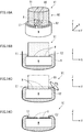
- Steps A1-A4 are performed sequentially, as shown in FIG. 7A to FIG. 7D .
- Steps B1 and B2 are carried out sequentially.
- Steps C1 and C2 are carried out sequentially, as shown in FIG. 9A and FIG. 9B .
- the electrodes E1 and E2 of the battery 5B are mounted on the front face 1a of the first rigid board 1, and also the booster circuit 5P, the oscillator 7O, and the modulator 7M are mounted on the back face 1b.
- This back face 1b is provided with the pads P1.
- a partition wall W between the electrodes E1 and E2 and an external wall WE surrounding the electrodes E1 and E2 are formed.
- a second sensor unit 52 except for the transmitting coil 7L are mounted.
- the power source capacitor 5C and the transmitter capacitor 7C are mounted on the front face 2a of the second rigid board 2, and the sensor 6 and the controller 8 are mounted on the back face 2b. This back face 2b is provided with the pads P2.
- the third rigid board 3 is disposed between the first rigid board 1 and the second rigid board 2 to stack these boards 1, 2, and 3. Specifically, into the above-described positioning holes H P1 , H P2 , and H P3 (indicated by a dashed line), a pin P (indicated by a dashed line) extending in the Z-axis direction is inserted to stack the rigid board 1, 2, and 3. Thus, the positioned rigid board 1, 2, and 3 of the respective positions in the XY plane are stacked.
- the pads P1, P2 and through-hole H T are electrically connected as shown in the FIG. 7D .
- the pads P1, P2, and through-hole H T are bonded by known materials such as anisotropic conductive films and solder.
- the sensor units 51 and 52 are electrically connected through through-hole H T .
- an adhesive may be poured between the first rigid board 1 and the third rigid board 3 and between the second rigid board 2 and the third rigid board 3 to increase the bonding strength between the boards.
- the base material part except for the rigid boards 1, 2, and 3 are removed for shaping.
- the pins P are removed from the positioning holes H P1 , H P2 , and H P3 described in the above stacking step, and the upper portion of the partition wall W at the rigid boards 1, 2, and 3 is rotated, being grasped by a clamp C, so that the base material part at a portion except for the rigid board 1, 2, and 3 is cut off by a trimming bit B.
- the base material part at a portion except for the rigid board 1, 2, and 3 may be cut off by moving the trimming bit B around the rigid boards 1, 2, and 3 while the upper portion of the partition wall W is grasped by the clamp C at the rigid boards 1, 2, and 3 without removing the pins P from positioning holes H P1 , H P2 , and H P3 described above in the above stacking step.
- the transmitting coil 7L is mounted on the front face 2a of the second rigid board 2. Specifically, the transmitting coil 7L is connected by melting the cream solder of front face 2a of the second rigid board 2.
- an internal module consisting of the rigid boards 1, 2, and 3 and the sensor unit 50 described above is immersed in the bioadaptable resin filled inside the capsule 9.
- the internal module is held at a position where the bioadaptable resin does not overcome the external wall WE so that the electrodes E1 and E2 are not immersed in the bioadaptable resin.
- the bioadaptable resin is cured.
- the process waits until the bioadaptable resin cures.
- a hole may be provided in rigid board 1 and 2, so that the punched portion 39 in the third rigid board 3 is easily filled with the bioadaptable resin.
- the outer shape is adjusted as shown in FIG. 9B . Specifically, the outer shape is adjusted by rounding the corners or cutting off the upper portion of the partition wall W grasped by the clamp C.
- the sensor device I of the present embodiment which is configured as described above, brings the following actions and effects.
- the sensor unit 50 are distributedly mounted on the board group 10 consisting only of the rigid boards 1, 2, and 3, and the sensor units 50 distributedly mounted are connected (electronically connected) through the through-holes H T on the third rigid board 3.
- the sensor device I uses a gastric acid battery as the battery 5B, the risk of liquid leakage and the restriction on the size of the sensor device due to a button battery can be eliminated as compared with a case where a button battery is used. Accordingly, such a battery can ensure the safety of the living body and contributes to the reduction in size of the sensor device I.
- the present second embodiment describes an example of a layout in which transmitting coil 7L' is embedded in the first rigid board 1'.
- the board in which transmitting coil 7L' is embedded is not limited to the first rigid board 1', and may alternatively be the second rigid board or the third rigid board that are not shown in the drawings, or may be all or some thereof.
- winding on front face 1a' and the winding on the back face 1b' are wound in patterns that do not overlap in a plan view.
- the first rigid board 1' of the sensor device II of the present embodiment has an outer diameter larger by the amount for embedding the transmitting coil 7L' therein.
- the winding of transmitting coil 7L' may make multiple turns in each layer, namely the front face 1a' and the back face 1b' (in the example of FIG. 11 , the winding makes two turns).
- the first rigid board 1' of the sensor device II' in this case can have a larger outer diameter in proportional to an increase of the number of turns on the same layer than the first rigid board 1' of the sensor device II shown in FIG. 10A and FIG. 10B .
- the sensor device II of the present embodiment which is configured as described above, can obtain the following actions and effects.
- the transmitting coil 7L' Since the transmitting coil 7L' is embedded in the first rigid board 1', the transmitting coil 7L' can be implemented as well as the first sensor unit 51'. In addition, the transmitting coil 7L' may be embedded when the first rigid board 1' is manufactured. This makes it possible to omit the steps such as post-implementation and external implementation of the transmitting coil 7L as performed in the first embodiment. Therefore, it is possible to reduce the manufacturing cost.
- the windings adjacent to each other along the Z-axis direction in the transmitting coil 7L' function as a capacitor.
- the capacitance of this capacitor is also referred to as "inter-pattern capacitance".
- the transmitting coil 7L' is unable to exert the function as an inductor, so that information is not transmitted to the outside.
- the third rigid board 3" of the sensor device III uses a multilayer board (having three or more layers of wiring layer) having a wiring layer in addition to the front face 3a" and the back face 3b".
- the wiring layers are exemplified by a first layer L1, a second layer L2, a third layer L3, a fourth layer L4, a fifth layer L5, and a sixth layer L6 that are aligned in this sequence in the Z direction.
- a six-layer board having these layers is an example of the third rigid board 3".
- the first layer L1 corresponds to the front face 3a" of the third rigid board 3
- the sixth layer L6 corresponds to the back face 3b" of the third rigid board 3".
- through-holes H L " as many (i.e., six) as the number of layers L1-L6 are provided to electrically connect each of the adjacent layers L1-L6 (in this example, a reference number is applied to the through-hole H L " electronically connected in each layer).
- These through-holes H L " are arranged in the different positions in the radius direction on the third rigid board 3" so that the respective windings of the layers L1-L6 are wound in the patterns not overlapping in a plane view or that the windings of the odd layers L1, L3, and L5 are wound in a pattern not overlapping with the pattern of the winding of the even layers L2, L4, and L6 in a plan view.
- the winding of the transmitting coil 7L" in the first layer L1 makes one turn as shown in FIG. 12A .
- the winding of transmitting coil 7L" makes one turn.
- the windings of two adjacent layers among these layers L1-L6 are connected via the holes H L ".
- the sensor device III of the present embodiment which is configured as described above, can obtain the following actions and effects
- the third rigid board 30 of a sensor device IV' may be composed of multiple standardized boards 30A and 30B.
- the sensor device IV of the present embodiment which is configured as described above, can obtain the following actions and effects.
- the sensor device III of the third embodiment and the sensor device IV of the present embodiment can eliminate the requirement for preparing each of the third rigid boards 3", 30A, and 30B.
- the boards 30A and 30B also as the third rigid board 3 it is possible to use common parts both in the sensor devices III and IV. This makes it possible to suppress manufacturing costs of the sensor devices III and IV different in type.
- the sensor device V of the fifth embodiment is different from the sensor device I of the first embodiment described above in the following points A-C.
- the sensor device V of the present embodiment which is configured as described above, brings the following actions and effects.
- the sensor device VI which is manufactured in this method has the same configuration as sensor device I of the first embodiment described above, but a masking member 80 is used in the manufacturing process. Therefore, in the description of the present embodiment, like reference numbers designate the same parts and elements as the sensor device I of the first embodiment, so repetitious description is omitted here.
- the method of manufacturing of the present embodiment is mainly different in postprocessing step from the method of manufacturing the sensor device I of the first embodiment described above.
- the method of manufacturing of the present embodiment is different from the first embodiment in that the structure corresponding to the external wall WE (see FIG. 3 ) formed in the first implementing step of the preprocessing step of the first embodiment is formed in the above Steps D2, D3, and D4 in the present embodiment.
- Steps D1, D2, D3, and D4 of the present embodiment forming of the partition wall W (see FIG. 3 ) is omitted.
- the exposed region R is masked using a masking member 80 shaped according to the exposed region R.
- the masking member 80 is set to have a dimension in the Z direction larger than that of the external wall WE described above in the first embodiment.
- This masking member 80 is formed of a soluble material having a property of dissolving by a solvent.
- the masking member 80 is exemplified by a cylindrical member.
- the masking member 80 is laminated and affixed to the exposed region R. In this way, the exposed region R is covered with and masked by a masking member 80 so that the exposed region R is not immersed in the bioadaptable resin.
- the internal module M consisting of the rigid boards 1, 2, and 3 and the sensor unit 50 (see FIG. 3 ) is sank and immersed in the bioadaptable resin filled inside the capsule 9. That is, internal module M is embedded in the bioadaptable resin. Then, the bioadaptable resin is cured. Alternatively, the process waits until the bioadatable resin cures.
- the allowable range of position in the Z direction for holding the internal module in this immersing and curing step is wider than the allowable range of the position in the Z direction for holding the internal module M in Step C1 described above.
- the outer shape is adjusted by rounding the corners of the overall portion and deleting a protruding portion 89 (indicated by a two-dot chain line) of the masking member 80. From this fact, it can be said that the shaping step is a shape adjusting step.
- the exposed region R is not yet exposed and still in a state of being masked.
- the masking is released by removing the masking member 80.
- the exposed region R which has been temporarily protected by the masking member 80 is exposed, and masking of exposed region R is released.
- a portion formed of the cured bioadaptable resin appears on the outer peripheral edge of the region where the masking member 80 was present and the portion serves as the configuration corresponding to the external wall WE of the sensor device I of the first embodiment.
- the method of manufacturing the sensor device VI of the present embodiment can obtain the following actions and effects.
- the allowable range of the position in the Z direction for holding the internal module M in this immersing and curing step can be enlarged with ease.
- the masking member 80 Since the masking member 80 is dissolved in a solvent in the releasing step, masking of exposed region R by the masking member 80 can be easily released.
- the immersing and curing step is satisfactorily carried out at least after the electrically connecting step and the masking step is satisfactorily carried out at least prior to the immersing and curing step.
- a masking step may be performed during the preprocessing step or the intermediate processing step.
- the immersing and curing step may be performed later than the masking step performed before the postprocessing step.
- the intermediate processing step can be omitted.
- modifications using a soluble masking member is exemplified by a first modification, a second modification, and a third modification.
- masking is achieved by covering the exposed region.
- a modification of masking by surrounding the periphery of the exposed region is exemplified by a fourth modification and a fifth modification.
- These modifications do not have to form the masking member of a soluble material, and do use a masking member formed of an insoluble material.
- the fourth and the fifth modifications do not require the releasing step of releasing the masking of the aforementioned Step D4.
- two masking members 81 and 82 are used. Specifically, the first masking member 81 corresponding to the electrode E1 and the second masking member 82 corresponding to the electrode E2 are used. These masking members 81 and 82 are spaced from each other with a space corresponding to partition wall W of the sensor device I of the first embodiment.
- a portion, serving as a configuration corresponding to partition wall W, can be formed of the cured bioadaptable resin between masking members 81 and 82.
- the second modification uses a masking member formed of the masking members 81 and 82 of the first modification connected to each other but spaced apart with a space corresponding to at least the partitioning wall W.
- this modification uses a portal-shaped masking member (i.e., columns tops of which are connected to each other) for the electrodes E1 and E2.
- the third modification uses a masking member formed of a soluble material that can be dissolved by a body fluid.
- the masking member dissolves when the sensor device is taken and comes into contacted with and immersed in a body fluids. Therefore, it is possible to omit the releasing step, which contributes to simplification of the producing step of the sensor device.
- the protruding part is removed in the shaping step in order to increase the safety.
- the fourth modification uses a masking member having a shape surrounding the exposed region (i.e., shape corresponding to the exposed region).
- a cylindrical member is exemplified as a masking member.
- this modification since the masking member does not cover the exposed region, so the releasing step of the masking member can be omitted.
- this embodiment which does not release the masking member, preferably forms the masking member with a bioadaptable resin.
- the masking member of the present modification is, in the masking step, laminated and affixed to the internal module in such an arrangement that the masking member forms a peripheral wall surrounding the exposed region.
- This masking member has a dimension in the Z direction set larger than the external wall WE (see FIG. 3 ) described above in the first embodiment.
- the outer shape is adjusted by rounding the corners of the overall portion and deleting a protruding portion of the masking member. After this shaping step, part of the masking member appears to serve as a configuration corresponding to the external wall WE.
- the masking member of the present modification which can mask the exposed region by surrounding the exposed region and therefore omit the releasing step, contributes to simplification of the method of manufacturing the sensor device.
- the above fourth modification which uses the cylindrical member as the masking member, can be applied to the configuration corresponding to the external wall WE (see FIG. 3 ), but is not applied to the configuration corresponding to the partition wall W (see FIG. 3 ).
- the fifth modification uses a masking member having shapes conform to the partition wall W as well as the external wall WE. Specifically, this modification uses a masking member in the cylindrical form of the fifth modification that additionally has a wall portion extending in the diametrical direction and also extending in the Z direction.
- the masking member of the present modification can form a structure corresponding to the partition wall W in addition to the operation and effects of the fifth modification.
- each of the rigid boards that constitute the board group is not limited to a layout in which a single rigid board is placed for a single base material.
- multiple rigid boards may be arranged for each of the base material 100, 200, and 300.
- the stacking step required for each sensor device can be carried out collectively as compared with a layout that arranges a single rigid board on a single base material.
- the position of the base materials 100, 200, and 300 can be determined simply by inserting the positioning pins PO into positioning holes H P100 , H P200 , and H P300 . Therefore, it is possible to manufacture multiple sensor devices at a time. Therefore, it is possible to further suppress the manufacturing cost.
- the board group may consist of at least two boards. That is, one board in which one part of a sensor unit is mounted and the other board in which the other part of the sensor unit is mounted may constitute the board group, and the one part and the other part of the sensor unit may be electrically connected in the stacking direction (the Z direction described above) of the board group.
- the coil (the other part) may be embedded in the other board, and other sensors (one part) may be embedded in the one board.
- the coil on the other board and the sensors the one part of the sensor unit on the one board are electrically connected by interposing a known material such as a anisotropic conductive film or an solder described above between the respective pads provided on the one and the other boards.
- this case may use a sensor device in which the second sensor unit 52 is mounted on the first rigid board 1 (one board) in addition to the first sensor unit 51, the second rigid board 2 is omitted, and the transmission coils 7' and 7" shown in FIGS. 10-13 are mounted on the third rigid board 3 (the another board) with respect to the sensor device I shown in FIG. 3 .
- the swallowing sensor device that has a structure in which the second rigid board is omitted; and the first rigid board (one board) on which one part of the sensor unit is mounted and the third rigid board (the other board) or the fourth board (the other board) on which the other part of the sensor unit is mounted are electrically connected in the stacking direction, it is possible to reduce the number of overall parts and therefore to reduce the size.
- the sensor device has a simple structure and obtains the above actions and effects.
- the transmitting coil is satisfactorily wound on at least one or more layers or two or more layers.
- a transmitting coil may be wound on at least one of front face and back face of each rigid board.
- the transmitting coil is wound on at least one of the front face, the back face, and the other inner layers.
- the sensor device is not limited to the application of being swallowed by the subject, but may alternatively applied to being circulated through the inside of the pipes of the plant or its mechanical equipment.
- the sensor device has possibility to be applied to various locations where detection has conventionally been difficult to be accomplished.
Landscapes
- Health & Medical Sciences (AREA)
- Life Sciences & Earth Sciences (AREA)
- Engineering & Computer Science (AREA)
- Physics & Mathematics (AREA)
- Animal Behavior & Ethology (AREA)
- Veterinary Medicine (AREA)
- Biophysics (AREA)
- Pathology (AREA)
- Public Health (AREA)
- Biomedical Technology (AREA)
- Heart & Thoracic Surgery (AREA)
- Medical Informatics (AREA)
- Molecular Biology (AREA)
- Surgery (AREA)
- General Health & Medical Sciences (AREA)
- Endocrinology (AREA)
- Gastroenterology & Hepatology (AREA)
- Physiology (AREA)
- Microelectronics & Electronic Packaging (AREA)
- Optics & Photonics (AREA)
- General Chemical & Material Sciences (AREA)
- Chemical Kinetics & Catalysis (AREA)
- Chemical & Material Sciences (AREA)
- Manufacturing & Machinery (AREA)
- Measurement Of The Respiration, Hearing Ability, Form, And Blood Characteristics Of Living Organisms (AREA)
- Combinations Of Printed Boards (AREA)
- Endoscopes (AREA)
- Measuring And Recording Apparatus For Diagnosis (AREA)
- Coils Or Transformers For Communication (AREA)
- Parts Printed On Printed Circuit Boards (AREA)
Abstract
Description
- The present invention relates to a swallowing sensor device preferably applied to use in detecting vital signs and a method of producing the same.
- Conventionally, a sensor device with a sensor unit incorporated in a capsule has been known. Such a swallowing sensor device of a capsule type is swallowed by a subject and used to detect vital signs in the internal body.
- The above sensor device incorporates therein sensor units exemplified by sensors such as a thermometer or a camera and additional devices relating to these sensors as well as a board in which the sensor units are mounted.
- Such a sensor device incorporating various devices requires a shape and a compact-size that can be easily swallowed. To satisfy the above requirement, it has been proposed that the devices to be incorporated are distributedly arranged in multiple boards, rather than arranged in a single board. Furthermore, it has also been proposed to connect sensor units mounted on multiple rigid boards by one or more flexible boards.
- For example, in a rigid-flexible board in which rigid boards provided with sensor units are connected by one or more flexible board, a sensor device in which the rigid boards are folded to be stacked by the flexible boards (see Patent Document 1).
- [Patent Document 1] Japanese Laid-open Patent Publication No.
2006-271520 - However, since a rigid-flexible board is generally more expensive than a rigid board, a sensor device using a rigid-flexible board as described above may increase the material cost. Further, since assembling of the sensor device requires bending by a flexible board, assembly cost may also rise. Not only to suppress the increase in costs caused by the use of such a flexible board, the swallowing sensor device is required to reduce the cost in the overall manufacturing process. Therefore, in order to suppress the manufacturing cost of the swallowing sensor device, there is room for improvement.
- With the foregoing problems in view, the object of the present invention is to suppress the manufacturing cost of a swallowing sensor device. In addition to this object, an effect which is derived from each configuration of an embodiment to carry out the invention to be described below and which conventional technique does not attain is as another object of the present disclosure.
-
- (1) The swallowing sensor device disclosed herein comprising: a sensor unit that includes a sensor and a device configured to wirelessly transmit information detected by the sensor; and a board group formed by stacking a plurality of rigid boards, wherein the board group includes a fist rigid board on which one part of the sensor unit is mounted; a second rigid board on which other part of the sensor unit except for the one part of the sensor unit is mounted; and a third rigid board being disposed between the first rigid board and the second rigid board and comprising a through-hole drilled thereon, the through-hole being configured to electrically connect the one part and the other part of the sensor unit.
- (2) The other swallowing sensor device disclosed herein comprising: a sensor unit that includes a sensor and a device configured to wirelessly transmit information detected by the sensor; and a board group formed by stacking a plurality of rigid boards, wherein the board group comprises one board on which one part of the sensor unit is mounted; another board on which other part of the sensor unit is mounted; and the one part mounted on the one board and the other part mounted on the another board are electrically connected in a direction of stacking the board group.
- (3) The method of manufacturing a swallowing sensor device, the method comprising: stacking and electrically connecting.
- In the stacking, stack a fist rigid board on which one part of a sensor unit comprising a sensor and a device configured to wirelessly transmit information detected by the sensor is mounted, a second rigid board on which other part of the sensor unit except for the one part of the sensor unit is mounted, and a third rigid board comprising a through-hole drilled thereon for electrically connecting the one part and the other part such that the third rigid board is arranged between the first rigid board and the second rigid board.
- In the electrically connecting, electrically connect the one part mounted on the first rigid board and the other part mounted on the second rigid board stacked in the stacking through the through-hole of the third rigid board.
- According to the present invention, it is possible to electrically connect sensor units distributedly arranged in the first rigid board and the second rigid board through the through-holes of the third rigid board. This makes it possible to manufacture a swallowing sensor device without using a flexible board. Consequently, it is possible to suppress the manufacturing cost of the swallowing sensor device.
-
-
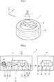
FIG. 1 is a perspective view showing an external appearance of a swallowing sensor device of a first embodiment; -
FIG. 2 is a schematic circuit diagram showing a sensor unit incorporated in a swallowing sensor device of the first embodiment; -
FIG. 3 is a schematic diagram illustrating a main part of a swallowing sensor device of the first embodiment; -
FIG. 4A and FIG. 4B are plan views showing a first rigid board used in a swallowing sensor device of the first embodiment,FIG. 4A showing a front face of the first rigid board, andFIG. 4B showing a back face of the first rigid board; -
FIG. 5A and FIG. 5B are plan views showing a second rigid board used in a swallowing sensor device of the first embodiment,FIG. 5A showing a front face of the second rigid board, andFIG. 5B showing a back face of the second rigid board; -
FIG. 6 is a plan view illustrating a third rigid board used in a swallowing sensor device of the first embodiment; -
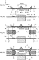
FIG. 7A, FIG. 7B, FIG. 7C, and FIG. 7D are diagrams showing a preprocessing step of a method of manufacturing a swallowing sensor device of the first embodiment,FIG. 7A showing a first implementing step,FIG. 7B showing a second implementing step,FIG. 7C showing a stacking step, andFIG. 7D showing an electrically connecting step; -
FIG. 8A and FIG. 8B are diagrams showing an intermediate processing step of a method of manufacturing a swallowing sensor device of the first embodiment,FIG. 8A showing a trimming step, andFIG. 8B showing a third implementing step; -
FIG. 9A and FIG. 9B are diagrams illustrating an postprocessing step of a method of manufacturing a swallowing sensor device of the first embodiment,FIG. 9A showing an immersing and curing step, andFIG. 9B showing a shaping step; -
FIG. 10A and FIG. 10B are plan views showing a first rigid board used in a swallowing sensor device of a second embodiment,FIG. 10A showing a front face of the first rigid board, andFIG. 10B showing a back face of the first rigid board; -
FIG. 11A and FIG. 11B are plan views showing a first rigid board used in a swallowing sensor device of a modification of the second embodiment,FIG.11A showing a front face of the first rigid board, andFIG. 11B showing a back face of the first rigid board; -
FIG. 12A, FIG. 12B, FIG. 12C, FIG. 12D, FIG. 12E, and FIG. 12F are plan views showing a third rigid board used in a swallowing sensor device of a third embodiment,FIG. 12A showing a first layer (front face) of the third rigid board,FIG. 12B showing a second layer of the third rigid board,FIG. 12C showing a third layer of the third rigid board,FIG. 12D showing a fourth layer of the third rigid board,FIG. 12E showing a fifth layer of the third rigid board, andFIG. 12F showing a sixth layer (back face) of the first rigid board; -
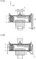
FIG. 13 is a schematic diagram illustrating a main part of a swallowing sensor device of a fourth embodiment; -
FIG. 14 is a schematic diagram illustrating a main part of a swallowing sensor device of a modification to the fourth embodiment; -
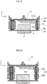
FIG. 15 is a schematic diagram illustrating a main part of a swallowing sensor device of a fifth embodiment; -
FIG. 16A, FIG. 16B, FIG. 16C and FIG. 16D are diagrams illustrating a postprocessing step of a method of manufacturing a swallowing sensor device of the sixth embodiment,FIG. 16A showing a masking step,FIG. 16B showing a immersing and curing step,FIG. 16C showing a shaping step, andFIG. 16D showing a releasing step; and -
FIG. 17 is a perspective view illustrating an exemplary process of manufacturing a swallowing sensor device. - Hereinafter, description will now be made in relation to an embodiment for carrying out a swallowing sensor device (hereinafter abbreviated as a "sensor device").
- The sensor device of the present embodiment is formed by incorporating boards being stacked on which sensor units are mounted.
- Here, a sensor device which is swallowed and used by a subject is exemplified. An example to the target to be detected by the sensor device is the vital sign of the subject. An example of the vital signs is the internal temperature (hereinafter referred to as "deep body temperature") of the subject at rest.
- In the drawings to be referenced in the following description, the positive-oriented orthogonal coordinate system having the X axis, the Y axis, and Z axis is defined as the reference of the orientation, and the sensor device shall be in a predetermined orientation. The sensor device in a predetermined orientation is assumed that the boards extend along both the X-axis and Y-axis, and the stacking direction of the boards is along the Z direction.
- Incidentally, illustration of connection lines between devices in a plan view and the perspective views is omitted, for convenience. Further, in the cross-sectional views and the schematic views, the thicknesses of sensor units are exaggerated and some devices which are not arranged on the same cross-section but are arranged on the same plane appear.
- Hereinafter, sensor devices according to a first embodiment, a second embodiment, a third embodiment, a fourth embodiment, and a fifth embodiment will be sequentially detailed. The embodiments to be detailed merely illustrative and are not intended to exclude the application of various modifications and techniques not explicitly described in the embodiment.
- First, referring to
FIGS. 1 and3 , an overview of a sensor device I will now be described. - The sensor device I is provided with a
capsule 9 that incorporates therein aboard group 10 and asensor unit 50. Thecapsule 9 forms the outer shell of the sensor device I. Thiscapsule 9 is made of material which is hardly dissolved by digestive juice such as the gastric juice and the intestinal juice. - The sensor device I is formed into a shape easy to swallow. Here, a sensor device I having an approximate shape in which the upper and lower bottoms of the cylinder bulge. However, various shapes, such as truncated, spherical, and disk-shaped, may be applied to the sensor device I. Incidentally, the sensor device I illustrated here is almost covered by the
capsule 9, but part of thesensor unit 50 are exposed. - Hereinafter, the basic circuit configuration of the sensor device I will be described, followed by a detailed description of the specific layout configuration.
- As shown in
FIG. 2 , thesensor unit 50 incorporated in sensor device I constitutes a circuit (hereinafter abbreviated as "transmitter circuit") 5T for transmitting the detected information to the outside. - The
transmitter circuit 5T is provided with asensor 6 that detects the temperature, and adevice 60 that wirelessly transmits information detected by thesensor 6. Thedevice 60 includes atransmitter 7 that transmits (outputs) information to the outside, apower source unit 5 that supplies electric power, and acontroller 8 that controls, for example, thesensor 6 andtransmitter 7. - In addition, information transmitted from sensor device I are received by a
receiver circuit 5R provided outside the body of the subject who swallowed the sensor device I. - The
receiver circuit 5R is provided with a coil (hereinafter abbreviated as "receiving coil") 5L for receiving information transmitted from the sensor device I, ademodulator 5D, and a power source unit 5S that supplies electric power todemodulator 5D. Thisreceiver circuit 5R is also provided with adisplay 5E that displays the received information. - The
power source unit 5 is provided with abattery 5B, which is a supplying source of electric power. In addition to thebattery 5B, thepower source unit 5 also includes abooster circuit 5P that boosts the voltage of thebattery 5B and supplies the boosted voltage, and an electricpower source capacitor 5C. - Here, a gastric acid battery, which generates electric power between two electrodes E1 and E2 when being brought into contact with gastric acid (an acidic fluid) as a
battery 5B. Alternatively, abattery 5B may be used which generates electric power between the two electrodes E1 and E2 when being brought into contact with another body fluid, such as intestinal fluid as well as gastric acid. - For the electrodes E1 and E2, a magnesium (Mg) thin film is used for one electrode, i.e., the negative electrode E1 (first electrode) and a gold (Au) thin film is used for the other electrode, i.e., the positive electrode E2 (second electrode).
- As an alternative to the above gastric acid battery, various power supplying source such as a module that wirelessly supplies electric power or a button battery may be used as the
battery 5B. - The electrodes E1 and E2 are connected to the following
booster circuit 5P. - The
booster circuit 5P is a functional circuit that boosts the input voltage between the electrodes E1, E2, and outputs the boosted voltage. For example, thebooster circuit 5P, when a voltage of about 1.0 [V] is input from the electrodes E1 and E2, outputs a voltage of about 3.0 [V]. - An power source capacitor 5C to be described next is connected to the output side of this
booster circuit 5P. - The
power source capacitor 5C exerts a function of smoothing the current or voltage. In addition, the power source capacitor 5C also exerts a function of retaining charged charges like a storage battery. Here, as thepower source capacitor 5C, a Multi-Layer Ceramic Capacitor (MLCC) having an electric capacitance of 220 [µF] is used. - The
sensor 6, thetransmitter 7, and thecontroller 8 are connected in parallel to the abovepower source capacitor 5C, and power is supplied to each of thesensor 6, thetransmitter 7, and thecontroller 8. - The
sensor 6 is a temperature sensor that detects the temperature. That is, thesensor 6 constitutes a part (temperature measuring unit) that measures the temperature in the sensor device I. Here, among the general-purpose digital-temperature sensors, one small in size and low in power consumption is used as thesensor 6. - The information detected in this
sensor 6 is input into thecontroller 8. - The
transmitter 7 is provided with an oscillator 7O that generates a carrier wave, amodulator 7M that outputs a modulated wave obtained by modifying the carrier wave generated by the oscillator 7O and superimposing information detected by thesensor 6 on the modified carrier wave, and aresonant circuit 7R that outputs the modulated wave from the modulator 7M to the outside. Here, theresonant circuit 7R in which thetransmitter capacitor 7C and the transmittingcoil 7L (coil) are connected is used. - That is, the carrier wave from the oscillator 7O is modulated by the
modulator 7M to generate a modulated wave containing a signal of the detected temperature obtained by thesensor 6. This modulated wave is outputted in the form of an electromagnetic wave from theresonant circuit 7R. - The above-described electromagnetic wave communication requires both the transmissiveness through the living body such as the digestive tract and the other body of the subject that swallowed the sensor device I and the energy-loss suppression. Generally, electromagnetic wave has a first characteristic that the bioabsorption loss increases in the frequency region higher than 100 [MHz], and a second characteristic that, when the transmitting
coil 7L is small in size, the transmission efficiency lowers as the frequency is lower. Therefore, the frequency of the electromagnetic wave to be output is preferably selected, considering the first characteristic and the second characteristic described above. - Here, a carrier wave of 13.56 [MHz] is employed. Manchester coding is also used as the coding scheme, and the binary phase shift keying (BPSK) is used as the modulation scheme.
- According to the above setting, a single transmission requires the time of about 1 [ms] and the power consumption of about 3 [pJ].
- The
controller 8 is connected to thesensor 6 and themodulator 7M. Thiscontroller 8 carries out the various controls 1-3 listed below. - Control 1: detection by the
sensor 6 - Control 2: encapsulation of information detected by the
sensor 6 - Control 3: setting the outputting frequency from the
resonant circuit 7R -
Control 1 is an actuation control that activates thesensor 6 to detect the temperature. -
Control 2 is a signal control that generates information to be superimposed on the carrier wave through encapsulation of information. -
Control 3 is an actuation control that resonates, via themodulator 7M, theresonant circuit 7R. - In addition to the above, the
controller 8 may be connected to the oscillator 7O. Further, thecontroller 8 may be involved in power source control that switches the ON/OFF of power source of at least one of thesensor 6, the oscillator 7O, and themodulator 7M. - In the
receiver circuit 5R, the electromagnetic wave from thetransmitter circuit 5T described above is received at the receivingcoil 5L. The electromagnetic wave received at the receivingcoil 5L is demodulated by thedemodulator 5D so that information (i.e., information of "deep body temperature") detected by thesensor 6 is extracted. The receivingcoil 5L and thedemodulator 5D are supplied with the electric power from the power source unit 5S. In thisreceiver circuit 5R, the information of the deep body temperature extracted by thedemodulator 5D is displayed on thedisplay 5E, and the electric power from the power source unit 5S is also supplied to thedisplay 5E. - Incidentally, the information of the deep body temperature extracted by the
demodulator 5D is not limited to being displayed on thedisplay 5E and may alternatively be stored into an on-line storage through a non-illustrated communication network. In this case, the on-line storage can be configured such that the data therein can be browsed from electronic devices, such as a smartphone or a notebook computer, that can be connected to the above communication network. - Furthermore, suggestions and warnings regarding health conditions can also be informed the subject and the person concerned based on a database of vital signs containing information on the deep body temperature accumulated in the on-line storage. In addition, the sensor device I can be controlled according to the demands from the electronic equipment of the subject and the person concerned. Thus, it is also possible to use the sensor device I by utilizing the so-called big data or IoT (Internet of Things).
- Next, the layout configuration of the sensor device I will now be described in detail with reference to
FIGS. 3-6 . - As shown in
FIG. 3 , in the sensor device I, in addition to thesensor unit 50 constituting thetransmitter circuit 5T described above, aboard group 10 in whichsensor unit 50 are distributedly arranged is incorporated in thecapsule 9. In the sensor device I, the part inside thecapsule 9 except for thesensor unit 50 and theboard group 10 is filled with resin (indicated by halftone dots) As this resin, resin adaptable to a living body (hereinafter, referred to as "bioadaptable resin")is applied. - The
board group 10 consists of threerigid boards rigid boards rigid board 1 disposed on the upper side inFIG. 3 , a secondrigid board 2 disposed on the lower side inFIG. 3 , and a thirdrigid board 3 disposed between therigid boards - Further, these
rigid board rigid board 1, the top face inFIG. 3 is defined as a "front face 1a (first face)" and the lower face is defined as a "back face 1b (second face)". Similarly, in regard of the thirdrigid board 3, the top face inFIG. 3 is defined as a "front face 3a (first face)" and the lower face is defined as a "back face 3b (second face)". In contrast, in regard of the secondrigid board 2, the lower face inFIG. 3 is defined as "front face 2a (first face)" and top face is defined as "backface 2b (second face)". - As shown in
FIGS. 4-6 , each of therigid boards FIGS. 4 to 6 , the portions to be discarded are indicated by halftone dots). - The frames F1, F2, and F3 are the base material of the
rigid boards rigid boards - Incidentally, the shape of
rigid boards - Further, on portions of the frames F1, F2, and F3 that are to be discarded apart from the prospective
rigid boards rigid boards - These positioning holes HP1, HP2, and HP3 are arranged at positions that coincide with one another in a plan view when the
rigid boards - Therefore, by just stacking
rigid board FIG. 7 ), it is possible to determine the positions of therigid boards - On the present embodiment, one part (hereinafter referred to as "first sensor unit") 51 of the
sensor unit 50 is disposed on the firstrigid board 1. On the secondrigid board 2, the other part (hereinafter referred to as "second sensor unit") 52 excluding thefirst sensor unit 51 from thesensor unit 50 is disposed. In this example, nosensor unit 50 is disposed on the thirdrigid board 3. - Hereinafter, each of
rigid board - As shown in
FIG. 4A , thefront face 1a of the firstrigid board 1 is mounted with the negative electrode E1 and the positive electrode E2 of thebattery 5B. - These electrodes E1 and E2 are, as shown in
FIG. 3 , arranged such that the top faces thereof are exposed to the outside and are to be immersed directly in the gastric juice. Incidentally, the electrodes E1 and E2 are aligned along the Y direction as shown inFIG. 4A , but, for convenience of illustration, appear to align along the X direction inFIG. 3 . - Here, a partition wall W is extended between the electrodes E1 and E2. This partition wall W prevents the subject's stomach wall (the inner wall of the digestive system) from contacting both the electrodes E1 and E2, and prevents thermal injury (so-called burns) of the stomach wall due to a possible short circuit of the electrodes E1 and E2.
- Incidentally, the electrodes E1 and E2 are formed by a sputtering method on the
front face 1a of the firstrigid board 1 manufactured by a microfabrication technique (MEMS (Micro Electro Mechanical Systems) technique). - The
back face 1b of the firstrigid board 1 ofFIG. 4B is implemented with thebooster circuit 5P, the oscillator 7O and themodulator 7M. - The
above battery 5B, thebooster circuit 5P, the oscillator 7O, and themodulator 7M serve as thefirst sensor unit 51. - Furthermore, the
back face 1b of the firstrigid board 1 is provided with multiple pads P1 (also referred to as "lands", only one of which is indicated by a reference symbol), for connection (electrical connection) with thesecond sensor unit 52 mounted on the secondrigid board 2. Furthermore, themodulator 7M is connected to any one of the pads P1. - As shown in
FIG. 5A , thefront face 2a of the secondrigid board 2 is mounted with thepower source capacitor 5C and is further provided with the connecting terminal 70L and thetransmitter capacitor 7C of the transmittingcoil 7L (seeFIG. 3 ). The positions at which the transmittingcoil 7L and thetransmitter capacitor 7C are arranged are not limited to thefront face 2a of the secondrigid board 2, and may alternatively be thefront face 1a or theback face 1b of the firstrigid board 1, or theback face 2b of the secondrigid board 2. As shown inFIG. 5B , backface 2b of the secondrigid board 2 is mounted with thesensor 6 and thecontroller 8. Further, as shown inFIG. 3 , the transmittingcoil 7L is attached to thefront face 2a of the secondrigid board 2 on which thesecond sensor unit 52 is already implemented and is externally attached to theboard group 10. For example, the transmittingcoil 7L is connected to thefront face 2a of the secondrigid board 2 with solder paste. - The above
power source capacitor 5C, thesensor 6, thecontroller 8, the transmittingcoil 7L, andtransmitter capacitor 7C serves as thesecond sensor unit 52. - Furthermore, as shown in
FIG. 5B , theback face 2b of the secondrigid board 2 is provided with pads P2 (one of which is indicated by a reference symbol) at positions coincide with the pad P1 on theback face 1b of the firstrigid board 1 in a plan view. Further, the signal of the modulated wave outputted from the modulator 7M of the firstrigid board 1 is output to thetransmitter capacitor 7C through a connecting terminal 70L of the transmittingcoil 7L connected to the pad P2 corresponding to the pad P1 to which themodulator 7M is connected. - As shown in
FIG. 6 , on the thirdrigid board 3, through-holes HT (one of which is indicated by a reference symbol) are drilled for electric connection between thefirst sensor unit 51 and thesecond sensor unit 52. Incidentally, thefront face 3a and theback face 3b of the thirdrigid board 3 are configured the same as each other. - The through-holes HT are arranged at positions corresponding to the above-mentioned pads P1 and P2 in a plan view. The inner faces of these through-holes HT formed by drilling the third
rigid board 3 are plated with conductor such as solder or copper. The conductor of the through-hole HT is electrically connected to the above pads P1, P2 with known materials such as Anisotropic Conductive Films (ACFs) having conductivity in the Z direction or solder. - Alternatively, the pads P1 on the
back face 1b of the firstrigid board 1 and the pads P2 on theback face 2b of the secondrigid board 2 may be provided at offset positions in a plan view and may be electrically connected via wiring by the thirdrigid board 3. - In order to avoid interfering with the
booster circuit 5P, the oscillator 7O, themodulator 7M, thesensor 6, and thecontroller 8 mounted on the back faces 1b and 2b of the otherrigid boards rigid board 3 is provided with a portion (hereinafter referred to as "punched portion") 39 removed by punching. That is, the thirdrigid board 3 is formed into an annular shape. The multiple through-holes HT exemplarily illustrated inFIG. 6 are arranged on one side and the other side interposed by the punchedportion 39. Alternatively, multiple through-holes HT may be arranged around the punchedportion 39. - Next, a method of manufacturing the above sensor device I will now be described.
- In the method of manufacturing exemplified here, three steps of a preprocessing step A, an intermediate processing step B, a postprocessing step C are carried out in this sequence.
- In the preprocessing step A, the following Steps A1-A4 are performed sequentially, as shown in
FIG. 7A to FIG. 7D . - Step A1: a first implementing step of mounting the
first sensor unit 51 on the firstrigid board 1 - Step A2: a second implementing step of mounting the
second sensor unit 52 on the secondrigid board 2 - Step A3: a stacking step of stacking the
rigid boards - Step A4: electrically connecting step of electrically connecting the
sensor units - As shown in
FIG. 8A and FIG. 8B , in the intermediate processing step B, following Steps B1 and B2 are carried out sequentially. - Step B1: a trimming step of shaping the
rigid boards - Step B2: a third implementing step of completing an internal module by externally attaching the transmitting
coil 7L - In the postprocessing step C, the following Steps C1 and C2 are carried out sequentially, as shown in
FIG. 9A and FIG. 9B . - Step C1: an immersing and curing step of curing an internal module by immersing the module in resin
- Step C2: a shaping step of adjusting the outer shape
- In the first implementing step of Step A1, as shown in
FIG. 7A , the electrodes E1 and E2 of thebattery 5B are mounted on thefront face 1a of the firstrigid board 1, and also thebooster circuit 5P, the oscillator 7O, and themodulator 7M are mounted on theback face 1b. Thisback face 1b is provided with the pads P1. Furthermore, with respect tofront face 1a, a partition wall W between the electrodes E1 and E2 and an external wall WE surrounding the electrodes E1 and E2 are formed. - In the second implementing step of Step A2, as shown in
FIG. 7B , asecond sensor unit 52 except for the transmittingcoil 7L are mounted. Specifically, thepower source capacitor 5C and thetransmitter capacitor 7C are mounted on thefront face 2a of the secondrigid board 2, and thesensor 6 and thecontroller 8 are mounted on theback face 2b. Thisback face 2b is provided with the pads P2. - In the stacking step of Step A3, as shown in
FIG. 7C , the thirdrigid board 3 is disposed between the firstrigid board 1 and the secondrigid board 2 to stack theseboards rigid board rigid board - In the electrically connecting step of Step A4, the pads P1, P2 and through-hole HT are electrically connected as shown in the
FIG. 7D . Specifically, the pads P1, P2, and through-hole HT are bonded by known materials such as anisotropic conductive films and solder. Thus, thesensor units rigid board 1 and the thirdrigid board 3 and between the secondrigid board 2 and the thirdrigid board 3 to increase the bonding strength between the boards. - In the trimming step of Step B1, as shown in
FIG. 8A , the base material part except for therigid boards rigid boards rigid board rigid board rigid boards rigid boards - In the third implementing step of Step B2, as shown in
FIG. 8B , the transmittingcoil 7L is mounted on thefront face 2a of the secondrigid board 2. Specifically, the transmittingcoil 7L is connected by melting the cream solder offront face 2a of the secondrigid board 2. - In the immersing and curing step of Step C1, as shown in
FIG. 9A , an internal module consisting of therigid boards sensor unit 50 described above is immersed in the bioadaptable resin filled inside thecapsule 9. At this time, the internal module is held at a position where the bioadaptable resin does not overcome the external wall WE so that the electrodes E1 and E2 are not immersed in the bioadaptable resin. Then, the bioadaptable resin is cured. Alternatively, the process waits until the bioadaptable resin cures. A hole may be provided inrigid board portion 39 in the thirdrigid board 3 is easily filled with the bioadaptable resin. - In the shaping step of the Step C2, the outer shape is adjusted as shown in
FIG. 9B . Specifically, the outer shape is adjusted by rounding the corners or cutting off the upper portion of the partition wall W grasped by the clamp C. - The sensor device I of the present embodiment, which is configured as described above, brings the following actions and effects.
In the sensor device I, thesensor unit 50 are distributedly mounted on theboard group 10 consisting only of therigid boards sensor units 50 distributedly mounted are connected (electronically connected) through the through-holes HT on the thirdrigid board 3. - Therefore, it is possible to manufacture a sensor device I without using a flexible board. This makes it possible to suppress the cost of the board material. Further, it is possible to suppress the assembly cost by omitting the bending step with the flexible board. Consequently, it is possible to suppress the manufacturing cost of the sensor device I.
- In addition, since the sensor device I uses a gastric acid battery as the
battery 5B, the risk of liquid leakage and the restriction on the size of the sensor device due to a button battery can be eliminated as compared with a case where a button battery is used. Accordingly, such a battery can ensure the safety of the living body and contributes to the reduction in size of the sensor device I. - Next, description will now be made in relation to a sensor device II of the second embodiment with reference to
FIGS. 10A and FIG. 10B . - The sensor device II of the second embodiment is different from that of the first embodiment in that the transmitting
coil 7L' is embedded in board group 10' whereas the transmittingcoil 7L is externally attached to theboard group 10 in the sensor device I of the first embodiment described above. In contrast to the sensor device I of the first embodiment described above, which mounts thetransmitter capacitor 7C on thefront face 2a of the secondrigid board 2, the present embodiment is different in that thetransmitter capacitor 7C' of the present embodiment is mounted on theback face 1b' of the first rigid board 1'. The remaining configurations are the same as the first embodiment, so like reference numbers designate the same elements and parts, and redundant description is omitted here. - The present second embodiment describes an example of a layout in which transmitting
coil 7L' is embedded in the first rigid board 1'. However, the board in which transmittingcoil 7L' is embedded is not limited to the first rigid board 1', and may alternatively be the second rigid board or the third rigid board that are not shown in the drawings, or may be all or some thereof. - Around the outer periphery of the first rigid board 1' of the sensor device II, a winding of the transmitting
coil 7L' is embedded. - On this first rigid board 1', through-holes HL' (different from the through-holes HT described above) that electrically connect the
front face 1a' to theback face 1b' are drilled at points different from the first sensor unit 51' and the pads P1 in a plan view. Then, the winding of transmittingcoil 7L' in the first rigid board 1' makes one turn in thefront face 1a' as shown inFIG. 10A and another winding makes another turn in theback face 1b' as shown inFIG. 10B , and the windings on thefront face 1a' and theback face 1b' are connected through the through-holes HL'. - In addition, the winding on
front face 1a' and the winding on theback face 1b' are wound in patterns that do not overlap in a plan view. - Incidentally, as compared with the first
rigid board 1 in sensor device I of the first embodiment, the first rigid board 1' of the sensor device II of the present embodiment has an outer diameter larger by the amount for embedding the transmittingcoil 7L' therein. - Alternatively, as shown in
FIGS. 11A and 11B , the winding of transmittingcoil 7L' may make multiple turns in each layer, namely thefront face 1a' and theback face 1b' (in the example ofFIG. 11 , the winding makes two turns). The first rigid board 1' of the sensor device II' in this case can have a larger outer diameter in proportional to an increase of the number of turns on the same layer than the first rigid board 1' of the sensor device II shown inFIG. 10A and FIG. 10B . - The sensor device II of the present embodiment, which is configured as described above, can obtain the following actions and effects.
- Since the transmitting
coil 7L' is embedded in the first rigid board 1', the transmittingcoil 7L' can be implemented as well as the first sensor unit 51'. In addition, the transmittingcoil 7L' may be embedded when the first rigid board 1' is manufactured. This makes it possible to omit the steps such as post-implementation and external implementation of the transmittingcoil 7L as performed in the first embodiment. Therefore, it is possible to reduce the manufacturing cost. - Here, the windings adjacent to each other along the Z-axis direction in the transmitting
coil 7L' function as a capacitor. The capacitance of this capacitor is also referred to as "inter-pattern capacitance". In the region of the higher frequency than the predetermined resonant frequency where the inter-pattern capacity becomes dominant over the inductance of the transmittingcoil 7L', the transmittingcoil 7L' is unable to exert the function as an inductor, so that information is not transmitted to the outside. - In contrast, since the windings of transmitting
coil 7L' are wound in respective patterns that do not overlap in a plan view, it is possible to suppress the inter-pattern capacitance, so that the setting region of the resonant frequency can be secured. For example, a higher resonant frequency than that in the sensor device I of the first embodiment can be set. - In addition, a layout in which the windings of the transmitting
coil 7L' makes multiple turns in each layer of thefront face 1a' and theback face 1b' can ensure the inductance of the embedded transmittingcoil 7L'. - Next, with reference to
FIGS. 12A to 12F , a sensor device III of the third embodiment will now be described. - The sensor device III of the third embodiment is different from that of the second embodiment in that the windings of transmitting
coil 7L" are arranged in three or more layers whereas the windings of transmittingcoil 7L' are arranged in two layers, i.e., thefront face 1a' and theback face 1b' in the sensor device II of the second embodiment described above. The remaining configuration is the same as the second embodiment, so repetitious description is omitted here. - In the present embodiment, a layout that embeds the transmitting
coil 7L" in the thirdrigid board 3" is exemplified. However, the board in which the transmittingcoil 7L" is embedded is not limited to the thirdrigid board 3", and may alternatively be the first rigid board or the second rigid board not shown. - The third
rigid board 3" of the sensor device III uses a multilayer board (having three or more layers of wiring layer) having a wiring layer in addition to thefront face 3a" and theback face 3b". Here, the wiring layers are exemplified by a first layer L1, a second layer L2, a third layer L3, a fourth layer L4, a fifth layer L5, and a sixth layer L6 that are aligned in this sequence in the Z direction. A six-layer board having these layers is an example of the thirdrigid board 3". Incidentally, the first layer L1 corresponds to thefront face 3a" of the thirdrigid board 3", and the sixth layer L6 corresponds to theback face 3b" of the thirdrigid board 3". - In the third
rigid board 3", the winding of the transmittingcoil 7L" is embedded in each of the first layer L1, the second layer L2, the third layer L3, the fourth layer L4, the fifth layer L5, and the sixth layer L6. - On this third
rigid board 3", through-holes HL" (different from the through-holes HT described above) that electrically connects thefront face 3a" to theback face 3b" are drilled at points different from the through-holes HT" in a plan view. - Further, through-holes HL" as many (i.e., six) as the number of layers L1-L6 are provided to electrically connect each of the adjacent layers L1-L6 (in this example, a reference number is applied to the through-hole HL" electronically connected in each layer). These through-holes HL" are arranged in the different positions in the radius direction on the third
rigid board 3" so that the respective windings of the layers L1-L6 are wound in the patterns not overlapping in a plane view or that the windings of the odd layers L1, L3, and L5 are wound in a pattern not overlapping with the pattern of the winding of the even layers L2, L4, and L6 in a plan view. - Incidentally, parts that connect layers of the first layer L1, the second layer L2, the third layer L3, the fourth layer L4, the fifth layer L5, and the sixth layer L6 that are provided to the third
rigid board 3" are not limited to the through-hole HL" but alternatively may be non-through-holes, such as IVHs (Inner Via Holes) or BVHs (Blind Via Holes) . - As shown in
FIG. 12A , the winding of the transmittingcoil 7L" in the first layer L1 makes one turn as shown inFIG. 12A . Similarly, in each of the second layer L2 shown inFIG. 12B , the third layer L3 shown inFIG. 12C , the fourth layer L4 shown inFIG. 12D , the fifth layer L5 shown inFIG. 12E , and the sixth layer L6 shown inFIG. 12F , the winding of transmittingcoil 7L" makes one turn. The windings of two adjacent layers among these layers L1-L6 are connected via the holes HL". - The sensor device III of the present embodiment, which is configured as described above, can obtain the following actions and effects
- Since the windings of the transmitting
coil 7L" are wound around the respective layers of the thirdrigid board 3" in the form of the multilayer board, it is possible to ensure the inductance of the embedded transmittingcoil 7L". - In addition, since the windings of the respective layers L1-L6 are arranged so as not to overlap each other in a plan view by multiple through-holes HL" having different radial positions, it is also possible to suppress the inter-pattern capacitance while securing the inductance, so that the setting region of the resonant frequency can be secured.
- Next, description will now be made in relation to a sensor device IV of the fourth embodiment with reference to
FIG. 13 . - The sensor device IV of the fourth embodiment is different from the sensor device I of the first embodiment described above in the following
points - Difference 1: a layout in which the front and back sides of the second
rigid board 2 of the first embodiment are inverted - Difference 2: using a third
rigid board 30 having a dimension in the Z direction larger than that of the thirdrigid board 3 of the first embodiment - The configuration except for the third
rigid board 30 is the same as the first embodiment, so repetitious description is omitted here. - In regard to the above
different point 1, thepower source capacitor 50C of the present embodiment has a similar holding amount of charged charge to that of thepower source capacitor 5C of the first embodiment, but has larger dimension in the Z direction than those of thesensor 6, the oscillator 7O, and thecontroller 8. With this structure, in cases where a thin thirdrigid board 3 as used in the first embodiment is used, thepower source capacitor 50C mounted onback face 20b of the secondrigid board 20 may interfere with theback face 100b or thefirst sensor unit 51 of the firstrigid board 100 as described in theabove Difference 1. - As a solution to the above, this embodiment uses a third
rigid board 30 thicker than that of the thirdrigid board 3 of the first embodiment as described inDifference 2. - For this third
rigid board 30, a multilayer board is used as in the third embodiment, the windings of the transmitting coil (not shown) are wound around the respective layers. Generally, the number of layers of a multilayer board is set larger as the thickness of board increases. The thirdrigid board 30 according to such a layer number setting is used. That is, although the thirdrigid board 30 in which more layers than the thirdrigid board 3" of the third embodiment are set is incorporated in the sensor device IV, the entire dimension in the Z direction of the sensor device I and that of the sensor device IV are not different. Further, apower source capacitor 50C having a larger holding amount of charged charge than that of thepower source capacitor 5C of the first embodiment may be used. - In addition, as shown in
FIG. 14 , the thirdrigid board 30 of a sensor device IV' may be composed of multiplestandardized boards - For example, a standardized board may be used as the third
rigid board 3" in the sensor device III of the third embodiment, and theboards rigid board 30 of the present embodiment. - The sensor device IV of the present embodiment, which is configured as described above, can obtain the following actions and effects.
- Since the winding of the transmitting coil is wound around each layer of the third
rigid board 30 in which more layers than those of the thirdrigid board 3" of the third embodiment are set without changing the overall dimension of the Z direction of the sensor device IV from the sensor device I, it is possible to increase the inductance. Further, in cases where thepower source capacitor 50C having a larger holding amount of charged charge than that of thepower source capacitor 5C of the first embodiment is used, it is possible to increase the detection frequency or the number of times of detection by the sensor device IV, which can increase the output frequency or the number of times of output of the detected information. - In addition, in cases where the third
rigid board 30 consists of multiplestandardized boards rigid boards 3", 30A, and 30B. Thus, by using theboards rigid board 3", it is possible to use common parts both in the sensor devices III and IV. This makes it possible to suppress manufacturing costs of the sensor devices III and IV different in type. - Next, description will now be made in relation to a sensor device V of the fifth embodiment with reference to
FIG. 15 . - The sensor device V of the fifth embodiment is different from the sensor device I of the first embodiment described above in the following points A-C.
- Difference A: using the third
rigid board 3" the same as that in the third embodiment in place of the thirdrigid board 3 - Difference B: a fourth
rigid board 40 which is added on the opposite side to the thirdrigid board 3" with respect to the second rigid board - Difference C: using the
power source capacitor 50C the same as the fourth embodiment used in place of thepower source capacitor 5C - Furthermore, likewise the third
rigid board 3", a multi-layer board is used as the fourthrigid board 40, and the windings of transmitting coil not shown are wound in each layer. Such windings are connected to transmitting coil embedded in the thirdrigid board 3". This means that the transmitting coil is embedded distributedly in the thirdrigid board 3" and the fourthrigid board 40. - Moreover, the third
rigid board 3" and the fourthrigid board 40 are the same standard products. That is, thestandardized boards 3", 40 are used in the sensor device V. The remaining configurations are the same as the first and the third embodiments, so redundant description is omitted here. - The sensor device V of the present embodiment, which is configured as described above, brings the following actions and effects.
- Since the transmitting coil is embedded in the fourth
rigid board 40 in addition to the thirdrigid board 3", it is possible to increase the inductance as compared with sensor device III of the third embodiment. - In addition, since the
standardized boards 3" and 40 are used, it is possible to use common parts both in the sensor devices III and V. This makes it possible to suppress manufacturing costs of the sensor devices III and V different in type. - Next, description will now be made in relation to a method of manufacturing a sensor device VI according to a sixth embodiment with reference to
FIG. 16A to FIG. 16D . - The sensor device VI, which is manufactured in this method has the same configuration as sensor device I of the first embodiment described above, but a masking
member 80 is used in the manufacturing process. Therefore, in the description of the present embodiment, like reference numbers designate the same parts and elements as the sensor device I of the first embodiment, so repetitious description is omitted here. - The method of manufacturing of the present embodiment is mainly different in postprocessing step from the method of manufacturing the sensor device I of the first embodiment described above.
- Specifically, in place of the Steps C1 and C2 (postprocessing step C) of the first embodiment, the following Steps D1, D2, D3, and D4 (postprocessing step D) are performed sequentially in the method for manufacturing of the present embodiment. These step D1, D2, D3, and D4 are different in a scheme that a region (hereinafter, referred to as "exposed region") R at which the electrodes E1 and E2 of the final product of the sensor device VI are not immersed in the bioadaptable resin from the scheme of Steps C1 and C2.
- Step D1: a masking step of masking the exposed region R with masking
member 80 - Step D2: an immersing and curing step of curing an internal module M by immersing the module M in resin
- Step D3: a shaping step of adjusting the outer shape
- Step D4: a releasing step of releasing the masking
- In addition, the method of manufacturing of the present embodiment is different from the first embodiment in that the structure corresponding to the external wall WE (see
FIG. 3 ) formed in the first implementing step of the preprocessing step of the first embodiment is formed in the above Steps D2, D3, and D4 in the present embodiment. In Steps D1, D2, D3, and D4 of the present embodiment, forming of the partition wall W (seeFIG. 3 ) is omitted. - In the masking step of Step D1, as shown in
FIG. 16A , the exposed region R is masked using a maskingmember 80 shaped according to the exposed region R. The maskingmember 80 is set to have a dimension in the Z direction larger than that of the external wall WE described above in the first embodiment. This maskingmember 80 is formed of a soluble material having a property of dissolving by a solvent. Here, the maskingmember 80 is exemplified by a cylindrical member. - In this masking step, the masking
member 80 is laminated and affixed to the exposed region R. In this way, the exposed region R is covered with and masked by a maskingmember 80 so that the exposed region R is not immersed in the bioadaptable resin. - In the immersing and curing step of Step D2, as shown in
FIG. 16B , the internal module M consisting of therigid boards FIG. 3 ) is sank and immersed in the bioadaptable resin filled inside thecapsule 9. That is, internal module M is embedded in the bioadaptable resin. Then, the bioadaptable resin is cured. Alternatively, the process waits until the bioadatable resin cures. - Since the exposed region R is masked by the masking
member 80 having a dimension in the Z direction larger than the external wall WE (seeFIG. 3 ), the allowable range of position in the Z direction for holding the internal module in this immersing and curing step is wider than the allowable range of the position in the Z direction for holding the internal module M in Step C1 described above. - In the shaping step of Step D3, as shown in
FIG. 16C , the outer shape is adjusted by rounding the corners of the overall portion and deleting a protruding portion 89 (indicated by a two-dot chain line) of the maskingmember 80. From this fact, it can be said that the shaping step is a shape adjusting step. - Before the releasing step to be described next and after the shaping step, the exposed region R is not yet exposed and still in a state of being masked.
- In the releasing step of Step D4, as shown in
FIG. 16D , the masking is released by removing the maskingmember 80. Here, by dissolving the maskingmember 80 with a solvent, the exposed region R which has been temporarily protected by the maskingmember 80 is exposed, and masking of exposed region R is released. - After this releasing step, a portion formed of the cured bioadaptable resin appears on the outer peripheral edge of the region where the masking
member 80 was present and the portion serves as the configuration corresponding to the external wall WE of the sensor device I of the first embodiment. - The method of manufacturing the sensor device VI of the present embodiment, which is configured as described above, can obtain the following actions and effects.
- Since the exposed region R is masked by the masking
member 80 in the masking step prior to the immersing and curing step, the allowable range of the position in the Z direction for holding the internal module M in this immersing and curing step can be enlarged with ease. - Since the masking
member 80 is dissolved in a solvent in the releasing step, masking of exposed region R by the maskingmember 80 can be easily released. - Since a portion formed of the cured bioadaptable resin, serving as the structure corresponding to the external wall WE, appears after the releasing step, a step of forming the external wall WE in the first implementing step of the first embodiment can be omitted.
- By simplifying and facilitating the producing step as the above, it is possible to reduce the manufacturing cost of the sensor device VI.
- Next, description will now be made in relation to a modification of the method of manufacturing a sensor device of the sixth embodiment.
- In the manufacturing method of the sensor device according to the sixth embodiment described above and the manufacturing method of the modification described below, the immersing and curing step is satisfactorily carried out at least after the electrically connecting step and the masking step is satisfactorily carried out at least prior to the immersing and curing step.
- For example, a masking step may be performed during the preprocessing step or the intermediate processing step. Likewise the above alternatives, the immersing and curing step may be performed later than the masking step performed before the postprocessing step. Incidentally, if the shaping of the rigid board is not required or the transmitting coil is embedded in the rigid board, the intermediate processing step can be omitted.
- In the following description, modifications using a soluble masking member is exemplified by a first modification, a second modification, and a third modification. In these modifications, similarly to the method of manufacturing the sensor device VI of the sixth embodiment, masking is achieved by covering the exposed region.
- In addition, as a modification of masking by surrounding the periphery of the exposed region is exemplified by a fourth modification and a fifth modification. These modifications do not have to form the masking member of a soluble material, and do use a masking member formed of an insoluble material. The fourth and the fifth modifications do not require the releasing step of releasing the masking of the aforementioned Step D4.
- Apart from the points described here, the remaining configurations are the same as the above sixth embodiment. Like reference numbers designate the same elements and parts, and redundant description is omitted here.
- In the first modification, as shown by a two-dot chain line in
FIG. 16A , two maskingmembers member 81 corresponding to the electrode E1 and thesecond masking member 82 corresponding to the electrode E2 are used. These maskingmembers - By using the
above masking members members - The second modification uses a masking member formed of the masking
members - Using an integral masking member as described above contributes to simplification of the producing step of the sensor device.
- The third modification uses a masking member formed of a soluble material that can be dissolved by a body fluid. In cases where this masking member is used, the masking member dissolves when the sensor device is taken and comes into contacted with and immersed in a body fluids. Therefore, it is possible to omit the releasing step, which contributes to simplification of the producing step of the sensor device.
- Incidentally, if part of the masking member of the present modification is in the state of protruding after the immersing and curing step, the protruding part is removed in the shaping step in order to increase the safety.
- The fourth modification uses a masking member having a shape surrounding the exposed region (i.e., shape corresponding to the exposed region). Here, a cylindrical member is exemplified as a masking member.
- In this modification, since the masking member does not cover the exposed region, so the releasing step of the masking member can be omitted. In addition, this embodiment, which does not release the masking member, preferably forms the masking member with a bioadaptable resin.
- The masking member of the present modification is, in the masking step, laminated and affixed to the internal module in such an arrangement that the masking member forms a peripheral wall surrounding the exposed region. This masking member has a dimension in the Z direction set larger than the external wall WE (see
FIG. 3 ) described above in the first embodiment. - In the shaping step, the outer shape is adjusted by rounding the corners of the overall portion and deleting a protruding portion of the masking member. After this shaping step, part of the masking member appears to serve as a configuration corresponding to the external wall WE.
- The masking member of the present modification, which can mask the exposed region by surrounding the exposed region and therefore omit the releasing step, contributes to simplification of the method of manufacturing the sensor device.
- The above fourth modification, which uses the cylindrical member as the masking member, can be applied to the configuration corresponding to the external wall WE (see
FIG. 3 ), but is not applied to the configuration corresponding to the partition wall W (seeFIG. 3 ). - Considering the above point, the fifth modification uses a masking member having shapes conform to the partition wall W as well as the external wall WE. Specifically, this modification uses a masking member in the cylindrical form of the fifth modification that additionally has a wall portion extending in the diametrical direction and also extending in the Z direction.
- The masking member of the present modification can form a structure corresponding to the partition wall W in addition to the operation and effects of the fifth modification.
- Each configuration of the above embodiments can be variously modified and implemented without departing from the scope thereof. Also, the configuration can be selected or omitted according to the requirement or appropriately combined.
- For example, each of the rigid boards that constitute the board group is not limited to a layout in which a single rigid board is placed for a single base material.
- Alternatively, as shown in
FIG. 17 , multiple rigid boards may be arranged for each of thebase material 100, 200, and 300. By using a base material having a layout that multiple rigid boards are arranged thereon, the stacking step required for each sensor device can be carried out collectively as compared with a layout that arranges a single rigid board on a single base material. In addition, the position of thebase materials 100, 200, and 300 can be determined simply by inserting the positioning pins PO into positioning holes HP100, HP200, and HP300. Therefore, it is possible to manufacture multiple sensor devices at a time. Therefore, it is possible to further suppress the manufacturing cost. - Alternatively, the board group may consist of at least two boards. That is, one board in which one part of a sensor unit is mounted and the other board in which the other part of the sensor unit is mounted may constitute the board group, and the one part and the other part of the sensor unit may be electrically connected in the stacking direction (the Z direction described above) of the board group.
- For example, the coil (the other part) may be embedded in the other board, and other sensors (one part) may be embedded in the one board. In this case, the coil on the other board and the sensors the one part of the sensor unit on the one board are electrically connected by interposing a known material such as a anisotropic conductive film or an solder described above between the respective pads provided on the one and the other boards. Specifically, this case may use a sensor device in which the
second sensor unit 52 is mounted on the first rigid board 1 (one board) in addition to thefirst sensor unit 51, the secondrigid board 2 is omitted, and the transmission coils 7' and 7" shown inFIGS. 10-13 are mounted on the third rigid board 3 (the another board) with respect to the sensor device I shown inFIG. 3 . - According to the swallowing sensor device that has a structure in which the second rigid board is omitted; and the first rigid board (one board) on which one part of the sensor unit is mounted and the third rigid board (the other board) or the fourth board (the other board) on which the other part of the sensor unit is mounted are electrically connected in the stacking direction, it is possible to reduce the number of overall parts and therefore to reduce the size. The sensor device has a simple structure and obtains the above actions and effects.
- The transmitting coil is satisfactorily wound on at least one or more layers or two or more layers. For example, a transmitting coil may be wound on at least one of front face and back face of each rigid board. Further, in the rigid board of the multilayer board, it is sufficient that the transmitting coil is wound on at least one of the front face, the back face, and the other inner layers.
- In addition, the sensor device is not limited to the application of being swallowed by the subject, but may alternatively applied to being circulated through the inside of the pipes of the plant or its mechanical equipment. In addition to the digestive systems or pipes, the sensor device has possibility to be applied to various locations where detection has conventionally been difficult to be accomplished.
-
- I
- sensor device
- 1
- first rigid board
- 1a
- front face (first face)
- 1b
- back face (second face)
- 2
- second rigid board
- 2a
- front face (first face)
- 2b
- back face (second face)
- 3
- third rigid board
- 3a
- front face (first face)
- 3b
- back face (second face)
- 5
- power source unit
- 5B
- battery
- 5C
- power source capacitor
- 5D
- demodulator
- 5E
- display
- 5P
- booster circuit
- 5S
- power source unit
- 5R
- receiver circuit
- 5T
- transmitter circuit
- 5L
- receiving coil
- 6
- sensor
- 7
- transmitter
- 7C
- transmitting capacitor
- 7L
- transmitting coil (coil)
- 7M
- modulator
- 7O
- oscillator
- 7R
- resonant circuit
- 8
- controller
- 9
- capsule
- 10
- board group
- 39
- punched portion
- 50
- sensor unit
- 60
- device
- 51
- first sensor unit (one part)
- 52
- second sensor unit (other part)
- 70L
- connecting terminal
- 80
- masking member (member corresponding to the shape of exposed region R)
- 81
- first masking member
- 82
- second masking member
- 89
- protruding portion
- C
- clamp
- E1
- negative electrode (first electrode)
- E2
- positive electrode (second electrode)
- F1,F2,F3
- frame
- HP1,HP2,HP3
- positioning hole
- HT
- through-hole
- M
- internal module
- P
- pin
- P1,P2
- pad
- R
- exposed region
- W
- partition wall
- WE
- external wall
Claims (12)
- A swallowing sensor device comprising:a sensor unit that includes a sensor and a device configured to wirelessly transmit information detected by the sensor; anda board group formed by stacking a plurality of rigid boards, whereinthe board group includesa fist rigid board on which one part of the sensor unit is mounted;a second rigid board on which other part of the sensor unit except for the one part of the sensor unit is mounted; anda third rigid board being disposed between the first rigid board and the second rigid board and comprising a through-hole drilled thereon, the through-hole being configured to electrically connect the one part and the other part of the sensor unit.
- The swallowing sensor device according to claim 1, wherein the device comprises a coil embedded in the rigid board.
- The swallowing sensor device according to claim 2, wherein
the plurality of rigid boards comprises a multilayer board including a plurality of wiring layers; and
the coil is wound in one or more layers of the plurality of wiring layers. - The swallowing sensor device according to claim 2 or 3, wherein the coil is wound so as to make at two or more turns on a single plane.
- The swallowing sensor device according to any one of claims 2-4, wherein the coil is wound in a pattern not overlapping as seen from a direction of stacking the board group.
- The swallowing sensor device according to any one of claims 1-5, wherein the third rigid board comprising a plurality of standardized boards.
- The swallowing sensor device according to any one of claims 1-6, wherein the board group further comprises a fourth rigid board stacked on an opposite side to the third rigid board with respect to the first rigid board or the second rigid board.
- The swallowing sensor according to any one of claims 1-7, wherein the device comprises a battery configured to generate electric power between two electrodes contactable with a body fluid.
- A swallowing sensor device comprising
a sensor unit that includes a sensor and a device configured to wirelessly transmit information detected by the sensor; and
a board group formed by stacking a plurality of rigid boards, wherein
the board group comprises
one board on which one part of the sensor unit is mounted;
another board on which other part of the sensor unit is mounted; and
the one part mounted on the one board and the other part mounted on the another board are electrically connected in a direction of stacking the board group. - The swallowing sensor device according to claim 9, wherein:the other part of the sensor unit includes a coil; andthe sensor unit except for the coil is mounted on the one board and the coil is mounted on the another board.
- A method of manufacturing a swallowing sensor device, the method comprising:stacking a fist rigid board on which one part of a sensor unit comprising a sensor and a device configured to wirelessly transmit information detected by the sensor is mounted, a second rigid board on which other part of the sensor unit except for the one part of the sensor unit is mounted, and a third rigid board comprising a through-hole drilled thereon for electrically connecting the one part and the other part such that the third rigid board is arranged between the first rigid board and the second rigid board; andelectrically connecting the one part mounted on the first rigid board and the other part mounted on the second rigid board stacked in the stacking through the through-hole of the third rigid board.
- The method of manufacturing a swallowing sensor device according to claim 11, the method further comprising:immersing and curing which being executed after the electrically connecting, the immersing includes immersing an internal module comprising the first rigid board, the second rigid board, the third rigid board, and the sensor unit in resin filled in a capsule and the curing includes curing the resin; andmasking which being executed before the immersing and curing, the masking includes arranging a member having a shape corresponding to a region and masking the region so that the region is not immersed in the resin, the region at which two electrodes being included in the device and generating electric power when being in contact with a body fluid are exposed.
Applications Claiming Priority (2)
| Application Number | Priority Date | Filing Date | Title |
|---|---|---|---|
| JP2018052757 | 2018-03-20 | ||
| PCT/JP2019/009974 WO2019181643A1 (en) | 2018-03-20 | 2019-03-12 | Swallowing sensor device and method of manufacturing same |
Publications (2)
| Publication Number | Publication Date |
|---|---|
| EP3769660A1 true EP3769660A1 (en) | 2021-01-27 |
| EP3769660A4 EP3769660A4 (en) | 2022-03-30 |
Family
ID=67986402
Family Applications (1)
| Application Number | Title | Priority Date | Filing Date |
|---|---|---|---|
| EP19771448.8A Withdrawn EP3769660A4 (en) | 2018-03-20 | 2019-03-12 | SWALLOWING SENSOR DEVICE AND METHOD OF MAKING IT |
Country Status (4)
| Country | Link |
|---|---|
| US (1) | US12490930B2 (en) |
| EP (1) | EP3769660A4 (en) |
| JP (2) | JP6914567B2 (en) |
| WO (1) | WO2019181643A1 (en) |
Family Cites Families (19)
| Publication number | Priority date | Publication date | Assignee | Title |
|---|---|---|---|---|
| JP4945842B2 (en) * | 2000-04-05 | 2012-06-06 | イビデン株式会社 | Printed wiring board and printed wiring board manufacturing method |
| WO2005046485A1 (en) * | 2003-11-12 | 2005-05-26 | FäRGKLäMMAN AB | Sampling device, method of producing a sampling device and use of a sampling device |
| JP4679200B2 (en) | 2005-03-28 | 2011-04-27 | オリンパス株式会社 | Capsule type medical device position detection system, capsule type medical device guidance system, and capsule type medical device position detection method |
| JP4987333B2 (en) * | 2005-03-31 | 2012-07-25 | ギブン イメージング リミテッド | In-vivo imaging device and manufacturing method thereof |
| EP2671508B1 (en) * | 2005-04-28 | 2020-09-16 | Proteus Digital Health, Inc. | Pharma-informatics system |
| US7967745B2 (en) | 2006-09-28 | 2011-06-28 | Given Imaging, Ltd. | In vivo imaging device and method of manufacture thereof |
| JP2009018078A (en) * | 2007-07-13 | 2009-01-29 | Hoya Corp | Capsule endoscope and medical capsule device |
| JP2009268692A (en) * | 2008-05-07 | 2009-11-19 | Olympus Medical Systems Corp | Capsule type medical device |
| JP2009268691A (en) * | 2008-05-07 | 2009-11-19 | Olympus Medical Systems Corp | Antenna for capsule type medical device and capsule type medical device |
| JP5185008B2 (en) | 2008-07-31 | 2013-04-17 | オリンパスメディカルシステムズ株式会社 | Capsule medical device |
| JP5269532B2 (en) | 2008-09-22 | 2013-08-21 | オリンパスメディカルシステムズ株式会社 | Capsule medical device |
| JP5276184B2 (en) * | 2010-01-27 | 2013-08-28 | オリンパス株式会社 | Power supply system and medical capsule device equipped with the power supply system |
| JP5734614B2 (en) | 2010-10-08 | 2015-06-17 | オリンパス株式会社 | Biological information acquisition device |
| JP5907685B2 (en) * | 2011-08-31 | 2016-04-26 | オリンパス株式会社 | Capsule medical device |
| CN204909364U (en) * | 2015-07-31 | 2015-12-30 | 杭州华冲科技有限公司 | Endoscope capsule |
| EP3378393A4 (en) * | 2015-11-20 | 2019-08-14 | Toppan Printing Co., Ltd. | BIOSENSOR AND METHOD FOR MANUFACTURING THE SAME |
| CN109843149B (en) * | 2016-07-22 | 2020-07-07 | 普罗秋斯数字健康公司 | Electromagnetic sensing and detection of ingestible event markers |
| CN106725259A (en) * | 2016-12-20 | 2017-05-31 | 中国电子科技集团公司第四十三研究所 | A kind of medical electric capsule |
| US9913387B1 (en) * | 2017-01-30 | 2018-03-06 | Honeywell International Inc. | Field device having chassis ground connection in a potted configuration |
-
2019
- 2019-03-12 WO PCT/JP2019/009974 patent/WO2019181643A1/en not_active Ceased
- 2019-03-12 EP EP19771448.8A patent/EP3769660A4/en not_active Withdrawn
- 2019-03-12 JP JP2020508243A patent/JP6914567B2/en active Active
-
2020
- 2020-09-17 US US17/024,544 patent/US12490930B2/en active Active
-
2021
- 2021-07-07 JP JP2021112825A patent/JP7007772B2/en active Active
Also Published As
| Publication number | Publication date |
|---|---|
| US20210000408A1 (en) | 2021-01-07 |
| JP7007772B2 (en) | 2022-01-25 |
| WO2019181643A1 (en) | 2019-09-26 |
| JP6914567B2 (en) | 2021-08-04 |
| JP2021192792A (en) | 2021-12-23 |
| EP3769660A4 (en) | 2022-03-30 |
| US12490930B2 (en) | 2025-12-09 |
| JPWO2019181643A1 (en) | 2020-12-10 |
Similar Documents
| Publication | Publication Date | Title |
|---|---|---|
| US7967216B2 (en) | Wireless IC device | |
| US20130134227A1 (en) | Multi-Layered Flexible Printed Circuit and Method of Manufacture | |
| US10440825B2 (en) | Chip card module and method for producing a chip card module | |
| CN110212285B (en) | Near field communication antenna, manufacturing method thereof, display module and display system | |
| CN106233310A (en) | Wireless IC device, resin molded body, and manufacturing method thereof | |
| JP4800368B2 (en) | IC module, IC inlet, and IC mounting body | |
| CN108900216B (en) | Wireless transmission module and manufacturing method thereof | |
| JP4447907B2 (en) | Data carrier having an array of contacts | |
| US12505329B2 (en) | Electronic module for chip card | |
| JP2016127601A (en) | Flexible RFID antenna | |
| JP6090533B2 (en) | RFID tag and communication device including the same | |
| JP2015012072A (en) | Flexible printed wiring board and method for manufacturing flexible printed wiring board | |
| JP5087932B2 (en) | Non-contact data carrier, wiring board for non-contact data carrier | |
| US12490930B2 (en) | Swallowing sensor device and methods of manufacturing the same | |
| KR101607834B1 (en) | Method for manufacturing flexible printed circuit board and flexible printed circuit board manufactured by the method | |
| JP2016162369A (en) | Communication medium | |
| JP5975936B2 (en) | Antenna sheet and manufacturing method thereof | |
| CN212514753U (en) | Closed loop current sensor | |
| JP6966410B2 (en) | A method of reusing a flexible printed wiring board from a flexible printed wiring board, a thin communication device using the flexible printed wiring board, and a thin communication device. | |
| CN113811078A (en) | Manufacturing method of packaging structure and packaging structure | |
| JP2015100045A (en) | Shield cable, manufacturing method of the same, and antenna part integrated shield cable | |
| US10467517B2 (en) | Method for producing a film which serves as a carrier for electronic components | |
| KR20190067513A (en) | Thin type coil component | |
| EP2846614A1 (en) | Improved electronic device and method of exchanging information with an electronic device | |
| JP2010028542A (en) | Contactless information medium, and booster antenna for the same |
Legal Events
| Date | Code | Title | Description |
|---|---|---|---|
| STAA | Information on the status of an ep patent application or granted ep patent |
Free format text: STATUS: THE INTERNATIONAL PUBLICATION HAS BEEN MADE |
|
| PUAI | Public reference made under article 153(3) epc to a published international application that has entered the european phase |
Free format text: ORIGINAL CODE: 0009012 |
|
| STAA | Information on the status of an ep patent application or granted ep patent |
Free format text: STATUS: REQUEST FOR EXAMINATION WAS MADE |
|
| 17P | Request for examination filed |
Effective date: 20201005 |
|
| AK | Designated contracting states |
Kind code of ref document: A1 Designated state(s): AL AT BE BG CH CY CZ DE DK EE ES FI FR GB GR HR HU IE IS IT LI LT LU LV MC MK MT NL NO PL PT RO RS SE SI SK SM TR |
|
| AX | Request for extension of the european patent |
Extension state: BA ME |
|
| DAV | Request for validation of the european patent (deleted) | ||
| DAX | Request for extension of the european patent (deleted) | ||
| STAA | Information on the status of an ep patent application or granted ep patent |
Free format text: STATUS: THE APPLICATION HAS BEEN WITHDRAWN |
|
| A4 | Supplementary search report drawn up and despatched |
Effective date: 20220224 |
|
| RIC1 | Information provided on ipc code assigned before grant |
Ipc: H05K 3/28 20060101ALN20220220BHEP Ipc: A61B 5/00 20060101ALN20220220BHEP Ipc: A61B 5/1473 20060101ALN20220220BHEP Ipc: A61B 5/145 20060101ALN20220220BHEP Ipc: A61B 5/01 20060101ALN20220220BHEP Ipc: H05K 3/36 20060101ALI20220220BHEP Ipc: H05K 1/16 20060101ALI20220220BHEP Ipc: H05K 1/14 20060101ALI20220220BHEP Ipc: A61B 5/07 20060101ALI20220220BHEP Ipc: A61B 1/00 20060101AFI20220220BHEP |
|
| 18W | Application withdrawn |
Effective date: 20220321 |