EP3767654A1 - Solid electrolytic capacitor and method for manufacturing solid electrolytic capacitor - Google Patents
Solid electrolytic capacitor and method for manufacturing solid electrolytic capacitor Download PDFInfo
- Publication number
- EP3767654A1 EP3767654A1 EP19767469.0A EP19767469A EP3767654A1 EP 3767654 A1 EP3767654 A1 EP 3767654A1 EP 19767469 A EP19767469 A EP 19767469A EP 3767654 A1 EP3767654 A1 EP 3767654A1
- Authority
- EP
- European Patent Office
- Prior art keywords
- core material
- metal core
- resist film
- layer
- solid electrolytic
- Prior art date
- Legal status (The legal status is an assumption and is not a legal conclusion. Google has not performed a legal analysis and makes no representation as to the accuracy of the status listed.)
- Pending
Links
Images




Classifications
-
- H—ELECTRICITY
- H01—ELECTRIC ELEMENTS
- H01G—CAPACITORS; CAPACITORS, RECTIFIERS, DETECTORS, SWITCHING DEVICES, LIGHT-SENSITIVE OR TEMPERATURE-SENSITIVE DEVICES OF THE ELECTROLYTIC TYPE
- H01G9/00—Electrolytic capacitors, rectifiers, detectors, switching devices, light-sensitive or temperature-sensitive devices; Processes of their manufacture
- H01G9/004—Details
- H01G9/04—Electrodes or formation of dielectric layers thereon
- H01G9/048—Electrodes or formation of dielectric layers thereon characterised by their structure
-
- H—ELECTRICITY
- H01—ELECTRIC ELEMENTS
- H01G—CAPACITORS; CAPACITORS, RECTIFIERS, DETECTORS, SWITCHING DEVICES, LIGHT-SENSITIVE OR TEMPERATURE-SENSITIVE DEVICES OF THE ELECTROLYTIC TYPE
- H01G2/00—Details of capacitors not covered by a single one of groups H01G4/00-H01G11/00
- H01G2/12—Protection against corrosion
-
- H—ELECTRICITY
- H01—ELECTRIC ELEMENTS
- H01G—CAPACITORS; CAPACITORS, RECTIFIERS, DETECTORS, SWITCHING DEVICES, LIGHT-SENSITIVE OR TEMPERATURE-SENSITIVE DEVICES OF THE ELECTROLYTIC TYPE
- H01G9/00—Electrolytic capacitors, rectifiers, detectors, switching devices, light-sensitive or temperature-sensitive devices; Processes of their manufacture
- H01G9/0029—Processes of manufacture
- H01G9/0032—Processes of manufacture formation of the dielectric layer
-
- H—ELECTRICITY
- H01—ELECTRIC ELEMENTS
- H01G—CAPACITORS; CAPACITORS, RECTIFIERS, DETECTORS, SWITCHING DEVICES, LIGHT-SENSITIVE OR TEMPERATURE-SENSITIVE DEVICES OF THE ELECTROLYTIC TYPE
- H01G9/00—Electrolytic capacitors, rectifiers, detectors, switching devices, light-sensitive or temperature-sensitive devices; Processes of their manufacture
- H01G9/0029—Processes of manufacture
- H01G9/0036—Formation of the solid electrolyte layer
-
- H—ELECTRICITY
- H01—ELECTRIC ELEMENTS
- H01G—CAPACITORS; CAPACITORS, RECTIFIERS, DETECTORS, SWITCHING DEVICES, LIGHT-SENSITIVE OR TEMPERATURE-SENSITIVE DEVICES OF THE ELECTROLYTIC TYPE
- H01G9/00—Electrolytic capacitors, rectifiers, detectors, switching devices, light-sensitive or temperature-sensitive devices; Processes of their manufacture
- H01G9/004—Details
- H01G9/008—Terminals
- H01G9/012—Terminals specially adapted for solid capacitors
-
- H—ELECTRICITY
- H01—ELECTRIC ELEMENTS
- H01G—CAPACITORS; CAPACITORS, RECTIFIERS, DETECTORS, SWITCHING DEVICES, LIGHT-SENSITIVE OR TEMPERATURE-SENSITIVE DEVICES OF THE ELECTROLYTIC TYPE
- H01G9/00—Electrolytic capacitors, rectifiers, detectors, switching devices, light-sensitive or temperature-sensitive devices; Processes of their manufacture
- H01G9/004—Details
- H01G9/04—Electrodes or formation of dielectric layers thereon
- H01G9/042—Electrodes or formation of dielectric layers thereon characterised by the material
- H01G9/0425—Electrodes or formation of dielectric layers thereon characterised by the material specially adapted for cathode
-
- H—ELECTRICITY
- H01—ELECTRIC ELEMENTS
- H01G—CAPACITORS; CAPACITORS, RECTIFIERS, DETECTORS, SWITCHING DEVICES, LIGHT-SENSITIVE OR TEMPERATURE-SENSITIVE DEVICES OF THE ELECTROLYTIC TYPE
- H01G9/00—Electrolytic capacitors, rectifiers, detectors, switching devices, light-sensitive or temperature-sensitive devices; Processes of their manufacture
- H01G9/004—Details
- H01G9/04—Electrodes or formation of dielectric layers thereon
- H01G9/048—Electrodes or formation of dielectric layers thereon characterised by their structure
- H01G9/055—Etched foil electrodes
-
- H—ELECTRICITY
- H01—ELECTRIC ELEMENTS
- H01G—CAPACITORS; CAPACITORS, RECTIFIERS, DETECTORS, SWITCHING DEVICES, LIGHT-SENSITIVE OR TEMPERATURE-SENSITIVE DEVICES OF THE ELECTROLYTIC TYPE
- H01G9/00—Electrolytic capacitors, rectifiers, detectors, switching devices, light-sensitive or temperature-sensitive devices; Processes of their manufacture
- H01G9/004—Details
- H01G9/08—Housing; Encapsulation
-
- H—ELECTRICITY
- H01—ELECTRIC ELEMENTS
- H01G—CAPACITORS; CAPACITORS, RECTIFIERS, DETECTORS, SWITCHING DEVICES, LIGHT-SENSITIVE OR TEMPERATURE-SENSITIVE DEVICES OF THE ELECTROLYTIC TYPE
- H01G9/00—Electrolytic capacitors, rectifiers, detectors, switching devices, light-sensitive or temperature-sensitive devices; Processes of their manufacture
- H01G9/15—Solid electrolytic capacitors
-
- H—ELECTRICITY
- H01—ELECTRIC ELEMENTS
- H01G—CAPACITORS; CAPACITORS, RECTIFIERS, DETECTORS, SWITCHING DEVICES, LIGHT-SENSITIVE OR TEMPERATURE-SENSITIVE DEVICES OF THE ELECTROLYTIC TYPE
- H01G9/00—Electrolytic capacitors, rectifiers, detectors, switching devices, light-sensitive or temperature-sensitive devices; Processes of their manufacture
- H01G9/004—Details
- H01G9/07—Dielectric layers
Definitions
- the present invention relates to a solid electrolytic capacitor and a method for manufacturing the same.
- a solid electrolytic capacitor is advantageously used not only as a typical capacitor in a decoupling circuit, a power supply circuit and the like but also as a noise filter for removing high-frequency noise.
- PTL 1 discloses a solid electrolytic capacitor having a structure in which an anode lead wire is led to an end surface of a capacitor element and an external electrode is formed on the end surface of the capacitor element so as to be connected to the anode lead wire.
- the external electrode is connected to an end surface of the anode lead wire.
- the solid electrolytic capacitor described in PTL 1 has the anode lead wire and the external electrode with a small connection area therebetween, which increases connection resistance, and a large equivalent series resistance (ESR) is provided, which is a problem.
- ESR equivalent series resistance
- the present invention solves the above problem, and an object of the present invention is to provide a solid electrolytic capacitor with reduced ESR, and a method for manufacturing such a solid electrolytic capacitor.
- a solid electrolytic capacitor comprises: a columnar metal core material having a valve function; first external terminals connected to an end surface on one side of the metal core material and an end surface on the other side of the metal core material, respectively; and a second external terminal different in polarity from the first external terminals, the end surface of the metal core material having an area larger than that of a cross section of a central portion of the metal core material in a lengthwise direction of the metal core material, the cross section being orthogonal to an axial direction of the metal core material, the metal core material having a surface partially provided with a porous layer including an oxide film, the porous layer being connected to the second external terminal via a cathode layer that is a conductive layer including a conductive polymer.
- the area of the end surface of the metal core material may be larger than that of the cross section of the central portion by 1% or more.
- a resist film may be disposed on the surface of the metal core material at a portion free of the porous layer.
- the resist film may be a resin including at least one of polyimide and epoxy.
- a method for manufacturing a solid electrolytic capacitor comprises: preparing a columnar metal core material having a valve function; disposing a resist film on a surface of the metal core material; removing the resist film in such a manner that the resist film is disposed at predetermined intervals in a lengthwise direction of the metal core material; forming a porous layer on the surface of the metal core material at a portion free of the resist film; subjecting the porous layer to a chemical conversion treatment; applying a material including a conductive polymer to the surface of the metal core material after the chemical conversion treatment to form a conductive polymer layer; dividing the metal core material at a location of the resist film into individual pieces; and providing each individual piece with external terminals on opposite end surfaces of the metal core material.
- a method for manufacturing a solid electrolytic capacitor comprises: preparing a columnar metal core material having a valve function; disposing a resist film on a surface of the metal core material at predetermined intervals in a lengthwise direction of the metal core material; forming a porous layer on the surface of the metal core material at a portion free of the resist film; subjecting the porous layer to a chemical conversion treatment; applying a material including a conductive polymer to the surface of the metal core material after the chemical conversion treatment to form a conductive polymer layer; dividing the metal core material at a location of the resist film into individual pieces; and providing each individual piece with external terminals on opposite end surfaces of the metal core material.
- the resist film may be a resin including at least one of polyimide and epoxy.
- the method for manufacturing a solid electrolytic capacitor may further comprise: forming a carbon layer on the conductive polymer layer; and forming a silver layer on the carbon layer.
- a solid electrolytic capacitor of the present invention is configured such that first external terminals are connected to opposite end surfaces of a metal core material and the end surface of the metal core material has an area larger than that of a cross section of a central portion of the metal core material in the lengthwise direction of the metal core material, and a connection area of the metal core material and the first external terminal can thus be increased.
- Such a configuration can reduce ESR.
- a method for manufacturing a solid electrolytic capacitor in a method for manufacturing a solid electrolytic capacitor according to the present invention, after a resist film is disposed on a surface of a metal core material, the resist film is removed in such a manner that the resist film is disposed at predetermined intervals, and a porous layer is formed on the surface of the metal core material at a portion free of the resist film. Then, the metal core material is divided at the location of the resist film into individual pieces, and each individual piece is provided with external terminals on opposite end surfaces of the metal core material.
- the end surface of the metal core material has an area larger than that of a cross section of a central portion of the metal core material in the lengthwise direction of the metal core material, and a connection area of the metal core material and the first external terminal can be increased, and accordingly, ESR can be reduced.
- a resist film is disposed on a surface of a metal core material at predetermined intervals in the lengthwise direction of the metal core material, and a porous layer is formed on the surface of the metal core material at a portion free of the resist film. Then, the metal core material is divided at the location of the resist film into individual pieces, and each individual piece is provided with external terminals on opposite end surfaces of the metal core material.
- the end surface of the metal core material has an area larger than that of a cross section of a central portion of the metal core material in the lengthwise direction of the metal core material, and a connection area of the metal core material and the first external terminal can be increased and accordingly, ESR can be reduced.
- Fig. 1 is a perspective view showing an appearance of a solid electrolytic capacitor 100 according to an embodiment.
- Fig. 2 is a cross section of solid electrolytic capacitor 100 shown in Fig. 1 when cut along a cutting line II-II
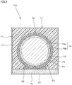
- Fig. 3 is a cross section of solid electrolytic capacitor 100 shown in Fig. 2 when cut along a cutting line III-III.
- Fig. 4 is a bottom view of solid electrolytic capacitor 100 shown in Fig. 1 .
- Solid electrolytic capacitor 100 in one embodiment includes a body 10 in the form of a rectangular parallelepiped, a first anode terminal 14 disposed on an end surface 11 on one side of body 10 and a second anode terminal 15 disposed on an end surface 12 on the other side of body 10, and a cathode terminal 16 disposed on a bottom surface 13 of body 10.
- First anode terminal 14 and second anode terminal 15 constitute a first external terminal
- cathode terminal 16 constitutes a second external terminal.
- Body 10 includes a capacitor element 18 and a sealing material 17 covering capacitor element 18.
- Capacitor element 18 includes a columnar metal core material 19 having a valve function.
- valve metal constituting metal core material 19 for example, aluminum, tantalum, niobium, titanium, or an alloy including at least one thereof is used.
- metal core material 19 has a circular columnar shape.
- metal core material 19 is not limited in shape to a circular columnar shape, and may for example be a rectangular columnar shape.
- An aluminum wire is preferably used as metal core material 19 in terms of low cost and availability.
- Metal core material 19 includes a core 19a extending in the axial direction of metal core material 19, and a porous layer 19b provided on a portion of a surface of core 19a.
- Porous layer 19b is formed for example by etching a surface of metal core material 19 made of aluminum wire to roughen the surface to be a rough surface.
- porous layer 19b has a large number of pores 20 formed to have an opening directed outward.
- Porous layer 19b has a pore diameter for example of 0.01 ⁇ m or more and 100 ⁇ m or less.
- porous layer 19b is a region surrounded by a dotted line and shaded.
- an area C1 of the end surface of metal core material 19 is larger than an area C2 of a cross section of a central portion of metal core material 19 in the lengthwise direction of metal core material 19, the cross section being orthogonal to the axial direction of metal core material 19 (see Fig. 2 ).
- area C1 of the end surface of metal core material 19 is 1% or more larger than area C2 of the cross section of the central portion of metal core material 19 in the lengthwise direction of metal core material 19.
- porous layer 19b has a surface provided with a dielectric layer 21 which is an oxide film. More specifically, dielectric layer 21 is formed along an inner peripheral surface of pore 20 of porous layer 19b. In Fig. 5 , dielectric layer 21 is indicated by a thick line.
- Dielectric layer 21 is formed, for example, by oxidizing a surface of metal core material 19 provided with porous layer 19b.
- Dielectric layer 21 is composed of oxide film having a thickness for example of 0.003 ⁇ m or more and 5 ⁇ m or less.
- Capacitor element 18 further includes a cathode layer 22 on dielectric layer 21.
- a ⁇ conjugated conductive polymer can be used as the conductive polymer included in conductive polymer layer 23 .
- the ⁇ conjugated conductive polymer include substituted or unsubstituted polypyrrole, polythiophene, polyaniline, polyacetylene, poly(p-phenylene), poly(p-phenylenevinylene) and poly(thienylenevinylene), and a derivative thereof.
- substituents examples include a hydrogen atom, a hydroxyl group, a carboxyl group, a nitro group, a phenyl group, a vinyl group, a halogen atom, an acyl group, an amino group, a sulfonic acid group, a sulfonyl group, a carboxylate group, a sulfonate group, an alkoxyl group, an alkylthio group, an arylthio group, an alkyl group of C1 to C18 which may have these substituents, a cycloalkyl group of C5 to C12 which may have these substituents, an aryl group of C6 to C14 which may have these substituents, and an aralkyl group of C7 to C18 which may have these substituents.
- the conductive polymer is preferably a conductive polymer including at least one selected from the group consisting of polypyrrole, polythiophene and polyaniline, and a derivative thereof. From the viewpoint of thermal stability, the conductive polymer more preferably includes a repeating unit of 3,4-ethylenedioxythiophene or a derivative thereof.
- the conductive polymer may be a homopolymer or a copolymer. These conductive polymers may be used each alone or in combination of two or more thereof.
- conductive polymer layer 23 is not particularly limited in thickness, for example, in a case where a low resistance is required, a thin film is preferable from the viewpoint of each layer's volume resistivity, and preferably it is adjusted to have a desired thickness depending on characteristics required as appropriate.
- conductive polymer layer 23 is provided so as to fill at least a portion of pores 20 of porous layer 19b. Although conductive polymer layer 23 does not necessarily cover the entire peripheral surface of porous layer 19b, conductive polymer layer 23 can be brought into contact with dielectric layer 21 over a large area when conductive polymer layer 23 covers the entire peripheral surface of porous layer 19b.
- the conductive polymer adhering to resist film 30, which will be described hereinafter, may be removed by a laser or the like, or a mask or the like may be disposed so that the conductive polymer is not applied to resist film 30. This ensures insulation between anode terminals 14 and 15 and cathode terminal 16.
- Carbon layer 24 and silver layer 25 of cathode layer 22 function as a cathode layer of capacitor element 18.
- the cathode layer may be any layer that is electrically conductive. While in the present embodiment the cathode layer is composed of a plurality of layers, that is, carbon layer 24 and silver layer 25, the cathode layer may be composed of silver layer 25 alone.
- Porous layer 19b is electrically connected to cathode terminal 16 via cathode layer 22.
- Cathode layer 22, more specifically, silver layer 25, is connected to cathode terminal 16 via a conductive adhesive 26 (see Fig. 3 ).
- Metal core material 19 has core 19a with opposite end surfaces exposed from sealing material 17. An end surface on one side of metal core material 19 is connected to first anode terminal 14, and an end surface on the other side of metal core material 19 is connected to second anode terminal 15.
- First anode terminal 14 and second anode terminal 15 are each composed of a plating film or a conductive resin film formed on the end surface of core 19a of metal core material 19.
- the plating film includes, for example, a metal such as nickel, zinc, copper, tin, gold, silver, palladium or lead, or an alloy containing at least one of these metals.
- the conductive resin film includes resin such as epoxy, and metal particles of at least one type for example of silver, copper, nickel, tin and palladium in the resin as a conductive component.
- First anode terminal 14 and second anode terminal 15 may each have a multilayer structure including a plating film and a conductive resin film.
- first anode terminal 14 and second anode terminal 15 may each include two plating layers and a conductive resin layer between the plating layers.
- a resist film 30 made of an electrically insulating resin is disposed on the surface of metal core material 19 in a region free of porous layer 19b.
- Resist film 30 is, for example, a resin including at least one of polyimide and epoxy.
- a step is not essential between resist film 30 and cathode layer 22.
- Cathode layer 22 may be larger in thickness than resist film 30.
- Resist film 30 may have a portion covering cathode layer 22.
- Sealing material 17 includes resin.
- sealing material 17 may include alumina, silica or a similar filler, or a magnetic material.
- sealing material 17 can be adjusted in mechanical strength and workability. Furthermore, selecting a filler having a desired coefficient of linear expansion allows adjustment in heat shrinkability.
- sealing material 17 includes a magnetic material
- the capacitor's impedance can be intentionally increased.
- antiresonance may occur when a plurality of capacitors having low impedance are mounted in parallel.
- the sealing material includes a magnetic material
- antiresonance can be suppressed.
- the magnetic material for example, magnetic powder such as iron powder, iron-containing alloy powder, or ferrite powder is used.
- the magnetic material may be a mixture of two or more types of powder of different particle sizes or different compositions. As has been discussed above, for sealing material 17, it is preferable to select and use a desired filler, magnetic material or the like depending on the required function.
- An aluminum wire is prepared as columnar metal core material 19 having a valve function (step S1 in Fig. 6 ).
- the aluminum wire has a diameter for example of 0.02 mm or more and 5.0 mm or less.
- the aluminum wire is not particularly limited in shape and may have a circular columnar shape or a rectangular columnar shape.
- resist film 30 is disposed at predetermined intervals L1 in the lengthwise direction of the aluminum wire serving as metal core material 19 (step S2 in Fig. 6 ).
- resist film 30 for example, one of a polyimide resin and an epoxy resin can be used.
- resist film 30 is disposed on the surface of the aluminum wire in predetermined regions at predetermined intervals L1.
- predetermined interval L1 is for example 0.1 mm or more and 3.0 mm or less.
- the predetermined region in which resist film 30 is disposed has a length for example of 0.1 mm or more and 3.0 mm or less.
- step S2 in Fig. 6 there may be provided the steps of: disposing resist film 30 on the entire surface of the aluminum wire serving as metal core material 19; and removing resist film 30 in such a manner that resist film 30 of a predetermined region remains for each predetermined interval L1 in the lengthwise direction of the aluminum wire.
- the aluminum wire has a surface etched to form porous layer 19b (step S3 in Fig. 6 ). As shown in Fig. 7(b) , porous layer 19b is formed in a region free of resist film 30.
- the aluminum wire has the surface etched for example in a method such as alternate-current electrolytic etching, direct-current electrolytic etching, chemical corrosion, or the like.
- the aluminum wire has a surface etched to form porous layer 19b in a region free of resist film 30.
- the aluminum wire is divided at the location of resist film 30 into individual pieces, and therefore, in a finally manufactured solid electrolytic capacitor, the location of resist film 30 will be an end portion of metal core material 19.
- area C1 of an end surface of metal core material 19 will be larger than area C2 of the cross section of the central portion of metal core material 19.
- dielectric layer 21 is formed on a surface of the aluminum wire by chemical conversion treatment (step S4 in Fig. 6 ).
- the chemical conversion treatment ammonium adipate, for example, is used as a chemical conversion liquid. That is, the aluminum wire has a surface electrochemically oxidized in an aqueous solution of ammonium adipate to form an oxide film constituting dielectric layer 21. The region in which resist film 30 is disposed is not in contact with the chemical conversion liquid, and the oxide film is not formed.
- the chemical conversion treatment may be performed after resist film 30 is removed by a laser or the like.
- the oxide film formed in the region in which resist film 30 was disposed may be removed by the laser or the like, or may not be removed and instead remain as it is.
- a material including a conductive polymer is applied to a surface of the aluminum wire (step S5 in Fig. 6 ). Specifically, a conductive polymer solution with poly(3,4-ethylenedioxythiophene) dispersed therein is applied while it is caused to penetrate through porous layer 19b, and thereafter the conductive polymer solution is dried to form conductive polymer layer 23 as a solid electrolyte.
- the aluminum wire is immersed in the conductive polymer solution.
- Conductive polymer layer 23 is not formed on the surface of the aluminum wire in a region in which resist film 30 is disposed.
- the conductive polymer solution may selectively be applied on porous layer 19b.
- the material including the conductive polymer adheres to the surface of metal core material 19 in a region free of porous layer 19b
- the material including the conductive polymer that adheres to the region may be removed by a laser or the like.
- Carbon layer 24 is formed on conductive polymer layer 23 (step S6 in Fig. 6 ).
- Carbon layer 24 can be formed in a method for example of coating, immersing, printing, transferring, or the like for example using carbon paste.
- silver layer 25 is formed on carbon layer 24 (step S7 in Fig. 6 ).
- Silver layer 25 can be formed in a method for example of coating, immersing, printing, transferring, or the like for example using silver paste.
- conductive polymer layer 23, carbon layer 24, and silver layer 25 constitute cathode layer 22 (see Fig. 7(c) ).
- a substrate on which an electrode to be cathode terminal 16 is disposed is prepared, and the electrode to be cathode terminal 16 and cathode layer 22 are bonded by using conductive adhesive 26 (step S8 in Fig. 6 ).
- metal core material 19 is peripherally molded with resin in such a manner that a surface of cathode terminal 16 that faces outward and the opposite end surfaces of metal core material 19 are exposed (step S9 in Fig. 6 ).
- This resin constitutes sealing material 17.
- the aluminum wire is divided at the location of resist film 30 into individual pieces (step S10 in Fig. 6 ). More specifically, the aluminum wire is divided at a central position of resist film 30 in the lengthwise direction of the aluminum wire, as indicated in Fig. 7(c) by a broken line, into individual pieces (see Fig. 7(d) ). This can be done in any method, such as dicing, press-cutting, or cutting a slit on a surface to divide the aluminum wire.
- first anode terminal 14 and second anode terminal 15 are formed so as to be connected to the opposite end surfaces of metal core material 19 exposed from sealing material 17 (step S1 in Fig. 6 ).
- First anode terminal 14 and second anode terminal 15 are formed for example by plating the opposite end surfaces of metal core material 19. This can be done for example by electrolytic plating or electroless plating.
- an aluminum wire is used as metal core material 19, and accordingly, in order to form a closely adhesive plating film, a zincate treatment is initially performed and plating is subsequently performed. Specifically, a Pd containing solution is applied to metal core material 19, a zincate treatment is performed to precipitate Ni through substitution, and Sn plating is applied on Ni plating.
- solid electrolytic capacitor 100 can be manufactured (see Fig. 7(e) ).
- a plurality of types of solid electrolytic capacitors having different ratios K of area C1 of the end surface of metal core material 19 to area C2 of the cross section of the center portion of metal core material 19 were fabricated.
- the plurality of types of solid electrolytic capacitors had their ESRs measured with a measuring instrument (E4980A) manufactured by KEY SIGHT TECHNOLOGIES.
- Table 1 shows a relationship between ratio K of area C1 of the end surface of metal core material 19 to area C2 of the cross section of the center portion of metal core material 19 and ESR.
- Table 1 ratio K (%) end surface's area C1/central portion's cross-sectional area C2)
- ESR (m ⁇ ) 0.99 271 1.00 270 1.01 253 1.02 251 1.10 246 1.29 229 1.50 198
Landscapes
- Engineering & Computer Science (AREA)
- Power Engineering (AREA)
- Microelectronics & Electronic Packaging (AREA)
- Chemical & Material Sciences (AREA)
- Manufacturing & Machinery (AREA)
- Materials Engineering (AREA)
- Chemical Kinetics & Catalysis (AREA)
- Electrochemistry (AREA)
- Fixed Capacitors And Capacitor Manufacturing Machines (AREA)
Abstract
Description
- The present invention relates to a solid electrolytic capacitor and a method for manufacturing the same.
- A solid electrolytic capacitor is advantageously used not only as a typical capacitor in a decoupling circuit, a power supply circuit and the like but also as a noise filter for removing high-frequency noise.
- As an example of a solid electrolytic capacitor,
PTL 1 discloses a solid electrolytic capacitor having a structure in which an anode lead wire is led to an end surface of a capacitor element and an external electrode is formed on the end surface of the capacitor element so as to be connected to the anode lead wire. The external electrode is connected to an end surface of the anode lead wire. - PTL 1: Japanese Patent Laid-Open No.
2009-094475 - However, the solid electrolytic capacitor described in
PTL 1 has the anode lead wire and the external electrode with a small connection area therebetween, which increases connection resistance, and a large equivalent series resistance (ESR) is provided, which is a problem. - The present invention solves the above problem, and an object of the present invention is to provide a solid electrolytic capacitor with reduced ESR, and a method for manufacturing such a solid electrolytic capacitor.
- According to the present invention, a solid electrolytic capacitor comprises: a columnar metal core material having a valve function; first external terminals connected to an end surface on one side of the metal core material and an end surface on the other side of the metal core material, respectively; and a second external terminal different in polarity from the first external terminals, the end surface of the metal core material having an area larger than that of a cross section of a central portion of the metal core material in a lengthwise direction of the metal core material, the cross section being orthogonal to an axial direction of the metal core material, the metal core material having a surface partially provided with a porous layer including an oxide film, the porous layer being connected to the second external terminal via a cathode layer that is a conductive layer including a conductive polymer.
- The area of the end surface of the metal core material may be larger than that of the cross section of the central portion by 1% or more.
- A resist film may be disposed on the surface of the metal core material at a portion free of the porous layer.
- The resist film may be a resin including at least one of polyimide and epoxy.
- According to the present invention, a method for manufacturing a solid electrolytic capacitor comprises: preparing a columnar metal core material having a valve function; disposing a resist film on a surface of the metal core material; removing the resist film in such a manner that the resist film is disposed at predetermined intervals in a lengthwise direction of the metal core material; forming a porous layer on the surface of the metal core material at a portion free of the resist film; subjecting the porous layer to a chemical conversion treatment; applying a material including a conductive polymer to the surface of the metal core material after the chemical conversion treatment to form a conductive polymer layer; dividing the metal core material at a location of the resist film into individual pieces; and providing each individual piece with external terminals on opposite end surfaces of the metal core material.
- According to the present invention, a method for manufacturing a solid electrolytic capacitor comprises: preparing a columnar metal core material having a valve function; disposing a resist film on a surface of the metal core material at predetermined intervals in a lengthwise direction of the metal core material; forming a porous layer on the surface of the metal core material at a portion free of the resist film; subjecting the porous layer to a chemical conversion treatment; applying a material including a conductive polymer to the surface of the metal core material after the chemical conversion treatment to form a conductive polymer layer; dividing the metal core material at a location of the resist film into individual pieces; and providing each individual piece with external terminals on opposite end surfaces of the metal core material.
- The resist film may be a resin including at least one of polyimide and epoxy.
- The method for manufacturing a solid electrolytic capacitor may further comprise: forming a carbon layer on the conductive polymer layer; and forming a silver layer on the carbon layer.
- A solid electrolytic capacitor of the present invention is configured such that first external terminals are connected to opposite end surfaces of a metal core material and the end surface of the metal core material has an area larger than that of a cross section of a central portion of the metal core material in the lengthwise direction of the metal core material, and a connection area of the metal core material and the first external terminal can thus be increased. Such a configuration can reduce ESR.
- In a method for manufacturing a solid electrolytic capacitor according to the present invention, after a resist film is disposed on a surface of a metal core material, the resist film is removed in such a manner that the resist film is disposed at predetermined intervals, and a porous layer is formed on the surface of the metal core material at a portion free of the resist film. Then, the metal core material is divided at the location of the resist film into individual pieces, and each individual piece is provided with external terminals on opposite end surfaces of the metal core material. The end surface of the metal core material has an area larger than that of a cross section of a central portion of the metal core material in the lengthwise direction of the metal core material, and a connection area of the metal core material and the first external terminal can be increased, and accordingly, ESR can be reduced.
- Furthermore, in a method for manufacturing a solid electrolytic capacitor according to the present invention, a resist film is disposed on a surface of a metal core material at predetermined intervals in the lengthwise direction of the metal core material, and a porous layer is formed on the surface of the metal core material at a portion free of the resist film. Then, the metal core material is divided at the location of the resist film into individual pieces, and each individual piece is provided with external terminals on opposite end surfaces of the metal core material. The end surface of the metal core material has an area larger than that of a cross section of a central portion of the metal core material in the lengthwise direction of the metal core material, and a connection area of the metal core material and the first external terminal can be increased and accordingly, ESR can be reduced.
-
-
Fig. 1 is a perspective view showing an appearance of a solid electrolytic capacitor according to an embodiment. -
Fig. 2 is a cross section of the solid electrolytic capacitor shown inFig. 1 taken along a line II-II. -
Fig. 3 is a cross section of the solid electrolytic capacitor shown inFig. 2 taken along a line III-III. -
Fig. 4 is a bottom view of the solid electrolytic capacitor shown inFig. 1 . -
Fig. 5 is a schematic cross section enlarging a portion V ofFig. 2 . -
Fig. 6 is a flowchart of a process for manufacturing a solid electrolytic capacitor according to an embodiment. -
Fig. 7 is a diagram for illustrating a method for manufacturing a solid electrolytic capacitor. - Hereinafter, what is a feature of the present invention will specifically be described with reference to an embodiment of the present invention.
-
Fig. 1 is a perspective view showing an appearance of a solidelectrolytic capacitor 100 according to an embodiment.Fig. 2 is a cross section of solidelectrolytic capacitor 100 shown inFig. 1 when cut along a cutting line II-II, andFig. 3 is a cross section of solidelectrolytic capacitor 100 shown inFig. 2 when cut along a cutting line III-III.Fig. 4 is a bottom view of solidelectrolytic capacitor 100 shown inFig. 1 . - Solid
electrolytic capacitor 100 in one embodiment includes abody 10 in the form of a rectangular parallelepiped, afirst anode terminal 14 disposed on anend surface 11 on one side ofbody 10 and asecond anode terminal 15 disposed on anend surface 12 on the other side ofbody 10, and acathode terminal 16 disposed on abottom surface 13 ofbody 10.First anode terminal 14 andsecond anode terminal 15 constitute a first external terminal, andcathode terminal 16 constitutes a second external terminal. -
Body 10 includes acapacitor element 18 and a sealingmaterial 17 coveringcapacitor element 18. -
Capacitor element 18 includes a columnarmetal core material 19 having a valve function. As valve metal constitutingmetal core material 19, for example, aluminum, tantalum, niobium, titanium, or an alloy including at least one thereof is used. - In the present embodiment,
metal core material 19 has a circular columnar shape. However,metal core material 19 is not limited in shape to a circular columnar shape, and may for example be a rectangular columnar shape. An aluminum wire is preferably used asmetal core material 19 in terms of low cost and availability. -
Metal core material 19 includes acore 19a extending in the axial direction ofmetal core material 19, and aporous layer 19b provided on a portion of a surface ofcore 19a. -
Porous layer 19b is formed for example by etching a surface ofmetal core material 19 made of aluminum wire to roughen the surface to be a rough surface. - As schematically shown in
Fig. 5 ,porous layer 19b has a large number ofpores 20 formed to have an opening directed outward.Porous layer 19b has a pore diameter for example of 0.01 µm or more and 100 µm or less. InFig. 3 ,porous layer 19b is a region surrounded by a dotted line and shaded. - In the present embodiment, an area C1 of the end surface of
metal core material 19 is larger than an area C2 of a cross section of a central portion ofmetal core material 19 in the lengthwise direction ofmetal core material 19, the cross section being orthogonal to the axial direction of metal core material 19 (seeFig. 2 ). Preferably, area C1 of the end surface ofmetal core material 19 is 1% or more larger than area C2 of the cross section of the central portion ofmetal core material 19 in the lengthwise direction ofmetal core material 19. When area C1 of the end surface ofmetal core material 19 is larger than area C2 of the cross section of the central portion ofmetal core material 19, a connection area ofmetal core material 19 andfirst anode terminal 14 and that ofmetal core material 19 andsecond anode terminal 15 are increased, and accordingly, ESR can be reduced. Furthermore, when area C1 of the end surface ofmetal core material 19 is larger than area C2 of the cross section of the central section ofmetal core material 19 by 1% or more, ESR can be effectively reduced. - As shown in
Fig. 5 ,porous layer 19b has a surface provided with adielectric layer 21 which is an oxide film. More specifically,dielectric layer 21 is formed along an inner peripheral surface ofpore 20 ofporous layer 19b. InFig. 5 ,dielectric layer 21 is indicated by a thick line. -
Dielectric layer 21 is formed, for example, by oxidizing a surface ofmetal core material 19 provided withporous layer 19b.Dielectric layer 21 is composed of oxide film having a thickness for example of 0.003 µm or more and 5 µm or less. -
Capacitor element 18 further includes acathode layer 22 ondielectric layer 21.Cathode layer 22, which is a conductive layer, includes aconductive polymer layer 23 as a solid electrolyte, acarbon layer 24 onconductive polymer layer 23, and asilver layer 25 oncarbon layer 24. - As the conductive polymer included in
conductive polymer layer 23, a π conjugated conductive polymer can be used. Examples of the π conjugated conductive polymer include substituted or unsubstituted polypyrrole, polythiophene, polyaniline, polyacetylene, poly(p-phenylene), poly(p-phenylenevinylene) and poly(thienylenevinylene), and a derivative thereof. - Examples of the substituent include a hydrogen atom, a hydroxyl group, a carboxyl group, a nitro group, a phenyl group, a vinyl group, a halogen atom, an acyl group, an amino group, a sulfonic acid group, a sulfonyl group, a carboxylate group, a sulfonate group, an alkoxyl group, an alkylthio group, an arylthio group, an alkyl group of C1 to C18 which may have these substituents, a cycloalkyl group of C5 to C12 which may have these substituents, an aryl group of C6 to C14 which may have these substituents, and an aralkyl group of C7 to C18 which may have these substituents.
- Inter alia, the conductive polymer is preferably a conductive polymer including at least one selected from the group consisting of polypyrrole, polythiophene and polyaniline, and a derivative thereof. From the viewpoint of thermal stability, the conductive polymer more preferably includes a repeating unit of 3,4-ethylenedioxythiophene or a derivative thereof. The conductive polymer may be a homopolymer or a copolymer. These conductive polymers may be used each alone or in combination of two or more thereof.
- Although
conductive polymer layer 23 is not particularly limited in thickness, for example, in a case where a low resistance is required, a thin film is preferable from the viewpoint of each layer's volume resistivity, and preferably it is adjusted to have a desired thickness depending on characteristics required as appropriate. - As shown in
Fig. 5 ,conductive polymer layer 23 is provided so as to fill at least a portion ofpores 20 ofporous layer 19b. Althoughconductive polymer layer 23 does not necessarily cover the entire peripheral surface ofporous layer 19b,conductive polymer layer 23 can be brought into contact withdielectric layer 21 over a large area whenconductive polymer layer 23 covers the entire peripheral surface ofporous layer 19b. The conductive polymer adhering to resistfilm 30, which will be described hereinafter, may be removed by a laser or the like, or a mask or the like may be disposed so that the conductive polymer is not applied to resistfilm 30. This ensures insulation betweenanode terminals cathode terminal 16. -
Carbon layer 24 andsilver layer 25 ofcathode layer 22 function as a cathode layer ofcapacitor element 18. The cathode layer may be any layer that is electrically conductive. While in the present embodiment the cathode layer is composed of a plurality of layers, that is,carbon layer 24 andsilver layer 25, the cathode layer may be composed ofsilver layer 25 alone. -
Porous layer 19b is electrically connected tocathode terminal 16 viacathode layer 22.Cathode layer 22, more specifically,silver layer 25, is connected tocathode terminal 16 via a conductive adhesive 26 (seeFig. 3 ). -
Metal core material 19 hascore 19a with opposite end surfaces exposed from sealingmaterial 17. An end surface on one side ofmetal core material 19 is connected tofirst anode terminal 14, and an end surface on the other side ofmetal core material 19 is connected tosecond anode terminal 15. -
First anode terminal 14 andsecond anode terminal 15 are each composed of a plating film or a conductive resin film formed on the end surface ofcore 19a ofmetal core material 19. The plating film includes, for example, a metal such as nickel, zinc, copper, tin, gold, silver, palladium or lead, or an alloy containing at least one of these metals. The conductive resin film includes resin such as epoxy, and metal particles of at least one type for example of silver, copper, nickel, tin and palladium in the resin as a conductive component. -
First anode terminal 14 andsecond anode terminal 15 may each have a multilayer structure including a plating film and a conductive resin film. For example,first anode terminal 14 andsecond anode terminal 15 may each include two plating layers and a conductive resin layer between the plating layers. - A resist
film 30 made of an electrically insulating resin is disposed on the surface ofmetal core material 19 in a region free ofporous layer 19b. Resistfilm 30 is, for example, a resin including at least one of polyimide and epoxy. A step is not essential between resistfilm 30 andcathode layer 22.Cathode layer 22 may be larger in thickness than resistfilm 30. Resistfilm 30 may have a portion coveringcathode layer 22. - Sealing
material 17 includes resin. In addition to resin, sealingmaterial 17 may include alumina, silica or a similar filler, or a magnetic material. When sealingmaterial 17 includes the filler, sealingmaterial 17 can be adjusted in mechanical strength and workability. Furthermore, selecting a filler having a desired coefficient of linear expansion allows adjustment in heat shrinkability. - When sealing
material 17 includes a magnetic material, the capacitor's impedance can be intentionally increased. For example, antiresonance may occur when a plurality of capacitors having low impedance are mounted in parallel. In that case, when the sealing material includes a magnetic material, antiresonance can be suppressed. As the magnetic material, for example, magnetic powder such as iron powder, iron-containing alloy powder, or ferrite powder is used. The magnetic material may be a mixture of two or more types of powder of different particle sizes or different compositions. As has been discussed above, for sealingmaterial 17, it is preferable to select and use a desired filler, magnetic material or the like depending on the required function. - A method for manufacturing solid
electrolytic capacitor 100 having the above-described structure will be described with reference toFigs. 6 and7 . - An aluminum wire is prepared as columnar
metal core material 19 having a valve function (step S1 inFig. 6 ). The aluminum wire has a diameter for example of 0.02 mm or more and 5.0 mm or less. As has been discussed above, the aluminum wire is not particularly limited in shape and may have a circular columnar shape or a rectangular columnar shape. - Subsequently, as shown in
Fig. 7(a) , resistfilm 30 is disposed at predetermined intervals L1 in the lengthwise direction of the aluminum wire serving as metal core material 19 (step S2 inFig. 6 ). As resistfilm 30, for example, one of a polyimide resin and an epoxy resin can be used. Thus, resistfilm 30 is disposed on the surface of the aluminum wire in predetermined regions at predetermined intervals L1. - Herein, predetermined interval L1 is for example 0.1 mm or more and 3.0 mm or less. The predetermined region in which resist
film 30 is disposed has a length for example of 0.1 mm or more and 3.0 mm or less. - Instead of step S2 in
Fig. 6 , there may be provided the steps of: disposing resistfilm 30 on the entire surface of the aluminum wire serving asmetal core material 19; and removing resistfilm 30 in such a manner that resistfilm 30 of a predetermined region remains for each predetermined interval L1 in the lengthwise direction of the aluminum wire. - Subsequently, the aluminum wire has a surface etched to form
porous layer 19b (step S3 inFig. 6 ). As shown inFig. 7(b) ,porous layer 19b is formed in a region free of resistfilm 30. The aluminum wire has the surface etched for example in a method such as alternate-current electrolytic etching, direct-current electrolytic etching, chemical corrosion, or the like. - As has been described above, the aluminum wire has a surface etched to form
porous layer 19b in a region free of resistfilm 30. In a subsequent step, the aluminum wire is divided at the location of resistfilm 30 into individual pieces, and therefore, in a finally manufactured solid electrolytic capacitor, the location of resistfilm 30 will be an end portion ofmetal core material 19. Thus, by the above-described process, area C1 of an end surface ofmetal core material 19 will be larger than area C2 of the cross section of the central portion ofmetal core material 19. - Subsequently,
dielectric layer 21 is formed on a surface of the aluminum wire by chemical conversion treatment (step S4 inFig. 6 ). In the chemical conversion treatment, ammonium adipate, for example, is used as a chemical conversion liquid. That is, the aluminum wire has a surface electrochemically oxidized in an aqueous solution of ammonium adipate to form an oxide film constitutingdielectric layer 21. The region in which resistfilm 30 is disposed is not in contact with the chemical conversion liquid, and the oxide film is not formed. - The chemical conversion treatment may be performed after resist
film 30 is removed by a laser or the like. In that case, the oxide film formed in the region in which resistfilm 30 was disposed may be removed by the laser or the like, or may not be removed and instead remain as it is. - Subsequently, a material including a conductive polymer is applied to a surface of the aluminum wire (step S5 in
Fig. 6 ). Specifically, a conductive polymer solution with poly(3,4-ethylenedioxythiophene) dispersed therein is applied while it is caused to penetrate throughporous layer 19b, and thereafter the conductive polymer solution is dried to formconductive polymer layer 23 as a solid electrolyte. - Herein, in order to fill
pores 20 ofporous layer 19b with the material including the conductive polymer, the aluminum wire is immersed in the conductive polymer solution.Conductive polymer layer 23 is not formed on the surface of the aluminum wire in a region in which resistfilm 30 is disposed. - Note that the conductive polymer solution may selectively be applied on
porous layer 19b. - When the material including the conductive polymer adheres to the surface of
metal core material 19 in a region free ofporous layer 19b, the material including the conductive polymer that adheres to the region may be removed by a laser or the like. - Subsequently,
carbon layer 24 is formed on conductive polymer layer 23 (step S6 inFig. 6 ).Carbon layer 24 can be formed in a method for example of coating, immersing, printing, transferring, or the like for example using carbon paste. - Subsequently,
silver layer 25 is formed on carbon layer 24 (step S7 inFig. 6 ).Silver layer 25 can be formed in a method for example of coating, immersing, printing, transferring, or the like for example using silver paste. - As has been described above,
conductive polymer layer 23,carbon layer 24, andsilver layer 25 constitute cathode layer 22 (seeFig. 7(c) ). - Subsequently, a substrate on which an electrode to be
cathode terminal 16 is disposed is prepared, and the electrode to becathode terminal 16 andcathode layer 22 are bonded by using conductive adhesive 26 (step S8 inFig. 6 ). - Then,
metal core material 19 is peripherally molded with resin in such a manner that a surface ofcathode terminal 16 that faces outward and the opposite end surfaces ofmetal core material 19 are exposed (step S9 inFig. 6 ). This resin constitutes sealingmaterial 17. - Subsequently, the aluminum wire is divided at the location of resist
film 30 into individual pieces (step S10 inFig. 6 ). More specifically, the aluminum wire is divided at a central position of resistfilm 30 in the lengthwise direction of the aluminum wire, as indicated inFig. 7(c) by a broken line, into individual pieces (seeFig. 7(d) ). This can be done in any method, such as dicing, press-cutting, or cutting a slit on a surface to divide the aluminum wire. - Subsequently, for each individual piece,
first anode terminal 14 andsecond anode terminal 15 are formed so as to be connected to the opposite end surfaces ofmetal core material 19 exposed from sealing material 17 (step S1 inFig. 6 ).First anode terminal 14 andsecond anode terminal 15 are formed for example by plating the opposite end surfaces ofmetal core material 19. This can be done for example by electrolytic plating or electroless plating. - Note that aluminum has a property allowing oxide film to be easily formed, and oxide film can be a factor to prevent close adhesion of a plating film. In the present embodiment, an aluminum wire is used as
metal core material 19, and accordingly, in order to form a closely adhesive plating film, a zincate treatment is initially performed and plating is subsequently performed. Specifically, a Pd containing solution is applied tometal core material 19, a zincate treatment is performed to precipitate Ni through substitution, and Sn plating is applied on Ni plating. - Through the above-described process, solid
electrolytic capacitor 100 can be manufactured (seeFig. 7(e) ). - By the above method, a plurality of types of solid electrolytic capacitors having different ratios K of area C1 of the end surface of
metal core material 19 to area C2 of the cross section of the center portion ofmetal core material 19 were fabricated. The plurality of types of solid electrolytic capacitors had their ESRs measured with a measuring instrument (E4980A) manufactured by KEY SIGHT TECHNOLOGIES. - After the ESR measurement, ratio K of area C1 of the end surface of
metal core material 19 to area C2 of the cross section of the central portion of metal core material 19 (i.e., K = C1/C2) was determined. - Herein, ten solid electrolytic capacitors were prepared for each of the plurality of types of solid electrolytic capacitors having different ratios K and their respective ESRs and ratios K were obtained, and the ten solid electrolytic capacitors' average ESR and ratio K values were obtained.
- Table 1 shows a relationship between ratio K of area C1 of the end surface of
metal core material 19 to area C2 of the cross section of the center portion ofmetal core material 19 and ESR.Table 1 ratio K (%) (end surface's area C1/central portion's cross-sectional area C2) ESR (mΩ) 0.99 271 1.00 270 1.01 253 1.02 251 1.10 246 1.29 229 1.50 198 - As shown in Table 1, with reference to area C2 of the cross section of the central portion of
metal core material 19 being equal to area C1 of the end surface ofmetal core material 19, that is, with a ratio K of 1 serving a reference, for a ratio K larger than 1, a reduced ESR was provided. For example, for a ratio K of 1, an ESR of 270 mΩ was provided, and for a ratio K of 1.01, that is, when area C1 of the end surface ofmetal core material 19 was 1% larger than area C2 of the cross section of the central portion ofmetal core material 19, an ESR of 253 mΩ was provided. As ratio K increases, that is, as area C1 of the end surface ofmetal core material 19 increases relative to area C2 of the cross section of the center portion ofmetal core material 19, ESR decreases. - The present invention is not limited to the above embodiment, and a variety of types of applications and modifications can be made within the scope of the present invention.
-
- 10
- body
- 11
- end surface of one side of the body
- 12
- end surface of the other side of the body
- 13
- bottom surface of the body
- 14
- first anode terminal
- 15
- second anode terminal
- 16
- cathode terminal
- 17
- sealing material
- 18
- capacitor element
- 19
- metal core material
- 19a
- core
- 19b
- porous layer
- 20
- pore
- 21
- dielectric layer
- 22
- cathode layer
- 23
- conductive polymer layer
- 24
- carbon layer
- 25
- silver layer
- 26
- conductive adhesive
- 30
- resist film
- 100
- solid electrolytic capacitor
Claims (8)
- A solid electrolytic capacitor comprising:a columnar metal core material having a valve function;first external terminals connected to an end surface on one side of the metal core material and an end surface on the other side of the metal core material, respectively; anda second external terminal different in polarity from the first external terminals,the end surface of the metal core material having an area larger than that of a cross section of a central portion of the metal core material in a lengthwise direction of the metal core material, the cross section being orthogonal to an axial direction of the metal core material,the metal core material having a surface partially provided with a porous layer including an oxide film,the porous layer being connected to the second external terminal via a cathode layer that is a conductive layer including a conductive polymer.
- The solid electrolytic capacitor according to claim 1, wherein the area of the end surface of the metal core material is larger than that of the cross section of the central portion of the metal core material by 1% or more.
- The solid electrolytic capacitor according to claim 1 or 2, wherein a resist film is disposed on the surface of the metal core material at a portion free of the porous layer.
- The solid electrolytic capacitor according to claim 3, wherein the resist film is a resin including at least one of polyimide and epoxy.
- A method for manufacturing a solid electrolytic capacitor, comprising:preparing a columnar metal core material having a valve function;disposing a resist film on a surface of the metal core material;removing the resist film in such a manner that the resist film is disposed at predetermined intervals in a lengthwise direction of the metal core material;forming a porous layer on the surface of the metal core material at a portion free of the resist film;subjecting the porous layer to a chemical conversion treatment;applying a material including a conductive polymer to the surface of the metal core material after the chemical conversion treatment to form a conductive polymer layer;dividing the metal core material at a location of the resist film into individual pieces; andproviding each individual piece with external terminals on opposite end surfaces of the metal core material.
- A method for manufacturing a solid electrolytic capacitor, comprising:preparing a columnar metal core material having a valve function;disposing a resist film on a surface of the metal core material at predetermined intervals in a lengthwise direction of the metal core material;forming a porous layer on the surface of the metal core material at a portion free of the resist film;subjecting the porous layer to a chemical conversion treatment;applying a material including a conductive polymer to the surface of the metal core material after the chemical conversion treatment to form a conductive polymer layer;dividing the metal core material at a location of the resist film into individual pieces; andproviding each individual piece with external terminals on opposite end surfaces of the metal core material.
- The method for manufacturing a solid electrolytic capacitor according to claim 5 or 6, wherein the resist film is a resin including at least one of polyimide and epoxy.
- The method for manufacturing a solid electrolytic capacitor according to any one of claims 5 to 7, further comprising:forming a carbon layer on the conductive polymer layer; andforming a silver layer on the carbon layer.
Applications Claiming Priority (2)
| Application Number | Priority Date | Filing Date | Title |
|---|---|---|---|
| JP2018045580 | 2018-03-13 | ||
| PCT/JP2019/009092 WO2019176723A1 (en) | 2018-03-13 | 2019-03-07 | Solid electrolytic capacitor and method for manufacturing solid electrolytic capacitor |
Publications (2)
| Publication Number | Publication Date |
|---|---|
| EP3767654A1 true EP3767654A1 (en) | 2021-01-20 |
| EP3767654A4 EP3767654A4 (en) | 2022-01-05 |
Family
ID=67907199
Family Applications (1)
| Application Number | Title | Priority Date | Filing Date |
|---|---|---|---|
| EP19767469.0A Pending EP3767654A4 (en) | 2018-03-13 | 2019-03-07 | SOLID ELECTROLYTIC CAPACITOR AND METHOD FOR MANUFACTURING SOLID ELECTROLYTIC CAPACITOR |
Country Status (5)
| Country | Link |
|---|---|
| US (1) | US11270846B2 (en) |
| EP (1) | EP3767654A4 (en) |
| JP (1) | JP7465547B2 (en) |
| CN (2) | CN111837211B (en) |
| WO (1) | WO2019176723A1 (en) |
Families Citing this family (3)
| Publication number | Priority date | Publication date | Assignee | Title |
|---|---|---|---|---|
| CN114830275B (en) * | 2019-12-18 | 2024-06-28 | 株式会社村田制作所 | Solid electrolytic capacitors |
| WO2021205894A1 (en) * | 2020-04-10 | 2021-10-14 | 株式会社村田製作所 | Electrolytic capacitor and method for manufacturing electrolytic capacitor |
| FR3120982A1 (en) * | 2021-03-18 | 2022-09-23 | Commissariat A L'energie Atomique Et Aux Energies Alternatives | HIGH DENSITY CAPACITIVE DEVICE AND METHOD FOR FABRICATING SUCH A DEVICE |
Family Cites Families (16)
| Publication number | Priority date | Publication date | Assignee | Title |
|---|---|---|---|---|
| JPS266076B1 (en) * | 1950-08-11 | 1951-10-09 | ||
| JPS5175954A (en) * | 1974-12-26 | 1976-06-30 | New Nippon Electric Co | |
| JPH0684716A (en) * | 1992-08-31 | 1994-03-25 | Nippon Chemicon Corp | Manufacture of solid electrolytic capacitor |
| JP2000082640A (en) * | 1998-09-07 | 2000-03-21 | Matsushita Electric Ind Co Ltd | Aluminum electrolytic capacitor and method of manufacturing the same |
| CN1950915A (en) * | 2004-04-27 | 2007-04-18 | 昭和电工株式会社 | Mamufacturing method of capacitor electrode foil, capacitor electrode foil, laminate type electrolytic capacitor and winding type electrolytic capacitor |
| JP5128053B2 (en) | 2004-04-27 | 2013-01-23 | 昭和電工株式会社 | Capacitor electrode foil manufacturing method, capacitor electrode foil, multilayer electrolytic capacitor, and wound electrolytic capacitor |
| JP2006005309A (en) * | 2004-06-21 | 2006-01-05 | Shinko Electric Ind Co Ltd | Capacitor device |
| JP4739148B2 (en) * | 2005-08-29 | 2011-08-03 | Necトーキン株式会社 | Solid electrolytic capacitor |
| JP2009094475A (en) | 2007-09-19 | 2009-04-30 | Panasonic Corp | Chip type solid electrolytic capacitor |
| US8159811B2 (en) * | 2007-10-19 | 2012-04-17 | Oh Young Joo | Metal capacitor and manufacturing method thereof |
| JP2009267232A (en) * | 2008-04-28 | 2009-11-12 | Shin Etsu Polymer Co Ltd | Capacitor, and manufacturing method thereof |
| JP2010239065A (en) | 2009-03-31 | 2010-10-21 | Nippon Chemicon Corp | Method of manufacturing solid electrolytic capacitor |
| CN103430261B (en) * | 2011-04-20 | 2016-08-17 | 株式会社村田制作所 | The manufacture method of solid electrolytic capacitor and solid electrolytic capacitor |
| TWI431650B (en) * | 2011-07-18 | 2014-03-21 | Apaq Technology Co Ltd | Method for manufacturing solid electrolytic capacitor and solid electrolytic capacitor thereof |
| WO2017154374A1 (en) | 2016-03-10 | 2017-09-14 | パナソニックIpマネジメント株式会社 | Solid electrolytic capacitor and method for manufacturing same |
| JP6710085B2 (en) | 2016-03-31 | 2020-06-17 | 株式会社村田製作所 | Solid electrolytic capacitor |
-
2019
- 2019-03-07 JP JP2020506446A patent/JP7465547B2/en active Active
- 2019-03-07 CN CN201980018782.2A patent/CN111837211B/en active Active
- 2019-03-07 CN CN202310980523.6A patent/CN116759237A/en active Pending
- 2019-03-07 EP EP19767469.0A patent/EP3767654A4/en active Pending
- 2019-03-07 WO PCT/JP2019/009092 patent/WO2019176723A1/en not_active Ceased
-
2020
- 2020-09-09 US US17/015,354 patent/US11270846B2/en active Active
Also Published As
| Publication number | Publication date |
|---|---|
| CN111837211A (en) | 2020-10-27 |
| CN111837211B (en) | 2023-08-22 |
| JP7465547B2 (en) | 2024-04-11 |
| US20200402724A1 (en) | 2020-12-24 |
| WO2019176723A1 (en) | 2019-09-19 |
| CN116759237A (en) | 2023-09-15 |
| JPWO2019176723A1 (en) | 2021-03-11 |
| US11270846B2 (en) | 2022-03-08 |
| EP3767654A4 (en) | 2022-01-05 |
Similar Documents
| Publication | Publication Date | Title |
|---|---|---|
| US10991515B2 (en) | Solid electrolytic capacitor | |
| US11145467B2 (en) | Solid electrolytic capacitor and method for manufacturing solid electrolytic capacitor | |
| US6771488B2 (en) | Solid electrolytic capacitor and method of manufacturing the capacitor | |
| JP4479050B2 (en) | Solid electrolytic capacitor | |
| US6563693B2 (en) | Solid electrolytic capacitor | |
| US6791822B2 (en) | Solid electrolytic capacitor | |
| US20090116173A1 (en) | Solid electrolytic capacitor | |
| EP3226270B1 (en) | Solid electrolytic capacitor | |
| US11270846B2 (en) | Solid electrolytic capacitor and method for manufacturing solid electrolytic capacitor | |
| WO2014130500A1 (en) | Low esr capacitor | |
| JP2006040938A (en) | Solid electrolytic capacitor, laminated capacitor using the same and its manufacturing method | |
| JP2007042932A (en) | Solid-state electrolytic capacitor and distributed constant noise filter | |
| JP2002299161A (en) | Composite electronic components | |
| US7957120B2 (en) | Capacitor chip and method for manufacturing same | |
| JPWO2011074512A1 (en) | Socket and jig for manufacturing capacitor element using the socket | |
| KR102064017B1 (en) | Solid electrolytic capacitor | |
| JPH04253314A (en) | Solid electrolytic capacitor | |
| WO2025263573A1 (en) | Solid electrolytic capacitor and method for manufacturing solid electrolytic capacitor | |
| JP2005311014A (en) | Niobium solid electrolytic capacitor | |
| JP2002289471A (en) | Solid electrolytic capacitors | |
| JP2002299159A (en) | Regulator for power supply | |
| JPH05291087A (en) | Chip-type solid electrolytic capacitor | |
| JPH04360508A (en) | Manufacture of solid-state electrolytic capacitor | |
| JP2002367866A (en) | Solid electrolytic capacitors | |
| JPH08316103A (en) | Aluminum solid capacitor |
Legal Events
| Date | Code | Title | Description |
|---|---|---|---|
| STAA | Information on the status of an ep patent application or granted ep patent |
Free format text: STATUS: THE INTERNATIONAL PUBLICATION HAS BEEN MADE |
|
| PUAI | Public reference made under article 153(3) epc to a published international application that has entered the european phase |
Free format text: ORIGINAL CODE: 0009012 |
|
| STAA | Information on the status of an ep patent application or granted ep patent |
Free format text: STATUS: REQUEST FOR EXAMINATION WAS MADE |
|
| 17P | Request for examination filed |
Effective date: 20200903 |
|
| AK | Designated contracting states |
Kind code of ref document: A1 Designated state(s): AL AT BE BG CH CY CZ DE DK EE ES FI FR GB GR HR HU IE IS IT LI LT LU LV MC MK MT NL NO PL PT RO RS SE SI SK SM TR |
|
| AX | Request for extension of the european patent |
Extension state: BA ME |
|
| DAV | Request for validation of the european patent (deleted) | ||
| DAX | Request for extension of the european patent (deleted) | ||
| RAP1 | Party data changed (applicant data changed or rights of an application transferred) |
Owner name: JAPAN CAPACITOR INDUSTRIAL CO., LTD. |
|
| A4 | Supplementary search report drawn up and despatched |
Effective date: 20211203 |
|
| RIC1 | Information provided on ipc code assigned before grant |
Ipc: H01G 9/07 20060101ALN20211129BHEP Ipc: H01G 9/048 20060101ALI20211129BHEP Ipc: H01G 9/042 20060101ALI20211129BHEP Ipc: H01G 9/15 20060101ALI20211129BHEP Ipc: H01G 9/012 20060101ALI20211129BHEP Ipc: H01G 9/00 20060101ALI20211129BHEP Ipc: H01G 9/055 20060101AFI20211129BHEP |
|
| GRAP | Despatch of communication of intention to grant a patent |
Free format text: ORIGINAL CODE: EPIDOSNIGR1 |
|
| STAA | Information on the status of an ep patent application or granted ep patent |
Free format text: STATUS: GRANT OF PATENT IS INTENDED |
|
| RIC1 | Information provided on ipc code assigned before grant |
Ipc: H01G 9/055 20060101AFI20260203BHEP Ipc: H01G 9/00 20060101ALI20260203BHEP Ipc: H01G 9/012 20060101ALI20260203BHEP Ipc: H01G 9/15 20060101ALI20260203BHEP Ipc: H01G 9/042 20060101ALI20260203BHEP Ipc: H01G 9/048 20060101ALI20260203BHEP Ipc: H01G 9/07 20060101ALN20260203BHEP |
|
| INTG | Intention to grant announced |
Effective date: 20260212 |
|
| GRAS | Grant fee paid |
Free format text: ORIGINAL CODE: EPIDOSNIGR3 |
|
| GRAA | (expected) grant |
Free format text: ORIGINAL CODE: 0009210 |
|
| STAA | Information on the status of an ep patent application or granted ep patent |
Free format text: STATUS: THE PATENT HAS BEEN GRANTED |