EP3767282B1 - Vorrichtung und methode zur in-situ-messung der lebensdauer von minoritätsträgern in einem halbleitermaterial - Google Patents
Vorrichtung und methode zur in-situ-messung der lebensdauer von minoritätsträgern in einem halbleitermaterial Download PDFInfo
- Publication number
- EP3767282B1 EP3767282B1 EP20185506.1A EP20185506A EP3767282B1 EP 3767282 B1 EP3767282 B1 EP 3767282B1 EP 20185506 A EP20185506 A EP 20185506A EP 3767282 B1 EP3767282 B1 EP 3767282B1
- Authority
- EP
- European Patent Office
- Prior art keywords
- junction
- minority carrier
- semiconductor material
- lifetime
- photoluminescence signal
- Prior art date
- Legal status (The legal status is an assumption and is not a legal conclusion. Google has not performed a legal analysis and makes no representation as to the accuracy of the status listed.)
- Active
Links
Images


Classifications
-
- H—ELECTRICITY
- H10—SEMICONDUCTOR DEVICES; ELECTRIC SOLID-STATE DEVICES NOT OTHERWISE PROVIDED FOR
- H10P—GENERIC PROCESSES OR APPARATUS FOR THE MANUFACTURE OR TREATMENT OF DEVICES COVERED BY CLASS H10
- H10P74/00—Testing or measuring during manufacture or treatment of wafers, substrates or devices
- H10P74/23—Testing or measuring during manufacture or treatment of wafers, substrates or devices characterised by multiple measurements, corrections, marking or sorting processes
-
- G—PHYSICS
- G01—MEASURING; TESTING
- G01N—INVESTIGATING OR ANALYSING MATERIALS BY DETERMINING THEIR CHEMICAL OR PHYSICAL PROPERTIES
- G01N21/00—Investigating or analysing materials by the use of optical means, i.e. using sub-millimetre waves, infrared, visible or ultraviolet light
- G01N21/62—Systems in which the material investigated is excited whereby it emits light or causes a change in wavelength of the incident light
- G01N21/63—Systems in which the material investigated is excited whereby it emits light or causes a change in wavelength of the incident light optically excited
- G01N21/64—Fluorescence; Phosphorescence
- G01N21/6408—Fluorescence; Phosphorescence with measurement of decay time, time resolved fluorescence
-
- G—PHYSICS
- G01—MEASURING; TESTING
- G01N—INVESTIGATING OR ANALYSING MATERIALS BY DETERMINING THEIR CHEMICAL OR PHYSICAL PROPERTIES
- G01N21/00—Investigating or analysing materials by the use of optical means, i.e. using sub-millimetre waves, infrared, visible or ultraviolet light
- G01N21/62—Systems in which the material investigated is excited whereby it emits light or causes a change in wavelength of the incident light
- G01N21/63—Systems in which the material investigated is excited whereby it emits light or causes a change in wavelength of the incident light optically excited
- G01N21/64—Fluorescence; Phosphorescence
- G01N21/6489—Photoluminescence of semiconductors
-
- G—PHYSICS
- G01—MEASURING; TESTING
- G01N—INVESTIGATING OR ANALYSING MATERIALS BY DETERMINING THEIR CHEMICAL OR PHYSICAL PROPERTIES
- G01N21/00—Investigating or analysing materials by the use of optical means, i.e. using sub-millimetre waves, infrared, visible or ultraviolet light
- G01N21/84—Systems specially adapted for particular applications
- G01N21/88—Investigating the presence of flaws or contamination
- G01N21/95—Investigating the presence of flaws or contamination characterised by the material or shape of the object to be examined
- G01N21/9501—Semiconductor wafers
-
- H—ELECTRICITY
- H02—GENERATION; CONVERSION OR DISTRIBUTION OF ELECTRIC POWER
- H02S—GENERATION OF ELECTRIC POWER BY CONVERSION OF INFRARED RADIATION, VISIBLE LIGHT OR ULTRAVIOLET LIGHT, e.g. USING PHOTOVOLTAIC [PV] MODULES
- H02S50/00—Monitoring or testing of PV systems, e.g. load balancing or fault identification
- H02S50/10—Testing of PV devices, e.g. of PV modules or single PV cells
- H02S50/15—Testing of PV devices, e.g. of PV modules or single PV cells using optical means, e.g. using electroluminescence
-
- H—ELECTRICITY
- H10—SEMICONDUCTOR DEVICES; ELECTRIC SOLID-STATE DEVICES NOT OTHERWISE PROVIDED FOR
- H10P—GENERIC PROCESSES OR APPARATUS FOR THE MANUFACTURE OR TREATMENT OF DEVICES COVERED BY CLASS H10
- H10P74/00—Testing or measuring during manufacture or treatment of wafers, substrates or devices
- H10P74/20—Testing or measuring during manufacture or treatment of wafers, substrates or devices characterised by the properties tested or measured, e.g. structural or electrical properties
- H10P74/203—Structural properties, e.g. testing or measuring thicknesses, line widths, warpage, bond strengths or physical defects
-
- Y—GENERAL TAGGING OF NEW TECHNOLOGICAL DEVELOPMENTS; GENERAL TAGGING OF CROSS-SECTIONAL TECHNOLOGIES SPANNING OVER SEVERAL SECTIONS OF THE IPC; TECHNICAL SUBJECTS COVERED BY FORMER USPC CROSS-REFERENCE ART COLLECTIONS [XRACs] AND DIGESTS
- Y02—TECHNOLOGIES OR APPLICATIONS FOR MITIGATION OR ADAPTATION AGAINST CLIMATE CHANGE
- Y02E—REDUCTION OF GREENHOUSE GAS [GHG] EMISSIONS, RELATED TO ENERGY GENERATION, TRANSMISSION OR DISTRIBUTION
- Y02E10/00—Energy generation through renewable energy sources
- Y02E10/50—Photovoltaic [PV] energy
Definitions
- the present invention relates to the field of semiconductors and more particularly to photovoltaic cells and more particularly still to the in-situ measurement of the lifetime of minority carriers in semiconductor materials, more particularly photovoltaic cells.
- a photovoltaic cell has a PN junction.
- the forbidden band width or "gap" E g of the junction is subsequently called the gap of the layer absorbing the incident light radiation.
- a tandem cell is a stack of two cells.
- a multi-junction cell is made up of several thin semiconductor layers with decreasing forbidden band width.
- the time-resolved measurement of photoluminescence (PL) from a physical model based on the decay of the PL signal makes it possible to study a photovoltaic cell in situ and allows, for example, to trace back to a density of electronic traps or the lifetime of minority carriers (see US 2013/122612 A1 Or GD Jenkins et al, Proc. SPIE 9226 (2015 )).
- this technique has not been able to determine the minority carrier lifetime for a specific carrier density.
- an object of the invention is a method for measuring in situ the lifetime of minority carriers in a photovoltaic cell by measuring a photoluminescence signal generated by light radiation emitted at a plurality of distinct average intensities and modulated successively at a plurality of distinct modulation frequencies.
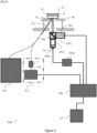
- FIG 1 illustrates a schematic view of a device Disp according to the invention for measuring in situ the lifetime of minority carriers in a semiconductor material, which may for example be a photovoltaic cell Ec by measuring a first photoluminescence signal PL1.
- This device is intended to implement the method of the figure 2 which we will detail later.
- the photovoltaic cell Ec made of semiconductor material comprises at least one first junction J1 comprising a layer absorbing incident light radiation having a forbidden band width or "gap" E g1 . Subsequently, it is considered that the terms junction and semiconductor layer absorbing incident radiation are equivalent.
- the cell photovoltaic cell is a single-junction cell.
- the photovoltaic cell is a cell comprising several junctions such as a multi-junction cell or a tandem cell (stack of two cells).
- the device Disp comprises a first laser source SL1 consisting of a laser L and a modulator PC.
- the laser L is a high-intensity monochromatic laser source.
- the laser is an LED or a SLED (Superluminescent Diode).
- the laser L comprises a high-intensity and broadband source coupled to a spectral filter.
- the modulator is an electronically controlled mechanical shutter.
- the modulator is an electronic modulator controlling the power supply of the laser.
- the first laser source is configured to emit a first light radiation (or excitation signal) L1 in at a first wavelength ⁇ 1 , configured to emit laser radiation at a plurality of distinct average intensities I1 i with iE[1,m]. Furthermore, via the modulator, the first laser source is configured to be modulated successively at a plurality of distinct modulation frequencies ⁇ j with j ⁇ [1,n].
- the first laser source is adapted to illuminate the first junction J1 of the photovoltaic cell Ec so as to generate a first photoluminescence signal PL1 in the first junction J1 of the photovoltaic cell.
- the first laser source SL1 is configured to emit laser radiation at a wavelength ⁇ 1 such that h / c ⁇ 1 > E g 1 in order to excite the photovoltaic cell.
- the PE sample holder is suitable for holding the photovoltaic cell fixed during its characterization during the manufacturing process in order to perform in-situ measurements.
- the sample holder is placed within a reactor during the annealing step of the photovoltaic cell, in order to follow the in-situ evolution of the photovoltaic cell during this step.
- the solar cell Once excited by the pulsed laser, the solar cell is in a state of disequilibrium.
- the solar cell returns to equilibrium by emitting light (luminescence of solar cells and more generally of semiconductor materials).
- the first light radiation excites the electrons in the valence band of the semiconductor (e.g. crystalline silicon), the latter being in the excited state in the conduction band.
- the first laser source SL1 emits a first light radiation at an average intensity I1 i with iE[1,m] modulated at a first modulation frequency ⁇ j with j ⁇ [1,n] and generating a first associated photoluminescence signal which we will call PL1 ij .
- the device of the figure 1 further comprises an optical collection system Col1 configured to collect the first photoluminescence signal PL1.
- this optical device consists of a parabolic mirror and a set of lenses for collimating the first photoluminescence signal and directing it onto a photodiode Phot for detecting the intensity of the first photoluminescence signal.
- this optical device consists of a set of achromatic doublets (lens doublets) for collimating the first photoluminescence signal.
- the first collected photoluminescence signal is coupled to an optical fiber and directed onto the photodiode.
- the first collected photoluminescence signal is focused directly onto the photodiode.
- the first laser source is configured so that the first light beam illuminates the first junction with an angle of incidence sufficient for the collection optical system not to collect the first light beam reflected by the photovoltaic cell.
- a high-pass filter is used to filter the reflection of the first laser source.
- the first laser source is configured so that the illuminated surface (i.e. photogeneration zone; typically a few millimeters in diameter) is larger than the collection surface (i.e. measurement zone; typically a few tens to a few hundreds of microns).
- the device comprises a pre-amplifier Amp configured to amplify the first photoluminescence signal after detection by the photodiode Phot.
- the device does not comprise an amplifier.
- the first photoluminescence signal is directed to a detection system Det connected to the first laser source SL1 and to a processing unit UT.
- the detection system comprises at least one synchronous detection amplifier (Lock-In Amplifier in English).
- FIG 2 illustrates a method for measuring in situ the lifetime of minority carriers in a photovoltaic cell according to the invention, implemented by the device of the figure 1 .
- This method comprises a first step A consisting of illuminating, by the first laser source SL1, at least the first junction J1 of the photovoltaic cell Ec with a first light radiation L1 in emitted at a plurality of average intensities I1 i , i ⁇ [1,m] and at a first wavelength ⁇ 1 adapted to generate a first photoluminescence signal PL1 in said first junction of the photovoltaic cell Ec.
- a step A2 consisting in modulating, by means of the modulator PC, the first light radiation emitted by the first laser source SL1 successively at a plurality n>1 of distinct modulation frequencies ⁇ j jE[1,n].
- the modulation frequencies are selected as a function of the first laser source SL1, the preamplifier and the lock-in amplifier. Typically, they are between 20 Hz and 100 kHz.
- the substep A21 is carried out consisting in detecting the amplitude, with the detection system Det, of the first photoluminescence signal PL1 ij associated with the first light radiation of average intensity I1 i and modulation frequency ⁇ j and measuring the phase shift ⁇ ij between the amplitude of the first incident light radiation and the amplitude of the first photoluminescence signal PL1.
- the measurement of the phase shift is for example carried out by the synchronous detection amplifier of the detection system, said synchronous detection amplifier being synchronized to the first laser source SL1.
- the method of the figure 2 comprises another step A3 consisting in calculating, using the processing unit Ut connected to the detection system, the minority carrier lifetime ⁇ i from the measurements of the phase shift ⁇ ij , with j ⁇ [1,n] between the intensity of the first incident light radiation and the intensity of the first photoluminescence signal.
- the minority carrier lifetime ⁇ i is therefore calculated, by the processing unit, from the slope of the line representing the value of the tangent of the phase shift tan( ⁇ ij ) as a function of the modulation frequency ⁇ j , this line drawn for all modulation frequencies ⁇ j , j ⁇ [1,n]. It is necessary to use a plurality of modulation frequencies in order to improve the reliability of the calculation of the lifetime. Preferably, at least 3 modulation frequencies are used.
- the method of the figure 2 allows to calculate a density ⁇ n i and a lifetime ⁇ i of minority charge carriers for each average intensity I1 i , i ⁇ [1,m] of the first light radiation. It is interesting to calculate the lifetime of the minority carriers for a plurality of distinct average intensities because, as we will explain later, this constitutes a necessary step for the determination of the lifetime for a specific reference carrier density. However, this determination is critical because the lifetime varies greatly depending on the density of minority carriers (variation can range from 100 to 1000 ⁇ s or more for crystalline silicon). This is the reason why, in the photovoltaic or electronic community, the lifetime of the minority carriers is presented for a specific carrier density (eg 10 15 cm -3 for a mono-junction solar cell in crystalline silicon).
- a specific carrier density eg 10 15 cm -3 for a mono-junction solar cell in crystalline silicon.
- the laser intensity is related to the photogeneration rate and also varies the carrier density. Therefore, it is very difficult to measure the carrier lifetime at a desired carrier density. It is therefore necessary to measure the carrier lifetime for several laser intensities in order to calculate the lifetime ⁇ at a desired density ⁇ n (eg 10 15 cm -3 ) by interpolation or extrapolation using the method of figure 3 detailed further below.
- the method of the figure 2 can be carried out in situ by the device of the figure 1 by repeating all of steps A-A4 several times during a photovoltaic cell treatment process in order to observe how the minority carrier lifetime evolves during the process.
- the method illustrated in the figure 2 requires a sufficiently long minority charge carrier lifetime.
- the first junction J1 is made of a material such that the minority charge carrier lifetime is greater than 1 ⁇ s, preferably greater than 10 ⁇ s.
- the first junction J1 is made of crystalline silicon (with a gap E g1 ) and the first laser source is configured to emit a first radiation at a first wavelength ⁇ 1 ⁇ hc / E g .
- FIG 3 illustrates a method for measuring in situ the lifetime of minority carriers in a photovoltaic cell according to a variant of the invention, implemented by the device of the figure 1 .
- This method is identical to that illustrated in the figure 2 except that it comprises three steps B, C and D carried out successively after steps A-A4 carried out for a plurality of average intensities I1 i , i ⁇ [1,m] of the first light radiation.
- Step B consists of the determination by the processing unit of a first continuous function f 1 calculating the minority carrier lifetime as a function of the minority carrier density from the values of the lifetime and the minority carrier density determined during step A4.
- This step therefore allows the determination of a function calculating the minority carrier lifetime for a specific reference carrier density.
- this continuous function allows us to have the correct parameters used for the correction of the lifetime calculation carried out in step C.
- Step C performed after step B, consists of calculating, with the processing unit, the minority carrier lifetime corrected from the derivative of the function f 1 , the calculation of the minority carrier lifetime and the photogeneration rate.
- the calculation of the minority carrier lifetime performed during step A3 is a so-called differential lifetime because the phase shift measurement technique is itself a dynamic measurement technique of the charge carrier recombination properties based on a relative variation in the illumination. That is to say, a global parameter of the photovoltaic cell is determined (the charge carrier lifetime ⁇ i for an average intensity I1 i ) by comparing measurements where only the frequency of modulation ⁇ j of the cell illumination varies.
- the method according to a first variant of the invention comprises a step D, after step C, of determination by the processing unit of a second continuous function f 2 calculating the corrected minority carrier lifetime as a function of the minority carrier density from the values of the corrected minority carrier lifetime ⁇ ci determined during step C.
- Step D allows the determination of a function calculating the corrected minority carrier lifetime for a specific carrier density.
- the lifetime calculated by the function f 2 is the corrected lifetime, the opposite of the lifetime calculated by the function f 1 which allows the differential lifetime to be calculated.
- the corrected lifetime is a standard lifetime used in the photovoltaic and microelectronics community to characterize the properties of a semiconductor material. According to an embodiment of this first variant of the invention, only step B is carried out, steps C and D being omitted.
- FIG 4 is a graph representing the first function f 1 (curve 31), determined during step B of the method of the first variant of the invention, calculating the evolution of the lifetime of minority carriers as a function of the density of minority carriers.
- the figure 4 further represents the second function f 2 (curve 32), determined during step D of the method of the first variant of the invention, calculating the evolution of the lifetime of minority carriers corrected as a function of the density of minority carriers.
- Curve 32 therefore makes it possible to determine the lifetime of minority charge carriers corrected for a specific carrier density.
- the number of distinct average intensities I1 i of the first light radiation is 6. This example is given for information purposes only. limiting and according to an embodiment of the first variation of the invention, a different number of 6 distinct average intensities is used when carrying out the method illustrated in figure 3 by the Disp device of the figure 1 .
- the laser intensities range from 2 mW to 50 mW and the modulation frequencies are between 225 Hz and 1025 Hz.
- the photovoltaic cell comprises at least two junctions, a first junction J1 with a gap E g1 and a second junction J2 with a gap E g2 > E g1 .
- the second junction of the photovoltaic cell can be made of a group III-V semiconductor material, perovskite or CIGS.
- the photovoltaic cell is a cell comprising at least two junctions such as a multi-junction cell or a tandem cell (stack of two cells).
- the device of the embodiment of the figure 5 is identical to that of the figure 1 except that it comprises a second laser source SL2 emitting a second light radiation L2in at a second wavelength ⁇ 2 at constant intensity.
- the second laser source is configured to illuminate the second junction J2 of the photovoltaic cell and to generate a second photoluminescence signal PL2 in said second junction of the photovoltaic cell.
- the second laser source SL2 is a high-intensity monochromatic laser source.
- the second laser source is an LED or an SLED.
- the first source and the second laser source are configured such that the second wavelength is less than the first wavelength ( ⁇ 2 ⁇ 1 ) and such that the second light radiation is completely absorbed by the second junction of the photovoltaic cell while the first light radiation passes through the second junction to be absorbed by the first junction.
- the device of the figure 5 further comprises an optical separator component Sep adapted to spatially separate the first signal from photoluminescence and the second photoluminescence signal from the photovoltaic cell.
- the optical separator component is a dichroic mirror.
- the detection system further comprises a photodetector configured to detect and measure the intensity of the second photoluminescence signal.
- the photodetector of the detection system is a photodiode or an avalanche photodiode.
- step A further comprises illuminating the second junction J2 of the photovoltaic cell with the second light radiation L2 in at a second wavelength adapted to generate a second photoluminescence signal PL2 in said second junction of the photovoltaic cell and step A21 further comprises detecting the second photoluminescence signal and measuring the intensity of the second photoluminescence signal.
- Measuring the intensity of the second photoluminescence signal makes it possible to trace the electrical properties of the second junction of the photovoltaic cell. In addition, this measurement is carried out simultaneously with the measurement of the phase shift between the amplitude of the first incident light radiation and the amplitude of the first photoluminescence signal PL1. Thus, it is possible to characterize simultaneously and independently the first junction and the second junction of the photovoltaic cell.
Landscapes
- Health & Medical Sciences (AREA)
- General Health & Medical Sciences (AREA)
- Life Sciences & Earth Sciences (AREA)
- Chemical & Material Sciences (AREA)
- Analytical Chemistry (AREA)
- Biochemistry (AREA)
- Physics & Mathematics (AREA)
- General Physics & Mathematics (AREA)
- Immunology (AREA)
- Pathology (AREA)
- Nuclear Medicine, Radiotherapy & Molecular Imaging (AREA)
- Testing Or Measuring Of Semiconductors Or The Like (AREA)
- Investigating, Analyzing Materials By Fluorescence Or Luminescence (AREA)
Claims (9)
- Verfahren zum In-situ-Messen der Lebensdauer von Minoritätsträgern in einem Halbleitermaterial (Ec), das mindestens einen ersten Übergang (J1) umfasst, durch Messen eines ersten Photolumineszenzsignals (PL1), wobei das Verfahren Folgendes umfasst:A. Beleuchten mindestens des ersten Übergangs (J1) des Halbleitermaterials (Ec) mit einer ersten Lichtstrahlung (L1in), die mit einer Vielzahl von durchschnittlichen Intensitäten I1i, i∈[1,m], und bei einer ersten Wellenlänge emittiert wird, die dazu ausgelegt ist, ein erstes Photolumineszenzsignal (PL1) in dem ersten Übergang des Halbleitermaterials zu erzeugen;
für jedes i∈[1,m] werden die Teilschritte ausgeführt, bestehend aus:A1 - Berechnen der Photogenerationsrate Gi der Ladungsträger;A2 - Modulieren der ersten Lichtstrahlung nacheinander mit einer Vielzahl n>1 unterschiedlicher Modulationsfrequenzen ωj, j∈[1,n], und für jedes j∈[1,n]:A21 - Erkennen des ersten Photolumineszenzsignals (PL1) und Messen der Phasenverschiebung Φij zwischen einer Amplitude der ersten einfallenden Lichtstrahlung (L1in) und einer Amplitude des ersten Photolumineszenzsignals (PL1)A3 - Berechnen der Lebensdauer der Minoritätsträger Ti aus Messungen der Phasenverschiebung Φij, mit je[1,n];A4 - Berechnen der Minoritätsträgerdichte Δni aus der Lebensdauer der Minoritätsträger Ti und der Photogenerationsrate GiB. Bestimmen, aus den in Schritt A4 bestimmten Werten, einer kontinuierlichen Funktion, die als erste Funktion bezeichnet wird, die die Entwicklung der Lebensdauer von Minoritätsträgern in Abhängigkeit von der Dichte der Minoritätsträger darstellt,C. Berechnen eines Werts der Lebensdauer der Minoritätsträger, korrigiert um die Vielzahl von durchschnittlichen Intensitäten, wobei die Berechnung aus der Ableitung der ersten Funktion, der Berechnung der Lebensdauer der Minoritätsträger und der Photogenerationsrate durchgeführt wird,D. Bestimmen, aus den in Schritt C bestimmten Werten der korrigierten Lebensdauer der Minoritätsträger, einer kontinuierlichen Funktion, die als zweite Funktion bezeichnet wird, durch Berechnen der korrigierten Lebensdauer der Minoritätsträger in Abhängigkeit von der Dichte der Minoritätsträger. - Verfahren nach dem vorstehenden Anspruch, wobei das Halbleitermaterial ferner einen zweiten Übergang (J2) mit einer Bandlückenbreite umfasst, die größer als die Breite der Bandlücke des ersten Übergangs ist, und wobei:- Schritt A ferner das Beleuchten des zweiten Übergangs mit einer zweiten Lichtstrahlung (L2in) bei einer zweiten Wellenlänge umfasst, die dazu ausgelegt ist, ein zweites Photolumineszenzsignal (PL2) in dem zweiten Übergang des Halbleitermaterials zu erzeugen;- Schritt A21 ferner das Erkennen des zweiten Photolumineszenzsignals und das Messen der Intensität des zweiten Photolumineszenzsignals umfasst.
- Verfahren nach dem vorstehenden Anspruch, wobei während der Beleuchtung die zweite Wellenlänge kleiner als die erste Wellenlänge ist und die zweite Lichtstrahlung vom zweiten Übergang des Halbleitermaterials absorbiert wird, während die erste Lichtstrahlung den zweiten Übergang durchquert, um vom ersten Übergang absorbiert zu werden.
- Verfahren nach einem der vorstehenden Ansprüche, wobei mindestens die Schritte A bis A4 während eines Verarbeitungsprozesses des Halbleitermaterials mehrmals wiederholt werden.
- Vorrichtung (Disp) zum In-situ-Messen der Lebensdauer von Minoritätsträgern in einem Halbleitermaterial (Ec), das mindestens einen ersten Übergang (J1) umfasst, durch Messung eines ersten Photolumineszenzsignals (PL1), wobei die Vorrichtung Folgendes umfasst:- mindestens eine erste Laserquelle (SL1), die eine erste Lichtstrahlung (L1in) mit einer ersten Wellenlänge emittiert, die konfiguriert ist, um Laserstrahlung mit einer Vielzahl von unterschiedlichen durchschnittlichen Intensitäten I1i mit i∈[1,m] zu emittieren und konfiguriert ist, um nacheinander mit einer Vielzahl von unterschiedlichen Modulationsfrequenzen ωj mit j∈[1,n] moduliert zu werden und konfiguriert ist, um einen ersten Übergang des Halbleitermaterials zu beleuchten, um so ein erstes Photolumineszenzsignal (PL1) in dem ersten Übergang (J1) des Halbleitermaterials zu erzeugen;- ein Detektionssystem (Det), das mit der ersten Laserquelle (SL1) verbunden ist und dazu ausgelegt ist, das erste Photolumineszenzsignal (PL1) zu erkennen und Phasenverschiebungen Φij, zwischen der Amplitude jeder ersten einfallenden Lichtstrahlung (L1in) der Intensität I1i und der Modulationsfrequenz ωj und der Amplitude des zugehörigen ersten Photolumineszenzsignals (PL1) zu messen;- eine Verarbeitungseinheit (UT), die mit dem Detektionssystem verbunden ist und für Folgendes ausgelegt ist:- Berechnen, für jede unterschiedliche durchschnittliche Intensität I1i der ersten Lichtstrahlung, der Photogenerationsrate Gi der Minoritätsladungsträger;- Berechnen, für jede unterschiedliche durchschnittliche Intensität I1i der ersten Lichtstrahlung, der Lebensdauer der Minoritätsträger Ti aus Messungen der Phasenverschiebung Φij;- Berechnen, für jede unterschiedliche durchschnittliche Intensität I1i der ersten Lichtstrahlung, der Dichte der Minoritätsträger Δni aus der Lebensdauer der Minoritätsträger Ti und der Photogenerationsrate Gi,- Anpassen einer kontinuierlichen Funktion, die als erste Funktion bezeichnet wird, durch Berechnen der Lebensdauer der Minoritätsträger in Abhängigkeit von der Dichte der Minoritätsträger für die Vielzahl unterschiedlicher durchschnittlicher Intensitäten der ersten Lichtstrahlung- Berechnen der Werte der korrigierten Lebensdauer der Minoritätsträger, wobei die Berechnung aus der Ableitung der ersten Funktion, der Berechnung der Lebensdauer der Minoritätsträger und der Photogenerationsrate durchgeführt wird,- Bestimmen, aus den berechneten Werten der korrigierten Lebensdauer der Minoritätsträger, einer kontinuierlichen Funktion, die als zweite Funktion bezeichnet wird, durch Berechnen der korrigierten Lebensdauer der Minoritätsträger in Abhängigkeit von der Dichte der Minoritätsträger.
- Vorrichtung nach Anspruch 5, wobei das Detektionssystem mindestens einen synchronen Detektionsverstärker umfasst.
- Vorrichtung nach einem der zwei vorstehenden Ansprüche, umfassend:- eine zweite Laserquelle (SL2), die eine zweite Lichtstrahlung (L2in) bei einer zweiten Wellenlänge emittiert, wobei die zweite Laserquelle konfiguriert ist, um einen zweiten Übergang (J2) des Halbleitermaterials mit einer Bandlückenbreite zu beleuchten, die größer als die Breite der Bandlücke des ersten Übergangs ist, und um ein zweites Photolumineszenzsignal (PL2) in dem zweiten Übergang des Halbleitermaterials zu erzeugen,- eine optische Trennkomponente (Sep), die dazu ausgelegt ist, das erste Photolumineszenzsignal und das zweite Photolumineszenzsignal räumlich zu trennen; wobei das Detektionssystem ferner konfiguriert ist, um das zweite Photolumineszenzsignal zu erkennen und die Intensität des zweiten Photolumineszenzsignals zu messen.
- Vorrichtung nach dem vorstehenden Anspruch, wobei die erste Laserquelle und die zweite Laserquelle so konfiguriert sind, dass die zweite Wellenlänge kleiner als die erste Wellenlänge ist und die zweite Lichtstrahlung von dem zweiten Übergang des Halbleitermaterials absorbiert wird, während die erste Lichtstrahlung den zweiten Übergang durchquert, um vom ersten Übergang absorbiert zu werden.
- Vorrichtung nach einem der zwei vorstehenden Ansprüche, wobei das Detektionssystem mindestens einen Photodetektor umfasst.
Applications Claiming Priority (1)
| Application Number | Priority Date | Filing Date | Title |
|---|---|---|---|
| FR1908051A FR3098913B1 (fr) | 2019-07-17 | 2019-07-17 | Dispositif et méthode pour mesurer in-situ le temps de vie de porteurs minoritaires dans un matériau semi-conducteur |
Publications (2)
| Publication Number | Publication Date |
|---|---|
| EP3767282A1 EP3767282A1 (de) | 2021-01-20 |
| EP3767282B1 true EP3767282B1 (de) | 2025-02-12 |
Family
ID=68138530
Family Applications (1)
| Application Number | Title | Priority Date | Filing Date |
|---|---|---|---|
| EP20185506.1A Active EP3767282B1 (de) | 2019-07-17 | 2020-07-13 | Vorrichtung und methode zur in-situ-messung der lebensdauer von minoritätsträgern in einem halbleitermaterial |
Country Status (3)
| Country | Link |
|---|---|
| EP (1) | EP3767282B1 (de) |
| ES (1) | ES3025510T3 (de) |
| FR (1) | FR3098913B1 (de) |
Families Citing this family (2)
| Publication number | Priority date | Publication date | Assignee | Title |
|---|---|---|---|---|
| EP4257958A1 (de) * | 2022-04-05 | 2023-10-11 | Centre national de la recherche scientifique | Verfahren und vorrichtung zur bestimmung der effektiven elektronenlebensdauer in einer probe |
| EP4556891A1 (de) | 2023-11-16 | 2025-05-21 | Centre National de la Recherche Scientifique | Verfahren und vorrichtung zur vereinfachten bestimmung der effektiven elektronenlebensdauer |
Family Cites Families (4)
| Publication number | Priority date | Publication date | Assignee | Title |
|---|---|---|---|---|
| EP2319073A1 (de) * | 2008-07-09 | 2011-05-11 | BT Imaging Pty Ltd | Dünnfilmbildgebungsverfahren und vorrichtung |
| TW201140039A (en) * | 2010-01-04 | 2011-11-16 | Bt Imaging Pty Ltd | Improved illumination systems and methods for photoluminescence imaging of photovoltaic cells and wafers |
| DE102010019132A1 (de) * | 2010-04-30 | 2011-11-03 | Fraunhofer-Gesellschaft zur Förderung der angewandten Forschung e.V. | Verfahren zur Bestimmung von Materialparametern eines dotierten Halbleitersubstrates durch Messung von Photolumineszenzstrahlung |
| US9075012B2 (en) | 2011-11-10 | 2015-07-07 | Alliance For Sustainable Energy, Llc | Photoluminescence-based quality control for thin film absorber layers of photovoltaic devices |
-
2019
- 2019-07-17 FR FR1908051A patent/FR3098913B1/fr active Active
-
2020
- 2020-07-13 EP EP20185506.1A patent/EP3767282B1/de active Active
- 2020-07-13 ES ES20185506T patent/ES3025510T3/es active Active
Also Published As
| Publication number | Publication date |
|---|---|
| FR3098913B1 (fr) | 2021-08-06 |
| ES3025510T3 (en) | 2025-06-09 |
| EP3767282A1 (de) | 2021-01-20 |
| FR3098913A1 (fr) | 2021-01-22 |
Similar Documents
| Publication | Publication Date | Title |
|---|---|---|
| EP3298390B1 (de) | Mikrophotolumineszenzbildgebung mit optischer filtrierung | |
| EP2880426B1 (de) | Verfahren zur analyse der kristallstruktur eines polykristallinen halbleiters | |
| EP3084402B1 (de) | Verfahren zur überwachung der qualität von photovoltaikzellen | |
| EP3767282B1 (de) | Vorrichtung und methode zur in-situ-messung der lebensdauer von minoritätsträgern in einem halbleitermaterial | |
| EP3436807B1 (de) | Verfahren und system zur inspektion von platten für die mikroelektronik oder optik durch laser-doppler-effekt | |
| EP3599717B1 (de) | Optische characterisierung eines koeffizientes von beidseitigkeit eines beidseitigen solamoduls | |
| EP3407055A1 (de) | Quantitative spektroskopie der dichte von elektronischen fehlern in einem in eine dünnschicht integrierten foto-rezeptor, insbesondere in einer solarzelle | |
| EP2932236B1 (de) | Lichtrefklektierende vorrichtung | |
| FR2956208A1 (fr) | Methode de determination sans contact de caracteristiques d'un photoconvertisseur | |
| EP3447909B1 (de) | Verfahren und vorrichtung zur charakterisierung eines fotovoltaikmoduls | |
| EP3413035B1 (de) | Verfahren zur bestimmung von abfallzeiten eines lumineszenzsignals | |
| EP3789759B1 (de) | Elektrolumineszenz-kartierung von verunreinigungen in vorrichtungen mit halbleitermaterialien | |
| US20230282526A1 (en) | Method and device for measuring the thickness of thin films even on rough substrates | |
| Johnston et al. | Photoluminescence imaging characterization of thin-film InP | |
| EP4174474A1 (de) | Verfahren zur bestimmung der position mindestens eines defekts auf halbleitersubstraten, nachweisverfahren und vorrichtung dafür | |
| BE1019539A3 (fr) | Methode de determination de la transmission opto-energetique d'un materiau transparent ou translucide et dispositif pour sa mise en oeuvre. | |
| WO2025056736A1 (fr) | Procédé et dispositif électronique de détermination d'un paramètre électrique d'une cellule photovoltaïque tandem, programme d'ordinateur et système de caractérisation associés | |
| WO2001065596A2 (fr) | Procede de controle de l'uniformite de traitement d'une surface de materiau pour la microelectronique par un faisceau de particules electriquement chargees et equipement de mise en oeuvre | |
| EP4012786A1 (de) | Verfahren zur bestimmung einer heiztemperatur von einer heteroübergangs-photovoltaikzelle in einem verarbeitungsverfahren | |
| EP3835756A1 (de) | Vorrichtung und verfahren zur partikeldetektion und verfahren zur herstellung |
Legal Events
| Date | Code | Title | Description |
|---|---|---|---|
| PUAI | Public reference made under article 153(3) epc to a published international application that has entered the european phase |
Free format text: ORIGINAL CODE: 0009012 |
|
| STAA | Information on the status of an ep patent application or granted ep patent |
Free format text: STATUS: THE APPLICATION HAS BEEN PUBLISHED |
|
| AK | Designated contracting states |
Kind code of ref document: A1 Designated state(s): AL AT BE BG CH CY CZ DE DK EE ES FI FR GB GR HR HU IE IS IT LI LT LU LV MC MK MT NL NO PL PT RO RS SE SI SK SM TR |
|
| AX | Request for extension of the european patent |
Extension state: BA ME |
|
| STAA | Information on the status of an ep patent application or granted ep patent |
Free format text: STATUS: REQUEST FOR EXAMINATION WAS MADE |
|
| 17P | Request for examination filed |
Effective date: 20210713 |
|
| RBV | Designated contracting states (corrected) |
Designated state(s): AL AT BE BG CH CY CZ DE DK EE ES FI FR GB GR HR HU IE IS IT LI LT LU LV MC MK MT NL NO PL PT RO RS SE SI SK SM TR |
|
| RAP1 | Party data changed (applicant data changed or rights of an application transferred) |
Owner name: TOTALENERGIES ONETECH Owner name: ECOLE POLYTECHNIQUE Owner name: ELECTRICITE DE FRANCE Owner name: INSTITUT PHOTOVOLTAIQUE D'ILE DE FRANCE - IPVF Owner name: CENTRE NATIONAL DE LA RECHERCHE SCIENTIFIQUE |
|
| STAA | Information on the status of an ep patent application or granted ep patent |
Free format text: STATUS: EXAMINATION IS IN PROGRESS |
|
| 17Q | First examination report despatched |
Effective date: 20221212 |
|
| GRAP | Despatch of communication of intention to grant a patent |
Free format text: ORIGINAL CODE: EPIDOSNIGR1 |
|
| STAA | Information on the status of an ep patent application or granted ep patent |
Free format text: STATUS: GRANT OF PATENT IS INTENDED |
|
| INTG | Intention to grant announced |
Effective date: 20240912 |
|
| GRAS | Grant fee paid |
Free format text: ORIGINAL CODE: EPIDOSNIGR3 |
|
| GRAA | (expected) grant |
Free format text: ORIGINAL CODE: 0009210 |
|
| STAA | Information on the status of an ep patent application or granted ep patent |
Free format text: STATUS: THE PATENT HAS BEEN GRANTED |
|
| AK | Designated contracting states |
Kind code of ref document: B1 Designated state(s): AL AT BE BG CH CY CZ DE DK EE ES FI FR GB GR HR HU IE IS IT LI LT LU LV MC MK MT NL NO PL PT RO RS SE SI SK SM TR |
|
| REG | Reference to a national code |
Ref country code: GB Ref legal event code: FG4D Free format text: NOT ENGLISH |
|
| REG | Reference to a national code |
Ref country code: CH Ref legal event code: EP |
|
| REG | Reference to a national code |
Ref country code: DE Ref legal event code: R096 Ref document number: 602020045816 Country of ref document: DE |
|
| REG | Reference to a national code |
Ref country code: IE Ref legal event code: FG4D Free format text: LANGUAGE OF EP DOCUMENT: FRENCH |
|
| REG | Reference to a national code |
Ref country code: ES Ref legal event code: FG2A Ref document number: 3025510 Country of ref document: ES Kind code of ref document: T3 Effective date: 20250609 |
|
| REG | Reference to a national code |
Ref country code: NL Ref legal event code: MP Effective date: 20250212 |
|
| PG25 | Lapsed in a contracting state [announced via postgrant information from national office to epo] |
Ref country code: RS Free format text: LAPSE BECAUSE OF FAILURE TO SUBMIT A TRANSLATION OF THE DESCRIPTION OR TO PAY THE FEE WITHIN THE PRESCRIBED TIME-LIMIT Effective date: 20250512 |
|
| PG25 | Lapsed in a contracting state [announced via postgrant information from national office to epo] |
Ref country code: FI Free format text: LAPSE BECAUSE OF FAILURE TO SUBMIT A TRANSLATION OF THE DESCRIPTION OR TO PAY THE FEE WITHIN THE PRESCRIBED TIME-LIMIT Effective date: 20250212 |
|
| PG25 | Lapsed in a contracting state [announced via postgrant information from national office to epo] |
Ref country code: PL Free format text: LAPSE BECAUSE OF FAILURE TO SUBMIT A TRANSLATION OF THE DESCRIPTION OR TO PAY THE FEE WITHIN THE PRESCRIBED TIME-LIMIT Effective date: 20250212 |
|
| REG | Reference to a national code |
Ref country code: LT Ref legal event code: MG9D |
|
| PG25 | Lapsed in a contracting state [announced via postgrant information from national office to epo] |
Ref country code: IS Free format text: LAPSE BECAUSE OF FAILURE TO SUBMIT A TRANSLATION OF THE DESCRIPTION OR TO PAY THE FEE WITHIN THE PRESCRIBED TIME-LIMIT Effective date: 20250612 Ref country code: NO Free format text: LAPSE BECAUSE OF FAILURE TO SUBMIT A TRANSLATION OF THE DESCRIPTION OR TO PAY THE FEE WITHIN THE PRESCRIBED TIME-LIMIT Effective date: 20250512 |
|
| PG25 | Lapsed in a contracting state [announced via postgrant information from national office to epo] |
Ref country code: NL Free format text: LAPSE BECAUSE OF FAILURE TO SUBMIT A TRANSLATION OF THE DESCRIPTION OR TO PAY THE FEE WITHIN THE PRESCRIBED TIME-LIMIT Effective date: 20250212 |
|
| PG25 | Lapsed in a contracting state [announced via postgrant information from national office to epo] |
Ref country code: HR Free format text: LAPSE BECAUSE OF FAILURE TO SUBMIT A TRANSLATION OF THE DESCRIPTION OR TO PAY THE FEE WITHIN THE PRESCRIBED TIME-LIMIT Effective date: 20250212 |
|
| PG25 | Lapsed in a contracting state [announced via postgrant information from national office to epo] |
Ref country code: LV Free format text: LAPSE BECAUSE OF FAILURE TO SUBMIT A TRANSLATION OF THE DESCRIPTION OR TO PAY THE FEE WITHIN THE PRESCRIBED TIME-LIMIT Effective date: 20250212 Ref country code: PT Free format text: LAPSE BECAUSE OF FAILURE TO SUBMIT A TRANSLATION OF THE DESCRIPTION OR TO PAY THE FEE WITHIN THE PRESCRIBED TIME-LIMIT Effective date: 20250612 |
|
| PG25 | Lapsed in a contracting state [announced via postgrant information from national office to epo] |
Ref country code: BG Free format text: LAPSE BECAUSE OF FAILURE TO SUBMIT A TRANSLATION OF THE DESCRIPTION OR TO PAY THE FEE WITHIN THE PRESCRIBED TIME-LIMIT Effective date: 20250212 Ref country code: GR Free format text: LAPSE BECAUSE OF FAILURE TO SUBMIT A TRANSLATION OF THE DESCRIPTION OR TO PAY THE FEE WITHIN THE PRESCRIBED TIME-LIMIT Effective date: 20250513 |
|
| REG | Reference to a national code |
Ref country code: AT Ref legal event code: MK05 Ref document number: 1766450 Country of ref document: AT Kind code of ref document: T Effective date: 20250212 |
|
| PG25 | Lapsed in a contracting state [announced via postgrant information from national office to epo] |
Ref country code: SE Free format text: LAPSE BECAUSE OF FAILURE TO SUBMIT A TRANSLATION OF THE DESCRIPTION OR TO PAY THE FEE WITHIN THE PRESCRIBED TIME-LIMIT Effective date: 20250212 |
|
| PG25 | Lapsed in a contracting state [announced via postgrant information from national office to epo] |
Ref country code: SM Free format text: LAPSE BECAUSE OF FAILURE TO SUBMIT A TRANSLATION OF THE DESCRIPTION OR TO PAY THE FEE WITHIN THE PRESCRIBED TIME-LIMIT Effective date: 20250212 |
|
| PGFP | Annual fee paid to national office [announced via postgrant information from national office to epo] |
Ref country code: ES Payment date: 20250929 Year of fee payment: 6 |
|
| PG25 | Lapsed in a contracting state [announced via postgrant information from national office to epo] |
Ref country code: DK Free format text: LAPSE BECAUSE OF FAILURE TO SUBMIT A TRANSLATION OF THE DESCRIPTION OR TO PAY THE FEE WITHIN THE PRESCRIBED TIME-LIMIT Effective date: 20250212 |
|
| PGFP | Annual fee paid to national office [announced via postgrant information from national office to epo] |
Ref country code: DE Payment date: 20250825 Year of fee payment: 6 |
|
| PGFP | Annual fee paid to national office [announced via postgrant information from national office to epo] |
Ref country code: IT Payment date: 20250725 Year of fee payment: 6 |
|
| PG25 | Lapsed in a contracting state [announced via postgrant information from national office to epo] |
Ref country code: AT Free format text: LAPSE BECAUSE OF FAILURE TO SUBMIT A TRANSLATION OF THE DESCRIPTION OR TO PAY THE FEE WITHIN THE PRESCRIBED TIME-LIMIT Effective date: 20250212 |
|
| PGFP | Annual fee paid to national office [announced via postgrant information from national office to epo] |
Ref country code: FR Payment date: 20250729 Year of fee payment: 6 |
|
| PG25 | Lapsed in a contracting state [announced via postgrant information from national office to epo] |
Ref country code: EE Free format text: LAPSE BECAUSE OF FAILURE TO SUBMIT A TRANSLATION OF THE DESCRIPTION OR TO PAY THE FEE WITHIN THE PRESCRIBED TIME-LIMIT Effective date: 20250212 Ref country code: CZ Free format text: LAPSE BECAUSE OF FAILURE TO SUBMIT A TRANSLATION OF THE DESCRIPTION OR TO PAY THE FEE WITHIN THE PRESCRIBED TIME-LIMIT Effective date: 20250212 |
|
| PG25 | Lapsed in a contracting state [announced via postgrant information from national office to epo] |
Ref country code: RO Free format text: LAPSE BECAUSE OF FAILURE TO SUBMIT A TRANSLATION OF THE DESCRIPTION OR TO PAY THE FEE WITHIN THE PRESCRIBED TIME-LIMIT Effective date: 20250212 |
|
| PG25 | Lapsed in a contracting state [announced via postgrant information from national office to epo] |
Ref country code: SK Free format text: LAPSE BECAUSE OF FAILURE TO SUBMIT A TRANSLATION OF THE DESCRIPTION OR TO PAY THE FEE WITHIN THE PRESCRIBED TIME-LIMIT Effective date: 20250212 |
|
| REG | Reference to a national code |
Ref country code: DE Ref legal event code: R097 Ref document number: 602020045816 Country of ref document: DE |
|
| PLBE | No opposition filed within time limit |
Free format text: ORIGINAL CODE: 0009261 |
|
| STAA | Information on the status of an ep patent application or granted ep patent |
Free format text: STATUS: NO OPPOSITION FILED WITHIN TIME LIMIT |
|
| REG | Reference to a national code |
Ref country code: CH Ref legal event code: L10 Free format text: ST27 STATUS EVENT CODE: U-0-0-L10-L00 (AS PROVIDED BY THE NATIONAL OFFICE) Effective date: 20251224 |
|
| 26N | No opposition filed |
Effective date: 20251113 |
|
| REG | Reference to a national code |
Ref country code: CH Ref legal event code: H13 Free format text: ST27 STATUS EVENT CODE: U-0-0-H10-H13 (AS PROVIDED BY THE NATIONAL OFFICE) Effective date: 20260224 |
|
| PG25 | Lapsed in a contracting state [announced via postgrant information from national office to epo] |
Ref country code: LU Free format text: LAPSE BECAUSE OF NON-PAYMENT OF DUE FEES Effective date: 20250713 |
|
| GBPC | Gb: european patent ceased through non-payment of renewal fee |
Effective date: 20250713 |
|
| REG | Reference to a national code |
Ref country code: BE Ref legal event code: MM Effective date: 20250731 |
|
| PG25 | Lapsed in a contracting state [announced via postgrant information from national office to epo] |
Ref country code: GB Free format text: LAPSE BECAUSE OF NON-PAYMENT OF DUE FEES Effective date: 20250713 |
|
| PG25 | Lapsed in a contracting state [announced via postgrant information from national office to epo] |
Ref country code: BE Free format text: LAPSE BECAUSE OF NON-PAYMENT OF DUE FEES Effective date: 20250731 |
|
| PG25 | Lapsed in a contracting state [announced via postgrant information from national office to epo] |
Ref country code: CH Free format text: LAPSE BECAUSE OF NON-PAYMENT OF DUE FEES Effective date: 20250731 |