EP3766665A1 - Device for applying a protective film on a screen of an electronic apparatus - Google Patents
Device for applying a protective film on a screen of an electronic apparatus Download PDFInfo
- Publication number
- EP3766665A1 EP3766665A1 EP20186288.5A EP20186288A EP3766665A1 EP 3766665 A1 EP3766665 A1 EP 3766665A1 EP 20186288 A EP20186288 A EP 20186288A EP 3766665 A1 EP3766665 A1 EP 3766665A1
- Authority
- EP
- European Patent Office
- Prior art keywords
- edge portion
- screen
- support base
- film
- laminar element
- Prior art date
- Legal status (The legal status is an assumption and is not a legal conclusion. Google has not performed a legal analysis and makes no representation as to the accuracy of the status listed.)
- Granted
Links
Images


Classifications
-
- B—PERFORMING OPERATIONS; TRANSPORTING
- B29—WORKING OF PLASTICS; WORKING OF SUBSTANCES IN A PLASTIC STATE IN GENERAL
- B29C—SHAPING OR JOINING OF PLASTICS; SHAPING OF MATERIAL IN A PLASTIC STATE, NOT OTHERWISE PROVIDED FOR; AFTER-TREATMENT OF THE SHAPED PRODUCTS, e.g. REPAIRING
- B29C63/00—Lining or sheathing, i.e. applying preformed layers or sheathings of plastics; Apparatus therefor
- B29C63/02—Lining or sheathing, i.e. applying preformed layers or sheathings of plastics; Apparatus therefor using sheet or web-like material
-
- B—PERFORMING OPERATIONS; TRANSPORTING
- B29—WORKING OF PLASTICS; WORKING OF SUBSTANCES IN A PLASTIC STATE IN GENERAL
- B29C—SHAPING OR JOINING OF PLASTICS; SHAPING OF MATERIAL IN A PLASTIC STATE, NOT OTHERWISE PROVIDED FOR; AFTER-TREATMENT OF THE SHAPED PRODUCTS, e.g. REPAIRING
- B29C63/00—Lining or sheathing, i.e. applying preformed layers or sheathings of plastics; Apparatus therefor
- B29C63/0004—Component parts, details or accessories; Auxiliary operations
- B29C2063/0008—Registering, centering the lining material on the substrate
Definitions
- the present invention is related to the technical field of the accessories for electronic devices, and more specifically it concerns a device for applying a protective film to the screen of an electronic apparatus such as, for example, a smartphone, a tablet or a similar apparatus.
- the screens of mobile electronic devices such as, for example, smartphones, tablets, industrial readers and similar devices are made of glass-based composite materials and can be damaged or even break if their external surface is rubbed against hard objects or is subjected to hard impacts.
- These films have their lower surface covered with adhesive and intended to be superimposed to the external surface of the screen.
- the main drawback that occurs during the manual application of the film to the screen of the device is represented by the need to position the film correctly, aligning its edges with those of the screen.
- the user often needs to position the film on the screen several times and this may reduce the bonding power of the glue or increase the risk of fingerprints or marks being left on the surface of the screen or of the film.
- Document WO2015/021430 describes a method and a device for applying a protective film to the screen of an electronic apparatus, which comprises a polygonal base provided with a seat for housing the electronic apparatus.
- the protective film has its underside covered with glue and provided with a flexible tab made of a polymeric material and folded on itself which respectively has a lower brush and an end projecting from the upper edge of the film.
- the upper surface of the film is covered with a further protective layer on which a laminar projection has been applied, said laminar projection being provided with two holes suited to allow the insertion of two holes formed on the base in proximity to the seat.
- a first drawback of this solution lies in that the insertion of the pins in the holes formed in the projection considerably slows down the operations required for the application of the protective film to the screen of the electronic apparatus.
- the operator must insert the pins formed on the base in the holes made in the film or in the laminar tab and must also check that the latter does not come off the pins during the application of the film.
- the present invention intends to overcome the drawbacks mentioned above by providing a device for applying a protective film to the screen of an electronic apparatus, wherein said device is particularly effective and flexible during use.
- the subject of the present invention is a device for applying a protective film P to the screen S of an electronic apparatus A.
- Said device can be particularly suited to allow a protective film P to be applied to the screen S of a smartphone, a tablet, a convertible notebook, an e-book reader and of all similar electronic apparatuses A.
- said device 1 can be configured to apply a protective film P to the screen S of the electronic apparatus A, wherein said protective film P can be of the flexible or rigid type, according to the preferences of the user of the device or of the owner of the apparatus. Furthermore, the film P can be completely transparent or of the semi-transparent type.
- the protective film P has an upper surface P' and a lower surface P" to which an adhesive layer J is applied, said adhesive layer J being suited to allow the lower surface P" to adhere to the external surface S' of the screen S.
- the adhesive layer J can cover the lower surface P" of the film P completely or can be distributed only on a portion (or on several portions) of the same.
- the device comprises a support base 2 provided with at least one housing 3 for the positioning of the electronic apparatus A.
- the support base 2 can have a substantially polygonal shape and on the same it will be possible to obtain a housing 3 in a substantially rectangular shape, which is suited to allow the precise positioning of the electronic apparatus A, that is, to allow the latter to be positioned with a reduced play.
- the relatively precise positioning of the electronic apparatus A in the housing 3 makes it possible to define a fixed and stable position of the apparatus A with respect to the other components of the device 1 which are used during the operations required for the application of the film P.
- the support base 2 has a housing 3 with fixed dimensions.
- the housing 3 can have variable dimensions in order to allow electronic apparatuses of different sizes to be positioned therein, wherein the length and width of said apparatuses can vary between a minimum and a maximum predetermined value.
- one or more terminal edges 4, 5 of the housing (for example, the edge 4 associated with the length of the electronic apparatus, or the edge 5 associated with its width, or both edges 4, 5) can be movable with respect to the support base 2 between two predetermined terminal positions suited to define, respectively, the minimum and the maximum dimension of the apparatus A that allow the latter to be inserted in the housing 3.
- the support base 2 furthermore comprises at least one edge portion 6 extending on the periphery of the housing 3.
- edge portion 6 formed on the base 2 defines at least one terminal edge 4, 5 which delimits the housing 3.
- edge portions 6 arranged peripherally on all sides of the housing 3.
- the latter is delimited by four terminal edges 4, 5 suited to delimit both the corresponding edge portion 6 (four of these being present) and the housing 3.
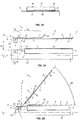
- the device 1 comprises a flexible laminar element 7, better illustrated in Figures 2A and 2B , provided with an upper surface 8 and a lower surface 9.
- the shape of the laminar element 7 in a plan view can be substantially considered as a rectangle to which one pair of terminal projections 10, 11 has been applied.
- the lower surface 9 of the laminar element 7 has a first portion 12 at least partially covered with an adhesive layer 13 and intended to be superimposed to the upper surface P" of the film P in such a way as to form with the latter a unit assembly indicated by the reference number 14 in Figure 1 and in Figure 3A .
- the lower surface 9 of the flexible laminar element 7 has also a second portion 16 arranged beside the first portion 12.
- the first portion 12 of the lower surface 9 has a rather large extension, as it occupies almost the entirety of the area enclosed by the rectangular shape that defines the main part of the laminar element 7.
- the upper projection 10 does not belong to the first portion 12 and therefore no adhesive is applied to the same. In this way, said projection 10 can be easily grasped by the user to remove the flexible laminar element 7 from the protective film P following the application of the latter to the screen S of the apparatus.
- Means 16 are also provided, which are suited to promote the removable coupling of the unit assembly 14 with the edge portion 6 of the support base.
- This coupling is suited to allow the protective film P to rotate around a predetermined hinge axis X.
- the support base has a longitudinal development axis L and the hinge axis X lies substantially crosswise with respect to said development axis L.
- the development axis L will be arranged in a substantially horizontal position and therefore the hinge axis X will be substantially parallel to the vertical.
- the peculiar characteristic of the coupling means 16 lies in that they promote the selective and removable coupling of the second portion 15 of the flexible laminar element 7 with the edge portion 6 formed on the base 2.
- Figure 3B illustrates the position of the protective film P before its application to the screen S of the electronic apparatus A.
- the coupling means 16 are configured to allow the assembly 14 (and in particular the film P) to selectively rotate around the hinge axis X between an initial position, in which the film P is not in contact with the screen S, and a final position, in which the adhesive layer J distributed on the lower surface P" of the film P is in contact with the upper surface S' of the screen S.
- Figure 3A shows the film P in the initial position
- Figure 3B shows the film P in the final position
- the coupling means 16 are able to promote the rotation of the assembly 14 around the hinge axis X over an angular amplitude ⁇ smaller than a straight angle (and typically close to a right angle); it is evident that this angular amplitude ⁇ is delimited by the initial and final position of the film P.
- the coupling means 16 comprise at least one magnetic element 17 associated with the second portion 15 of the flexible laminar element 7 and/or with the corresponding edge portion 6 formed on the support base 2.
- the magnetic element 17 is constituted by a substantially laminar metallic plate 18 that completely covers the second portion 15 of the lower surface 9 of the flexible laminar element 7.
- This plate 18 can be a permanent magnet or an element obtained from a permanent magnetic material such as, for example, neodymium or other rare-earth elements similar to it.
- the second portion 15 is covered by a thin adhesive layer 19 suited to promote the stable coupling of the magnetic element 18, that is, of the metallic plate 19, with the lower surface 9 of the flexible laminar element 7.
- the magnetic plate 18 is configured to interact with the corresponding edge portion 6 in such a way as to removably hold the unit assembly 14 on the base 2.
- the area of the edge portion 6 designed to be coupled with the magnetic plate 18 is made of a ferromagnetic material.
- an attraction force F is generated which acts on the plate 18 and is directed towards the base 2; said force F, illustrated in Figure 3A , causes the components 18, 2 to move towards each other until they come in contact with each other.
- the magnetic force F that maintains the plate 18 in contact with the base 2 thus makes it possible to maintain the base 2 substantially coupled with the unit assembly 14 in a removable manner.
- the entire edge portion 6 or the entire support base 2 from a ferromagnetic material (ferrous alloys, steel, etc).
- the protective film P is free to selectively rotate around the hinge axis X between its initial position and its final position, as better illustrated in Figures 3A and 3B .
- the edge portion 6 can be provided with a shaped recess, indicated by the reference number 20 in the figures, which is positioned in proximity to the area where it interacts with the second portion 15 of the lower surface 9 of the flexible laminar element 7.
- the dimensions l 1 , w 1 of said recess 20 are selected in such a way that they are substantially the same as the dimensions l 2 , w 2 of the magnetic element 17, that is, as the dimensions of the plate 18.
- the magnetic plate 18 comes to be positioned inside the recess 20, so that the upper surface 8 of the flexible laminar element 7 is substantially flush with (or slightly above) the upper surface 22 of the edge portion 6.
- the magnetic plate 18 can be inserted in the recess 20 with a relatively reduced play, in such a way as to define a fixed reference position of the unit assembly 14 with respect to the housing 3.
- said magnetic elements 17 are positioned in the edge portion 6 in proximity to the area where the latter interacts with the second portion 15 of the flexible laminar element 7.
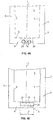
- Figure 4A shows a support base 2 whose edge portion 6 is provided with one pair of seats 23 with circular cross section, inside which respective cylindrical magnetic elements 17 are inserted.
- each seat a permanent magnet 24 obtained from a piece of permanent magnetic material having a cylindrical shape.
- a ferromagnetic metallic element 25 is applied to the second portion 15 of the flexible laminar element 7.
- This ferromagnetic metallic element is suited to interact with the magnetic element 17 integral with the edge portion 6 once the operator has coupled the unit assembly 14 with the support base 2.
- the ferromagnetic element 25 integral with the second portion 15 of the laminar element 7 can be a metallic plate (this time made of a metallic material which is not a permanent magnetic material).
- the protective film P can freely rotate around the hinge axis X between its terminal positions.
- the metallic plate 25 can be fixed to the second portion through an adhesive layer 19 previously spread on the latter.
- the dimensions l 1 , w 1 of said recess 20 are selected in such a way that they are substantially the same as the dimensions l 3 , w 3 of the ferromagnetic plate 25.
- the ferromagnetic plate 25 comes to be positioned inside the recess 20, so that the upper surface 8 of the flexible laminar element 7 is substantially flush with (or slightly above) the upper surface 22 of the edge portion 6.
- the ferromagnetic plate 25 can be inserted in the recess 20 with a relatively reduced play, in such a way as to define a fixed reference position of the unit assembly 14 with respect to the housing 3.
- the seats 23 obtained in the edge portion 6 of the base 2 can be substantially through seats and extend from the lower surface 26 of said base 2 to the bottom surface 27 of the recess 20.
- magnetic elements 17 can be used which are applied in a stable manner both to the second portion 15 of the laminar element 7 and to the edge portion 6 of the support base 2.
- the magnetic elements 18 anchored to the second portion 15 of the laminar element 7 can have opposite magnetic polarity with respect to the magnets 24 anchored to the edge portion 6 of the support base 2.
- the force F generated between the second portion 15 of the flexible laminar element 7 and the edge portion 6 will be an attraction force, so as to promote the movement of the unit assembly 14 towards the support base 2 and their removable mutual coupling.
- the operator provides for placing the electronic apparatus A inside the corresponding housing 3 formed in the support base 2.
- the operator promotes the adhesion of the first portion 12 of the lower surface 9 of the flexible laminar element 7 to the upper surface P" of the film P or, alternatively, to the layer of protective film that covers said surface (if provided).
- the first portion 12 of the lower surface 9 of the laminar element 7 can be applied to the film P in a previous step, so that the operator, when he/she intends to proceed with the application of the film P to the screen S of an electronic apparatus A, can already have at his/her disposal the unit assembly 14 which must simply be coupled with the support base 2 of the device 1.
- a magnetic element 17 and/or a metallic ferromagnetic element 25 designed to interact with the support base 2 are applied to the second portion 158 of the flexible laminar element.
- This magnetic force F is generated by the magnetic element 17 (or by the magnetic elements) which is integral with the edge portion 6 (for example, cylindrical permanent magnets 24) or integral with the second portion 23 of the laminar element 7 (for example, a magnetic plate 18).
- the magnetic element 17 and/or the ferromagnetic element 25 which is/are integral with the second portion 15 of the laminar element 7 can be inserted in the recess 20 formed in the support base 2, if said recess has been obtained in the latter.
- the operator will take care to remove said protective layer before promoting the contact between the film P and the screen S of the apparatus A.
- the operator can grasp the upper terminal projection 10 of the flexible laminar element 7 (on which no adhesive has been spread) in order to use it as an element on which it is possible to act to separate the laminar element 7 from the film P.
- the operator can remove the first portion 12 of the lower surface 9 of the laminar element 7 from the upper surface P' of the film P, actually eliminating from the latter the presence of any external element superimposed to it.
Landscapes
- Engineering & Computer Science (AREA)
- Manufacturing & Machinery (AREA)
- Electronic Switches (AREA)
- Telephone Set Structure (AREA)
- Casings For Electric Apparatus (AREA)
- Formation Of Insulating Films (AREA)
- Magnetic Heads (AREA)
- Apparatuses And Processes For Manufacturing Resistors (AREA)
Abstract
Description
- The present invention is related to the technical field of the accessories for electronic devices, and more specifically it concerns a device for applying a protective film to the screen of an electronic apparatus such as, for example, a smartphone, a tablet or a similar apparatus.
- As is known, the screens of mobile electronic devices such as, for example, smartphones, tablets, industrial readers and similar devices are made of glass-based composite materials and can be damaged or even break if their external surface is rubbed against hard objects or is subjected to hard impacts.
- Even if these screens substantially have the same chemical-physical characteristics as hardened glass, experience teaches that this component is still one of the most fragile components supplied together with electronic devices and the one which most of all needs to be replaced or repaired during the life cycle of said devices.
- In order to protect these devices from the drawbacks mentioned above it is possible to use transparent (or semi-transparent) protective films designed to be applied to the screen in a removable manner.
- These films have their lower surface covered with adhesive and intended to be superimposed to the external surface of the screen.
- The main drawback that occurs during the manual application of the film to the screen of the device is represented by the need to position the film correctly, aligning its edges with those of the screen.
- To obtain an optimal result, the user often needs to position the film on the screen several times and this may reduce the bonding power of the glue or increase the risk of fingerprints or marks being left on the surface of the screen or of the film.
- In order to overcome said drawback, some devices have been developed which are suited to make it easier to apply the film to the screen in an automatic or semiautomatic manner and are designed in such a way as to prevent any contact between the surfaces of the film and of the screen.
- Document
WO2015/021430 describes a method and a device for applying a protective film to the screen of an electronic apparatus, which comprises a polygonal base provided with a seat for housing the electronic apparatus. The protective film has its underside covered with glue and provided with a flexible tab made of a polymeric material and folded on itself which respectively has a lower brush and an end projecting from the upper edge of the film. The upper surface of the film is covered with a further protective layer on which a laminar projection has been applied, said laminar projection being provided with two holes suited to allow the insertion of two holes formed on the base in proximity to the seat. The engagement of the pins in said holes makes it possible to constrain the film to the body, while the traction force exerted by the user on the tab promotes the sliding movement of the brush on the screen and the adhesion of the glue to the screen. Once the projection has been extracted from the pins, the user can remove the upper layer positioned on the film. - A first drawback of this solution lies in that the insertion of the pins in the holes formed in the projection considerably slows down the operations required for the application of the protective film to the screen of the electronic apparatus.
- It is evident, in fact, that such a configuration of the applicator device requires a numerous sequence of actions to be carried out before the film can be actually applied to the screen.
- More specifically, the operator must insert the pins formed on the base in the holes made in the film or in the laminar tab and must also check that the latter does not come off the pins during the application of the film.
- Consequently, a further drawback associated with this solution is represented by the fact that the film is not firmly attached to the base during the application steps and this can affect the success of the operation.
- A further drawback of this solution is represented by the fact that it is rather complex and the application of a protective film to the screen of the electronic apparatus takes a relatively long time, which is often a nuisance for demanding users.
- Again, another and yet not the least inconvenience of this solution is represented by the fact that the complexity of the application of the protective film to the screen of the electronic apparatus increases the risk of the operator performing incorrect manoeuvres which may cause the film to adhere to the screen in a non-uniform manner and aesthetically unpleasant wrinkles and folds to appear.
- The present invention intends to overcome the drawbacks mentioned above by providing a device for applying a protective film to the screen of an electronic apparatus, wherein said device is particularly effective and flexible during use.
- More specifically, it is the main object of the present invention to provide a device for applying a protective film to the screen of an electronic apparatus which is easy to use and able to apply the film to the screen through a limited number of operations.
- It is a further object of the present invention to provide a device for applying a protective film to the screen of an electronic apparatus which is simple to produce.
- Again, it is another object of the present invention to provide a device for applying a protective film to a screen which guarantees a high degree of safety during use, preventing any of its parts from accidentally coming off during the application of the film to the screen.
- It is another, yet not the least object of the present invention to provide a device for applying a protective film to the screen of an electronic apparatus which is particularly economic and easy to produce.
- These objects, together with others that are explained in greater detail below, are achieved by a device for applying a protective film to the screen of an electronic apparatus of the type according to
claim 1. - Further objects that are better illustrated further on in this description are achieved by a device for applying a protective film to the screen of an electronic apparatus according to the dependent claims from 2 to 10.
- The advantages and the characteristics of the present invention clearly emerge from the following detailed description of some preferred but non-limiting configurations of a device for applying a protective film to the screen of an electronic apparatus, with particular reference to the following drawings:
-
Figure 1 shows an exploded perspective view of a device for applying a protective film to the screen of an electronic apparatus carried out according to a first embodiment; -
Figures 2A and2B respectively show a top view and a side view of a first detail of the device shown inFigure 1 ; -
Figures 3A and 3B show partial sectional side views of a further detail ofFigure 1 while it is being positioned on the support base; -
Figures 4A and 4B show top views of a support base of the device ofFigure 1 in two different operating configurations; -
Figure 4C shows a partial sectional side view of the support base shown inFigures 4A and 4B . - The subject of the present invention is a device for applying a protective film P to the screen S of an electronic apparatus A.
- Said device, indicated as a whole by the
reference number 1 in the drawings, can be particularly suited to allow a protective film P to be applied to the screen S of a smartphone, a tablet, a convertible notebook, an e-book reader and of all similar electronic apparatuses A. - Furthermore, said
device 1 can be configured to apply a protective film P to the screen S of the electronic apparatus A, wherein said protective film P can be of the flexible or rigid type, according to the preferences of the user of the device or of the owner of the apparatus. Furthermore, the film P can be completely transparent or of the semi-transparent type. - The protective film P has an upper surface P' and a lower surface P" to which an adhesive layer J is applied, said adhesive layer J being suited to allow the lower surface P" to adhere to the external surface S' of the screen S.
- The adhesive layer J can cover the lower surface P" of the film P completely or can be distributed only on a portion (or on several portions) of the same.
- The device comprises a
support base 2 provided with at least onehousing 3 for the positioning of the electronic apparatus A. - More specifically, the
support base 2 can have a substantially polygonal shape and on the same it will be possible to obtain ahousing 3 in a substantially rectangular shape, which is suited to allow the precise positioning of the electronic apparatus A, that is, to allow the latter to be positioned with a reduced play. - As is better clarified later on in this description, the relatively precise positioning of the electronic apparatus A in the
housing 3 makes it possible to define a fixed and stable position of the apparatus A with respect to the other components of thedevice 1 which are used during the operations required for the application of the film P. - In the configuration of the device illustrated in the figures, and more specifically in
Figure 1 and inFigures 4A and 4B , thesupport base 2 has ahousing 3 with fixed dimensions. - However, in different configurations of the device which are not visible in the figures the
housing 3 can have variable dimensions in order to allow electronic apparatuses of different sizes to be positioned therein, wherein the length and width of said apparatuses can vary between a minimum and a maximum predetermined value. - According to the invention, in order to obtain this result one or more
terminal edges edge 4 associated with the length of the electronic apparatus, or theedge 5 associated with its width, or bothedges 4, 5) can be movable with respect to thesupport base 2 between two predetermined terminal positions suited to define, respectively, the minimum and the maximum dimension of the apparatus A that allow the latter to be inserted in thehousing 3. - The
support base 2 furthermore comprises at least oneedge portion 6 extending on the periphery of thehousing 3. - More specifically, the
edge portion 6 formed on thebase 2 defines at least oneterminal edge housing 3. In the configuration of thesupport base 2 illustrated inFigure 1 there are fouredge portions 6 arranged peripherally on all sides of thehousing 3. - Thus, the latter is delimited by four
terminal edges housing 3. - Conveniently, the
device 1 comprises aflexible laminar element 7, better illustrated inFigures 2A and2B , provided with anupper surface 8 and alower surface 9. - The shape of the
laminar element 7 in a plan view can be substantially considered as a rectangle to which one pair ofterminal projections - The
lower surface 9 of thelaminar element 7 has afirst portion 12 at least partially covered with anadhesive layer 13 and intended to be superimposed to the upper surface P" of the film P in such a way as to form with the latter a unit assembly indicated by thereference number 14 inFigure 1 and inFigure 3A . - The
lower surface 9 of theflexible laminar element 7 has also asecond portion 16 arranged beside thefirst portion 12. - In the configuration of the laminar element illustrated in
Figure 2A , thefirst portion 12 of thelower surface 9 has a rather large extension, as it occupies almost the entirety of the area enclosed by the rectangular shape that defines the main part of thelaminar element 7. - The
upper projection 10 does not belong to thefirst portion 12 and therefore no adhesive is applied to the same. In this way, saidprojection 10 can be easily grasped by the user to remove theflexible laminar element 7 from the protective film P following the application of the latter to the screen S of the apparatus. - In
Figure 2A it is possible to observe also thesecond portion 15 of thelower surface 9, which substantially occupies the area enclosed by thelower projection 11 of theflexible laminar element 7. -
Means 16 are also provided, which are suited to promote the removable coupling of theunit assembly 14 with theedge portion 6 of the support base. - This coupling is suited to allow the protective film P to rotate around a predetermined hinge axis X.
- In the device illustrated in the figures the support base has a longitudinal development axis L and the hinge axis X lies substantially crosswise with respect to said development axis L.
- More specifically, during the use of the
device 1 the development axis L will be arranged in a substantially horizontal position and therefore the hinge axis X will be substantially parallel to the vertical. - The peculiar characteristic of the coupling means 16 lies in that they promote the selective and removable coupling of the
second portion 15 of the flexiblelaminar element 7 with theedge portion 6 formed on thebase 2. - This condition is clearly illustrated in
Figure 3A and inFigure 3B , in which it is possible to observe the coupling between theunit assembly 14 and theedge portion 6 formed on thesupport base 2. - More specifically,
Figure 3B illustrates the position of the protective film P before its application to the screen S of the electronic apparatus A. - The coupling means 16 are configured to allow the assembly 14 (and in particular the film P) to selectively rotate around the hinge axis X between an initial position, in which the film P is not in contact with the screen S, and a final position, in which the adhesive layer J distributed on the lower surface P" of the film P is in contact with the upper surface S' of the screen S.
-
Figure 3A shows the film P in the initial position, whileFigure 3B shows the film P in the final position. - In other words, the coupling means 16 are able to promote the rotation of the
assembly 14 around the hinge axis X over an angular amplitude Δθ smaller than a straight angle (and typically close to a right angle); it is evident that this angular amplitude Δθ is delimited by the initial and final position of the film P. - According to a peculiar aspect of the invention, the coupling means 16 comprise at least one
magnetic element 17 associated with thesecond portion 15 of the flexiblelaminar element 7 and/or with thecorresponding edge portion 6 formed on thesupport base 2. - In the configuration of the device illustrated in the Figures from 2A to 3B, there is a single
magnetic element 17 associated with thesecond portion 15 of thelaminar element 7. - In this case the
magnetic element 17 is constituted by a substantially laminarmetallic plate 18 that completely covers thesecond portion 15 of thelower surface 9 of the flexiblelaminar element 7. - This
plate 18 can be a permanent magnet or an element obtained from a permanent magnetic material such as, for example, neodymium or other rare-earth elements similar to it. - More specifically, as is better visible in
Figures 2B and 3A , thesecond portion 15 is covered by a thinadhesive layer 19 suited to promote the stable coupling of themagnetic element 18, that is, of themetallic plate 19, with thelower surface 9 of the flexiblelaminar element 7. - The
magnetic plate 18 is configured to interact with thecorresponding edge portion 6 in such a way as to removably hold theunit assembly 14 on thebase 2. - More specifically, the area of the
edge portion 6 designed to be coupled with themagnetic plate 18 is made of a ferromagnetic material. - When these two components are at a close distance from each other, an attraction force F is generated which acts on the
plate 18 and is directed towards thebase 2; said force F, illustrated inFigure 3A , causes thecomponents - The magnetic force F that maintains the
plate 18 in contact with thebase 2 thus makes it possible to maintain thebase 2 substantially coupled with theunit assembly 14 in a removable manner. - Conveniently, it is rather common to make the
entire edge portion 6 or theentire support base 2 from a ferromagnetic material (ferrous alloys, steel, etc). - When the
magnetic plate 18 is coupled with thebase 2, the protective film P is free to selectively rotate around the hinge axis X between its initial position and its final position, as better illustrated inFigures 3A and 3B . - In order to increase the magnetic force F generated by the coupling means 16, it is possible to use several magnetic elements 17 (for example, magnetic plates 18) superimposed to one another and positioned in proximity of the
second portion 15 of thelower surface 9 of the flexiblelaminar element 7. - The
edge portion 6 can be provided with a shaped recess, indicated by thereference number 20 in the figures, which is positioned in proximity to the area where it interacts with thesecond portion 15 of thelower surface 9 of the flexiblelaminar element 7. - More specifically, the dimensions l1, w1 of said
recess 20 are selected in such a way that they are substantially the same as the dimensions l2, w2 of themagnetic element 17, that is, as the dimensions of theplate 18. - In this way, when the operator promotes the coupling of the
unit assembly 14 with theedge portion 6, themagnetic plate 18 comes to be positioned inside therecess 20, so that theupper surface 8 of the flexiblelaminar element 7 is substantially flush with (or slightly above) theupper surface 22 of theedge portion 6. - This condition is clearly visible in
Figure 3B . - Preferably, the
magnetic plate 18 can be inserted in therecess 20 with a relatively reduced play, in such a way as to define a fixed reference position of theunit assembly 14 with respect to thehousing 3. - In an alternative configuration of the
device 1, illustrated in Figures from 4A to 4C, severalmagnetic elements 17 are used, in this case associated with theedge portion 6 of thesupport base 2. - More specifically, said
magnetic elements 17 are positioned in theedge portion 6 in proximity to the area where the latter interacts with thesecond portion 15 of the flexiblelaminar element 7. - On the
edge portion 6 there can be one ormore seats 23 which are suitable for the insertion of correspondingmagnetic elements 17. -
Figure 4A shows asupport base 2 whoseedge portion 6 is provided with one pair ofseats 23 with circular cross section, inside which respective cylindricalmagnetic elements 17 are inserted. - For example, it will be possible to insert inside each seat a
permanent magnet 24 obtained from a piece of permanent magnetic material having a cylindrical shape. - This condition can be observed in
Figure 4C , however it should be underlined that the shape of theseat 23, the shape of themagnetic elements 24 and the number of the latter can be different from those illustrated in the Figures and can vary according to the construction and/or operational needs associated with thespecific device 1. - More specifically, the larger the number of
magnetic elements 17 inserted in theseats 23, the stronger the magnetic attraction force F generated by the same on thesecond portion 15 of thelower surface 9 of the flexiblelaminar element 7. - The result is thus evident, since an increase in the number of
magnetic elements 17 included in thedevice 1 will result in a corresponding increase of the coupling force F generated between theunit assembly 14 and theedge portion 6 of thesupport base 2. - According to the configuration of the device illustrated in Figures from 4A to 4C, a ferromagnetic
metallic element 25 is applied to thesecond portion 15 of the flexiblelaminar element 7. - This ferromagnetic metallic element is suited to interact with the
magnetic element 17 integral with theedge portion 6 once the operator has coupled theunit assembly 14 with thesupport base 2. - More specifically, also in this case the
ferromagnetic element 25 integral with thesecond portion 15 of thelaminar element 7 can be a metallic plate (this time made of a metallic material which is not a permanent magnetic material). - Similarly to what has already been described with reference to the first configuration of the invention, when the distance d that separates the
metallic plate 25 from theedge portion 6 is relatively reduced, a magnetic force F acting on theferromagnetic plate 25 and directed towards theedge portion 6 is generated between said two components. - When the
plate 25 is in contact with theedge portion 6, the value of this magnetic attraction force F is sufficient to promote the stable and removable coupling of theunit assembly 14 with theedge portion 6, that is, with thesupport base 2. - In these conditions, the protective film P can freely rotate around the hinge axis X between its terminal positions.
- The
metallic plate 25 can be fixed to the second portion through anadhesive layer 19 previously spread on the latter. - According to the invention, also in this configuration there can be a
recess 20 formed on theedge portion 6 and suited to allow the insertion of themetallic plate 25 once theunit assembly 14 has been coupled with thesupport base 2. - More specifically, the dimensions l1, w1 of said
recess 20 are selected in such a way that they are substantially the same as the dimensions l3, w3 of theferromagnetic plate 25. - In this way, when the operator carries out the coupling between the
unit assembly 14 and theedge portion 6, theferromagnetic plate 25 comes to be positioned inside therecess 20, so that theupper surface 8 of the flexiblelaminar element 7 is substantially flush with (or slightly above) theupper surface 22 of theedge portion 6. - Preferably, the
ferromagnetic plate 25 can be inserted in therecess 20 with a relatively reduced play, in such a way as to define a fixed reference position of theunit assembly 14 with respect to thehousing 3. - As is better visible in
Figure 4C , theseats 23 obtained in theedge portion 6 of thebase 2 can be substantially through seats and extend from thelower surface 26 of saidbase 2 to thebottom surface 27 of therecess 20. - According to the invention, in a further configuration of the device (not illustrated in the figures)
magnetic elements 17 can be used which are applied in a stable manner both to thesecond portion 15 of thelaminar element 7 and to theedge portion 6 of thesupport base 2. - In this case, therefore, the
magnetic elements 18 anchored to thesecond portion 15 of thelaminar element 7 can have opposite magnetic polarity with respect to themagnets 24 anchored to theedge portion 6 of thesupport base 2. - In this way, the force F generated between the
second portion 15 of the flexiblelaminar element 7 and theedge portion 6 will be an attraction force, so as to promote the movement of theunit assembly 14 towards thesupport base 2 and their removable mutual coupling. - From the operational point of view, firstly the operator provides for placing the electronic apparatus A inside the
corresponding housing 3 formed in thesupport base 2. - Successively, the operator promotes the adhesion of the
first portion 12 of thelower surface 9 of the flexiblelaminar element 7 to the upper surface P" of the film P or, alternatively, to the layer of protective film that covers said surface (if provided). - This adhesion promotes the formation of a
unit assembly 14 which in a successive step will be coupled with theedge portion 6 formed on thebase 6. - While positioning the
first portion 12 of thelaminar element 7 so that it adheres to the upper surface P" of the film P, the operator must take care to maintain thesecond portion 15 of thelower surface 9 of thelaminar element 7 in a projecting position with respect to the external edge B of the film P. - Alternatively, the
first portion 12 of thelower surface 9 of thelaminar element 7 can be applied to the film P in a previous step, so that the operator, when he/she intends to proceed with the application of the film P to the screen S of an electronic apparatus A, can already have at his/her disposal theunit assembly 14 which must simply be coupled with thesupport base 2 of thedevice 1. - In fact, a
magnetic element 17 and/or a metallicferromagnetic element 25 designed to interact with thesupport base 2 are applied to the second portion 158 of the flexible laminar element. - At this point the operator manually moves the
second portion 15 towards theedge portion 2, wherein these two elements must be moved towards each other until a mutual magnetic attraction force F is generated between them. - This magnetic force F is generated by the magnetic element 17 (or by the magnetic elements) which is integral with the edge portion 6 (for example, cylindrical permanent magnets 24) or integral with the
second portion 23 of the laminar element 7 (for example, a magnetic plate 18). - The action of said force F promotes the automatic and spontaneous contact of the
second portion 15 of thelower surface 9 of thelaminar element 7 with theedge portion 6. - The
magnetic element 17 and/or theferromagnetic element 25 which is/are integral with thesecond portion 15 of thelaminar element 7 can be inserted in therecess 20 formed in thesupport base 2, if said recess has been obtained in the latter. - Following said contact, a stable (but removable) coupling between the
unit assembly 14 and thebase 2 is generated, and therefore in these conditions the operator can promote the rotation of the film P around the hinge axis X from the detached terminal position to the position of contact with the upper surface S' of the screen S. - If the film P is provided with a lower protective layer suited to protect the adhesive, the operator will take care to remove said protective layer before promoting the contact between the film P and the screen S of the apparatus A.
- A slight pressure exerted by the operator with his/her fingers on the upper surface of the film P' will make it possible to obtain the uniform adhesion of the adhesive layer J spread on its lower surface P" to the screen S of the apparatus A.
- At the end of this operation, the operator can grasp the
upper terminal projection 10 of the flexible laminar element 7 (on which no adhesive has been spread) in order to use it as an element on which it is possible to act to separate thelaminar element 7 from the film P. - By applying a traction force towards the outside on said
projection 10, the operator can remove thefirst portion 12 of thelower surface 9 of thelaminar element 7 from the upper surface P' of the film P, actually eliminating from the latter the presence of any external element superimposed to it. - At this point the operator can extract the apparatus A from the
housing 3 formed in thesupport base 2, since the film is now applied to the screen S of the apparatus A in a stable manner and it is no more necessary to use thedevice 1. - The present invention can be carried out in other variants, all falling within the scope of the inventive characteristics claimed and described herein; these technical features can be replaced by different technically equivalent elements and materials; the shape and size of the invention can be any, provided that they are compatible with its intended use.
- The reference numbers and signs included in the claims and in the description have the only purpose to increase the intelligibility of the text and must not be considered as elements limiting the technical interpretation of the objects or processes they identify.
Claims (10)
- A device for applying a protective film (P) to the screen (S) of an electronic apparatus (A), wherein the protective film (P) has an upper surface (P') and a lower surface (P") at least partially covered by an adhesive layer (J) intended to be applied to the screen (S) of the apparatus (A), said device comprising:- a support base (2) provided with at least one housing (3) for the positioning of the electronic apparatus (A);- at least one edge portion (6) formed in said support base (2) and arranged on the periphery of said at least one housing (3);- a flexible laminar element (7) with a lower surface (9) provided with a first portion (12) at least partially covered with an adhesive layer (13) and with a second portion (15) placed beside said first portion (12), said first portion (12) being intended to be superimposed to the upper surface (P') of the film (P) in such a way as to create a unit assembly (14) with the latter;- means (16) for the selective coupling of said unit assembly (14) with said at least one edge portion (6), said coupling means (16) being suited to allow the protective film (P) to selectively rotate around a predetermined hinge axis (X);wherein said coupling means (16) are designed to promote the selective and removable coupling of the second portion (15) of the lower surface (9) of said flexible laminar element (7) with said at least one edge portion (6) of said support base (2);
characterized in that said coupling means (16) comprise at least one magnetic element (17) associated with said second portion (15) of the lower surface (9) of said flexible laminar element (7) and/or with said at least one edge portion (6) of said base (P). - Device according to claim 1, characterized in that at least the area of said at least one edge portion (6) designed to be coupled with said second portion (15) of said flexible laminar element (7) is made of a metallic ferromagnetic material.
- Device according to claim 2, characterized in that said at least one magnetic element (17) is integral with the second portion (15) of said flexible laminar element (7) and is suited to interact with the coupling area of said at least one ferromagnetic edge portion (6) made of a ferromagnetic material to promote the removable restraint of said unit assembly (14) to said support base (2).
- Device according to claim 3, characterized in that said second portion (15) of said flexible laminar element (7) is covered by an adhesive layer (6) in such a way as to allow it to be anchored to said at least one magnetic element (17).
- Device according to one or more of the previous claims, characterized in that said at least one magnetic element (17) is made up of one or more permanent magnets, each of said permanent magnets being constituted by a substantially laminar plate (18).
- Device according to claim 1, characterized in that said coupling means (16) comprise at least one magnetic element (17) integral with said at least one edge portion (6) of said base (2), said at least one magnetic element (17) being placed substantially in proximity to the coupling area between said second portion (15) of said laminar element (7) and said at least one edge portion (6).
- Device according to claim 6, characterized in that said at least one edge portion (6) comprises one or more seats (23) designed to house said at least one magnetic element (17).
- Device according to claim 6 or 7, characterized in that said coupling means (16) comprise a metallic ferromagnetic element (25) integral with said second portion (15) of said flexible laminar element (7), said metallic ferromagnetic element (25) being intended to interact with said at least one magnetic element (17) housed in said one or more seats (23).
- Device according to one or more of the previous claims, characterized in that said at least one edge portion (6) has a shaped recess (20) positioned in proximity to the area where it is coupled with said second portion (15) of said flexible laminar element (7).
- Device according to claim 9, characterized in that the dimensions (l1, w1) of said recess (20) are substantially equal to the dimensions (l2, w2 ; l3, w3) of said magnetic element (17) or of said metallic ferromagnetic element (25) which are integral with said second portion (15) in such a way as to allow said element (17, 25) to be inserted in said recess (20) in order to position the upper surface (8) of said flexible laminar element (7) substantially flush with the upper surface (22) of said at least one edge portion (6) once said unit assembly (14) has been coupled with said support base (2).
Priority Applications (3)
| Application Number | Priority Date | Filing Date | Title |
|---|---|---|---|
| RS20220721A RS63466B1 (en) | 2019-07-17 | 2020-07-16 | DEVICE FOR APPLYING A PROTECTIVE FOIL ON THE SCREEN OF AN ELECTRONIC DEVICE |
| HRP20220938TT HRP20220938T1 (en) | 2019-07-17 | 2020-07-16 | Device for applying a protective film on a screen of an electronic apparatus |
| SI202030077T SI3766665T1 (en) | 2019-07-17 | 2020-07-16 | Device for applying a protective film on a screen of an electronic apparatus |
Applications Claiming Priority (1)
| Application Number | Priority Date | Filing Date | Title |
|---|---|---|---|
| IT102019000012204A IT201900012204A1 (en) | 2019-07-17 | 2019-07-17 | DEVICE FOR THE APPLICATION OF A PROTECTIVE FILM ON THE SCREEN OF AN ELECTRONIC DEVICE |
Publications (2)
| Publication Number | Publication Date |
|---|---|
| EP3766665A1 true EP3766665A1 (en) | 2021-01-20 |
| EP3766665B1 EP3766665B1 (en) | 2022-05-18 |
Family
ID=68582209
Family Applications (1)
| Application Number | Title | Priority Date | Filing Date |
|---|---|---|---|
| EP20186288.5A Active EP3766665B1 (en) | 2019-07-17 | 2020-07-16 | Device for applying a protective film on a screen of an electronic apparatus |
Country Status (10)
| Country | Link |
|---|---|
| EP (1) | EP3766665B1 (en) |
| ES (1) | ES2925452T3 (en) |
| HR (1) | HRP20220938T1 (en) |
| HU (1) | HUE059295T2 (en) |
| IT (1) | IT201900012204A1 (en) |
| LT (1) | LT3766665T (en) |
| PL (1) | PL3766665T3 (en) |
| PT (1) | PT3766665T (en) |
| RS (1) | RS63466B1 (en) |
| SI (1) | SI3766665T1 (en) |
Cited By (2)
| Publication number | Priority date | Publication date | Assignee | Title |
|---|---|---|---|---|
| CN114953415A (en) * | 2022-04-18 | 2022-08-30 | 江苏吉福新材料股份有限公司 | Building decorative panel tectorial membrane device |
| CN115223445A (en) * | 2021-04-21 | 2022-10-21 | 鸿富锦精密工业(武汉)有限公司 | Display and packing box thereof |
Citations (2)
| Publication number | Priority date | Publication date | Assignee | Title |
|---|---|---|---|---|
| WO2015021430A1 (en) | 2013-08-08 | 2015-02-12 | Belkin International, Inc | Overlay applicator, applicator machine, and cradle, and method of providing and using the same |
| EP3381655A1 (en) * | 2017-03-31 | 2018-10-03 | Chia-Ching Lin | Screen film applicator |
-
2019
- 2019-07-17 IT IT102019000012204A patent/IT201900012204A1/en unknown
-
2020
- 2020-07-16 LT LTEP20186288.5T patent/LT3766665T/en unknown
- 2020-07-16 SI SI202030077T patent/SI3766665T1/en unknown
- 2020-07-16 PT PT201862885T patent/PT3766665T/en unknown
- 2020-07-16 HR HRP20220938TT patent/HRP20220938T1/en unknown
- 2020-07-16 HU HUE20186288A patent/HUE059295T2/en unknown
- 2020-07-16 RS RS20220721A patent/RS63466B1/en unknown
- 2020-07-16 ES ES20186288T patent/ES2925452T3/en active Active
- 2020-07-16 EP EP20186288.5A patent/EP3766665B1/en active Active
- 2020-07-16 PL PL20186288.5T patent/PL3766665T3/en unknown
Patent Citations (2)
| Publication number | Priority date | Publication date | Assignee | Title |
|---|---|---|---|---|
| WO2015021430A1 (en) | 2013-08-08 | 2015-02-12 | Belkin International, Inc | Overlay applicator, applicator machine, and cradle, and method of providing and using the same |
| EP3381655A1 (en) * | 2017-03-31 | 2018-10-03 | Chia-Ching Lin | Screen film applicator |
Cited By (4)
| Publication number | Priority date | Publication date | Assignee | Title |
|---|---|---|---|---|
| CN115223445A (en) * | 2021-04-21 | 2022-10-21 | 鸿富锦精密工业(武汉)有限公司 | Display and packing box thereof |
| CN115223445B (en) * | 2021-04-21 | 2023-12-12 | 鸿富锦精密工业(武汉)有限公司 | Monitor and its packaging box |
| CN114953415A (en) * | 2022-04-18 | 2022-08-30 | 江苏吉福新材料股份有限公司 | Building decorative panel tectorial membrane device |
| CN114953415B (en) * | 2022-04-18 | 2023-02-10 | 江苏吉福新材料股份有限公司 | Building decorative panel tectorial membrane device |
Also Published As
| Publication number | Publication date |
|---|---|
| RS63466B1 (en) | 2022-08-31 |
| EP3766665B1 (en) | 2022-05-18 |
| PT3766665T (en) | 2022-08-02 |
| LT3766665T (en) | 2022-08-25 |
| HRP20220938T1 (en) | 2022-10-28 |
| PL3766665T3 (en) | 2022-09-26 |
| HUE059295T2 (en) | 2022-11-28 |
| IT201900012204A1 (en) | 2021-01-17 |
| SI3766665T1 (en) | 2022-10-28 |
| ES2925452T3 (en) | 2022-10-18 |
Similar Documents
| Publication | Publication Date | Title |
|---|---|---|
| EP3766665B1 (en) | Device for applying a protective film on a screen of an electronic apparatus | |
| KR200483552Y1 (en) | Display protection film attatching case for mobile terminal | |
| EP2891552A1 (en) | An applicator | |
| US9731531B2 (en) | Craftwork tools and kits | |
| US9776443B1 (en) | Craftwork tools and kits | |
| CN108135339B (en) | Tablet computer housing and manufacturing method | |
| US11338525B2 (en) | Systems and methods for mobile device surface protection | |
| EP2940880A2 (en) | Accessory and control method | |
| KR20160022665A (en) | Sliding type display protection film attatching case for mobile terminal | |
| US10743637B2 (en) | Housing for cosmetic product | |
| WO2016204172A1 (en) | Protection film adhering jig | |
| EP3677427A1 (en) | Overlay applicator | |
| WO2019135082A1 (en) | A combination of an applicator and a screen protector | |
| US10328356B1 (en) | Assembling beads on a beading board | |
| KR101462266B1 (en) | Screen protective film attaching method using by application | |
| KR20140004440A (en) | Lcd protection film affixed to the device and how to attach the lcd protection film using this | |
| CA1132164A (en) | Device for dry transfer at ink patterns | |
| KR101804399B1 (en) | Punching device capable of changing hole shape | |
| KR20170004090A (en) | Wallet | |
| JP2021511978A (en) | Stamping tool | |
| KR101783169B1 (en) | folding package capable of storage card | |
| GB2531901A (en) | An electronic device holder | |
| JP6120034B1 (en) | Mobile phone case | |
| KR20200094111A (en) | Mobile Device Case Integral Fingerstrap | |
| JP6580896B2 (en) | Portable electronic device protective equipment |
Legal Events
| Date | Code | Title | Description |
|---|---|---|---|
| REG | Reference to a national code |
Ref country code: HR Ref legal event code: TUEP Ref document number: P20220938 Country of ref document: HR |
|
| PUAI | Public reference made under article 153(3) epc to a published international application that has entered the european phase |
Free format text: ORIGINAL CODE: 0009012 |
|
| STAA | Information on the status of an ep patent application or granted ep patent |
Free format text: STATUS: THE APPLICATION HAS BEEN PUBLISHED |
|
| AK | Designated contracting states |
Kind code of ref document: A1 Designated state(s): AL AT BE BG CH CY CZ DE DK EE ES FI FR GB GR HR HU IE IS IT LI LT LU LV MC MK MT NL NO PL PT RO RS SE SI SK SM TR |
|
| AX | Request for extension of the european patent |
Extension state: BA ME |
|
| STAA | Information on the status of an ep patent application or granted ep patent |
Free format text: STATUS: REQUEST FOR EXAMINATION WAS MADE |
|
| 17P | Request for examination filed |
Effective date: 20210319 |
|
| RBV | Designated contracting states (corrected) |
Designated state(s): AL AT BE BG CH CY CZ DE DK EE ES FI FR GB GR HR HU IE IS IT LI LT LU LV MC MK MT NL NO PL PT RO RS SE SI SK SM TR |
|
| GRAP | Despatch of communication of intention to grant a patent |
Free format text: ORIGINAL CODE: EPIDOSNIGR1 |
|
| STAA | Information on the status of an ep patent application or granted ep patent |
Free format text: STATUS: GRANT OF PATENT IS INTENDED |
|
| INTG | Intention to grant announced |
Effective date: 20211215 |
|
| GRAS | Grant fee paid |
Free format text: ORIGINAL CODE: EPIDOSNIGR3 |
|
| GRAA | (expected) grant |
Free format text: ORIGINAL CODE: 0009210 |
|
| STAA | Information on the status of an ep patent application or granted ep patent |
Free format text: STATUS: THE PATENT HAS BEEN GRANTED |
|
| AK | Designated contracting states |
Kind code of ref document: B1 Designated state(s): AL AT BE BG CH CY CZ DE DK EE ES FI FR GB GR HR HU IE IS IT LI LT LU LV MC MK MT NL NO PL PT RO RS SE SI SK SM TR |
|
| REG | Reference to a national code |
Ref country code: GB Ref legal event code: FG4D |
|
| REG | Reference to a national code |
Ref country code: CH Ref legal event code: EP |
|
| REG | Reference to a national code |
Ref country code: IE Ref legal event code: FG4D |
|
| REG | Reference to a national code |
Ref country code: DE Ref legal event code: R096 Ref document number: 602020003220 Country of ref document: DE |
|
| REG | Reference to a national code |
Ref country code: AT Ref legal event code: REF Ref document number: 1492909 Country of ref document: AT Kind code of ref document: T Effective date: 20220615 |
|
| REG | Reference to a national code |
Ref country code: PT Ref legal event code: SC4A Ref document number: 3766665 Country of ref document: PT Date of ref document: 20220802 Kind code of ref document: T Free format text: AVAILABILITY OF NATIONAL TRANSLATION Effective date: 20220728 |
|
| REG | Reference to a national code |
Ref country code: RO Ref legal event code: EPE |
|
| REG | Reference to a national code |
Ref country code: NL Ref legal event code: FP |
|
| REG | Reference to a national code |
Ref country code: SE Ref legal event code: TRGR |
|
| REG | Reference to a national code |
Ref country code: NO Ref legal event code: T2 Effective date: 20220518 |
|
| REG | Reference to a national code |
Ref country code: HR Ref legal event code: ODRP Ref document number: P20220938 Country of ref document: HR Payment date: 20220808 Year of fee payment: 3 |
|
| REG | Reference to a national code |
Ref country code: ES Ref legal event code: FG2A Ref document number: 2925452 Country of ref document: ES Kind code of ref document: T3 Effective date: 20221018 |
|
| REG | Reference to a national code |
Ref country code: HR Ref legal event code: T1PR Ref document number: P20220938 Country of ref document: HR |
|
| PG25 | Lapsed in a contracting state [announced via postgrant information from national office to epo] |
Ref country code: GR Free format text: LAPSE BECAUSE OF FAILURE TO SUBMIT A TRANSLATION OF THE DESCRIPTION OR TO PAY THE FEE WITHIN THE PRESCRIBED TIME-LIMIT Effective date: 20220819 Ref country code: FI Free format text: LAPSE BECAUSE OF FAILURE TO SUBMIT A TRANSLATION OF THE DESCRIPTION OR TO PAY THE FEE WITHIN THE PRESCRIBED TIME-LIMIT Effective date: 20220518 Ref country code: BG Free format text: LAPSE BECAUSE OF FAILURE TO SUBMIT A TRANSLATION OF THE DESCRIPTION OR TO PAY THE FEE WITHIN THE PRESCRIBED TIME-LIMIT Effective date: 20220818 |
|
| REG | Reference to a national code |
Ref country code: HU Ref legal event code: AG4A Ref document number: E059295 Country of ref document: HU |
|
| PG25 | Lapsed in a contracting state [announced via postgrant information from national office to epo] |
Ref country code: IS Free format text: LAPSE BECAUSE OF FAILURE TO SUBMIT A TRANSLATION OF THE DESCRIPTION OR TO PAY THE FEE WITHIN THE PRESCRIBED TIME-LIMIT Effective date: 20220918 |
|
| PG25 | Lapsed in a contracting state [announced via postgrant information from national office to epo] |
Ref country code: SM Free format text: LAPSE BECAUSE OF FAILURE TO SUBMIT A TRANSLATION OF THE DESCRIPTION OR TO PAY THE FEE WITHIN THE PRESCRIBED TIME-LIMIT Effective date: 20220518 Ref country code: SK Free format text: LAPSE BECAUSE OF FAILURE TO SUBMIT A TRANSLATION OF THE DESCRIPTION OR TO PAY THE FEE WITHIN THE PRESCRIBED TIME-LIMIT Effective date: 20220518 Ref country code: EE Free format text: LAPSE BECAUSE OF FAILURE TO SUBMIT A TRANSLATION OF THE DESCRIPTION OR TO PAY THE FEE WITHIN THE PRESCRIBED TIME-LIMIT Effective date: 20220518 Ref country code: DK Free format text: LAPSE BECAUSE OF FAILURE TO SUBMIT A TRANSLATION OF THE DESCRIPTION OR TO PAY THE FEE WITHIN THE PRESCRIBED TIME-LIMIT Effective date: 20220518 |
|
| REG | Reference to a national code |
Ref country code: DE Ref legal event code: R097 Ref document number: 602020003220 Country of ref document: DE |
|
| PG25 | Lapsed in a contracting state [announced via postgrant information from national office to epo] |
Ref country code: MC Free format text: LAPSE BECAUSE OF FAILURE TO SUBMIT A TRANSLATION OF THE DESCRIPTION OR TO PAY THE FEE WITHIN THE PRESCRIBED TIME-LIMIT Effective date: 20220518 |
|
| PLBE | No opposition filed within time limit |
Free format text: ORIGINAL CODE: 0009261 |
|
| STAA | Information on the status of an ep patent application or granted ep patent |
Free format text: STATUS: NO OPPOSITION FILED WITHIN TIME LIMIT |
|
| PG25 | Lapsed in a contracting state [announced via postgrant information from national office to epo] |
Ref country code: AL Free format text: LAPSE BECAUSE OF FAILURE TO SUBMIT A TRANSLATION OF THE DESCRIPTION OR TO PAY THE FEE WITHIN THE PRESCRIBED TIME-LIMIT Effective date: 20220518 |
|
| 26N | No opposition filed |
Effective date: 20230221 |
|
| PG25 | Lapsed in a contracting state [announced via postgrant information from national office to epo] |
Ref country code: LU Free format text: LAPSE BECAUSE OF NON-PAYMENT OF DUE FEES Effective date: 20220716 |
|
| P01 | Opt-out of the competence of the unified patent court (upc) registered |
Effective date: 20230531 |
|
| REG | Reference to a national code |
Ref country code: HR Ref legal event code: ODRP Ref document number: P20220938 Country of ref document: HR Payment date: 20230714 Year of fee payment: 4 |
|
| REG | Reference to a national code |
Ref country code: AT Ref legal event code: UEP Ref document number: 1492909 Country of ref document: AT Kind code of ref document: T Effective date: 20220518 |
|
| PG25 | Lapsed in a contracting state [announced via postgrant information from national office to epo] |
Ref country code: CY Free format text: LAPSE BECAUSE OF FAILURE TO SUBMIT A TRANSLATION OF THE DESCRIPTION OR TO PAY THE FEE WITHIN THE PRESCRIBED TIME-LIMIT Effective date: 20220511 |
|
| PGFP | Annual fee paid to national office [announced via postgrant information from national office to epo] |
Ref country code: GB Payment date: 20240619 Year of fee payment: 5 |
|
| PGFP | Annual fee paid to national office [announced via postgrant information from national office to epo] |
Ref country code: FR Payment date: 20240618 Year of fee payment: 5 |
|
| REG | Reference to a national code |
Ref country code: HR Ref legal event code: ODRP Ref document number: P20220938 Country of ref document: HR Payment date: 20240710 Year of fee payment: 5 |
|
| PGFP | Annual fee paid to national office [announced via postgrant information from national office to epo] |
Ref country code: NL Payment date: 20240726 Year of fee payment: 5 |
|
| PGFP | Annual fee paid to national office [announced via postgrant information from national office to epo] |
Ref country code: IT Payment date: 20240617 Year of fee payment: 5 |
|
| PGFP | Annual fee paid to national office [announced via postgrant information from national office to epo] |
Ref country code: HR Payment date: 20240710 Year of fee payment: 5 Ref country code: DE Payment date: 20240618 Year of fee payment: 5 Ref country code: LT Payment date: 20240708 Year of fee payment: 5 Ref country code: IE Payment date: 20240704 Year of fee payment: 5 |
|
| PGFP | Annual fee paid to national office [announced via postgrant information from national office to epo] |
Ref country code: PT Payment date: 20240705 Year of fee payment: 5 |
|
| PGFP | Annual fee paid to national office [announced via postgrant information from national office to epo] |
Ref country code: BE Payment date: 20240726 Year of fee payment: 5 |
|
| PGFP | Annual fee paid to national office [announced via postgrant information from national office to epo] |
Ref country code: ES Payment date: 20240801 Year of fee payment: 5 Ref country code: CH Payment date: 20240801 Year of fee payment: 5 |
|
| PGFP | Annual fee paid to national office [announced via postgrant information from national office to epo] |
Ref country code: CZ Payment date: 20240711 Year of fee payment: 5 |
|
| PGFP | Annual fee paid to national office [announced via postgrant information from national office to epo] |
Ref country code: PL Payment date: 20240711 Year of fee payment: 5 |
|
| PGFP | Annual fee paid to national office [announced via postgrant information from national office to epo] |
Ref country code: HU Payment date: 20240725 Year of fee payment: 5 Ref country code: SI Payment date: 20240710 Year of fee payment: 5 |
|
| PGFP | Annual fee paid to national office [announced via postgrant information from national office to epo] |
Ref country code: LV Payment date: 20240723 Year of fee payment: 5 |
|
| PGFP | Annual fee paid to national office [announced via postgrant information from national office to epo] |
Ref country code: RO Payment date: 20240712 Year of fee payment: 5 Ref country code: NO Payment date: 20240704 Year of fee payment: 5 Ref country code: RS Payment date: 20240709 Year of fee payment: 5 Ref country code: SE Payment date: 20240711 Year of fee payment: 5 |
|
| PG25 | Lapsed in a contracting state [announced via postgrant information from national office to epo] |
Ref country code: BG Free format text: LAPSE BECAUSE OF FAILURE TO SUBMIT A TRANSLATION OF THE DESCRIPTION OR TO PAY THE FEE WITHIN THE PRESCRIBED TIME-LIMIT Effective date: 20220518 |
|
| PG25 | Lapsed in a contracting state [announced via postgrant information from national office to epo] |
Ref country code: BG Free format text: LAPSE BECAUSE OF FAILURE TO SUBMIT A TRANSLATION OF THE DESCRIPTION OR TO PAY THE FEE WITHIN THE PRESCRIBED TIME-LIMIT Effective date: 20220518 |
|
| PGFP | Annual fee paid to national office [announced via postgrant information from national office to epo] |
Ref country code: MT Payment date: 20240729 Year of fee payment: 5 |
|
| PGFP | Annual fee paid to national office [announced via postgrant information from national office to epo] |
Ref country code: AT Payment date: 20251020 Year of fee payment: 5 |
|
| PGFP | Annual fee paid to national office [announced via postgrant information from national office to epo] |
Ref country code: MK Payment date: 20240712 Year of fee payment: 5 |
|
| PG25 | Lapsed in a contracting state [announced via postgrant information from national office to epo] |
Ref country code: TR Free format text: LAPSE BECAUSE OF FAILURE TO SUBMIT A TRANSLATION OF THE DESCRIPTION OR TO PAY THE FEE WITHIN THE PRESCRIBED TIME-LIMIT Effective date: 20220518 |
|
| REG | Reference to a national code |
Ref country code: HR Ref legal event code: PBON Ref document number: P20220938 Country of ref document: HR Effective date: 20250716 |
|
| REG | Reference to a national code |
Ref country code: DE Ref legal event code: R119 Ref document number: 602020003220 Country of ref document: DE |
|
| REG | Reference to a national code |
Ref country code: LT Ref legal event code: MM4D Effective date: 20250716 |
|
| REG | Reference to a national code |
Ref country code: CH Ref legal event code: H13 Free format text: ST27 STATUS EVENT CODE: U-0-0-H10-H13 (AS PROVIDED BY THE NATIONAL OFFICE) Effective date: 20260224 |
|
| REG | Reference to a national code |
Ref country code: NL Ref legal event code: MM Effective date: 20250801 |
|
| PG25 | Lapsed in a contracting state [announced via postgrant information from national office to epo] |
Ref country code: HU Free format text: LAPSE BECAUSE OF NON-PAYMENT OF DUE FEES Effective date: 20250717 |
|
| GBPC | Gb: european patent ceased through non-payment of renewal fee |
Effective date: 20250716 |
|
| REG | Reference to a national code |
Ref country code: BE Ref legal event code: MM Effective date: 20250731 |
|
| PG25 | Lapsed in a contracting state [announced via postgrant information from national office to epo] |
Ref country code: GB Free format text: LAPSE BECAUSE OF NON-PAYMENT OF DUE FEES Effective date: 20250716 Ref country code: LT Free format text: LAPSE BECAUSE OF NON-PAYMENT OF DUE FEES Effective date: 20250716 |
|
| PG25 | Lapsed in a contracting state [announced via postgrant information from national office to epo] |
Ref country code: NO Free format text: LAPSE BECAUSE OF NON-PAYMENT OF DUE FEES Effective date: 20250731 Ref country code: DE Free format text: LAPSE BECAUSE OF NON-PAYMENT OF DUE FEES Effective date: 20260203 |
|
| PG25 | Lapsed in a contracting state [announced via postgrant information from national office to epo] |
Ref country code: HR Free format text: LAPSE BECAUSE OF NON-PAYMENT OF DUE FEES Effective date: 20250716 |
|
| PG25 | Lapsed in a contracting state [announced via postgrant information from national office to epo] |
Ref country code: RO Free format text: LAPSE BECAUSE OF NON-PAYMENT OF DUE FEES Effective date: 20250716 Ref country code: BE Free format text: LAPSE BECAUSE OF NON-PAYMENT OF DUE FEES Effective date: 20250731 |
|
| PG25 | Lapsed in a contracting state [announced via postgrant information from national office to epo] |
Ref country code: NL Free format text: LAPSE BECAUSE OF NON-PAYMENT OF DUE FEES Effective date: 20250801 |
|
| PG25 | Lapsed in a contracting state [announced via postgrant information from national office to epo] |
Ref country code: RS Free format text: LAPSE BECAUSE OF NON-PAYMENT OF DUE FEES Effective date: 20250716 |
|
| PG25 | Lapsed in a contracting state [announced via postgrant information from national office to epo] |
Ref country code: FR Free format text: LAPSE BECAUSE OF NON-PAYMENT OF DUE FEES Effective date: 20250731 |
|
| PG25 | Lapsed in a contracting state [announced via postgrant information from national office to epo] |
Ref country code: CZ Free format text: LAPSE BECAUSE OF NON-PAYMENT OF DUE FEES Effective date: 20250716 Ref country code: PT Free format text: LAPSE BECAUSE OF NON-PAYMENT OF DUE FEES Effective date: 20260116 Ref country code: CH Free format text: LAPSE BECAUSE OF NON-PAYMENT OF DUE FEES Effective date: 20250731 |
|
| PG25 | Lapsed in a contracting state [announced via postgrant information from national office to epo] |
Ref country code: LV Free format text: LAPSE BECAUSE OF NON-PAYMENT OF DUE FEES Effective date: 20250716 |