EP3764416A1 - Compound for organic electronic element, organic electronic element using the same, and an electronic device thereof - Google Patents
Compound for organic electronic element, organic electronic element using the same, and an electronic device thereof Download PDFInfo
- Publication number
- EP3764416A1 EP3764416A1 EP20185207.6A EP20185207A EP3764416A1 EP 3764416 A1 EP3764416 A1 EP 3764416A1 EP 20185207 A EP20185207 A EP 20185207A EP 3764416 A1 EP3764416 A1 EP 3764416A1
- Authority
- EP
- European Patent Office
- Prior art keywords
- group
- mmol
- sub
- layer
- formula
- Prior art date
- Legal status (The legal status is an assumption and is not a legal conclusion. Google has not performed a legal analysis and makes no representation as to the accuracy of the status listed.)
- Granted
Links
- 0 CCCC(C=C(C1=C(C)*c2c1c(IN(*)[Al])ccc2)IN(*)C(C)=O)=C Chemical compound CCCC(C=C(C1=C(C)*c2c1c(IN(*)[Al])ccc2)IN(*)C(C)=O)=C 0.000 description 26
- OBMDMPGYDWNUSG-UHFFFAOYSA-N C(C1)C=CC2=C1N(c1ccccc1)c1ccccc1C21c(ccc(N(c2ccccc2)c(cc2[o]c(cccc3)c3c2c2)c2N(c2ccccc2)c2ccccc2)c2)c2-c2ccccc12 Chemical compound C(C1)C=CC2=C1N(c1ccccc1)c1ccccc1C21c(ccc(N(c2ccccc2)c(cc2[o]c(cccc3)c3c2c2)c2N(c2ccccc2)c2ccccc2)c2)c2-c2ccccc12 OBMDMPGYDWNUSG-UHFFFAOYSA-N 0.000 description 1
- TWWPSAMEVUAEGC-UHFFFAOYSA-N C(C1)C=CC=C1c(cc1)ccc1N(c(cc1)ccc1-c1ccccc1)c(cc1)cc2c1c1cccc(N(c3ccccc3)c(cccc3C45c6ccccc6-c6ccccc46)c3Sc3c5cccc3)c1[o]2 Chemical compound C(C1)C=CC=C1c(cc1)ccc1N(c(cc1)ccc1-c1ccccc1)c(cc1)cc2c1c1cccc(N(c3ccccc3)c(cccc3C45c6ccccc6-c6ccccc46)c3Sc3c5cccc3)c1[o]2 TWWPSAMEVUAEGC-UHFFFAOYSA-N 0.000 description 1
- PRJMUWVKJMSMBV-UHFFFAOYSA-N C(C12)=CC=CC1=C1Oc3cc(N(c4ccccc4)c4cccc(C56c7ccccc7-c7c5cccc7)c4Sc4c6cccc4)c(cccc4)c4c3C1=CC2N(c1ccccc1)c1ccccc1 Chemical compound C(C12)=CC=CC1=C1Oc3cc(N(c4ccccc4)c4cccc(C56c7ccccc7-c7c5cccc7)c4Sc4c6cccc4)c(cccc4)c4c3C1=CC2N(c1ccccc1)c1ccccc1 PRJMUWVKJMSMBV-UHFFFAOYSA-N 0.000 description 1
- JEOKMTIJVMYNTH-UHFFFAOYSA-N C(C1C23c(ccc(N(c4ccccc4)c(cc4)cc([s]c5c6)c4c5ccc6N(c(cc4)ccc4-c4ccccc4)c(cc4)ccc4-c4ccccc4)c4)c4-c4ccccc24)=CC=CC1Sc1c3cccc1 Chemical compound C(C1C23c(ccc(N(c4ccccc4)c(cc4)cc([s]c5c6)c4c5ccc6N(c(cc4)ccc4-c4ccccc4)c(cc4)ccc4-c4ccccc4)c4)c4-c4ccccc24)=CC=CC1Sc1c3cccc1 JEOKMTIJVMYNTH-UHFFFAOYSA-N 0.000 description 1
- WXLHHSVRFSOKLP-UHFFFAOYSA-N C(Cc(cc1)cc2c1c(ccc(N(c1ccccc1)c1ccccc1)c1)c1[s]2)C(c1ccccc1)c1c(cccc2)c2cc2c1Oc1ccccc1C21c2ccccc2-c2c1cccc2 Chemical compound C(Cc(cc1)cc2c1c(ccc(N(c1ccccc1)c1ccccc1)c1)c1[s]2)C(c1ccccc1)c1c(cccc2)c2cc2c1Oc1ccccc1C21c2ccccc2-c2c1cccc2 WXLHHSVRFSOKLP-UHFFFAOYSA-N 0.000 description 1
- CNMQBEILSFQIFY-UHFFFAOYSA-N C(c1ccccc1)=C(/c(cc12)ccc1-c1ccccc1C21c2ccccc2Oc2c1cccc2)\c1c2[s]c(c(cccc3)c3c(N(c3ccccc3)c3ccccc3)c3)c3c2c(cccc2)c2c1 Chemical compound C(c1ccccc1)=C(/c(cc12)ccc1-c1ccccc1C21c2ccccc2Oc2c1cccc2)\c1c2[s]c(c(cccc3)c3c(N(c3ccccc3)c3ccccc3)c3)c3c2c(cccc2)c2c1 CNMQBEILSFQIFY-UHFFFAOYSA-N 0.000 description 1
- CFYUWFSRUFPWFD-DYUKFFQPSA-N C/C=C\C(C12c3ccccc3-c3c1cccc3)=C(C#C)Oc(cc1)c2cc1N(c1ccccc1)c(cc1[o]c(cccc2)c2c1c1)c1N(c1ccccc1)c1ccccc1 Chemical compound C/C=C\C(C12c3ccccc3-c3c1cccc3)=C(C#C)Oc(cc1)c2cc1N(c1ccccc1)c(cc1[o]c(cccc2)c2c1c1)c1N(c1ccccc1)c1ccccc1 CFYUWFSRUFPWFD-DYUKFFQPSA-N 0.000 description 1
- ZXPXUJAKQSYYHB-UHFFFAOYSA-N C1C=CC(N(c2ccccc2)c2c3[o]c(cc(cc4)N(c5ccc(c(cccc6)c6[s]6)c6c5)c(cccc56)c5-c5ccccc5C65c(cccc6)c6Oc6c5cccc6)c4c3ccc2)=CC1 Chemical compound C1C=CC(N(c2ccccc2)c2c3[o]c(cc(cc4)N(c5ccc(c(cccc6)c6[s]6)c6c5)c(cccc56)c5-c5ccccc5C65c(cccc6)c6Oc6c5cccc6)c4c3ccc2)=CC1 ZXPXUJAKQSYYHB-UHFFFAOYSA-N 0.000 description 1
- CXWWBFXYQQBXIZ-UHFFFAOYSA-N C1[IH]C1c(cc1)cc(C2(c(cccc3)c3-c3ccccc23)c2ccc3)c1-[n]1c2c3c2ccccc12 Chemical compound C1[IH]C1c(cc1)cc(C2(c(cccc3)c3-c3ccccc23)c2ccc3)c1-[n]1c2c3c2ccccc12 CXWWBFXYQQBXIZ-UHFFFAOYSA-N 0.000 description 1
- ZMXZIPPHQRTJQI-UHFFFAOYSA-N CC(C1)C(Cl)=CC(Br)=C1[n]1c(cccc2)c2c2ccccc12 Chemical compound CC(C1)C(Cl)=CC(Br)=C1[n]1c(cccc2)c2c2ccccc12 ZMXZIPPHQRTJQI-UHFFFAOYSA-N 0.000 description 1
- YLZGTHCLJQPLKV-UHFFFAOYSA-N CC(C1)C=CC2=C1C1(c3cc(N(c4ccccc4)c(cc(-c4c(C)ccc(F)c4)c(O)c4)c4N(c(cc4)ccc4F)c(cc4)ccc4F)ccc3-c3ccccc13)c(cccc1)c1S2 Chemical compound CC(C1)C=CC2=C1C1(c3cc(N(c4ccccc4)c(cc(-c4c(C)ccc(F)c4)c(O)c4)c4N(c(cc4)ccc4F)c(cc4)ccc4F)ccc3-c3ccccc13)c(cccc1)c1S2 YLZGTHCLJQPLKV-UHFFFAOYSA-N 0.000 description 1
- XSPBJTRAJZLKGY-UHFFFAOYSA-N CC(c1c(C2(c3ccccc3-c3ccccc23)c2ccc3)cccc1)c2c3N(c1ccccc1)c1cccc(c2ccc3)c1[s]c2c3N(c1ccccc1)c1cc(cccc2)c2cc1 Chemical compound CC(c1c(C2(c3ccccc3-c3ccccc23)c2ccc3)cccc1)c2c3N(c1ccccc1)c1cccc(c2ccc3)c1[s]c2c3N(c1ccccc1)c1cc(cccc2)c2cc1 XSPBJTRAJZLKGY-UHFFFAOYSA-N 0.000 description 1
- ROTFBSVBHDWEHM-UHFFFAOYSA-N CC1C=CC=CC1N(c1ccc(C2(c3ccccc3-3)c(cccc4)c4N(c4ccccc4)c4c2cccc4)c-3c1)c(cc1)cc2c1c1cccc(N(c3cc(cccc4)c4cc3)c3cc(cccc4)c4cc3)c1[o]2 Chemical compound CC1C=CC=CC1N(c1ccc(C2(c3ccccc3-3)c(cccc4)c4N(c4ccccc4)c4c2cccc4)c-3c1)c(cc1)cc2c1c1cccc(N(c3cc(cccc4)c4cc3)c3cc(cccc4)c4cc3)c1[o]2 ROTFBSVBHDWEHM-UHFFFAOYSA-N 0.000 description 1
- DUZUGIAXDBVLBS-UHFFFAOYSA-N CCN1CC(C)C1 Chemical compound CCN1CC(C)C1 DUZUGIAXDBVLBS-UHFFFAOYSA-N 0.000 description 1
- MPULHBUEWBRUJN-UHFFFAOYSA-N Cc(c(Br)c1)cc2c1c1ccccc1[o]2 Chemical compound Cc(c(Br)c1)cc2c1c1ccccc1[o]2 MPULHBUEWBRUJN-UHFFFAOYSA-N 0.000 description 1
- REDCUKSPTGVGKL-UHFFFAOYSA-N Cc(c1c(cc2)[s]c3c1cccc3)c2Br Chemical compound Cc(c1c(cc2)[s]c3c1cccc3)c2Br REDCUKSPTGVGKL-UHFFFAOYSA-N 0.000 description 1
- OAFIDLYUFWOSOD-UHFFFAOYSA-N Cc(cc1)c(c(ccc(N(C2C=CC=CC2)c2cc(N(c3ccccc3)c3ccccc3C34c5ccccc5-c5ccccc35)c4cc2)c2)c2[o]2)c2c1N(c1ccccc1)c1ccccc1 Chemical compound Cc(cc1)c(c(ccc(N(C2C=CC=CC2)c2cc(N(c3ccccc3)c3ccccc3C34c5ccccc5-c5ccccc35)c4cc2)c2)c2[o]2)c2c1N(c1ccccc1)c1ccccc1 OAFIDLYUFWOSOD-UHFFFAOYSA-N 0.000 description 1
- BNDGUSPVNHFTPP-UHFFFAOYSA-N Cc(ccc1c2[o]c3cccc(OC)c13)c2[BrH]C Chemical compound Cc(ccc1c2[o]c3cccc(OC)c13)c2[BrH]C BNDGUSPVNHFTPP-UHFFFAOYSA-N 0.000 description 1
- RRAMIHBPMWYFLU-UHFFFAOYSA-N Cc1cc(CCC(c2ccccc2)c2ccc(C3(c4ccccc4-c4c3cccc4)c3ccccc3O3)c3c2)cc([s]c2c3)c1c2ccc3N(c1ccccc1)c1ccccc1 Chemical compound Cc1cc(CCC(c2ccccc2)c2ccc(C3(c4ccccc4-c4c3cccc4)c3ccccc3O3)c3c2)cc([s]c2c3)c1c2ccc3N(c1ccccc1)c1ccccc1 RRAMIHBPMWYFLU-UHFFFAOYSA-N 0.000 description 1
- FJLLXKWMNFKFMB-UHFFFAOYSA-N Clc(ccc1c2[o]c3c1cccc3)c2Br Chemical compound Clc(ccc1c2[o]c3c1cccc3)c2Br FJLLXKWMNFKFMB-UHFFFAOYSA-N 0.000 description 1
- XUNBPIYBJQJLTD-UHFFFAOYSA-N Clc1cc(Br)cc2c1[o]c1ccccc21 Chemical compound Clc1cc(Br)cc2c1[o]c1ccccc21 XUNBPIYBJQJLTD-UHFFFAOYSA-N 0.000 description 1
- FZQOQWOCBYZFLR-UHFFFAOYSA-N Fc(cc1)cc2c1[o]c1cc(Cl)c(CBr)cc21 Chemical compound Fc(cc1)cc2c1[o]c1cc(Cl)c(CBr)cc21 FZQOQWOCBYZFLR-UHFFFAOYSA-N 0.000 description 1
- PAYRUJLWNCNPSJ-UHFFFAOYSA-N Nc1ccccc1 Chemical compound Nc1ccccc1 PAYRUJLWNCNPSJ-UHFFFAOYSA-N 0.000 description 1
- FZCNIRWQDRAFDY-UHFFFAOYSA-N c(cc1)ccc1-c(cc1)ccc1N(c1ccccc1)c(cc1)cc([s]c2c3)c1c2ccc3N(c(cc1)ccc1-c1ccccc1)c1cc(Sc2c(C34c5ccccc5-c5ccccc35)cccc2)c4cc1 Chemical compound c(cc1)ccc1-c(cc1)ccc1N(c1ccccc1)c(cc1)cc([s]c2c3)c1c2ccc3N(c(cc1)ccc1-c1ccccc1)c1cc(Sc2c(C34c5ccccc5-c5ccccc35)cccc2)c4cc1 FZCNIRWQDRAFDY-UHFFFAOYSA-N 0.000 description 1
- YGPAEKASBVQKLW-UHFFFAOYSA-N c(cc1)ccc1N(c(cc1[s]c2ccc3)ccc1c2c3N(c1ccccc1)c1ccccc1)c1cc(Oc2c(C34c5ccccc5-c5ccccc35)ccc3c2cccc3)c4cc1 Chemical compound c(cc1)ccc1N(c(cc1[s]c2ccc3)ccc1c2c3N(c1ccccc1)c1ccccc1)c1cc(Oc2c(C34c5ccccc5-c5ccccc35)ccc3c2cccc3)c4cc1 YGPAEKASBVQKLW-UHFFFAOYSA-N 0.000 description 1
- JXPMVNJOLCBITG-UHFFFAOYSA-N c(cc1)ccc1N(c1cc(-c(cc23)ccc2-c2ccccc2C32c(cccc3)c3S3)ccc1)c(cc1[o]c(cccc4)c4c1c1)c1N(c1ccccc1)c1cc3c2cc1 Chemical compound c(cc1)ccc1N(c1cc(-c(cc23)ccc2-c2ccccc2C32c(cccc3)c3S3)ccc1)c(cc1[o]c(cccc4)c4c1c1)c1N(c1ccccc1)c1cc3c2cc1 JXPMVNJOLCBITG-UHFFFAOYSA-N 0.000 description 1
- CYQYJENYCIGGDW-UHFFFAOYSA-N c(cc1)ccc1N(c1ccccc1)c(c1ccccc11)cc2c1[s]c(c1c3cccc1)c2cc3N(c1ccccc1)c1cc(-c2ccccc2C23c4ccccc4Sc4ccccc24)c3cc1 Chemical compound c(cc1)ccc1N(c1ccccc1)c(c1ccccc11)cc2c1[s]c(c1c3cccc1)c2cc3N(c1ccccc1)c1cc(-c2ccccc2C23c4ccccc4Sc4ccccc24)c3cc1 CYQYJENYCIGGDW-UHFFFAOYSA-N 0.000 description 1
- ULLUXMJEERKHNL-UHFFFAOYSA-N c(cc1)ccc1N(c1ccccc1)c(cc1)cc2c1c(ccc(N(c1ccccc1)c(cc1)cc(C34c5ccccc5-c5c3cccc5)c1N(c1ccccc1)c1c4cccc1)c1)c1[s]2 Chemical compound c(cc1)ccc1N(c1ccccc1)c(cc1)cc2c1c(ccc(N(c1ccccc1)c(cc1)cc(C34c5ccccc5-c5c3cccc5)c1N(c1ccccc1)c1c4cccc1)c1)c1[s]2 ULLUXMJEERKHNL-UHFFFAOYSA-N 0.000 description 1
- BWRKXJVNLKNTHZ-UHFFFAOYSA-N c(cc1)ccc1N(c1ccccc1)c(cc1)cc2c1c1cccc(N(c3ccccc3)c(cc34)ccc3-c3ccccc3C43c(ccc4ccccc44)c4Oc4c3cccc4)c1[o]2 Chemical compound c(cc1)ccc1N(c1ccccc1)c(cc1)cc2c1c1cccc(N(c3ccccc3)c(cc34)ccc3-c3ccccc3C43c(ccc4ccccc44)c4Oc4c3cccc4)c1[o]2 BWRKXJVNLKNTHZ-UHFFFAOYSA-N 0.000 description 1
Images


Classifications
-
- C—CHEMISTRY; METALLURGY
- C07—ORGANIC CHEMISTRY
- C07D—HETEROCYCLIC COMPOUNDS
- C07D513/00—Heterocyclic compounds containing in the condensed system at least one hetero ring having nitrogen and sulfur atoms as the only ring hetero atoms, not provided for in groups C07D463/00, C07D477/00 or C07D499/00 - C07D507/00
- C07D513/02—Heterocyclic compounds containing in the condensed system at least one hetero ring having nitrogen and sulfur atoms as the only ring hetero atoms, not provided for in groups C07D463/00, C07D477/00 or C07D499/00 - C07D507/00 in which the condensed system contains two hetero rings
- C07D513/10—Spiro-condensed systems
-
- C—CHEMISTRY; METALLURGY
- C07—ORGANIC CHEMISTRY
- C07D—HETEROCYCLIC COMPOUNDS
- C07D405/00—Heterocyclic compounds containing both one or more hetero rings having oxygen atoms as the only ring hetero atoms, and one or more rings having nitrogen as the only ring hetero atom
- C07D405/02—Heterocyclic compounds containing both one or more hetero rings having oxygen atoms as the only ring hetero atoms, and one or more rings having nitrogen as the only ring hetero atom containing two hetero rings
- C07D405/12—Heterocyclic compounds containing both one or more hetero rings having oxygen atoms as the only ring hetero atoms, and one or more rings having nitrogen as the only ring hetero atom containing two hetero rings linked by a chain containing hetero atoms as chain links
-
- C—CHEMISTRY; METALLURGY
- C07—ORGANIC CHEMISTRY
- C07D—HETEROCYCLIC COMPOUNDS
- C07D407/00—Heterocyclic compounds containing two or more hetero rings, at least one ring having oxygen atoms as the only ring hetero atoms, not provided for by group C07D405/00
- C07D407/02—Heterocyclic compounds containing two or more hetero rings, at least one ring having oxygen atoms as the only ring hetero atoms, not provided for by group C07D405/00 containing two hetero rings
- C07D407/12—Heterocyclic compounds containing two or more hetero rings, at least one ring having oxygen atoms as the only ring hetero atoms, not provided for by group C07D405/00 containing two hetero rings linked by a chain containing hetero atoms as chain links
-
- C—CHEMISTRY; METALLURGY
- C07—ORGANIC CHEMISTRY
- C07D—HETEROCYCLIC COMPOUNDS
- C07D409/00—Heterocyclic compounds containing two or more hetero rings, at least one ring having sulfur atoms as the only ring hetero atoms
- C07D409/02—Heterocyclic compounds containing two or more hetero rings, at least one ring having sulfur atoms as the only ring hetero atoms containing two hetero rings
- C07D409/12—Heterocyclic compounds containing two or more hetero rings, at least one ring having sulfur atoms as the only ring hetero atoms containing two hetero rings linked by a chain containing hetero atoms as chain links
-
- C—CHEMISTRY; METALLURGY
- C07—ORGANIC CHEMISTRY
- C07D—HETEROCYCLIC COMPOUNDS
- C07D409/00—Heterocyclic compounds containing two or more hetero rings, at least one ring having sulfur atoms as the only ring hetero atoms
- C07D409/14—Heterocyclic compounds containing two or more hetero rings, at least one ring having sulfur atoms as the only ring hetero atoms containing three or more hetero rings
-
- C—CHEMISTRY; METALLURGY
- C07—ORGANIC CHEMISTRY
- C07D—HETEROCYCLIC COMPOUNDS
- C07D411/00—Heterocyclic compounds containing two or more hetero rings, at least one ring having oxygen and sulfur atoms as the only ring hetero atoms
- C07D411/02—Heterocyclic compounds containing two or more hetero rings, at least one ring having oxygen and sulfur atoms as the only ring hetero atoms containing two hetero rings
- C07D411/12—Heterocyclic compounds containing two or more hetero rings, at least one ring having oxygen and sulfur atoms as the only ring hetero atoms containing two hetero rings linked by a chain containing hetero atoms as chain links
-
- C—CHEMISTRY; METALLURGY
- C07—ORGANIC CHEMISTRY
- C07D—HETEROCYCLIC COMPOUNDS
- C07D411/00—Heterocyclic compounds containing two or more hetero rings, at least one ring having oxygen and sulfur atoms as the only ring hetero atoms
- C07D411/14—Heterocyclic compounds containing two or more hetero rings, at least one ring having oxygen and sulfur atoms as the only ring hetero atoms containing three or more hetero rings
-
- C—CHEMISTRY; METALLURGY
- C07—ORGANIC CHEMISTRY
- C07D—HETEROCYCLIC COMPOUNDS
- C07D413/00—Heterocyclic compounds containing two or more hetero rings, at least one ring having nitrogen and oxygen atoms as the only ring hetero atoms
- C07D413/02—Heterocyclic compounds containing two or more hetero rings, at least one ring having nitrogen and oxygen atoms as the only ring hetero atoms containing two hetero rings
- C07D413/10—Heterocyclic compounds containing two or more hetero rings, at least one ring having nitrogen and oxygen atoms as the only ring hetero atoms containing two hetero rings linked by a carbon chain containing aromatic rings
-
- C—CHEMISTRY; METALLURGY
- C07—ORGANIC CHEMISTRY
- C07D—HETEROCYCLIC COMPOUNDS
- C07D471/00—Heterocyclic compounds containing nitrogen atoms as the only ring hetero atoms in the condensed system, at least one ring being a six-membered ring with one nitrogen atom, not provided for by groups C07D451/00 - C07D463/00
- C07D471/02—Heterocyclic compounds containing nitrogen atoms as the only ring hetero atoms in the condensed system, at least one ring being a six-membered ring with one nitrogen atom, not provided for by groups C07D451/00 - C07D463/00 in which the condensed system contains two hetero rings
- C07D471/06—Peri-condensed systems
-
- C—CHEMISTRY; METALLURGY
- C07—ORGANIC CHEMISTRY
- C07D—HETEROCYCLIC COMPOUNDS
- C07D471/00—Heterocyclic compounds containing nitrogen atoms as the only ring hetero atoms in the condensed system, at least one ring being a six-membered ring with one nitrogen atom, not provided for by groups C07D451/00 - C07D463/00
- C07D471/02—Heterocyclic compounds containing nitrogen atoms as the only ring hetero atoms in the condensed system, at least one ring being a six-membered ring with one nitrogen atom, not provided for by groups C07D451/00 - C07D463/00 in which the condensed system contains two hetero rings
- C07D471/10—Spiro-condensed systems
-
- C—CHEMISTRY; METALLURGY
- C07—ORGANIC CHEMISTRY
- C07D—HETEROCYCLIC COMPOUNDS
- C07D498/00—Heterocyclic compounds containing in the condensed system at least one hetero ring having nitrogen and oxygen atoms as the only ring hetero atoms
- C07D498/02—Heterocyclic compounds containing in the condensed system at least one hetero ring having nitrogen and oxygen atoms as the only ring hetero atoms in which the condensed system contains two hetero rings
- C07D498/10—Spiro-condensed systems
-
- C—CHEMISTRY; METALLURGY
- C09—DYES; PAINTS; POLISHES; NATURAL RESINS; ADHESIVES; COMPOSITIONS NOT OTHERWISE PROVIDED FOR; APPLICATIONS OF MATERIALS NOT OTHERWISE PROVIDED FOR
- C09K—MATERIALS FOR MISCELLANEOUS APPLICATIONS, NOT PROVIDED FOR ELSEWHERE
- C09K11/00—Luminescent materials, e.g. electroluminescent or chemiluminescent
- C09K11/06—Luminescent materials, e.g. electroluminescent or chemiluminescent containing organic luminescent materials
-
- H—ELECTRICITY
- H10—SEMICONDUCTOR DEVICES; ELECTRIC SOLID-STATE DEVICES NOT OTHERWISE PROVIDED FOR
- H10K—ORGANIC ELECTRIC SOLID-STATE DEVICES
- H10K50/00—Organic light-emitting devices
- H10K50/10—OLEDs or polymer light-emitting diodes [PLED]
- H10K50/11—OLEDs or polymer light-emitting diodes [PLED] characterised by the electroluminescent [EL] layers
-
- H—ELECTRICITY
- H10—SEMICONDUCTOR DEVICES; ELECTRIC SOLID-STATE DEVICES NOT OTHERWISE PROVIDED FOR
- H10K—ORGANIC ELECTRIC SOLID-STATE DEVICES
- H10K50/00—Organic light-emitting devices
- H10K50/10—OLEDs or polymer light-emitting diodes [PLED]
- H10K50/14—Carrier transporting layers
-
- H—ELECTRICITY
- H10—SEMICONDUCTOR DEVICES; ELECTRIC SOLID-STATE DEVICES NOT OTHERWISE PROVIDED FOR
- H10K—ORGANIC ELECTRIC SOLID-STATE DEVICES
- H10K85/00—Organic materials used in the body or electrodes of devices covered by this subclass
- H10K85/60—Organic compounds having low molecular weight
- H10K85/615—Polycyclic condensed aromatic hydrocarbons, e.g. anthracene
-
- H—ELECTRICITY
- H10—SEMICONDUCTOR DEVICES; ELECTRIC SOLID-STATE DEVICES NOT OTHERWISE PROVIDED FOR
- H10K—ORGANIC ELECTRIC SOLID-STATE DEVICES
- H10K85/00—Organic materials used in the body or electrodes of devices covered by this subclass
- H10K85/60—Organic compounds having low molecular weight
- H10K85/615—Polycyclic condensed aromatic hydrocarbons, e.g. anthracene
- H10K85/626—Polycyclic condensed aromatic hydrocarbons, e.g. anthracene containing more than one polycyclic condensed aromatic rings, e.g. bis-anthracene
-
- H—ELECTRICITY
- H10—SEMICONDUCTOR DEVICES; ELECTRIC SOLID-STATE DEVICES NOT OTHERWISE PROVIDED FOR
- H10K—ORGANIC ELECTRIC SOLID-STATE DEVICES
- H10K85/00—Organic materials used in the body or electrodes of devices covered by this subclass
- H10K85/60—Organic compounds having low molecular weight
- H10K85/631—Amine compounds having at least two aryl rest on at least one amine-nitrogen atom, e.g. triphenylamine
- H10K85/633—Amine compounds having at least two aryl rest on at least one amine-nitrogen atom, e.g. triphenylamine comprising polycyclic condensed aromatic hydrocarbons as substituents on the nitrogen atom
-
- H—ELECTRICITY
- H10—SEMICONDUCTOR DEVICES; ELECTRIC SOLID-STATE DEVICES NOT OTHERWISE PROVIDED FOR
- H10K—ORGANIC ELECTRIC SOLID-STATE DEVICES
- H10K85/00—Organic materials used in the body or electrodes of devices covered by this subclass
- H10K85/60—Organic compounds having low molecular weight
- H10K85/631—Amine compounds having at least two aryl rest on at least one amine-nitrogen atom, e.g. triphenylamine
- H10K85/636—Amine compounds having at least two aryl rest on at least one amine-nitrogen atom, e.g. triphenylamine comprising heteroaromatic hydrocarbons as substituents on the nitrogen atom
-
- H—ELECTRICITY
- H10—SEMICONDUCTOR DEVICES; ELECTRIC SOLID-STATE DEVICES NOT OTHERWISE PROVIDED FOR
- H10K—ORGANIC ELECTRIC SOLID-STATE DEVICES
- H10K85/00—Organic materials used in the body or electrodes of devices covered by this subclass
- H10K85/60—Organic compounds having low molecular weight
- H10K85/649—Aromatic compounds comprising a hetero atom
- H10K85/657—Polycyclic condensed heteroaromatic hydrocarbons
- H10K85/6572—Polycyclic condensed heteroaromatic hydrocarbons comprising only nitrogen in the heteroaromatic polycondensed ring system, e.g. phenanthroline or carbazole
-
- H—ELECTRICITY
- H10—SEMICONDUCTOR DEVICES; ELECTRIC SOLID-STATE DEVICES NOT OTHERWISE PROVIDED FOR
- H10K—ORGANIC ELECTRIC SOLID-STATE DEVICES
- H10K85/00—Organic materials used in the body or electrodes of devices covered by this subclass
- H10K85/60—Organic compounds having low molecular weight
- H10K85/649—Aromatic compounds comprising a hetero atom
- H10K85/657—Polycyclic condensed heteroaromatic hydrocarbons
- H10K85/6574—Polycyclic condensed heteroaromatic hydrocarbons comprising only oxygen in the heteroaromatic polycondensed ring system, e.g. cumarine dyes
-
- H—ELECTRICITY
- H10—SEMICONDUCTOR DEVICES; ELECTRIC SOLID-STATE DEVICES NOT OTHERWISE PROVIDED FOR
- H10K—ORGANIC ELECTRIC SOLID-STATE DEVICES
- H10K85/00—Organic materials used in the body or electrodes of devices covered by this subclass
- H10K85/60—Organic compounds having low molecular weight
- H10K85/649—Aromatic compounds comprising a hetero atom
- H10K85/657—Polycyclic condensed heteroaromatic hydrocarbons
- H10K85/6576—Polycyclic condensed heteroaromatic hydrocarbons comprising only sulfur in the heteroaromatic polycondensed ring system, e.g. benzothiophene
-
- C—CHEMISTRY; METALLURGY
- C09—DYES; PAINTS; POLISHES; NATURAL RESINS; ADHESIVES; COMPOSITIONS NOT OTHERWISE PROVIDED FOR; APPLICATIONS OF MATERIALS NOT OTHERWISE PROVIDED FOR
- C09K—MATERIALS FOR MISCELLANEOUS APPLICATIONS, NOT PROVIDED FOR ELSEWHERE
- C09K2211/00—Chemical nature of organic luminescent or tenebrescent compounds
- C09K2211/10—Non-macromolecular compounds
- C09K2211/1003—Carbocyclic compounds
- C09K2211/1011—Condensed systems
-
- C—CHEMISTRY; METALLURGY
- C09—DYES; PAINTS; POLISHES; NATURAL RESINS; ADHESIVES; COMPOSITIONS NOT OTHERWISE PROVIDED FOR; APPLICATIONS OF MATERIALS NOT OTHERWISE PROVIDED FOR
- C09K—MATERIALS FOR MISCELLANEOUS APPLICATIONS, NOT PROVIDED FOR ELSEWHERE
- C09K2211/00—Chemical nature of organic luminescent or tenebrescent compounds
- C09K2211/10—Non-macromolecular compounds
- C09K2211/1003—Carbocyclic compounds
- C09K2211/1014—Carbocyclic compounds bridged by heteroatoms, e.g. N, P, Si or B
-
- C—CHEMISTRY; METALLURGY
- C09—DYES; PAINTS; POLISHES; NATURAL RESINS; ADHESIVES; COMPOSITIONS NOT OTHERWISE PROVIDED FOR; APPLICATIONS OF MATERIALS NOT OTHERWISE PROVIDED FOR
- C09K—MATERIALS FOR MISCELLANEOUS APPLICATIONS, NOT PROVIDED FOR ELSEWHERE
- C09K2211/00—Chemical nature of organic luminescent or tenebrescent compounds
- C09K2211/10—Non-macromolecular compounds
- C09K2211/1018—Heterocyclic compounds
-
- C—CHEMISTRY; METALLURGY
- C09—DYES; PAINTS; POLISHES; NATURAL RESINS; ADHESIVES; COMPOSITIONS NOT OTHERWISE PROVIDED FOR; APPLICATIONS OF MATERIALS NOT OTHERWISE PROVIDED FOR
- C09K—MATERIALS FOR MISCELLANEOUS APPLICATIONS, NOT PROVIDED FOR ELSEWHERE
- C09K2211/00—Chemical nature of organic luminescent or tenebrescent compounds
- C09K2211/10—Non-macromolecular compounds
- C09K2211/1018—Heterocyclic compounds
- C09K2211/1025—Heterocyclic compounds characterised by ligands
- C09K2211/1029—Heterocyclic compounds characterised by ligands containing one nitrogen atom as the heteroatom
-
- C—CHEMISTRY; METALLURGY
- C09—DYES; PAINTS; POLISHES; NATURAL RESINS; ADHESIVES; COMPOSITIONS NOT OTHERWISE PROVIDED FOR; APPLICATIONS OF MATERIALS NOT OTHERWISE PROVIDED FOR
- C09K—MATERIALS FOR MISCELLANEOUS APPLICATIONS, NOT PROVIDED FOR ELSEWHERE
- C09K2211/00—Chemical nature of organic luminescent or tenebrescent compounds
- C09K2211/10—Non-macromolecular compounds
- C09K2211/1018—Heterocyclic compounds
- C09K2211/1025—Heterocyclic compounds characterised by ligands
- C09K2211/1029—Heterocyclic compounds characterised by ligands containing one nitrogen atom as the heteroatom
- C09K2211/1033—Heterocyclic compounds characterised by ligands containing one nitrogen atom as the heteroatom with oxygen
-
- C—CHEMISTRY; METALLURGY
- C09—DYES; PAINTS; POLISHES; NATURAL RESINS; ADHESIVES; COMPOSITIONS NOT OTHERWISE PROVIDED FOR; APPLICATIONS OF MATERIALS NOT OTHERWISE PROVIDED FOR
- C09K—MATERIALS FOR MISCELLANEOUS APPLICATIONS, NOT PROVIDED FOR ELSEWHERE
- C09K2211/00—Chemical nature of organic luminescent or tenebrescent compounds
- C09K2211/10—Non-macromolecular compounds
- C09K2211/1018—Heterocyclic compounds
- C09K2211/1025—Heterocyclic compounds characterised by ligands
- C09K2211/1029—Heterocyclic compounds characterised by ligands containing one nitrogen atom as the heteroatom
- C09K2211/1037—Heterocyclic compounds characterised by ligands containing one nitrogen atom as the heteroatom with sulfur
-
- C—CHEMISTRY; METALLURGY
- C09—DYES; PAINTS; POLISHES; NATURAL RESINS; ADHESIVES; COMPOSITIONS NOT OTHERWISE PROVIDED FOR; APPLICATIONS OF MATERIALS NOT OTHERWISE PROVIDED FOR
- C09K—MATERIALS FOR MISCELLANEOUS APPLICATIONS, NOT PROVIDED FOR ELSEWHERE
- C09K2211/00—Chemical nature of organic luminescent or tenebrescent compounds
- C09K2211/10—Non-macromolecular compounds
- C09K2211/1018—Heterocyclic compounds
- C09K2211/1025—Heterocyclic compounds characterised by ligands
- C09K2211/1088—Heterocyclic compounds characterised by ligands containing oxygen as the only heteroatom
-
- C—CHEMISTRY; METALLURGY
- C09—DYES; PAINTS; POLISHES; NATURAL RESINS; ADHESIVES; COMPOSITIONS NOT OTHERWISE PROVIDED FOR; APPLICATIONS OF MATERIALS NOT OTHERWISE PROVIDED FOR
- C09K—MATERIALS FOR MISCELLANEOUS APPLICATIONS, NOT PROVIDED FOR ELSEWHERE
- C09K2211/00—Chemical nature of organic luminescent or tenebrescent compounds
- C09K2211/10—Non-macromolecular compounds
- C09K2211/1018—Heterocyclic compounds
- C09K2211/1025—Heterocyclic compounds characterised by ligands
- C09K2211/1092—Heterocyclic compounds characterised by ligands containing sulfur as the only heteroatom
-
- H—ELECTRICITY
- H10—SEMICONDUCTOR DEVICES; ELECTRIC SOLID-STATE DEVICES NOT OTHERWISE PROVIDED FOR
- H10K—ORGANIC ELECTRIC SOLID-STATE DEVICES
- H10K50/00—Organic light-emitting devices
- H10K50/10—OLEDs or polymer light-emitting diodes [PLED]
- H10K50/14—Carrier transporting layers
- H10K50/15—Hole transporting layers
-
- H—ELECTRICITY
- H10—SEMICONDUCTOR DEVICES; ELECTRIC SOLID-STATE DEVICES NOT OTHERWISE PROVIDED FOR
- H10K—ORGANIC ELECTRIC SOLID-STATE DEVICES
- H10K50/00—Organic light-emitting devices
- H10K50/10—OLEDs or polymer light-emitting diodes [PLED]
- H10K50/14—Carrier transporting layers
- H10K50/16—Electron transporting layers
-
- H—ELECTRICITY
- H10—SEMICONDUCTOR DEVICES; ELECTRIC SOLID-STATE DEVICES NOT OTHERWISE PROVIDED FOR
- H10K—ORGANIC ELECTRIC SOLID-STATE DEVICES
- H10K50/00—Organic light-emitting devices
- H10K50/10—OLEDs or polymer light-emitting diodes [PLED]
- H10K50/17—Carrier injection layers
-
- H—ELECTRICITY
- H10—SEMICONDUCTOR DEVICES; ELECTRIC SOLID-STATE DEVICES NOT OTHERWISE PROVIDED FOR
- H10K—ORGANIC ELECTRIC SOLID-STATE DEVICES
- H10K50/00—Organic light-emitting devices
- H10K50/10—OLEDs or polymer light-emitting diodes [PLED]
- H10K50/17—Carrier injection layers
- H10K50/171—Electron injection layers
-
- H—ELECTRICITY
- H10—SEMICONDUCTOR DEVICES; ELECTRIC SOLID-STATE DEVICES NOT OTHERWISE PROVIDED FOR
- H10K—ORGANIC ELECTRIC SOLID-STATE DEVICES
- H10K50/00—Organic light-emitting devices
- H10K50/10—OLEDs or polymer light-emitting diodes [PLED]
- H10K50/18—Carrier blocking layers
-
- H—ELECTRICITY
- H10—SEMICONDUCTOR DEVICES; ELECTRIC SOLID-STATE DEVICES NOT OTHERWISE PROVIDED FOR
- H10K—ORGANIC ELECTRIC SOLID-STATE DEVICES
- H10K50/00—Organic light-emitting devices
- H10K50/10—OLEDs or polymer light-emitting diodes [PLED]
- H10K50/19—Tandem OLEDs
-
- H—ELECTRICITY
- H10—SEMICONDUCTOR DEVICES; ELECTRIC SOLID-STATE DEVICES NOT OTHERWISE PROVIDED FOR
- H10K—ORGANIC ELECTRIC SOLID-STATE DEVICES
- H10K85/00—Organic materials used in the body or electrodes of devices covered by this subclass
- H10K85/60—Organic compounds having low molecular weight
- H10K85/649—Aromatic compounds comprising a hetero atom
- H10K85/657—Polycyclic condensed heteroaromatic hydrocarbons
-
- Y—GENERAL TAGGING OF NEW TECHNOLOGICAL DEVELOPMENTS; GENERAL TAGGING OF CROSS-SECTIONAL TECHNOLOGIES SPANNING OVER SEVERAL SECTIONS OF THE IPC; TECHNICAL SUBJECTS COVERED BY FORMER USPC CROSS-REFERENCE ART COLLECTIONS [XRACs] AND DIGESTS
- Y02—TECHNOLOGIES OR APPLICATIONS FOR MITIGATION OR ADAPTATION AGAINST CLIMATE CHANGE
- Y02E—REDUCTION OF GREENHOUSE GAS [GHG] EMISSIONS, RELATED TO ENERGY GENERATION, TRANSMISSION OR DISTRIBUTION
- Y02E10/00—Energy generation through renewable energy sources
- Y02E10/50—Photovoltaic [PV] energy
- Y02E10/549—Organic PV cells
Definitions
- the present invention relates to a compound for an organic electric element, an organic electric element comprising the same and an electronic device thereof.
- an organic light emitting phenomenon refers to a phenomenon in which electric energy is converted into light energy of an organic material.
- An organic electric element utilizing the organic light emitting phenomenon usually has a structure including an anode, a cathode, and an organic material layer interposed therebetween.
- the organic material layer has a multi-layered structure having respectively different materials in order to improve efficiency and stability of an organic electric element, and for example, may include a hole injection layer, a hole transport layer, a light emitting layer, an electron transport layer, an electron injection layer, or the like.
- Efficiency, life span, driving voltage, and the like are correlated with each other. For example, if efficiency is increased, then driving voltage is relatively lowered, and the crystallization of an organic material due to Joule heating generated during operation is reduced as driving voltage is lowered, as a result of which life span shows a tendency to increase.
- an emission-auxiliary layer must be present between the hole transport layer and the light emitting layer in order to solve the problem of luminescence in the hole transport layer of recent organic electroluminescent devices, and material of different emission-auxiliary layers have been developed for each of the light emitting layers(R, G, B).
- an electron is transferred from an electron transport layer to a light emitting layer and a hole is transferred from a hole transport layer to the light emitting layer, as a result, an exciton is formed by the recombination of the electron and hole.
- the material used for the hole transport layer has a low HOMO value and therefore has a low T1 value.
- the exciton generated in the light emitting layer is transferred to the hole transport layer, resulting in a charge unbalance in the light emitting layer and light is emitted at the interface of the hole transport layer.
- the emission-auxiliary layer material having a high T1 value and a HOMO level between the hole transport layer and the light emitting layer.
- the object of the present invention is to provide a compound capable of lowering the driving voltage of the device and improving the luminous efficiency and life time, in particular, life time, an organic electric element comprising the same, and an electronic device thereof.
- the present invention provides the compound represented by the following formula.
- the present invention provides an organic electric element employing the compound represented by formula above and an electronic device thereof.
- a driving voltage of an organic electric element can be lowered and the luminous efficiency and lifetime of the element can be improved, in particular, lifetime can be largely improved.
- the Figures 1 to 3 illustrate an example of an organic electroluminescent element according to an embodiment of the present invention: 100, 200, 300 are an organic electric element, 110 is a first electrode, 120 is a hole injection layer, 130 is a hole transport layer, 140 is a light emitting layer, 150 is an electron transport layer, 160 is an electron injection layer, 170 is a second electrode, 180 is a light efficiency improving layer, 210 is a buffer layer, 220 is an emission-auxiliary layer, 320 is a first hole injection layer, 330 is a first hole transport layer, 340 is a first light emitting layer, 350 is a first electron transport layer, 360 is a first charge generation layer, 361 is a second charge generation layer, 420 is a second hole injection layer, 430 is a second hole transport layer, 440 is a second light emitting layer, 450 is a second electron transport layer, CGL is a charge generation layer, ST1 is a first stack and ST2 is a second stack.
- Figure 4 shows Formula according to an aspect of the present invention.
- aryl group or “arylene group” as used herein has, but not limited to, 6 to 60 carbon atoms.
- the aryl group or arylene group in the present invention may comprise a monocyclic ring, ring assemblies, a fused polycyclic system, spiro compounds and the like.
- a fluorenyl group may be comprised in an aryl group and a fluorenylene group may be comprised in an arylene group.
- fluorenyl group means univalent, bivalent or trivalent functional group in which R, R' and R" are all hydrogen in the following structure
- substituted fluorenyl group means that at least any one of R, R' and R" is a substituent other than hydrogen, and the case where R and R' are bonded to each other to form the spiro compound together with the carbon bonded to them is comprised.
- a fluorene group, a fluoreneylene group, and a fluorenetriyl group may be referred to as a fluorene group regardless of the valence.
- spiro compound as used herein has a spiro union which means union having one atom as the only common member of two rings.
- the common atom is designated as 'spiro atom'.
- the compounds are defined as 'monospiro-', 'dispiro-' or 'trispiro-' depending on the number of spiro atoms in one compound.
- heterocyclic group used in the specification comprises a non-aromatic ring as well as an aromatic ring like "heteroaryl group” or “heteroarylene group”.
- heterocyclic group means, but not limited to, a ring containing one or more heteroatoms and having 2 to 60 carbon atoms.
- heteroatom as used herein represents N, O, S, P or Si and the heterocyclic group means a monocyclic, ring assemblies, fused polycyclic system or spiro compound containing a heteroatom.
- aliphatic ring group refers to a cyclic hydrocarbon except for aromatic hydrocarbons, and comprises a monocyclic ring, ring assemblies, a fused polycyclic system, spiro compounds, and the like, and unless otherwise specified, it means a ring of 3 to 60 carbon atoms, but not limited thereto.
- a fused ring formed by benzene being an aromatic ring with cyclohexane being a non-aromatic ring corresponds to aliphatic ring group.
- a 'group name' corresponding to an aryl group, an arylene group, a heterocyclic group, and the like exemplified for each symbol and its substituent may be written in the name of functional group reflecting the valence, and may also be described as the name of a parent compound.
- phenanthrene which is a kind of aryl group
- it may be described by distinguishing valence such as 'phenanthryl (group)' when it is 'monovalent group', and as 'phenanthrylene (group)' when it is 'divalent group', and it may also be described as a parent compound name, 'phenanthrene', regardless of its valence.
- pyrimidine it may be described as 'pyrimidine' regardless of its valence, and it may also be described as the name of corresponding functional group such as pyrimidinyl (group) when it is 'monovalent group', and as 'pyrimidylene (group)' when it is 'divalent group'.
- the numbers and alphabets indicating a position may be omitted when describing a compound name or a substituent name
- pyrido[4,3-d]pyrimidine, benzopuro[2,3-d] pyrimidine and 9,9-dimethyl-9H-fluorene can be described as pyridopyrimidine, benzofurropyrimidine and dimethylfluorene, respectively. Therefore, both benzo[g]quinoxaline and benzo[f] quinoxaline can be described as benzoquinoxaline.
- substituent R 1 is absent, that is, hydrogen atoms are bonded to all the carbon constituting the benzene ring.
- chemical formulas or compounds may be written without explicitly describing the hydrogen.
- one substituent R 1 is bonded to any carbon of the carbons forming the benzene ring when "a" is an integer of 1.
- substituents R 1 s may be bonded to the carbon of the benzene ring, for example, as followings.
- substituents R 1 s are bonded to the carbon of the benzene ring in a similar manner.
- R 1 s may be the same or different from each other.
- the number in the 'number-condensed/fused ring' indicates the number of condensed/fused rings.
- a form in which three rings are condensed/fused with each other, such as anthracene, phenanthrene, and benzoquinazoline may be represented by a 3-condensed/fused ring.
- the number in the 'number-membered' represents the number of atoms forming the ring.
- thiophene or furan may correspond to a 5-membered ring
- benzene or pyridine may correspond to a 6-membered ring.
- the ring formed by bonding between adjacent groups may be selected from the group consisting of a C 6 -C 60 aromatic ring group, a fluorenyl group, a C 2 -C 60 heterocyclic group containing at least one heteroatom selected from the group consisting of O, N, S, Si, and P, and a C 3 -C 60 aliphatic ring.
- the term "between adjacent groups”, for example, in case of the following Formulas, comprises not only” between R 1 and R 2 ", “between R 2 and R 3 ", “ between R 3 and R 4 ", “ between R 5 and R 6 ", but also “ between R 7 and R 8 " sharing one carbon, and may comprise "between substituents” attached to atom(carbon or nitrogen) consisting different ring, such as “ between R 1 and R 7 ", “ between R 1 and R 8 ", or “between R 4 and R 5 “ and the like.
- substituents bonded to adjacent elements constituting the same ring may be correspond "adjacent groups", and even if there are no adjacent substituents on the same ring, substituents attached to the neighboring ring may correspond to "adjacent groups”.
- the expression 'neighboring groups may be linked to each other to form a ring' is used in the same sense as 'neighboring groups are linked selectively to each other to form a ring', and a case where at least one pair of neighboring groups may be bonded to each other to form a ring.
- first, second, A, B, (a), (b) or the like may be used herein when describing components of the present invention.
- Each of these terminologies is not used for defining an essence, order or sequence of a corresponding component but used merely to distinguish the corresponding component from other component(s).
- the expression “one component is “connected,” “coupled” or “joined” to another component” comprises the case where a third component may be “connected,” “coupled,” and “joined” between the first and second components as well as the case where the first component may be directly connected, coupled or joined to the second component.
- the Figures 1 to 3 are laminated structures for showing an example of an organic electric element according to an embodiment of the present invention, respectively.
- an organic electric element 100 includes a first electrode 110 formed on a substrate (not shown), a second electrode 170, and an organic material layer formed between the first electrode 110 and the second electrode 170.
- the first electrode 110 may be an anode (positive electrode), and the second electrode 170 may be a cathode (negative electrode).
- the first electrode may be a cathode, and the second electrode may be an anode.
- the organic material layer may be comprised a hole injection layer 120, a hole transport layer 130, a light emitting layer 140, an electron transport layer 150, and an electron injection layer 160.
- a hole injection layer 120, a hole transport layer 130, a light emitting layer 140, an electron transport layer 150, and an electron injection layer 160 are formed on the first electrode 110 in sequence.
- a layer for improving the luminous efficiency 180 may be formed one side of sides of the first electrode 110 and the second electrode 170, wherein one side is not facing the organic material layer, as a result the luminous efficiency of an organic electric element can be improved.
- the light efficiency improving layer 180 may be formed on the second electrode 170, as a result, in the case of a top emission organic light emitting diode, the optical energy loss due to Surface Plasmon Polaritons (SPPs) at the second electrode 170 may be reduced and in the case of a bottom emission organic light emitting diode, the light efficiency improving layer 180 may serve as a buffer for the second electrode 170.
- SPPs Surface Plasmon Polaritons
- a buffer layer 210 or an emission-auxiliary layer 220 may be further formed between the hole transport layer 130 and the light emitting layer 140, which will be described with reference to FIG. 2 .
- the organic electric element 200 may comprise a hole injection layer 120, a hole transport layer 130, a buffer layer 210, an emission-auxiliary layer 220, a light emitting layer 140, the electron transport layer 150, the electron injection layer 160, and a second electrode 170 formed on a first electrode 110 in sequence, and a light efficiency improving layer 180 may be formed on the second electrode 170.
- an electron transport auxiliary layer may be further formed between the light emitting layer 140 and the electron transport layer 150.
- the organic material layer may be a form consisting of a plurality of stacks, wherein the stacks comprise a hole transport layer, a light emitting layer, and an electron transport layer, respectively. This will be described with reference to FIG. 3 .
- two or more sets of stacks of the organic material layers ST1 and ST2 may be formed between the first electrode 110 and the second electrode 170 in the organic electric element 300 according to another embodiment of the present invention, wherein the organic material layers are consisted of multiple layers, respectively, and the charge generation layer CGL may be formed between the stacks of the organic material layer.
- the organic electric element according to the embodiment of the present invention may comprise the first electrode 110, the first stack ST1, the charge generation layer CGL, the second stack ST2, and the second electrode 170 and the light efficiency improving layer 180.
- the first stack ST1 is an organic layer formed on the first electrode 110, and the first stack ST1 may comprise the first hole injection layer 320, the first hole transport layer 330, the first light emitting layer 340 and the first electron transport layer 350 and the second stack ST2 may comprise a second hole injection layer 420, a second hole transport layer 430, a second light emitting layer 440 and a second electron transport layer 450.
- the first stack and the second stack may be the organic layers having the same or different stacked structures.
- the charge generation layer CGL may be formed between the first stack ST1 and the second stack ST2.
- the charge generation layer CGL may comprise a first charge generation layer 360 and a second charge generation layer 361.
- the charge generating layer CGL is formed between the first light emitting layer 340 and the second light emitting layer 440 to increase the current efficiency generated in each light emitting layer and to smoothly distribute charges.
- the first light emitting layer 340 may comprise a light emitting material comprising a blue host doped with a blue fluorescent dopant and the second light emitting layer 440 may comprise a light emitting material comprising a green host doped with a greenish yellow dopant and a red dopant together, but the material of the first light emitting layer 340 and the second light emitting layer 440 according to an embodiment of the present invention is not limited thereto.
- n may be an integer of 1 to 5 and the charge generation layer CGL and the third stack may be further stacked on the second stack ST2 when n is 2.
- the mixture of the compound represented by Formula 1 can be used as material of a hole injection layer 120, 320, 420, a hole transport layer 130, 330, 430, a buffer layer 210, an emission-auxiliary layer 220, an electron transport layer 150, 350, 450, an electron injection layer 160, a light emitting layer 140, 340, 440, or a layer for improving luminous efficiency 180, preferably as material of an emission-auxiliary layer 220 and/or a layer for improving luminous efficiency 180.
- energy level and T 1 value between the respective layers of the organic material layer, inherent material properties (mobility, interfacial properties, etc.) and the like can be optimized by using the mixture of the compound represented by Formula 1 as an emission-auxiliary layer 220 and/or a layer for improving luminous efficiency 180, and thus it is possible to simultaneously improve the lifetime and efficiency of the organic electric element.
- the organic electric element according to an embodiment of the present invention may be manufactured using various deposition methods.
- the organic electric element according to an embodiment of the present invention may be manufactured using a PVD (physical vapor deposition) method or CVD (chemical vapor deposition) method.
- the organic electric element may be manufactured by depositing a metal, a conductive metal oxide, or a mixture thereof on the substrate to form the anode 110, forming the organic material layer comprising the hole injection layer 120, the hole transport layer 130, the light emitting layer 140, the electron transport layer 150, and the electron injection layer 160 thereon, and then depositing a material, which can be used as the cathode 170, thereon.
- an emission-auxiliary layer 220 may be formed between a hole transport layer 130 and a light emitting layer 140, and an electron transport auxiliary layer(not shown) may be further formed between a light emitting layer 140 and an electron transport layer 150 and, as described above, a stack structure may be formed.
- the organic material layer may be manufactured in such a manner that the fewer layers are formed using various polymer materials by a soluble process or solvent process, for example, spin coating, nozzle printing, inkjet printing, slot coating, dip coating, roll-to-roll, doctor blading, screen printing, or thermal transfer, instead of deposition. Since the organic material layer according to the present invention may be formed in various ways, the scope of protection of the present invention is not limited by a method of forming the organic material layer.
- the organic electric element according to an embodiment of the present invention may be of a top emission type, a bottom emission type, or a dual emission type depending on the material used.
- the organic electric element may be selected from the group consisting of an organic light emitting diode, an organic solar cell, an organic photo conductor, an organic transistor, an element for monochromatic illumination and an element for quantum dot display.
- the electronic device including a display device which includes the above described organic electric element, and a control unit for controlling the display device.
- the electronic device may be a wired/wireless communication terminal which is currently used or will be used in the future, and covers all kinds of electronic devices including a mobile communication terminal such as a cellular phone, a personal digital assistant (PDA), an electronic dictionary, a point-to-multipoint (PMP), a remote controller, a navigation unit, a game player, various kinds of TVs, and various kinds of computers.
- a mobile communication terminal such as a cellular phone, a personal digital assistant (PDA), an electronic dictionary, a point-to-multipoint (PMP), a remote controller, a navigation unit, a game player, various kinds of TVs, and various kinds of computers.
- PDA personal digital assistant
- PMP point-to-multipoint
- x and y are each an integer of 0 to 2, preferably, an integer of 0 or 1, and x+y is an integer greater than or equal to 1.
- x and y are each 2
- each of L 2 s, each of L 3 s, each of Ar 3 s, each of Ar 4 s, each of Ar 5 s, each of Ar 6 s is the same or different from each other.
- Ar 1 to Ar 6 are each independently selected from the group consisting of a C 6 -C 60 aryl group, a fluorenyl group, a C 2 -C 60 heterocyclic group containing at least one heteroatom of O, N, S, Si, and P, a C 3 -C 60 aliphatic ring group, -L'-N(Ra)(R b ), Formula A-1 and Formula A-2, and at least one of Ar 1 to Ar 6 is Formula A-1 or Formula A-2,
- X 1 is O or S and X 2 is N(R'), O or S.
- the aryl group may be preferably a C 6 -C 30 , more preferably a C 6 -C 18 aryl group, for example, phenyl, biphenyl, naphthyl, terphenyl and the like.
- the heterocyclic group may be preferably a C 2 -C 30 , more preferably a C 2 -C 16 heterocyclic group, for example, dibenzofuran, dibenzothiophene, naphthobenzofuran, naphthobenzothiophene and the like.
- the fluorenyl group may be 9,9-dimethyl-9H-fluorene, 9,9-diphenyl-9H-fluorene, 9,9'-spirofluorene and the like.
- R 1 to R 6 are each independently selected from the group consisting of hydrogen, deuterium, halogen, cyano group, nitro group, a C 6 -C 60 aryl group, a fluorenyl group, a C 2 -C 60 heterocyclic group containing at least one heteroatom of O, N, S, Si, and P, a C 3 -C 60 aliphatic ring group, a C 1 -C 30 alkyl group, a C 2 -C 30 alkenyl group, a C 2 -C 30 alkynyl group, a C 1 -C 30 alkoxyl group, a C 6 -C 30 aryloxy group and -L'-N(R a )(R b ), and adjacent groups together may be bonded to each other to form a ring.
- neighboring groups' means neighboring R 1 s, neighboring R 2 s, neighboring R 3 s, neighboring R 4 s, neighboring R 5 s, neighboring R 6 s, neighboring R 3 and R', and/or neighboring R 4 and R'.
- the ring formed by bonding between neighboring R 1 s, neighboring R 2 s, neighboring R 3 s, neighboring R 4 s, neighboring R 5 s or/and neighboring R 6 s is/are a C 6 -C 60 aromatic ring group, a fluorenyl group, a C 2 -C 60 heterocyclic group containing at least one heteroatom of O, N, S, Si and P, or a C 3 -C 60 aliphatic ring.
- the aromatic ring may be preferably a C 6 -C 20 aromatic ring group, more preferably, a C 6 -C 14 aromatic ring group, for example, benzene, naphthalene, phenanthrene or the like.
- heterocyclic ring containing N may be formed, wherein the heterocyclic ring is the compound comprising moiety such as indole, carbazole, phenothiazine, phenoxazine, acridine or the like.
- n, p' and r' are each an integer of 0 to 3
- m, o, p, q and r are each an integer of 0 to 4, where they are each an integer of 2 or more, each of R 1 s, each of R 2 s, each of R 3 s, each of R 4 s, each of R 5 s, each of R 6 s is the same or different from each other.
- the aryl group may be preferably a C 6 -C 30 , more preferably a C 6 -C 18 aryl group, for example, phenyl, biphenyl, naphthyl, terphenyl and the like.
- the heterocyclic group may be preferably a C 2 -C 30 , more preferably a C 2 -C 18 heterocyclic group, for example, dibenzothiophene, dibenzofuran, carbazole, phenylcarbazole and the like.
- R 1 to R 6 is an alkyl group
- the alkyl group may be preferably a C 1 -C 10 alkyl group, for example, methyl, t-butyl and the like.
- the alkoxyl group may be preferably a C 1 -C 20 alkoxy group, more preferably a C 1 -C 10 alkoxy group, for example, methoxy, t-butoxy and the like.
- L 1 to L 3 and L' are each independently selected from the group consisting of a single bond, a C 6 -C 60 arylene group, a fluorenylene group, a C 3 -C 60 aliphatic ring group and a C 2 -C 60 heterocyclic group containing at least one heteroatom of O, N, S, Si, and P.
- the arylene group may be preferably a C 6 -C 30 , more preferably a C 6 -C 18 arylene group, for example, phenylene, naphthalene, biphenyl, terphenyl and the like.
- R', R a and R b are each independently selected from the group consisting of a C 6 -C 60 aryl group, a fluorenyl group, a C 2 -C 60 heterocyclic group containing at least one heteroatom of O, N, S, Si, and P and a C 3 -C 60 aliphatic ring group.
- the aryl group may be preferably a C 6 -C 30 , more preferably a C 6 -C 18 aryl group, for example, phenyl, biphenyl, naphthyl, terphenyl, phenanthrene and the like.
- the heterocyclic group may be preferably a C 2 -C 30 , more preferably a C 2 -C 18 heterocyclic group, for example, carbazole, phenylcarbazole, dibenzofuran, dibenzothiophene and the like.
- the fluorenyl group may be 9,9-dimethyl-9H-fluorene, 9,9-diphenyl-9H-fluorene, 9,9'-spirofluorene and the like.
- Ar 1 to Ar 6 , R 1 to R 6 , L 1 to L 3 , R' and the ring formed by adjacent groups may be each optionally substituted with one or more substituents selected from the group consisting of deuterium, halogen, a silane group unsubstituted or substituted with a C 1 -C 20 alkyl group or a C 6 -C 20 aryl group, a siloxane group, a boron group, a germanium group, a cyano group, a nitro group, a C 1 -C 20 alkylthio group, a C 1 -C 20 alkoxy group, a C 6 -C 20 aryloxy group, a C 6 -C 20 arylthio group, a C 1 -C 20 alkyl group, a C 2 -C 20 alkenyl group, a C 2 -C 20 alkynyl group, a C 6 -C 20 aryl group, a fluorenyl
- Formula 1 may be represented by Formula 2 or Formula 3.
- X 1 , L 1 -L 3 , Ar 1 -Ar 6 , R 1 , R 2 , n, m are the same as defined for Formula 1.
- Formula 1 may be represented by one of Formula 4 to Formula 19.
- X 1 , L 1 -L 3 , Ar 1 -Ar 6 , R 1 , R 2 , n, m are the same as defined for Formula 1.
- Formula 1 may be represented by one of Formula 20 to Formula 34.
- X 1 , L 1 -L 3 , Ar 1 -Ar 6 , R 1 , R 2 , n, m are the same as defined for Formula 1, and a and b are each an integer of 0 to 6.
- the compound represented by formula 1 may be one of the following compounds, but there is no limitation thereto.
- the present invention provides an organic electric element comprising an anode, a cathode, and an organic material layer formed between the anode and the cathode, wherein the organic material layer comprises a single compound or two or more compounds represented by Formula 1.
- the present invention provides an organic electric element comprising an anode, a cathode, an organic material layer formed between the anode and the cathode, and a layer for improving luminous efficiency.
- the layer for improving luminous efficiency is formed on one side of the anode or the cathode, the one side is not facing the organic material layer and the layer for improving luminous efficiency comprises compound represented by Formula 1.
- the organic material layer comprises at least one of a hole injection layer, a hole transport layer, an emission-auxiliary layer, a light emitting layer, an electron transport-auxiliary layer, an electron transport layer and an electron injection layer, preferably, the compound may be comprised in the emission-auxiliary layer.
- the organic material layer may comprise two or more stacks, wherein the stacks may comprise a hole transport layer, a light emitting layer, and an electron transport layer formed in sequence on the anode, and a charge generation layer may be formed between the two or more stacks.
- the present invention provides an electronic device comprising a display device and a control unit for controlling the display device, wherein the display device comprises the organic electric element comprising compound represented by Formula 1.
- the compound (final product) represented by Formula 1 according to the present invention can be synthesized according to the reaction route of the following Reaction Scheme 1, but there is no limitation thereto.
- Sub 1 of the Reaction Scheme 1 can be synthesized according to the reaction route of the following Reaction Scheme 2-1 or 2-2, but there is no limitation thereto. Sub 1 can be synthesized according to the reaction route of the following Reaction Scheme 2-1 where X 1 is S and according to the reaction route of the following Reaction Scheme 2-2 where X 1 is O.
- the compounds belonging to Sub 1 may be, but not limited to, the following compounds, and Table 1 shows FD-MS(Field Desorption-Mass Spectrometry) values of the following compounds.
- Sub 2 of Reaction Scheme 1 can be synthesized by the reaction route of of the following Reaction Scheme 3(disclosed in Korean Patent Registration No. 10-1251451 (registration-published on April 05, 2013) filed by the present applicant), but there is no limitation thereto.
- Z 1 is Ar1, Ar 3 or A r5
- Z 2 is Ar 2 , Ar 4 or Ar 6
- Hal 4 is Br or Cl.
- Z 1 is represented by Formula A-1 or Formula A-2
- Z 1 -Hal 4 of Reaction Scheme 3 may be synthesized by the reaction route of of the following Reaction Scheme 4, but there is no limitation thereto.
- X 2 , R 3 to R 6 , o to r are the same as defined for Formula A-1 or Formula A-2
- X' is -OH, -SH, -NH 2
- one of R 4 and R 6 is Hal 4
- Hal 5 is Br or Cl.
- reaction proceeds according to the synthetic route of (1) where X' is -OH, the synthetic route of (2) where X' is -SH, and the synthetic route of (3) where X' is -NH 2 .
- the resultant was extracted with ethyl acetate and water, and the organic layer is dried with MgSO 4 and concentrated. Thereafter, the concentrate was separated by a silica gel column and recrystallized to obtain 21.2 g (yield 85%) of the product.
- the compounds belonging to Sub 2 may be, but not limited to, the following compounds, and Table 2 shows FD-MS(Field Desorption-Mass Spectrometry) values of the following compounds.
- Table 2 shows FD-MS(Field Desorption-Mass Spectrometry) values of the following compounds.
- Sub 2-8 m/z 219.10(
- a hole transport layer with a thickness of 60 nm was formed by vacuum-depositing N,N'-bis(1-naphthalenyl)-N,N'-bis-phenyl-(1,1'-biphenyl)-4,4'-diamine (hereinafter, "NPB”) on the hole injection layer.
- NPB N,N'-bis(1-naphthalenyl)-N,N'-bis-phenyl-(1,1'-biphenyl)-4,4'-diamine
- an emission-auxiliary layer with a thickness of 20 nm was formed by vacuum-depositing the compound P-1 of the present invention on the hole transport layer and 4,4'-N,N'-dicarbazole-biphenyl(hereinafter, "CBP") as a host material and bis-(1-phenylisoquinolyl)iridium(III)acetylacetonate (hereinafter, "(piq) 2 Ir(acac)”) as a dopant material in a weight ratio of 95:5 were deposited on the emission-auxiliary layer to form a light emitting layer with a thickness of 30 nm.
- CBP 4,4'-N,N'-dicarbazole-biphenyl
- (piq) 2 Ir(acac) bis-(1-phenylisoquinolyl)iridium(III)acetylacetonate
- BAlq (1,1'-bisphenyl-4-olato)bis(2-methyl-8-quinolinolato)aluminum
- Alq 3 tris-(8-hydroxyquinoline)aluminum
- LiF was deposited to a thickness of 0.2 nm to form an electron injection layer, and then Al was deposited to a thickness of 150 nm to form a cathode.
- organic electroluminescent elements were fabricated in the same manner as described in Example 1 except that the compounds of the present invention described in the following Table 4, instead of compound P-1 of the present invention, were used as material of an emission-auxiliary layer.
- the organic electroluminescent element was fabricated in the same manner as in Example 1, except that an emission-auxiliary layer was not formed.
- the organic electroluminescent elements were fabricated in the same manner as described in Example 1 except that Comparative Compound A or B were used as material of an emission-auxiliary layer.
- Electroluminescence (EL) characteristics were measured with PR-650 (Photoresearch) by applying a forward bias DC voltage to the organic electroluminescent elements prepared in Examples 1 to 44 of the present invention and Comparative Examples 1 to 3. And, the T95 life time was measured using a life time measuring apparatus manufactured by ms science Inc. at reference brightness of 2500 cd/m 2 . The measurement results are shown in Tables 4 below.
- Comparative Example 2 or Comparative Example 3 using Comparative Compound A or Comparative Compound B were superior to Comparative Example 1 not forming an emission-auxiliary layer, and it can be seen that Example 1 to Example 44 of the present invention are remarkably superior in lifetime.
- Table 5 shows the physical property values of Compound P-45 of the present invention, Comparative Compound A, Comparative Compound B, and NPB.
- Compound Compound P-45 comp.ComA comp.ComB NPB G.HOMO -4.84 -4.67 -4.87 -4.71 G.LUMO -1.00 -0.99 -1.14 -1.12 G.Band Gap 3.84 3.68 3.73 3.59
- the linking group between the amino group and the amino group is carbazole in Comparative Compound A, while dibenzofuran and dibenzothiophene are introduced as the linking group in compound of the present invention.
- the HOMO value is higher than that of the compound of the present invention in which dibenzofuran or dibenzothiophene is introduced, and has a higher HOMO value than the NPB used as a material for the hole transport layer in Example 1.
- Comparative compound B is a structure in which dibenzofuran is introduced as a substituent of an amino group, while spiro[fluorene-9,9'-xanthene], spiro[fluorene-9,9'-thioxanthene], spiro[acridine-9,9'-fluorene], etc. are introduced as substituents in compound of the present invention.
- compound of the present invention has a higher LUMO value than Comparative Compound B in which dibenzofuran is substituted, so that electrons moving from the host to the hole transport layer can be more effectively blocked. Therefore, damage to the hole transport layer or an emission-auxiliary layer can be minimized, as a result, it appears that lifetime is significantly improved.
- compound of the present invention can be applied to a hole transport layer or to both a hole transport layer and an emission-auxiliary layer.
Landscapes
- Chemical & Material Sciences (AREA)
- Organic Chemistry (AREA)
- Engineering & Computer Science (AREA)
- Materials Engineering (AREA)
- Physics & Mathematics (AREA)
- Spectroscopy & Molecular Physics (AREA)
- Optics & Photonics (AREA)
- Electroluminescent Light Sources (AREA)
- Nitrogen Condensed Heterocyclic Rings (AREA)
- Plural Heterocyclic Compounds (AREA)
- Nitrogen And Oxygen Or Sulfur-Condensed Heterocyclic Ring Systems (AREA)
- Devices For Indicating Variable Information By Combining Individual Elements (AREA)
- Photovoltaic Devices (AREA)
Abstract
Description
- The present invention relates to a compound for an organic electric element, an organic electric element comprising the same and an electronic device thereof.
- In general, an organic light emitting phenomenon refers to a phenomenon in which electric energy is converted into light energy of an organic material. An organic electric element utilizing the organic light emitting phenomenon usually has a structure including an anode, a cathode, and an organic material layer interposed therebetween. In many cases, the organic material layer has a multi-layered structure having respectively different materials in order to improve efficiency and stability of an organic electric element, and for example, may include a hole injection layer, a hole transport layer, a light emitting layer, an electron transport layer, an electron injection layer, or the like.
- The most important issues in organic electroluminescent element are life and efficiency, and as the display becomes larger, these efficiency and life problems must be solved.
- Efficiency, life span, driving voltage, and the like are correlated with each other. For example, if efficiency is increased, then driving voltage is relatively lowered, and the crystallization of an organic material due to Joule heating generated during operation is reduced as driving voltage is lowered, as a result of which life span shows a tendency to increase.
- However, efficiency cannot be maximized only by simply improving the organic material layer. This is because long life span and high efficiency can be simultaneously achieved when energy levels and T1 values among the respective layers included in the organic material layer, inherent material properties (mobility, interfacial properties, etc.) and the like are optimal combination.
- In addition, an emission-auxiliary layer must be present between the hole transport layer and the light emitting layer in order to solve the problem of luminescence in the hole transport layer of recent organic electroluminescent devices, and material of different emission-auxiliary layers have been developed for each of the light emitting layers(R, G, B).
- In general, an electron is transferred from an electron transport layer to a light emitting layer and a hole is transferred from a hole transport layer to the light emitting layer, as a result, an exciton is formed by the recombination of the electron and hole. However, the material used for the hole transport layer has a low HOMO value and therefore has a low T1 value. As a result, the exciton generated in the light emitting layer is transferred to the hole transport layer, resulting in a charge unbalance in the light emitting layer and light is emitted at the interface of the hole transport layer.
- When light is emitted at the interface of the hole transport layer, the color purity and efficiency of the organic electric element are lowered and a problem occurs in that the life time is shortened. Therefore, it is necessary to develop the emission-auxiliary layer material having a high T1 value and a HOMO level between the hole transport layer and the light emitting layer.
- The object of the present invention is to provide a compound capable of lowering the driving voltage of the device and improving the luminous efficiency and life time, in particular, life time, an organic electric element comprising the same, and an electronic device thereof.
- In an aspect of the present invention, the present invention provides the compound represented by the following formula.

- In another aspect of the present invention, the present invention provides an organic electric element employing the compound represented by formula above and an electronic device thereof.
- By using the compound according to embodiment of the present invention, a driving voltage of an organic electric element can be lowered and the luminous efficiency and lifetime of the element can be improved, in particular, lifetime can be largely improved.
- The
Figures 1 to 3 illustrate an example of an organic electroluminescent element according to an embodiment of the present invention: 100, 200, 300 are an organic electric element, 110 is a first electrode, 120 is a hole injection layer, 130 is a hole transport layer, 140 is a light emitting layer, 150 is an electron transport layer, 160 is an electron injection layer, 170 is a second electrode, 180 is a light efficiency improving layer, 210 is a buffer layer, 220 is an emission-auxiliary layer, 320 is a first hole injection layer, 330 is a first hole transport layer, 340 is a first light emitting layer, 350 is a first electron transport layer, 360 is a first charge generation layer, 361 is a second charge generation layer, 420 is a second hole injection layer, 430 is a second hole transport layer, 440 is a second light emitting layer, 450 is a second electron transport layer, CGL is a charge generation layer, ST1 is a first stack and ST2 is a second stack. -
Figure 4 shows Formula according to an aspect of the present invention. - Unless otherwise stated, the term "aryl group" or "arylene group" as used herein has, but not limited to, 6 to 60 carbon atoms. The aryl group or arylene group in the present invention may comprise a monocyclic ring, ring assemblies, a fused polycyclic system, spiro compounds and the like. In addition, unless otherwise stated, a fluorenyl group may be comprised in an aryl group and a fluorenylene group may be comprised in an arylene group.
- Unless otherwise stated, the term "fluorenyl group", "fluorenylene group" or "fluorenylenetriyl group" as used herein means univalent, bivalent or trivalent functional group in which R, R' and R" are all hydrogen in the following structure, "substituted fluorenyl group", "substituted fluorenylene group" or "substituted fluorenylenetriyl group" means that at least any one of R, R' and R" is a substituent other than hydrogen, and the case where R and R' are bonded to each other to form the spiro compound together with the carbon bonded to them is comprised. In this specification, a fluorene group, a fluoreneylene group, and a fluorenetriyl group may be referred to as a fluorene group regardless of the valence.

- The term "spiro compound" as used herein has a spiro union which means union having one atom as the only common member of two rings. The common atom is designated as 'spiro atom'. The compounds are defined as 'monospiro-', 'dispiro-' or 'trispiro-' depending on the number of spiro atoms in one compound.
- The term "heterocyclic group" used in the specification comprises a non-aromatic ring as well as an aromatic ring like "heteroaryl group" or "heteroarylene group". Unless otherwise stated, the term "heterocyclic group" means, but not limited to, a ring containing one or more heteroatoms and having 2 to 60 carbon atoms. Unless otherwise stated, the term "heteroatom" as used herein represents N, O, S, P or Si and the heterocyclic group means a monocyclic, ring assemblies, fused polycyclic system or spiro compound containing a heteroatom. In addition, heterocyclic group comprises the compound comprising the heteroatom group such as SO2, P=O etc. instead of carbon forming a ring such as the following compound.

- The term "aliphatic ring group" as used herein refers to a cyclic hydrocarbon except for aromatic hydrocarbons, and comprises a monocyclic ring, ring assemblies, a fused polycyclic system, spiro compounds, and the like, and unless otherwise specified, it means a ring of 3 to 60 carbon atoms, but not limited thereto. For example, a fused ring formed by benzene being an aromatic ring with cyclohexane being a non-aromatic ring corresponds to aliphatic ring group.
- In this specification, a 'group name' corresponding to an aryl group, an arylene group, a heterocyclic group, and the like exemplified for each symbol and its substituent may be written in the name of functional group reflecting the valence, and may also be described as the name of a parent compound. For example, in the case of phenanthrene which is a kind of aryl group, it may be described by distinguishing valence such as 'phenanthryl (group)' when it is 'monovalent group', and as 'phenanthrylene (group)' when it is 'divalent group', and it may also be described as a parent compound name, 'phenanthrene', regardless of its valence. Similarly, in the case of pyrimidine, it may be described as 'pyrimidine' regardless of its valence, and it may also be described as the name of corresponding functional group such as pyrimidinyl (group) when it is 'monovalent group', and as 'pyrimidylene (group)' when it is 'divalent group'.
- In addition, in the present specification, the numbers and alphabets indicating a position may be omitted when describing a compound name or a substituent name, For example, pyrido[4,3-d]pyrimidine, benzopuro[2,3-d] pyrimidine and 9,9-dimethyl-9H-fluorene can be described as pyridopyrimidine, benzofurropyrimidine and dimethylfluorene, respectively. Therefore, both benzo[g]quinoxaline and benzo[f] quinoxaline can be described as benzoquinoxaline.
- In addition, unless otherwise expressed, where any formula of the present invention is represented by the following formula, the substituent according to the index may be defined as follows.

- In the above formula, where a is an integer of zero, the substituent R1 is absent, that is, hydrogen atoms are bonded to all the carbon constituting the benzene ring. Here, chemical formulas or compounds may be written without explicitly describing the hydrogen. In addition, one substituent R1 is bonded to any carbon of the carbons forming the benzene ring when "a" is an integer of 1. Similarly, where "a" is an integer of 2 or 3, substituents R1s may be bonded to the carbon of the benzene ring, for example, as followings. Also, where "a" is an integer of 4 to 6, substituents R1s are bonded to the carbon of the benzene ring in a similar manner. Further, where "a" is an integer of 2 or more, R1s may be the same or different from each other.

- In addition, unless otherwise specified in the present specification, when referring to a condensed/fused ring, the number in the 'number-condensed/fused ring' indicates the number of condensed/fused rings. For example, a form in which three rings are condensed/fused with each other, such as anthracene, phenanthrene, and benzoquinazoline, may be represented by a 3-condensed/fused ring.
- In addition, unless otherwise described herein, in the case of expressing a ring in the form of a 'number-membered' such as a 5-membered ring or a 6-membered ring, the number in the 'number-membered' represents the number of atoms forming the ring. For example, thiophene or furan may correspond to a 5-membered ring, and benzene or pyridine may correspond to a 6-membered ring.
- In addition, unless otherwise specified in the present specification, the ring formed by bonding between adjacent groups may be selected from the group consisting of a C6-C60 aromatic ring group, a fluorenyl group, a C2-C60 heterocyclic group containing at least one heteroatom selected from the group consisting of O, N, S, Si, and P, and a C3-C60 aliphatic ring.
- Unless otherwise stated, the term " between adjacent groups", for example, in case of the following Formulas, comprises not only" between R1 and R2", "between R2 and R3", " between R3 and R4", " between R5 and R6", but also " between R7 and R8" sharing one carbon, and may comprise "between substituents" attached to atom(carbon or nitrogen) consisting different ring, such as " between R1 and R7", " between R1 and R8", or "between R4 and R5" and the like. That is, where there are substituents bonded to adjacent elements constituting the same ring, the substituents may be correspond "adjacent groups", and even if there are no adjacent substituents on the same ring, substituents attached to the neighboring ring may correspond to "adjacent groups".
- In the following Formula, when the substituents bonded to the same carbon, such as R7 and R8, are linked to each other to form a ring, a compound containing a spiro-moiety may be formed.
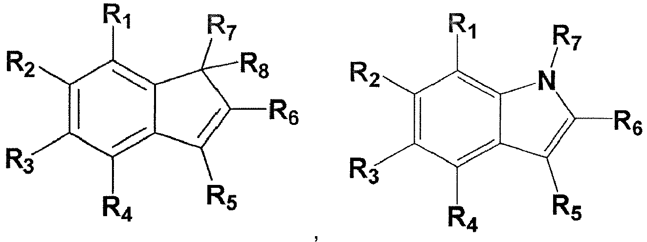
- In addition, in the present specification, the expression 'neighboring groups may be linked to each other to form a ring' is used in the same sense as 'neighboring groups are linked selectively to each other to form a ring', and a case where at least one pair of neighboring groups may be bonded to each other to form a ring.
- Hereinafter, referring to
Figures 1 to 3 , a lamination structure of an organic electric element including the compound of the present invention will be described. - In designation of reference numerals to components in respective drawings, it should be noted that the same elements will be designated by the same reference numerals although they are shown in different drawings. In addition, in the following description of the present invention, a detailed description of known functions and configurations incorporated herein will be omitted when it may make the subject matter of the present invention rather unclear.
- In addition, terms, such as first, second, A, B, (a), (b) or the like may be used herein when describing components of the present invention. Each of these terminologies is not used for defining an essence, order or sequence of a corresponding component but used merely to distinguish the corresponding component from other component(s). It will be understood that the expression "one component is "connected," "coupled" or "joined" to another component" comprises the case where a third component may be "connected," "coupled," and "joined" between the first and second components as well as the case where the first component may be directly connected, coupled or joined to the second component.
- In addition, it will be understood that when an element such as a layer, film, region or substrate is referred to as being "on" or "over" another element, it can be directly on the other element or intervening elements may also be present. In contrast, when an element is referred to as being "directly on" another element, there are no intervening elements present.
- The
Figures 1 to 3 are laminated structures for showing an example of an organic electric element according to an embodiment of the present invention, respectively. - Referring to the
FIG. 1 , an organicelectric element 100 according to an embodiment of the present invention includes afirst electrode 110 formed on a substrate (not shown), asecond electrode 170, and an organic material layer formed between thefirst electrode 110 and thesecond electrode 170. - The
first electrode 110 may be an anode (positive electrode), and thesecond electrode 170 may be a cathode (negative electrode). In the case of an inverted organic electric element, the first electrode may be a cathode, and the second electrode may be an anode. - The organic material layer may be comprised a
hole injection layer 120, ahole transport layer 130, alight emitting layer 140, anelectron transport layer 150, and anelectron injection layer 160. Specifically, ahole injection layer 120, ahole transport layer 130, alight emitting layer 140, anelectron transport layer 150, and anelectron injection layer 160 are formed on thefirst electrode 110 in sequence. - Preferably, a layer for improving the
luminous efficiency 180 may be formed one side of sides of thefirst electrode 110 and thesecond electrode 170, wherein one side is not facing the organic material layer, as a result the luminous efficiency of an organic electric element can be improved. - For example, the light
efficiency improving layer 180 may be formed on thesecond electrode 170, as a result, in the case of a top emission organic light emitting diode, the optical energy loss due to Surface Plasmon Polaritons (SPPs) at thesecond electrode 170 may be reduced and in the case of a bottom emission organic light emitting diode, the lightefficiency improving layer 180 may serve as a buffer for thesecond electrode 170. - Meanwhile, a
buffer layer 210 or an emission-auxiliary layer 220 may be further formed between thehole transport layer 130 and thelight emitting layer 140, which will be described with reference toFIG. 2 . - Referring to
FIG. 2 , the organicelectric element 200 according to another embodiment of the present invention may comprise ahole injection layer 120, ahole transport layer 130, abuffer layer 210, an emission-auxiliary layer 220, alight emitting layer 140, theelectron transport layer 150, theelectron injection layer 160, and asecond electrode 170 formed on afirst electrode 110 in sequence, and a lightefficiency improving layer 180 may be formed on thesecond electrode 170. - Although not shown in
FIG. 2 , an electron transport auxiliary layer may be further formed between the light emittinglayer 140 and theelectron transport layer 150. - In addition, according to another embodiment of the present invention, the organic material layer may be a form consisting of a plurality of stacks, wherein the stacks comprise a hole transport layer, a light emitting layer, and an electron transport layer, respectively. This will be described with reference to
FIG. 3 . - Referring to
FIG. 3 , two or more sets of stacks of the organic material layers ST1 and ST2 may be formed between thefirst electrode 110 and thesecond electrode 170 in the organicelectric element 300 according to another embodiment of the present invention, wherein the organic material layers are consisted of multiple layers, respectively, and the charge generation layer CGL may be formed between the stacks of the organic material layer. - Specifically, the organic electric element according to the embodiment of the present invention may comprise the
first electrode 110, the first stack ST1, the charge generation layer CGL, the second stack ST2, and thesecond electrode 170 and the lightefficiency improving layer 180. - The first stack ST1 is an organic layer formed on the
first electrode 110, and the first stack ST1 may comprise the firsthole injection layer 320, the firsthole transport layer 330, the firstlight emitting layer 340 and the firstelectron transport layer 350 and the second stack ST2 may comprise a secondhole injection layer 420, a secondhole transport layer 430, a secondlight emitting layer 440 and a secondelectron transport layer 450. As such, the first stack and the second stack may be the organic layers having the same or different stacked structures. - The charge generation layer CGL may be formed between the first stack ST1 and the second stack ST2. The charge generation layer CGL may comprise a first
charge generation layer 360 and a secondcharge generation layer 361. The charge generating layer CGL is formed between the firstlight emitting layer 340 and the secondlight emitting layer 440 to increase the current efficiency generated in each light emitting layer and to smoothly distribute charges. - The first
light emitting layer 340 may comprise a light emitting material comprising a blue host doped with a blue fluorescent dopant and the secondlight emitting layer 440 may comprise a light emitting material comprising a green host doped with a greenish yellow dopant and a red dopant together, but the material of the firstlight emitting layer 340 and the secondlight emitting layer 440 according to an embodiment of the present invention is not limited thereto. - In
FIG. 3 , n may be an integer of 1 to 5 and the charge generation layer CGL and the third stack may be further stacked on the second stack ST2 when n is 2. - When a plurality of light emitting layers are formed in a multi-layer stack structure as shown in
FIG. 3 , it is possible to manufacture an organic electroluminescent element that emits not only white light but also various colors, wherein the white light is emitted by the mixing effect of light emitted from each light emitting layer. - The mixture of the compound represented by Formula 1 can be used as material of a
hole injection layer hole transport layer buffer layer 210, an emission-auxiliary layer 220, anelectron transport layer electron injection layer 160, alight emitting layer luminous efficiency 180, preferably as material of an emission-auxiliary layer 220 and/or a layer for improvingluminous efficiency 180. - Even if the core is the same core, the band gap, the electrical characteristics, the interface characteristics and the like may be different depending on which substituent is bonded at which position. Therefore, it is necessary to study the selection of the core and the combination of the core and the sub-substituent bonded to the core. In particular, long life span and high efficiency can be simultaneously achieved when the optimal combination of energy levels and T1 values, inherent material properties (mobility, interfacial properties, etc.), and the like among the respective layers of an organic material layer is achieved.
- Therefore, energy level and T1 value between the respective layers of the organic material layer, inherent material properties (mobility, interfacial properties, etc.) and the like can be optimized by using the mixture of the compound represented by Formula 1 as an emission-
auxiliary layer 220 and/or a layer for improvingluminous efficiency 180, and thus it is possible to simultaneously improve the lifetime and efficiency of the organic electric element. - The organic electric element according to an embodiment of the present invention may be manufactured using various deposition methods. The organic electric element according to an embodiment of the present invention may be manufactured using a PVD (physical vapor deposition) method or CVD (chemical vapor deposition) method. For example, the organic electric element may be manufactured by depositing a metal, a conductive metal oxide, or a mixture thereof on the substrate to form the
anode 110, forming the organic material layer comprising thehole injection layer 120, thehole transport layer 130, thelight emitting layer 140, theelectron transport layer 150, and theelectron injection layer 160 thereon, and then depositing a material, which can be used as thecathode 170, thereon. Also, an emission-auxiliary layer 220 may be formed between ahole transport layer 130 and alight emitting layer 140, and an electron transport auxiliary layer(not shown) may be further formed between a light emittinglayer 140 and anelectron transport layer 150 and, as described above, a stack structure may be formed. - Also, the organic material layer may be manufactured in such a manner that the fewer layers are formed using various polymer materials by a soluble process or solvent process, for example, spin coating, nozzle printing, inkjet printing, slot coating, dip coating, roll-to-roll, doctor blading, screen printing, or thermal transfer, instead of deposition. Since the organic material layer according to the present invention may be formed in various ways, the scope of protection of the present invention is not limited by a method of forming the organic material layer.
- The organic electric element according to an embodiment of the present invention may be of a top emission type, a bottom emission type, or a dual emission type depending on the material used.
- In addition, the organic electric element according to an embodiment of the present invention may be selected from the group consisting of an organic light emitting diode, an organic solar cell, an organic photo conductor, an organic transistor, an element for monochromatic illumination and an element for quantum dot display.
- Another embodiment of the present invention provides an electronic device including a display device which includes the above described organic electric element, and a control unit for controlling the display device. Here, the electronic device may be a wired/wireless communication terminal which is currently used or will be used in the future, and covers all kinds of electronic devices including a mobile communication terminal such as a cellular phone, a personal digital assistant (PDA), an electronic dictionary, a point-to-multipoint (PMP), a remote controller, a navigation unit, a game player, various kinds of TVs, and various kinds of computers.
- Hereinafter, the compound according to an aspect of the present invention will be described.
- The compound according to an aspect of the present invention is represented by formula 1 below.

- In Formula 1, each of symbols may be defined as follows.
- x and y are each an integer of 0 to 2, preferably, an integer of 0 or 1, and x+y is an integer greater than or equal to 1. Where x and y are each 2, each of L2s, each of L3s, each of Ar3s, each of Ar4s, each of Ar5s, each of Ar6s is the same or different from each other.
- Ar1 to Ar6 are each independently selected from the group consisting of a C6-C60 aryl group, a fluorenyl group, a C2-C60 heterocyclic group containing at least one heteroatom of O, N, S, Si, and P, a C3-C60 aliphatic ring group, -L'-N(Ra)(Rb), Formula A-1 and Formula A-2, and at least one of Ar1 to Ar6 is Formula A-1 or Formula A-2,
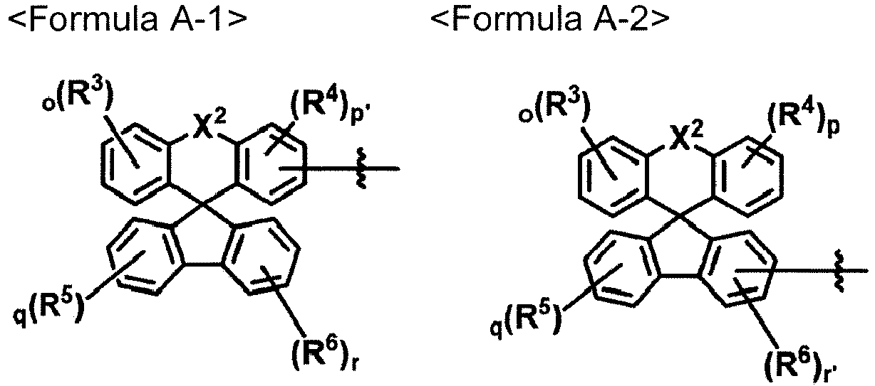
- X1 is O or S and X2 is N(R'), O or S.
- Where at least one of Ar1 to Ar6 is an aryl group, the aryl group may be preferably a C6-C30, more preferably a C6-C18 aryl group, for example, phenyl, biphenyl, naphthyl, terphenyl and the like.
- Where at least one of Ar1 to Ar6 is a heterocyclic group except for Formula A-1 or Formula A-2, the heterocyclic group may be preferably a C2-C30, more preferably a C2-C16 heterocyclic group, for example, dibenzofuran, dibenzothiophene, naphthobenzofuran, naphthobenzothiophene and the like.
- Where at least one of Ar1 to Ar6 is a fluorenyl group, the fluorenyl group may be 9,9-dimethyl-9H-fluorene, 9,9-diphenyl-9H-fluorene, 9,9'-spirofluorene and the like.
- R1 to R6 are each independently selected from the group consisting of hydrogen, deuterium, halogen, cyano group, nitro group, a C6-C60 aryl group, a fluorenyl group, a C2-C60 heterocyclic group containing at least one heteroatom of O, N, S, Si, and P, a C3-C60 aliphatic ring group, a C1-C30 alkyl group, a C2-C30 alkenyl group, a C2-C30 alkynyl group, a C1-C30 alkoxyl group, a C6-C30 aryloxy group and -L'-N(Ra)(Rb), and adjacent groups together may be bonded to each other to form a ring.
- Here, the term 'neighboring groups' means neighboring R1s, neighboring R2s, neighboring R3s, neighboring R4s, neighboring R5s, neighboring R6s, neighboring R3 and R', and/or neighboring R4 and R'.
- The ring formed by bonding between neighboring R1s, neighboring R2s, neighboring R3s, neighboring R4s, neighboring R5s or/and neighboring R6s is/are a C6-C60 aromatic ring group, a fluorenyl group, a C2-C60 heterocyclic group containing at least one heteroatom of O, N, S, Si and P, or a C3-C60 aliphatic ring. For example, where the aromatic ring is formed by bonding between neighboring groups, the aromatic ring may be preferably a C6-C20 aromatic ring group, more preferably, a C6-C14 aromatic ring group, for example, benzene, naphthalene, phenanthrene or the like.
- Where neighboring R3 and R', and/or neighboring R4 and R' are bonded to each other to form a ring, as a result, a heterocyclic ring containing N may be formed, wherein the heterocyclic ring is the compound comprising moiety such as indole, carbazole, phenothiazine, phenoxazine, acridine or the like.
- n, p' and r' are each an integer of 0 to 3, m, o, p, q and r are each an integer of 0 to 4, where they are each an integer of 2 or more, each of R1s, each of R2s, each of R3s, each of R4s, each of R5s, each of R6s is the same or different from each other.
- Where at least one of R1 to R6 is an aryl group, the aryl group may be preferably a C6-C30, more preferably a C6-C18 aryl group, for example, phenyl, biphenyl, naphthyl, terphenyl and the like.
- Where at least one of R1 to R6 is a heterocyclic group, the heterocyclic group may be preferably a C2-C30, more preferably a C2-C18 heterocyclic group, for example, dibenzothiophene, dibenzofuran, carbazole, phenylcarbazole and the like.
- Where at least one of R1 to R6 is an alkyl group, the alkyl group may be preferably a C1-C10 alkyl group, for example, methyl, t-butyl and the like.
- Where at least one of R1 to R6 is an alkoxyl group, the alkoxyl group may be preferably a C1-C20 alkoxy group, more preferably a C1-C10 alkoxy group, for example, methoxy, t-butoxy and the like.
- L1 to L3 and L' are each independently selected from the group consisting of a single bond, a C6-C60 arylene group, a fluorenylene group, a C3-C60 aliphatic ring group and a C2-C60 heterocyclic group containing at least one heteroatom of O, N, S, Si, and P.
- Where at least one of L1 to L3 and L' is an arylene group, the arylene group may be preferably a C6-C30, more preferably a C6-C18 arylene group, for example, phenylene, naphthalene, biphenyl, terphenyl and the like.
- R', Ra and Rb are each independently selected from the group consisting of a C6-C60 aryl group, a fluorenyl group, a C2-C60 heterocyclic group containing at least one heteroatom of O, N, S, Si, and P and a C3-C60 aliphatic ring group.
- Where at least one of R', Ra and Rb is an aryl group, the aryl group may be preferably a C6-C30, more preferably a C6-C18 aryl group, for example, phenyl, biphenyl, naphthyl, terphenyl, phenanthrene and the like.
- Where at least one of R', Ra and Rb is a heterocyclic group, the heterocyclic group may be preferably a C2-C30, more preferably a C2-C18 heterocyclic group, for example, carbazole, phenylcarbazole, dibenzofuran, dibenzothiophene and the like.
- Where at least one of R', Ra and Rb is a fluorenyl group, the fluorenyl group may be 9,9-dimethyl-9H-fluorene, 9,9-diphenyl-9H-fluorene, 9,9'-spirofluorene and the like.
- Ar1 to Ar6, R1 to R6, L1 to L3, R' and the ring formed by adjacent groups may be each optionally substituted with one or more substituents selected from the group consisting of deuterium, halogen, a silane group unsubstituted or substituted with a C1-C20 alkyl group or a C6-C20 aryl group, a siloxane group, a boron group, a germanium group, a cyano group, a nitro group, a C1-C20 alkylthio group, a C1-C20 alkoxy group, a C6-C20 aryloxy group, a C6-C20 arylthio group, a C1-C20 alkyl group, a C2-C20 alkenyl group, a C2-C20 alkynyl group, a C6-C20 aryl group, a fluorenyl group, a C2-C20 heterocyclic group containing at least one heteroatom of O, N, S, Si, and P, a C3-C20 aliphatic ring group, a C7-C20 arylalkyl group, and C8-C20 arylalkenyl group.
- Formula 1 may be represented by Formula 2 or Formula 3.

- In Formulas 2 and 3, X1, L1-L3, Ar1-Ar6, R1, R2, n, m are the same as defined for Formula 1.
- In addition, Formula 1 may be represented by one of Formula 4 to Formula 19.


- In Formulas 4 to 19, X1, L1-L3, Ar1-Ar6, R1, R2, n, m are the same as defined for Formula 1.
- In addition, Formula 1 may be represented by one of Formula 20 to Formula 34.


- In Formulas 20 to 34, X1, L1-L3, Ar1-Ar6, R1, R2, n, m are the same as defined for Formula 1, and a and b are each an integer of 0 to 6.
- Specifically, the compound represented by formula 1 may be one of the following compounds, but there is no limitation thereto.


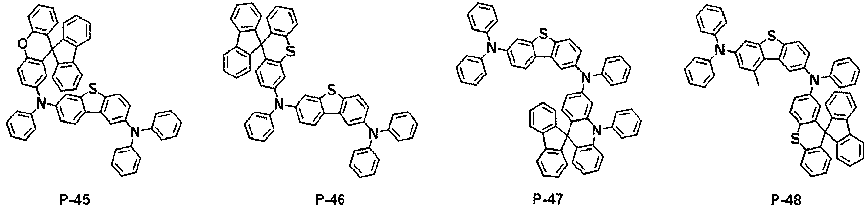


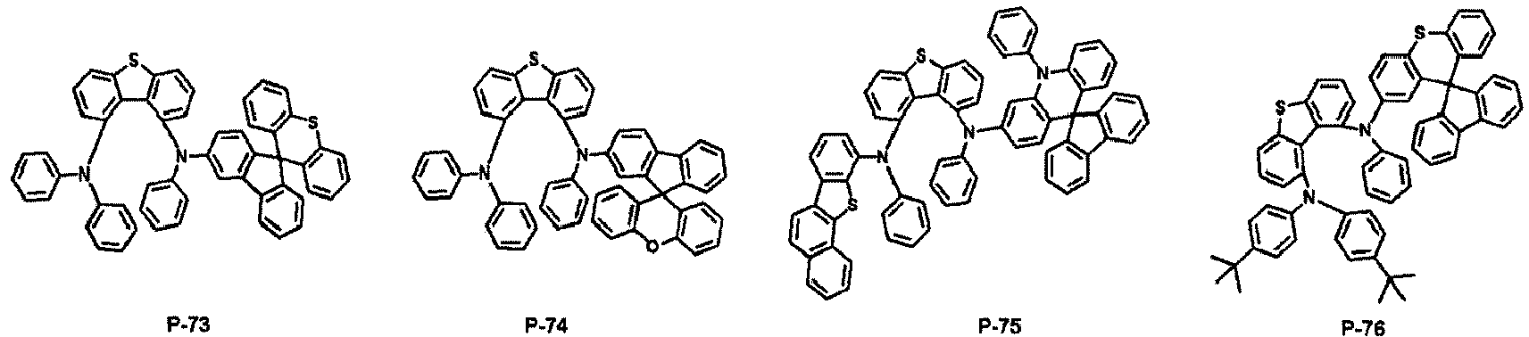


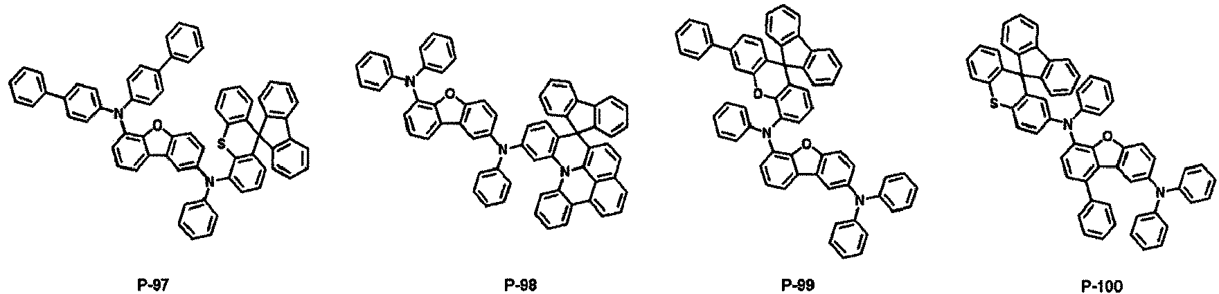


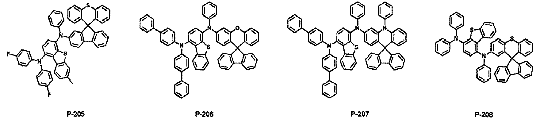


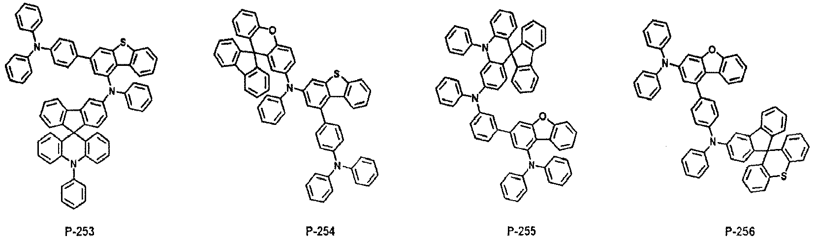


- In another aspect of the present invention, the present invention provides an organic electric element comprising an anode, a cathode, and an organic material layer formed between the anode and the cathode, wherein the organic material layer comprises a single compound or two or more compounds represented by Formula 1.
- In another aspect of the present invention, the present invention provides an organic electric element comprising an anode, a cathode, an organic material layer formed between the anode and the cathode, and a layer for improving luminous efficiency. Here, the layer for improving luminous efficiency is formed on one side of the anode or the cathode, the one side is not facing the organic material layer and the layer for improving luminous efficiency comprises compound represented by Formula 1.
- The organic material layer comprises at least one of a hole injection layer, a hole transport layer, an emission-auxiliary layer, a light emitting layer, an electron transport-auxiliary layer, an electron transport layer and an electron injection layer, preferably, the compound may be comprised in the emission-auxiliary layer.
- The organic material layer may comprise two or more stacks, wherein the stacks may comprise a hole transport layer, a light emitting layer, and an electron transport layer formed in sequence on the anode, and a charge generation layer may be formed between the two or more stacks.
- In another aspect of the present invention, the present invention provides an electronic device comprising a display device and a control unit for controlling the display device, wherein the display device comprises the organic electric element comprising compound represented by Formula 1.
- Hereinafter, synthesis example of the compound represented by Formula 1 and preparation method of an organic electroluminescent element according to the present invention will be described in detail by way of examples. However, the present invention is not limited to the following examples.
- The compound (final product) represented by Formula 1 according to the present invention can be synthesized according to the reaction route of the following Reaction Scheme 1, but there is no limitation thereto.


- Sub 1 of the Reaction Scheme 1 can be synthesized according to the reaction route of the following Reaction Scheme 2-1 or 2-2, but there is no limitation thereto. Sub 1 can be synthesized according to the reaction route of the following Reaction Scheme 2-1 where X1 is S and according to the reaction route of the following Reaction Scheme 2-2 where X1 is O.


-

- (3-chlorophenyl)boronic acid (50.0 g, 320 mmol) was dissolved in THF (1.6 L), (2-bromo-6-iodophenyl)(ethyl)sulfane (110 g, 320 mmol), NaOH (38.4 g, 959 mmol), Pd(PPh3)4 (22.2 g, 19.2 mmol) and water (800 mL) were added thereto and the mixture was stirred at 80°C. When the reaction was completed, the reaction product was extracted with CH2Cl2 and water, and then the organic layer was dried with MgSO4 and concentrated. Then, the concentrate was separated through a silica gel column and recrystallized to obtain 88.0 g (yield: 84%) of the product.
- Acetic acid (1.1 L) and 35% Hydrogen peroxide (H2O2) (76.7 mL) were added to Sub1-1-a (88.0 g, 269 mmol) and the mixture was stirred at room temperature. When the reaction was completed, the reaction product was neutralized with an aqueous NaOH solution and extracted with EA (ethylacetate) and water. Thereafter, the organic layer was dried with MgSO4 and concentrated. Then, the concentrate was separated through a silica gel column and recrystallized to obtain 82.2 g (yield: 89%) of the product.
- After adding Sub1-1-b (82.2 g, 239 mmol) to an excess of trifluoromethane-sulfonic acid, the mixture was stirred at room temperature for 24 hours Thereafter, water and pyridine (8:1) were slowly added thereto and the mixture was refluxed for 30 minutes. The reaction product was cooled down and extracted with CH2Cl2 and water. Thereafter, the organic layer was dried with MgSO4 and concentrated. Then, the concentrate was separated through a silica gel column and recrystallized to obtain Sub1-1 28.5 g (yield: 40%) and Sub1-7 29.9 g (yield: 42%) of the products.
-

- The reaction was carried out in the same manner as in the synthesis method of Sub1-1-a using (4-chlorophenyl) boronic acid (20.0 g, 128 mmol), THF, (4-bromo-2-iodophenyl)(ethyl)sulfane (43.9 g, 128 mmol), NaOH (15.4 g, 384 mmol), Pd(PPh3)4 (8.87 g, 7.67 mmol) and water to obtain 33.9 g (yield: 81%) of product.
- The reaction was carried out in the same manner as in the synthesis method of Sub1-1-b using Sub1-13-a (33.9 g, 104 mmol), acetic acid (414 mL) and 35% Hydrogen peroxide (H2O2) (29.6 mL) to obtain 32.8 g (yield: 92%) of product.
- The reaction was carried out in the same manner as in the synthesis method of Sub1-1 using Sub1-13-b (32.8 g, 95.3 mmol) instead of Sub1-1-b to obtain 23.8 g (yield: 84%) of the product.
-

- The reaction was carried out in the same manner as in the synthesis method of Sub1-1-a using (4-chlorophenyl) boronic acid (20.0 g, 128 mmol), 4-bromo-2-iodophenol (38.2 g, 128 mmol), NaOH (15.3 g, 384 mmol), Pd(PPh3)4 (8.87 g, 7.67 mmol) to obtain 29.7 g (yield: 82%) of product.
- Pd(OAc)2 (1.18 g, 5.24 mmol), 3-nitropyridine (0.65 g, 5.24 mmol), BzOOt-Bu (tert-butyl peroxybenzoate) (40.7 g, 210 mmol), C6F6 (hexafluorobenzene) (160 mL), DMI (N,N'-dimethylimidazolidinone) (105 mL) were added to Sub1-35-c (29.7 g, 105 mmol) and the mixture was refluxed at 90°C for 3 hours. When the reaction was completed, the reaction product was cooled to room temperature, and extracted with EA and water. The organic layer was dried with MgSO4 and concentrated. Thereafter, the concentrate was separated by a silica gel column and recrystallized to obtain 19.2 g (yield: 65%) of the product.
-

- The reaction was carried out in the same manner as in the synthesis method of Sub1-1-a using (2-chlorophenyl) boronic acid (20.0 g, 128 mmol), 4-bromo-2-iodophenol (38.2 g, 128 mmol), NaOH (15.3 g, 384 mmol), Pd(PPh3)4 (8.87 g, 7.67 mmol) to obtain 29.0 g (yield: 80%) of product.
- The reaction was carried out in the same manner as in the synthesis method of Sub1-1-a using Sub1-40-c (29.0 g, 102 mmol), Pd(OAc)2 (1.15 g, 5.12 mmol), 3-nitropyridine (0.64 g, 5.12 mmol), BzOOt-Bu (tert-butyl peroxybenzoate) (39.7 g, 205 mmol), C6F6 (hexafluorobenzene) (150 mL), DMI (N,N'-dimethylimidazolidinone) (100 mL) were added to Sub1-40-c (29.0 g, 102 mmol) to obtain 17.9 g (yield 62%) of product.
-

- The reaction was carried out in the same manner as in the synthesis method of Sub1-1-a using (3-chloronaphthalen-2-yl) boronic acid (20.0 g, 96.9 mmol), (5-bromo-2-iodophenyl)(ethyl)sulfane (33.2 g, 96.9 mmol), NaOH (11.6 g, 291 mmol), Pd(PPh3)4 (6.72 g, 5.81 mmol) to obtain 31.5 g (yield: 86%) of product.
- The reaction was carried out in the same manner as in the synthesis method of Sub1-1-b using Sub1-46-a (31.5 g, 83.3 mmol), acetic acid (333 mL), 35% Hydrogen peroxide (H2O2) (23.8 mL) to obtain 28.5 g (yield: 87%) of product.
- The reaction was carried out in the same manner as in the synthesis method of Sub1-1 using Sub1-1-46-b (28.5 g, 72.5 mmol) to obtain 20.9 g (yield: 83%) of product.
-

- The reaction was carried out in the same manner as in the synthesis method of Sub1-1-a using (1-chloronaphthalen-2-yl) boronic acid (20.0 g, 96.9 mmol), (4'-bromo-4-iodo-[1,1'-biphenyl]-3-yl)(ethyl)sulfane (40.6 g, 96.9 mmol), NaOH (11.6 g, 291 mmol), Pd(PPh3)4 (6.72 g, 5.81 mmol) to obtain 35.6 g (yield: 81%) of product.
- The reaction was carried out in the same manner as in the synthesis method of Sub1-1-b using Sub1-88-a (35.6 g, 78.5 mmol), acetic acid (314 mL), 35% Hydrogen peroxide (H2O2) (22.4 mL) to obtain 34.3 g (yield: 93%) of product.
- The reaction was carried out in the same manner as in the synthesis method of Sub1-1 using Sub1-1-88-b (34.3 g, 73.0 mmol) instead of Sub1-1-b to obtain 23.8 g (yield: 77%) of the product.
-

- The reaction was carried out in the same manner as in the synthesis method of Sub1-1-a using Phenylboronic acid (20.0 g, 164 mmol), 5-bromo-3-iodo-2-(methylthio)phenol (56.6 g, 164 mmol), NaOH (19.7 g, 492 mmol), Pd(PPh3)4 (11.4 g, 9.84 mmol) to obtain 41.2 g (yield: 85%) of product.
- The reaction was carried out in the same manner as in the synthesis method of Sub1-1-b using Sub1-90-a (41.2 g, 139 mmol), acetic acid (40 mL), 35% Hydrogen peroxide (H2O2) (560 mL) to obtain 40.8 g (yield: 94%) of product.
- The reaction was carried out in the same manner as in the synthesis method of Sub1-1 using Sub1-1-90-b (40.8 g, 131 mmol) to obtain 28.9 g (yield: 79%) of product.
-

- The reaction was carried out in the same manner as in the synthesis method of Sub1-1-a using (5-bromo-2-chlorophenyl) boronic acid (30.0 g, 128 mmol), (2-iodophenyl)(methyl)sulfane (31.9 g, 128 mmol), NaOH (15.3 g, 383 mmol), Pd(PPh3)4 (8.84 g, 7.65 mmol) to obtain 32.8 g (yield: 82%) of product.
- The reaction was carried out in the same manner as in the synthesis method of Sub1-1-b using Sub1-92-a (32.8 g, 105 mmol), acetic acid (30 mL), 35% Hydrogen peroxide (H2O2) (420 mL) to obtain 33.1 g (yield: 96%) of product.
- The reaction was carried out in the same manner as in the synthesis method of Sub1-1 using Sub1-1-92-b (33.1 g, 100 mmol) to obtain 21.5 g (yield: 72%) of product.
-

- The reaction was carried out in the same manner as in the synthesis method of Sub1-1-a using (2-bromo-4-chlorophenyl) boronic acid (30.0 g, 128 mmol), (2-iodophenyl)(methyl)sulfane (31.9 g, 128 mmol), NaOH (15.3 g, 383 mmol), Pd(PPh3)4 (8.84 g, 7.65 mmol) to obtain 32.4 g (yield: 81%) of product.
- The reaction was carried out in the same manner as in the synthesis method of Sub1-1-b using Sub1-96-a (32.4 g, 103 mmol), acetic acid (30 mL), 35% Hydrogen peroxide (H2O2) (420 mL) to obtain 32.0 g (yield: 94%) of product.
- The reaction was carried out in the same manner as in the synthesis method of Sub1-1 using Sub1-1-96-b (32.0 g, 97.1 mmol) to obtain 22.0 g (yield: 76%) of product.
-

- The reaction was carried out in the same manner as in the synthesis method of Sub1-1-a using (2-chlorophenyl) boronic acid (20.0 g, 164 mmol), 4-bromo-2-iodophenol (54.7 g, 164 mmol), NaOH (19.7 g, 492 mmol), Pd(PPh3)4 (11.4 g, 9.84 mmol) to obtain 40.0 g (yield: 86%) of product.
- The reaction was carried out in the same manner as in the synthesis method of Sub1-35 using Sub1-102-c (40.0 g, 141 mmol), Pd(OAc)2 (1.58 g, 7.05 mmol), 3-nitropyridine (0.88 g, 7.05 mmol), BzOOt-Bu (tert-butyl peroxybenzoate) (54.8 g, 282 mmol), C6F6 (hexafluorobenzene) (210 mL), DMI (N,N'-dimethylimidazolidinone) (140 mL) to obtain 25.0 g (yield 63%) of product.
-

- The reaction was carried out in the same manner as in the synthesis method of Sub1-1-a using Phenylboronic acid (20.0 g, 164 mmol), 3-bromo-4-chloro-2-iodophenol (54.7 g, 164 mmol), NaOH (19.7 g, 492 mmol), Pd(PPh3)4 (11.4 g, 9.84 mmol) to obtain 38.6 g (yield: 83%) of product.
- The reaction was carried out in the same manner as in the synthesis method of Sub1-35 using Sub1-106-c (38.6 g, 136 mmol), Pd(OAc)2 (1.53 g, 6.81 mmol), 3-nitropyridine (0.85 g, 6.81 mmol), BzOOt-Bu (tert-butyl peroxybenzoate) (52.9 g, 272 mmol), C6F6 (hexafluorobenzene) (200 mL), DMI (N,N'-dimethylimidazolidinone) (140 mL) to obtain 24.9 g (yield 65%) of product.
- The compounds belonging to Sub 1 may be, but not limited to, the following compounds, and Table 1 shows FD-MS(Field Desorption-Mass Spectrometry) values of the following compounds.





[Table 1] Compound FD-MS Compound FD-MS Sub 1-1 m/z=295.91(C12H6BrClS=297.59) Sub 1-2 m/z=295.91(C12H6BrClS=297.59) Sub 1-3 m/z=537.00(C30H17BrClNS=538.89) Sub 1-4 m/z=309.92(C13H8BrClS=311.62) Sub 1-5 m/z=313.90(C12H5BrClFS=315.58) Sub 1-6 m/z=371.94(C18H10BrClS=373.69) Sub 1-7 m/z=295.91(C12H6BrClS=297.59) Sub 1-8 m/z=309.92(C13H8BrClS=311.62) Sub 1-9 m/z=295.91(C12H6BrClS=297.59) Sub 1-10 m/z=461.95(C24H12BrClOS=463.77) Sub 1-11 m/z=295.91(C12H8BrClS=297.59) Sub 1-12 m/z=309.92(C13H8BrClS=311.62) Sub 1-13 m/z=295.91(C12H6BrClS=297.59) Sub 1-14 m/z=309.92(C13H8BrClS=311.62) Sub 1-15 m/z=295.91(C12H6BrClS=297.59) Sub 1-16 m/z=295.91(C12H6BrClS=297.59) Sub 1-17 m/z=295.91(C12H6BrClS=297.59) Sub 1-18 m/z=295.91(C12H6BrClS=297.59) Sub 1-19 m/z=279.93(C12H6BrClO=281.53) Sub 1-20 m/z=355.96(C18H10BrClO=357.63) Sub 1-21 m/z=304.92(C13H5BrClNO=306.54) Sub 1-22 m/z=309.94(C13H8BrClO2=311.56) Sub 1-23 m/z=297.92(C12H5BrClFO=299.52) Sub 1-24 m/z=279.93(C12H6BrClO=281.53) Sub 1-25 m/z=297.92(C12H5BrClFO=299.52) Sub 1-26 m/z=293.94(C13H8BrClO=295.56) Sub 1-27 m/z=279.93(C12H6BrClO=281.53) Sub 1-28 m/z=309.94(C13H8BrClO2=311.56) Sub 1-29 m/z=355.96(C18H10BrClO=357.63) Sub 1-30 m/z=279.93(C12H6BrClO=281.53) Sub 1-31 m/z=304.92(C13H5BrClNO=306.54) Sub 1-32 m/z=279.93(C12H6BrClO=281.53) Sub 1-33 m/z=297.92(C12H5BrClFO=299.52) Sub 1-34 m/z=304.92(C13H5BrClNO=306.54) Sub 1-35 m/z=279.93(C12H6BrClO=281.53) Sub 1-36 m/z=293.94(C13H8BrClO=295.56) Sub 1-37 m/z=279.93(C12H6BrClO=281.53) Sub 1-38 m/z=297.92(C12H5BrClFO=299.52) Sub 1-39 m/z=279.93(C12H6BrClO=281.53) Sub 1-40 m/z=279.93(C12H6BrClO=281.53) Sub 1-41 m/z=355.96(C18H10BrClO=357.63) Sub 1-42 m/z=279.93(C12H6BrClO=281.53) Sub 1-43 m/z=345.92(C16H8BrClS=347.65) Sub 1-44 m/z=329.94(C16H8BrClO=331.59) Sub 1-45 m/z=329.94(C16H8BrClO=331.59) Sub 1-46 m/z=329.94(C16H8BrClO=331.59) Sub 1-47 m/z=345.92(C16H8BrClS=347.65) Sub 1-48 m/z=345.92(C16H8BrClS=347.65) Sub 1-49 m/z=329.94(C16HaBrClO=331.59) Sub 1-50 m/z=329.94(C16H8BrClO=331.59) Sub 1-51 m/z=345.92(C16H8BrClS=347.65) Sub 1-52 m/z=345.92(C16H8BrClS=347.65) Sub 1-53 m/z=329.94(C16H8BrClO=331.59) Sub 1-54 m/z=329.94(C16H8BrClO=331.59) Sub 1-55 m/z=395.94(C20H10BrClS=397.71) Sub 1-56 m/z=395.94(C20H10BrClS=397.71) Sub 1-57 m/z=379.96(C20H10BrClO=381.65) Sub 1-58 m/z=379.96(C20H10BrClO=381.65) Sub 1-59 m/z=395.94(C20H10BrClS=397.71) Sub 1-60 m/z=395.94(C20H10BrClS=397.71) Sub 1-61 m/z=379.96(C20H10BrClO=381.65) Sub 1-62 m/z=379.96(C20H10BrClO=381.65) Sub 1-63 m/z=395.94(C20H10BrClS=397.71) Sub 1-64 m/z=395.94(C20H10BrClS=397.71) Sub 1-65 m/z=379.96(C20H10BrClO=381.65) Sub 1-66 m/z=379.96(C20H10BrClO=381.65) Sub 1-67 m/z=395.94(C20H10BrClS=397.71) Sub 1-68 m/z=395.94(C20H10BrClS=397.71) Sub 1-69 m/z=379.96(C20H10BrClO=381.65) Sub 1-70 m/z=379.96(C20H10BrClO=381.65) Sub 1-71 m/z=395.94(C20H10BrClS=397.71) Sub 1-72 m/z=395.94(C20H10BrClS=397.71) Sub 1-73 m/z=379.96(C20H10BrClO=381.65) Sub 1-74 m/z=379.96(C20H10BrClO=381.65) Sub 1-75 m/z=395.94(C20H10BrClS=397.71) Sub 1-76 m/z=395.94(C20H10BrClS=397.71) Sub 1-77 m/z=379.96(C20H10BrClO=381.65) Sub 1-78 m/z=379.96(C20H10BrClO=381.65) Sub 1-79 m/z=371.94(C18H10BrClS=373.69) Sub 1-80 m/z=405.98(C22H12BrClO=407.69) Sub 1-81 m/z=355.96(C18H10BrClO=357.63) Sub 1-82 m/z=371.94(C18H10BrClS=373.69) Sub 1-83 m/z=421.95(C22H12BrClS=423.75) Sub 1-84 m/z=477.93(C24H12BrClS2=479.83) Sub 1-85 m/z=355.96(C18H10BrClO=357.63) Sub 1-86 m/z=371.99(C19H14BrClO=373.67) Sub 1-87 m/z=421.95(C22H12BrClS=423.75) Sub 1-88 m/z=421.95(C22H12BrClS=423.75) Sub 1-89 m/z=310.00(C14H15BrOS=311.24) Sub 1-90 m/z=310.00(C14H15BrOS=311.24) Sub 1-91 m/z=492.02(C26H21BrOS2=493.48) Sub 1-92 m/z=327.97(C14H14BrClS=329.68) Sub 1-93 m/z=341.98(C15H16BrClS=343.71) Sub 1-94 m/z=386.03(C20H19BrOS=387.34) Sub 1-95 m/z=293.97(C13H11BrOS=295.19) Sub 1-96 m/z=311.94(C13H10BrClS=313.64) Sub 1-97 m/z=336.93(C14H9BrClNS=338.65) Sub 1-98 m/z=327.97(C14H14BrClS=329.68) Sub 1-99 m/z=311.99(C14H14BrClO=313.62) Sub 1-100 m/z=342.00(C15H16BrClO2=343.65) Sub 1-101 m/z=311.99(C14H14BrClO=313.62) Sub 1-102 m/z=311.99(C14H14BrClO=313.62) Sub 1-103 m/z=295.96(C13H10BrClO=297.58) Sub 1-104 m/z=313.95(C13H9BrClFO=315.57) Sub 1-105 m/z=295.96(C13H10BrClO=297.58) Sub 1-106 m/z=311.99(C14H14BrClO=313.62) Sub 1-107 m/z=343.96(C14H14BrClOS=345.68) Sub 1-108 m/z=311.96(C13H10BrClO2=313.58) Sub 1-109 m/z=360.02(C18H17BrOS=361.30) Sub 1-110 m/z=362.01(C18H16BrClO=363.68) Sub 1-111 m/z=345.98(C17H12BrClO=347.64) Sub 1-112 m/z=361.95(C17H12BrClS=363.70) Sub 1-113 m/z=361.95(C17H12BrClS=363.70) Sub 1-114 m/z=362.01(C18H16BrClO=363.68) - Sub 2 of Reaction Scheme 1 can be synthesized by the reaction route of of the following Reaction Scheme 3(disclosed in Korean Patent Registration No.
10-1251451 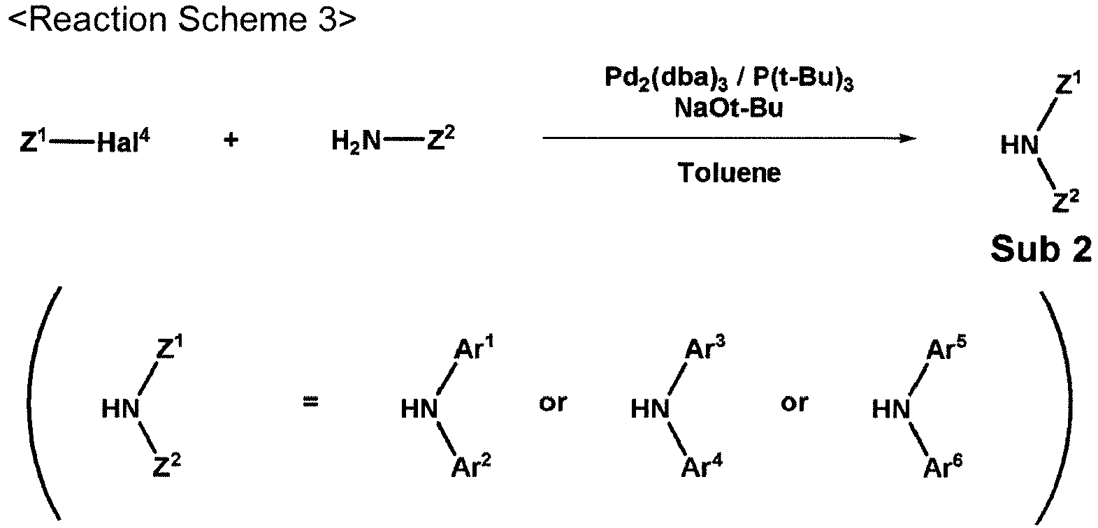
- Where Z1 is represented by Formula A-1 or Formula A-2, Z1-Hal4 of Reaction Scheme 3 may be synthesized by the reaction route of of the following Reaction Scheme 4, but there is no limitation thereto. X2, R3 to R6, o to r are the same as defined for Formula A-1 or Formula A-2, X' is -OH, -SH, -NH2, one of R4 and R6 is Hal4, and Hal5 is Br or Cl.


- The reaction proceeds according to the synthetic route of (1) where X' is -OH, the synthetic route of (2) where X' is -SH, and the synthetic route of (3) where X' is -NH2.
-

- After putting 2-iodobenzoic acid (50.0 g, 202 mmol), thiophenol (22.2 g, 202 mmol), Potassium hydroxide (56.6 g, 1008 mmol), Copper powder (1.3 g, 20.2 mmol) in a round bottom flask, water (1.3 L) was added thereto and the mixture was refluxed for 12 hours. When the reaction is completed, the reaction product was cooled to room temperature, and 3M HCI was added until precipitation was complete. Thereafter, the precipitate was washed with water and dried to obtain 41.3 g (yield 89%) of the product.
- After adding H2SO4 (1.3 mL) to the starting material Sub2-29-b (41.3 g, 179 mmol), the mixture was refluxed until the starting material was dissolved. When the starting material was dissolved, the solution was cooled to room temperature and then ice water was added to precipitate. After that, the precipitate was washed with water, dried and dissolved in CH2Cl2. Then, the resultant was separated through a silica gel column and recrystallized to obtain 25.9 g (yield 68%) of the product.
- 2-bromo-4'-chloro-1,1'-biphenyl (32.6 g, 122 mmol) was dissolved in THF (270 mL) under a nitrogen atmosphere, and then cooled to -78 °C. Then n-BuLi (49 mL) was slowly added thereto and the mixture was stirred for 30 minutes. Subsequently, after Sub2-29-c (25.9 g, 122 mmol) was dissolved in THF (140 mL), the solution was slowly added dropwise to the mixture. After stirring at -78°C for one hour, the temperature was gradually raised to room temperature. When the reaction is completed, the resultant was extracted with ethyl acetate and water, and the organic layer is dried with MgSO4 and concentrated. Thereafter, the concentrate was separated by a silica gel column and recrystallized to obtain 40.1 g (yield 82%) of the product.
- Sub2-29-d (40.1 g, 100 mmol), acetic acid (250 mL) and concentrated hydrochloric acid (40 mL) were placed in a round bottom flask and stirred under nitrogen atmosphere at 60-80°C for 3 hours. When the reaction was completed, the reaction product was extracted with CH2Cl2 and water, and the organic layer is dried with MgSO4 and concentrated. Thereafter, the concentrate was separated by a silica gel column and recrystallized to obtain 31.8 g (yield 83%) of the product.
- After dissolving Sub2-29-e (31.8 g, 83.0 mmol) in toluene (420 mL), aniline (7.7 g, 83.0 mmol), Pd2(dba)3 (2.28 g, 2.49 mmol), P(t-Bu)3 (1.01 g, 4.98 mmol) and NaOt-Bu (16.0 g, 166 mmol)) were added and stirred at 90°C. When the reaction was completed, the reaction product was extracted with CH2Cl2 and water, and the organic layer is dried with MgSO4 and concentrated. Thereafter, the concentrate was separated by a silica gel column and recrystallized to obtain 28.5 g (yield 78%) of the product.
-

- The reaction was carried out in the same manner as in the synthesis method of Sub2-29-b using 3-chloro-2-iodobenzoic acid (20.0 g, 70.8 mmol), 3-(dibenzo[b,d]furan-3-yl)benzenethiol (19.6 g, 70.8 mmol), KOH (19.9 g, 354 mmol), Copper powder (0.45 g, 7.08 mmol) to obtain 25.6 g (yield 84%).
- The reaction was carried out in the same manner as in the synthesis method of Sub2-29-c using Sub2-39-b (25.6 g, 59.4 mmol), H2SO4 (420 mL) to obtain 14.7 g (yield 60%).
- The reaction was carried out in the same manner as in the synthesis method of Sub2-29-d using 2-bromo-1,1'-biphenyl (8.3 g, 35.6 mmol), n-BuLi (14 mL), Sub2-39-c (14.7 g, 35.6 mmol) to obtain 16.4 g (yield 81%).
- The reaction was carried out in the same manner as in the synthesis method of Sub2-29-e using Sub2-39-d (16.4 g, 28.8 mmol), acetic acid (72 mL) and concentrated hydrochloric acid (12 mL) to obtain 12.0 g (yield 76%).
- The reaction was carried out in the same manner as in the synthesis method of Sub2-29 using Sub2-39-e (12.0 g, 21.9 mmol), aniline (2.0 g, 21.9 mmol), Pd2(dba)3 (0.60 g, 0.66 mmol), P(t-Bu)3 (0.27 g, 1.31 mmol), NaOt-Bu (4.2 g, 43.7 mmol) to obtain 9.4 g (yield 71%).
-

- After putting 2-iodobenzoic acid (50.0 g, 202 mmol), Phenol (37.9 g, 403 mmol), 1,8-diazabicyclo[5.4.0]undec-7-ene (DBU) (90.4 g, 605 mmol), pyridine (3.2 mL), copper powder (1.7 g, 26.2 mmol) and CuI (1.7 g, 9.07 mmol) in a round flask, DMF (1.6 L) was added thereto and the mixture was refluxed for 3 hours. When the reaction was completed, the reaction product was cooled to room temperature, and 3M HCI was added until precipitation was complete. Thereafter, the precipitate was washed with water and dried to obtain 41.8 g (yield 86%) of the product.
- The reaction was carried out in the same manner as in the synthesis method of Sub2-29-c using Sub2-46-b (41.8 g, 195 mmol), H2SO4 (14 L) to obtain 26.4 g (yield 69%) of product.
- The reaction was carried out in the same manner as in the synthesis method of Sub2-29-d using 2-bromo-2'-chloro-1,1'-biphenyl (36.0 g, 135 mmol), n-BuLi (54 mL), Sub2-46-c (26.4 g, 135 mmol) to obtain 45.1 g (yield 87%) of product.
- The reaction was carried out in the same manner as in the synthesis method of Sub2-29-e using Sub2-46-d (45.1 g, 117 mmol), acetic acid (290 mL) and concentrated hydrochloric acid (50 mL) to obtain 40.4 g (yield 94%) of product.
- The reaction was carried out in the same manner as in the synthesis method of Sub2-29 using Sub2-46-e (40.4 g, 110 mmol), aniline (10.3 g, 110 mmol), Pd2(dba)3 (3.03 g, 3.30 mmol), P(t-Bu)3 (1.34 g, 6.61 mmol), NaOt-Bu (21.2 g, 220 mmol) to obtain 35.0 g (yield 75%) of product.
-

- The reaction was carried out in the same manner as in the synthesis method of Sub2-46-b using 5-chloro-2-iodobenzoic acid (50.0 g, 177 mmol), Phenol (33.3 g, 354 mmol), 1,8-diazabicyclo[5.4.0]undec-7-ene (DBU) (79.4 g, 531 mmol), pyridine (2.9 mL), copper powder (1.5 g, 23.0 mmol), CuI (1.5 g, 7.97 mmol) to obtain 38.3 g (yield 87%) of product.
- The reaction was carried out in the same manner as in the synthesis method of Sub2-29-c using Sub2-47-b (38.3 g, 154 mmol), H2SO4 (1.1 L) to obtain 23.1 g (yield 65%) of product.
- The reaction was carried out in the same manner as in the synthesis method of Sub2-29-d using 2-bromo-1,1'-biphenyl (23.3 g, 100 mmol), n-BuLi (40 mL), Sub2-47-c (23.1 g, 100 mmol) to obtain 32.8 g (yield 85%) of product.
- The reaction was carried out in the same manner as in the synthesis method of Sub2-29-e using Sub2-47-d (32.8 g, 85.1 mmol), acetic acid (210 mL) and concentrated hydrochloric acid (35 mL) to obtain 28.4 g (yield 91%) of product.
- The reaction was carried out in the same manner as in the synthesis method of Sub2-29 using Sub2-47-e (28.4 g, 77.4 mmol), aniline (7.2 g, 77.4 mmol), Pd2(dba)3 (2.13 g, 2.32 mmol), P(t-Bu)3 (0.94 g, 4.65 mmol), NaOt-Bu (14.9 g, 155 mmol) to obtain 23.9 g (yield 73%) of product.
-
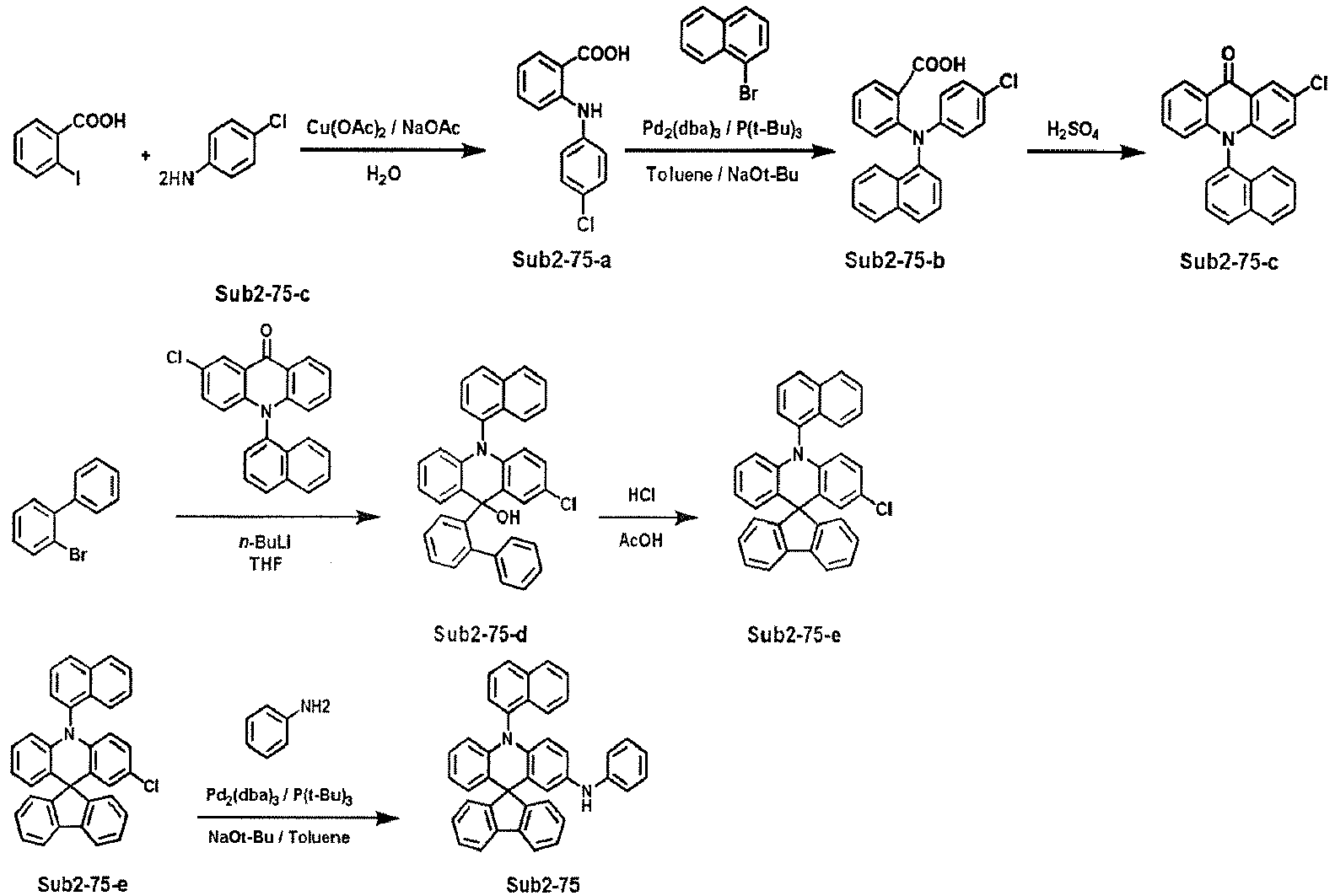
- After putting 2-iodobenzoic acid (20.0 g, 80.6 mmol), 4-chloroaniline (20.6 g, 161 mmol), Cu(OAc)2 (1.0 g), Sodium acetate (7.9 g, 96.8 mmol) in a round flask, water (540 mL) was added thereto and the mixture was refluxed for 5 hours. When the reaction was completed, the reaction product was cooled to room temperature, and 3M HCI was added until precipitation was complete. Thereafter, the precipitate was washed with water and dried to obtain 16.4 g (yield 82%) of the product.
- After dissolving Sub2-75-a (16.4 g, 66.2 mmol) in toluene (330 mL), 1-bromonaphthalene (13.7 g, 66.2 mmol), Pd2(dba)3 (1.82 g, 1.99 mmol), P(t-Bu)3 (0.80 g, 3.97 mmol) and NaOt-Bu (12.7 g, 132 mmol) were added the solution and the mixture was stirred at 60°C. When the reaction was completed, the reaction product was extracted with CH2Cl2 and water, and the organic layer was dried with MgSO4 and concentrated. Thereafter, the concentrate was separated by a silica gel column and recrystallized to obtain 18.3 g (yield 74%) of the product.
- The reaction was carried out in the same manner as in the synthesis method of Sub2-29-c using Sub2-75-b (18.3 g, 49.0 mmol), H2SO4 (350 mL) to obtain 11.8 g (yield 68%) of product.
- The reaction was carried out in the same manner as in the synthesis method of Sub2-29-d using 2-bromo-2'-chloro-1,1'-biphenyl (7.7 g, 33.2 mmol), n-BuLi (13 mL), Sub2-75-c (11.8 g, 33.2 mmol) to obtain 13.9 g (yield 82%) of product.
- The reaction was carried out in the same manner as in the synthesis method of Sub2-29-e using Sub2-75-d (13.9 g, 27.2 mmol), acetic acid (68 mL) and concentrated hydrochloric acid (11 mL) to obtain 12.3 g (yield 92%) of product.
- The reaction was carried out in the same manner as in the synthesis method of Sub2-29 using Sub2-75-e (12.3 g, 25.0 mmol), aniline (2.3 g, 25.0 mmol), Pd2(dba)3 (0.69 g, 0.75 mmol), P(t-Bu)3 (0.30 g, 1.50 mmol), NaOt-Bu (4.8 g, 50.0 mmol) to obtain 10.7 g (yield 78%) of product.
-

- 2-bromo-N-(4-chlorophenyl)-N-phenylnaphthalen-1-amine (20.0 g, 48.9 mmol) was dissolved in THF (100 mL) under a nitrogen atmosphere, and then cooled to -78 °C. Then n-BuLi (20 mL) was slowly added thereto and the mixture was stirred for 30 minutes. Subsequently, after 9H-fluoren-9-one (8.8 g, 48.9 mmol) was dissolved in THF (60 mL), the solution was slowly added dropwise to the mixture. After stirring at -78°C for one hour, the temperature was gradually raised to room temperature. When the reaction is completed, the resultant was extracted with ethyl acetate and water, and the organic layer is dried with MgSO4 and concentrated. Thereafter, the concentrate was separated by a silica gel column and recrystallized to obtain 21.2 g (yield 85%) of the product.
- The reaction was carried out in the same manner as in the synthesis method of Sub2-29-e using Sub2-81-f (21.2 g, 41.6 mmol), acetic acid (100 mL) and concentrated hydrochloric acid (20 mL) to obtain 9.8 g (yield 48%) of product.
- The reaction was carried out in the same manner as in the synthesis method of Sub2-29 using Sub2-81-e (9.8 g, 19.9 mmol), [1,1'-biphenyl]-4-amine (3.4 g, 19.9 mmol), Pd2(dba)3 (0.55 g, 0.60 mmol), P(t-Bu)3 (0.24 g, 1.20 mmol), NaOt-Bu (3.8 g, 39.8 mmol) to obtain 9.5 g (yield 76%) of product.
-

- The reaction was carried out in the same manner as in the synthesis method of Sub2-81-fusing 9-(2-bromo-4-chlorophenyl)-9H-carbazole (20.0 g, 56.1 mmol), n-BuLi (22 mL), 9H-fluoren-9-one (10.1 g, 56.1 mmol) to obtain 22.3 g (yield 81%) of product.
- The reaction was carried out in the same manner as in the synthesis method of Sub2-29-e using Sub2-83-f (22.3 g, 45.4 mmol), acetic acid (110 mL) and concentrated hydrochloric acid (20 mL) to obtain 17.8 g (yield 89%) of product.
- The reaction was carried out in the same manner as in the synthesis method of Sub2-29 using Sub2-83-e (17.8 g, 40.5 mmol), anilline (3.8 g, 40.5 mmol), Pd2(dba)3 (1.11 g, 1.21 mmol), P(t-Bu)3 (0.49 g, 2.43 mmol), NaOt-Bu (7.8 g, 80.9 mmol) to obtain 14.3 g (yield 71%) of product.
- The compounds belonging to Sub 2 may be, but not limited to, the following compounds, and Table 2 shows FD-MS(Field Desorption-Mass Spectrometry) values of the following compounds.





[Table 2] Compound FD-MS Compound FD-MS Sub 2-1 m/z=169.09(C12H11N=169.23) Sub 2-2 m/z=245.12(C18H15N=245.33) Sub 2-3 m/z=245.12(C18H15N=245.33) Sub 2-4 m/z=321.15(C24H19N=321.42) Sub 2-5 m/z=321.15(C24H19N=321.42) Sub 2-6 m/z=321.15(C24H19N=321.42) Sub 2-7 m/z=219.10(C16H13N=219.29) Sub 2-8 m/z=219.10(C16H13N=219.29) Sub 2-9 m/z=269.12(C20H15N=269.35) Sub 2-10 m/z=269.12(C20H15N= =269.35) Sub 2-11 m/z=421.18(C32H23N=421.54) Sub 2-12 m/z=421.18(C32H23N=421.54) Sub 2-13 m/z=179.15(C12HD10N=179.29) Sub 2-14 m/z=281.21 (C20H27N=281.44) Sub 2-15 m/z=281.21(C20H27N=281.44) Sub 2-16 m/z=241.15(C16H19NO=241.33) Sub 2-17 m/z=313.20(C20H27NO2=313.44) Sub 2-18 m/z=194.08(C13H10N2=194.24) Sub 2-19 m/z=187.08(C12H10FN=187.22) Sub 2-20 m/z=205.07(C12H9F2N=205.21) Sub 2-21 m/z=285.15(C21H19N=285.39) Sub 2-22 m/z=407.17(C31H21N=407.52) Sub 2-23 m/z=275.08(C18H13NS=275.37) Sub 2-24 m/z=259.10(C18H13NO=259.31) Sub 2-25 m/z=259.10(C18H13NO=259.31) Sub 2-26 m/z=325.09(C22H15NS=325.43) Sub 2-27 m/z=309.12(C22H15NO=309.37) Sub 2-28 m/z=309.12(C22H15NO=309.37) Sub 2-29 m/z=439.14(C31H21NS=439.58) Sub 2-30 m/z=439.14(C31H21NS=439.58) Sub 2-31 m/z=439.14(C31H21NS=439.58) Sub 2-32 m/z=439.14(C31H21NS=439.58) Sub 2-33 m/z=439.14(C31H21NS=439.58) Sub 2-34 m/z=439.14(C31H21NS=439.58) Sub 2-35 m/z=515.17(C37H25NS=515-67) Sub 2-36 m/z=489.16(C35H23NS=489.64) Sub 2-37 m/z=515.17(C37H25NS=515.67) Sub 2-38 m/z=515.17(C37H25NS=515.67) Sub 2-39 m/z=605.18(C43H27NOS=605.76) Sub 2-40 m/z=489.16(C35H23NS=489.64) Sub 2-41 m/z=489.16(C35H23NS=489.64) Sub 2-42 m/z=489.16(C35H23NS=489.64) Sub 2-43 m/z=489.16(C35H23NS=489.64) Sub 2-44 m/z=423.16(C31H21NO=423.52) Sub 2-45 m/z=423.16(C31H21NO=423.52) Sub 2-46 m/z=423.16(C31H21NO=423.52) Sub 2-47 m/z=423.16(C31H21NO=423.52) Sub 2-48 m/z=423.16(C31H21NO=42352) Sub 2-49 m/z=423.16(C31H21NO=423.52) Sub 2-50 m/z=423.16(C31H21NO=423.52) Sub 2-51 m/z=441.15(C31H20FNO=441.51) Sub 2-52 m/z=499.19(C37H25NO=499.61 Sub 2-53 m/z=499.19(C37H25NO=499.61) Sub 2-54 m/z=473.18(C35H23NO=473.58) Sub 2-55 m/z=473.18(C35H23NO=473.58) Sub 2-56 m/z=529.15(C37H23NOS=529.66) Sub 2-57 m/z=473.18(C35H23NO=473.58) Sub 2-58 m/z=473.18(C35H23NO=473.58) Sub 2-59 m/z=473.18(C35H23NO=473.58) Sub 2-60 m/z;473.18(C35H23NO=473.58) Sub 2-61 m/z=473.18(C35H23NO=473.58) Sub 2-62 m/z=473.18(C35H23)NO=473.58) Sub 2-63 m/z=473.18(C35H23NO=473.58) Sub 2-64 m/z=473.18(C35H23NO=473.58) Sub 2-65 m/z=498.21(C37H26N2=498.63) Sub 2-66 m/z=498.21(C37H26N2=498.63) Sub 2-67 m/z=498.21(C37H26N2=498.63) Sub 2-68 m/z=498.21 (C37H26N2=498.63) Sub 2-69 m/z=498.21(C37H26N2=498.63) Sub 2-70 m/z=498.21(C37H26N2=498.63) Sub 2-71 m/z=574.24(C43H30N2=574.73) Sub 2-72 m/z=574.24(C43H30N2=574.73) Sub 2-73 m/z=574.24(C43H30N2=574.73) Sub 2-74 m/z=548.23(C41H28N2=548.69) Sub 2-75 m/z=548.23(C41H28N2=548.69) Sub 2-76 m/z=548.23(C41H28N2=548.69) Sub 2-77 m/z=598.24(C45H30N2 =598.75) Sub 2-78 m/z=604.20(C43H28N2S=604.77) Sub 2-79 m/z=663.27(C49H33N3=663.82) Sub 2-80 m/z=614.27(C46H34N2=614.79) Sub 2-81 m/z=624.26(C47H32N2=624.79) Sub 2-82 m/z=496.19(C37H24N2=496.61) Sub 2-83 m/z=496.19(C37H24N2=496.61) Sub 2-84 m/z=496.19(C37H24N2=496.61) Sub 2-85 m/z=546.21(C41H26N2=546.67) Sub 2-86 m/z=528.17(C37H24N2S=528.67) Sub 2-87 m/z=528.17(C37H24N2S=528.67) Sub 2-88 m/z=528.17(C37H24N2S=528.67) Sub 2-89 m/z=512.19(C37H24N2O=512.61) Sub 2-90 m/z= 587.24(C43H29N3= 587.73) Sub 2-91 m/z=538.24(C40H30N2=538.69) -

- After dissolving Sub1-1 (2.00 g, 6.72 mmol) in toluene (35 mL), Sub2-1 (1.14 g, 6.72 mmol), Pd2(dba)3 (0.18 g, 0.20 mmol), P(t-Bu)3 (0.08 g, 0.40 mmol) and NaOt-Bu (1.29 g, 13.4 mmol) were added and stirred at 60°C. When the reaction was completed, the reaction product was extracted with CH2Cl2 and water, and the organic layer is dried with MgSO4 and concentrated. Thereafter, the concentrate was separated by a silica gel column and recrystallized to obtain 1.95 g (yield 75%) of the product.
- After Inter-1 (1.95 g, 5.04 mmol) was dissolved in toluene (25 mL), Sub2-29 (2.22 g, 5.04 mmol), Pd2(dba)3 (0.14 g, 0.15 mmol), P(t-Bu)3 (0.06 g, 0.30 mmol) and NaOt-Bu (0.97 g, 10.1 mmol) were added thereto and the mixture was refluxed. When the reaction was completed, the reaction product was extracted with CH2Cl2 and water, and the organic layer is dried with MgSO4 and concentrated. Thereafter, the concentrate was separated by a silica gel column and recrystallized to obtain 2.86 g (yield 72%) of the product.
-
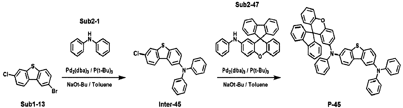
- The reaction was carried out in the same manner as in the synthesis method of Inter-1 using Sub1-13 (2.00 g, 6.72 mmol), Sub2-1 (1.14 g, 6.72 mmol), Pd2(dba)3 (0.18 g, 0.20 mmol), P(t-Bu)3 (0.08 g, 0.40 mmol), NaOt-Bu (1.29 g, 13.4 mmol) to obtain 1.87 g (yield 72%) of product.
- The reaction was carried out in the same manner as in the synthesis method of P-1 using Inter-45 (1.87 g, 4.84 mmol), Sub2-29 (2.05 g, 4.84 mmol), Pd2(dba)3 (0.13 g, 0.15 mmol), P(t-Bu)3 (0.06 g, 0.29 mmol), NaOt-Bu (0.93 g, 9.68 mmol) to obtain 2.62 g (yield 70%) of product.
-

- The reaction was carried out in the same manner as in the synthesis method of Inter-1 using Sub1-15 (2.00 g, 6.72 mmol), Sub2-1 (1.14 g, 6.72 mmol), Pd2(dba)3 (0.18 g, 0.20 mmol), P(t-Bu)3 (0.08 g, 0.40 mmol), NaOt-Bu (1.29 g, 13.4 mmol) to obtain 1.82 g (yield 70%) of product.
- The reaction was carried out in the same manner as in the synthesis method of P-1 using Inter-50 (1.82 g, 4.70 mmol), Sub2-44 (1.99 g, 4.70 mmol), Pd2(dba)3 (0.13 g, 0.14 mmol), P(t-Bu)3 (0.06 g, 0.28 mmol), NaOt-Bu (0.90 g, 9.41 mmol) to obtain 2.84 g (yield 78%) of product.
-

- The reaction was carried out in the same manner as in the synthesis method of Inter-1 using Sub1-16 (2.00 g, 6.72 mmol), Sub2-1 (1.14 g, 6.72 mmol), Pd2(dba)3 (0.18 g, 0.20 mmol), P(t-Bu)3 (0.08 g, 0.40 mmol), NaOt-Bu (1.29 g, 13.4 mmol) to obtain 2.00 g (yield 77%) of product.
- The reaction was carried out in the same manner as in the synthesis method of P-1 using Inter-64 (2.00 g, 5.17 mmol), Sub2-83 (2.57 g, 5.17 mmol), Pd2(dba)3 (0.14 g, 0.16 mmol), P(t-Bu)3 (0.06 g, 0.31 mmol), NaOt-Bu (0.99 g, 10.4 mmol) to obtain 3.15 g (yield 72%) of product.
-

- The reaction was carried out in the same manner as in the synthesis method of Inter-1 using Sub1-23 (2.00 g, 6.68 mmol), Sub2-4 (2.15 g, 6.68 mmol), Pd2(dba)3 (0.18 g, 0.20 mmol), P(t-Bu)3 (0.08 g, 0.40 mmol), NaOt-Bu (1.28 g, 13.4 mmol) to obtain 2.63 g (yield 73%) of product.
- The reaction was carried out in the same manner as in the synthesis method of P-1 using Inter-83 (2.63 g, 4.87 mmol), Sub2-75 (2.67 g, 4.87 mmol), Pd2(dba)3 (0.13 g, 0.15 mmol), P(t-Bu)3 (0.06 g, 0.29 mmol), NaOt-Bu (0.94 g, 9.75 mmol) to obtain 3.49 g (yield 68%) of product.
-

- After Sub1-32 (2.00 g, 7.10 mmol) was dissolved in toluene (40 mL), Sub2-45 (6.02 g, 14.21 mmol), Pd2(dba)3 (0.20 g, 0.21 mmol), P(t-Bu)3 (0.09 g, 0.43 mmol) and NaOt-Bu (1.37 g, 14.2 mmol) were added thereto and the mixture was refluxed. When the reaction was completed, the reaction product was extracted with CH2Cl2 and water, and the organic layer is dried with MgSO4 and concentrated. Thereafter, the concentrate was separated by a silica gel column and recrystallized to obtain 5.53 g (yield 77%) of the product.
-

- The reaction was carried out in the same manner as in the synthesis method of Inter-1 using Sub1-35 (2.00 g, 7.10 mmol), Sub2-1 (1.20 g, 7.10 mmol), Pd2(dba)3 (0.20 g, 0.21 mmol), P(t-Bu)3 (0.09 g, 0.43 mmol), NaOt-Bu (1.37 g, 14.2 mmol) to obtain 2.00 g (yield 76%) of product.
- The reaction was carried out in the same manner as in the synthesis method of P-1 using Inter-117 (2.00 g, 5.40 mmol), Sub2-29 (2.37 g, 5.40 mmol), Pd2(dba)3 (0.15 g, 0.16 mmol), P(t-Bu)3 (0.07 g, 0.32 mmol), NaOt-Bu (1.04 g, 10.8 mmol) to obtain 3.09 g (yield 74%) of product.
-

- The reaction was carried out in the same manner as in the synthesis method of Inter-1 using Sub1-37 (2.00 g, 7.10 mmol), Sub2-42 (3.36 g, 7.10 mmol), Pd2(dba)3 (0.20 g, 0.21 mmol), P(t-Bu)3 (0.09 g, 0.43 mmol), NaOt-Bu (1.37 g, 14.2 mmol) to obtain 3.40 g (yield 71%) of product.
- The reaction was carried out in the same manner as in the synthesis method of P-1 using Inter-132 (3.40 g, 5.04 mmol), Sub2-1 (0.85 g, 5.04 mmol), Pd2(dba)3 (0.14 g, 0.15 mmol), P(t-Bu)3 (0.06 g, 0.30 mmol), NaOt-Bu (0.97 g, 10.1 mmol) to obtain 3.22 g (yield 79%) of product.
-

- The reaction was carried out in the same manner as in the synthesis method of Inter-1 using Sub1-39 (2.00 g, 7.10 mmol), Sub2-87 (3.76 g, 7.10 mmol), Pd2(dba)3 (0.20 g, 0.21 mmol), P(t-Bu)3 (0.09 g, 0.43 mmol), NaOt-Bu (1.37 g, 14.2 mmol) to obtain 3.89 g (yield 75%) of product.
- The reaction was carried out in the same manner as in the synthesis method of P-1 using Inter-136 (3.89 g, 5.33 mmol), Sub2-13 (0.96 g, 5.33 mmol), Pd2(dba)3 (0.15 g, 0.16 mmol), P(t-Bu)3 (0.06 g, 0.32 mmol), NaOt-Bu (1.02 g, 10.7 mmol) to obtain 3.62 g (yield 78%) of product.
-

- The reaction was carried out in the same manner as in the synthesis method of Inter-1 using Sub1-40 (2.00 g, 7.10 mmol), Sub2-33 (3.12 g, 7.10 mmol), Pd2(dba)3 (0.20 g, 0.21 mmol), P(t-Bu)3 (0.09 g, 0.43 mmol), NaOt-Bu (1.37 g, 14.2 mmol) to obtain 3.55 g (yield 78%) of product.
- The reaction was carried out in the same manner as in the synthesis method of P-1 using Inter-145 (3.55 g, 5.54 mmol), Sub2-1 (0.94 g, 5.54 mmol), Pd2(dba)3 (0.15 g, 0.17 mmol), P(t-Bu)3 (0.07 g, 0.33 mmol), NaOt-Bu (1.07 g, 11.1 mmol) to obtain 2.87 g (yield 67%) of product.
-

- The reaction was carried out in the same manner as in the synthesis method of Inter-1 using Sub1-52 (2.00 g, 5.75 mmol), Sub2-1 (0.97 g, 5.75 mmol), Pd2(dba)3 (0.16 g, 0.17 mmol), P(t-Bu)3 (0.07 g, 0.35 mmol), NaOt-Bu (1.11 g, 11.5 mmol) to obtain 1.83 g (yield 73%) of product.
- The reaction was carried out in the same manner as in the synthesis method of P-1 using Inter-162 (1.83 g, 4.20 mmol), Sub2-45 (1.78 g, 4.20 mmol), Pd2(dba)3 (0.12 g, 0.13 mmol), P(t-Bu)3 (0.05 g, 0.25 mmol), NaOt-Bu (0.81 g, 8.40 mmol) to obtain 2.63 g (yield 76%) of product.
-

- The reaction was carried out in the same manner as in the synthesis method of Inter-1 using Sub1-65 (2.00 g, 5.24 mmol), Sub2-1 (0.89 g, 5.24 mmol), Pd2(dba)3 (0.14 g, 0.16 mmol), P(t-Bu)3 (0.06 g, 0.31 mmol), NaOt-Bu (1.01 g, 10.5 mmol) to obtain 1.77 g (yield 72%) of product.
- The reaction was carried out in the same manner as in the synthesis method of P-1 using Inter-175 (1.77 g, 3.77 mmol), Sub2-83 (1.87 g, 3.77 mmol), Pd2(dba)s (0.10 g, 0.11 mmol), P(t-Bu)3 (0.05 g, 0.23 mmol), NaOt-Bu (0.73 g, 7.55 mmol) to obtain 2.49 g (yield 71%) of product.
-

- The reaction was carried out in the same manner as in the synthesis method of Inter-1 using Sub1-85 (2.00 g, 5.59 mmol), Sub2-44 (2.37 g, 5.59 mmol), Pd2(dba)3 (0.15 g, 0.17 mmol), P(t-Bu)3 (0.07 g, 0.34 mmol), NaOt-Bu (1.07 g, 11.2 mmol) to obtain 3.17 g (yield 81%) of product.
- The reaction was carried out in the same manner as in the synthesis method of P-1 using Inter-195 (3.17 g, 4.53 mmol), Sub2-1 (0.77 g, 4.53 mmol), Pd2(dba)3 (0.12 g, 0.14 mmol), P(t-Bu)3 (0.05 g, 0.27 mmol), NaOt-Bu (0.87 g, 9.06 mmol) to obtain 2.45 g (yield 65%) of product.
-

- The reaction was carried out in the same manner as in the synthesis method of Inter-1 using Sub1-90 (2.00 g, 7.16 mmol), Sub2-5 (2.30 g, 7.16 mmol), Pd2(dba)3 (0.20 g, 0.21 mmol), P(t-Bu)3 (0.09 g, 0.43 mmol), NaOt-Bu (1.38 g, 14.3 mmol) to obtain 3.05 g (yield 82%) of product.
- After adding an excess of trifluoromethane-sulfonic acid to Inter-204-a (3.05 g, 5.87 mmol), the solution was stirred for 24 hours at room temperature. Water and pyridine (8:1) were slowly added the solution and the mixture was refluxed for 30 minutes. After lowering the temperature, the resultant was extracted with CH2Cl2 and water. The organic layer was dried withr MgSO4 and concentrated. Thereafter, the concentrate was separated by a silica gel column and recrystallized to obtain 1.89 g (yield: 73%) of the product.
- The reaction was carried out in the same manner as in the synthesis method of P-1 using Inter-204-b (1.89 g, 4.29 mmol), Sub2-33 (2.80 g, 4.29 mmol), Pd2(dba)3 (0.12 g, 0.13 mmol), P(t-Bu)3 (0.05 g, 0.26 mmol), NaOt-Bu (0.82 g, 8.58 mmol) to obtain 2.91 g (yield 72%) of product.
-

- The reaction was carried out in the same manner as in the synthesis method of Inter-1 using Sub1-92 (2.00 g, 6.72 mmol), Sub2-1 (1.14 g, 6.72 mmol), Pd2(dba)3 (0.18 g, 0.20 mmol), P(t-Bu)3 (0.08 g, 0.40 mmol), NaOt-Bu (1.29 g, 13.4 mmol) to obtain 1.84 g (yield 71%) of product.
- The reaction was carried out in the same manner as in the synthesis method of P-1 using Inter-208 (1.84 g, 4.77 mmol), Sub2-32 (2.10 g, 4.77 mmol), Pd2(dba)3 (0.13 g, 0.14 mmol), P(t-Bu)3 (0.06 g, 0.29 mmol), NaOt-Bu (0.92 g, 9.54 mmol) to obtain 3.09 g (yield 82%) of product.
-

- The reaction was carried out in the same manner as in the synthesis method of Inter-1 using Sub1-96 (2.00 g, 6.72 mmol), Sub2-47 (2.85 g, 6.72 mmol), Pd2(dba)3 (0.18 g, 0.20 mmol), P(t-Bu)3 (0.08 g, 0.40 mmol), NaOt-Bu (1.29 g, 13.4 mmol) to obtain 3.36 g (yield 78%) of product.
- The reaction was carried out in the same manner as in the synthesis method of P-1 using Inter-216 (3.36 g, 5.24 mmol), Sub2-1 (0.89 g, 5.24 mmol), Pd2(dba)3 (0.14 g, 0.16 mmol), P(t-Bu)3 (0.06 g, 0.31 mmol), NaOt-Bu (1.01 g, 10.5 mmol) to obtain 3.08 g (yield 76%) of product.
-

- The reaction was carried out in the same manner as in the synthesis method of Inter-1 using Sub1-106 (2.00 g, 7.10 mmol), Sub2-1 (1.20 g, 7.10 mmol), Pd2(dba)3 (0.20 g, 0.21 mmol), P(t-Bu)3 (0.09 g, 0.43 mmol), NaOt-Bu (1.37 g, 14.2 mmol) to obtain 1.92 g (yield 73%) of product.
- The reaction was carried out in the same manner as in the synthesis method of P-1 using Inter-243 (1.92 g, 5.19 mmol), Sub2-34 (2.28 g, 5.19 mmol), Pd2(dba)3 (0.14 g, 0.16 mmol), P(t-Bu)3 (0.06 g, 0.31 mmol), NaOt-Bu (1.00 g, 10.4 mmol) to obtain 1.72 g (yield 43%) of product.
-

- The reaction was carried out in the same manner as in the synthesis method of Inter-1 using Sub1-102 (2.00 g, 7.10 mmol), Sub2-1 (1.20 g, 7.10 mmol), Pd2(dba)3 (0.20 g, 0.21 mmol), P(t-Bu)3 (0.09 g, 0.43 mmol), NaOt-Bu (1.37 g, 14.2 mmol) to obtain 2.02 g (yield 77%) of product.
- After dissolving Inter-250-a (2.02 g, 5.47 mmol) in THF (27 mL), (4-hydroxyphenyl) boronic acid (0.75 g, 5.47 mmol), NaOH (0.66 g, 16.4 mmol), Pd(PPh3)4 (0.38 g, 0.33 mmol) and water (14 mL) were added and the mixture was stirred at 80°C. When the reaction was completed, the reaction product was extracted with CH2Cl2 and water, and the organic layer is dried with MgSO4 and concentrated. Thereafter, the concentrate was separated by a silica gel column and recrystallized to obtain 1.92 g (yield: 82%) of the product.
- The reaction was carried out in the same manner as in the synthesis method of Inter-204-b using Inter-250-b (1.92 g, 4.49 mmol) to obtain 1.83 g (yield: 73%) of product.
- The reaction was carried out in the same manner as in the synthesis method of P-1 using Inter-250-c (1.83 g, 3.27 mmol), Sub2-47 (1.39 g, 3.27 mmol), Pd2(dba)3 (0.09 g, 0.10 mmol), P(t-Bu)3 (0.04 g, 0.20 mmol), NaOt-Bu (0.63 g, 6.55 mmol) to obtain 2.05 g (yield 75%) of product.
-
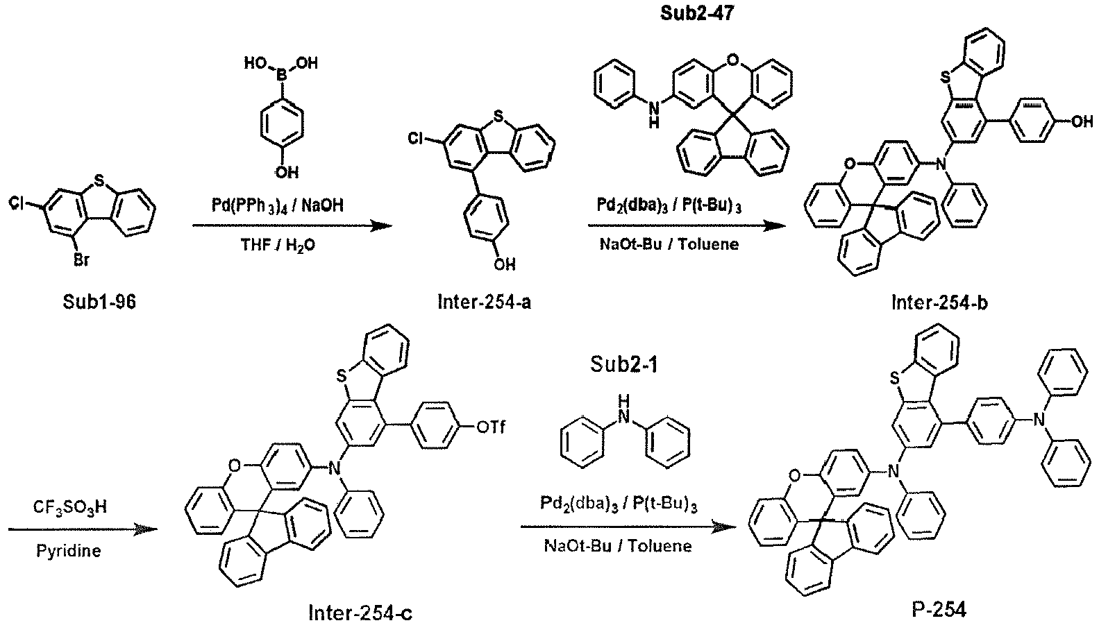
- The reaction was carried out in the same manner as in the synthesis method of Inter-250-b using Sub1-96 (2.0 g, 6.72 mmol), (4-hydroxyphenyl) boronic acid (0.93 g, 6.72 mmol), NaOH (0.81 g, 20.2 mmol), Pd(PPh3)4 (0.47 g, 0.40 mmol) to obtain 1.75 g (yield: 84%) of product.
- The reaction was carried out in the same manner as in the synthesis method of Inter-1 using Inter-254-a (1.75 g, 5.65 mmol), Sub2-47 (2.39 g, 5.65 mmol), Pd2(dba)3 (0.16 g, 0.17 mmol), P(t-Bu)3 (0.07 g, 0.34 mmol), NaOt-Bu (1.09 g, 11.3 mmol) to obtain 2.84 g (yield 72%) of product.
- The reaction was carried out in the same manner as in the synthesis method of Inter-204-b using Inter-254-b (2.84 g, 4.06 mmol) to obtain 2.56 g (yield: 76%) of product.
- The reaction was carried out in the same manner as in the synthesis method of P-1 using Inter-254-c (2.56 g, 3.09 mmol), Sub2-1 (0.52 g, 3.09 mmol), Pd2(dba)3 (0.08 g, 0.09 mmol), P(t-Bu)3 (0.04 g, 0.19 mmol), NaOt-Bu (0.59 g, 6.18 mmol) to obtain 1.89 g (yield 72%) of product.
- The FD-MS values of the compounds P-1 to P-266 of the present invention prepared according to the above synthesis examples are shown in Table 3 below.
[Table 3] Compound FD-MS Compound FD-MS P-1 m/z=788.23(C55H36N2S2=789.03) P-2 m/z=848.29(C61H40N2OS=849.06) P-3 m/z=860.29(C59H44N2OS2=861.13) P-4 m/z=897.32(C65H43N3S=898.14) P-5 m/z=822.27(C59H38N2OS=823.03) P-6 m/z=923.33(C67H45N3S=924.18) P-7 m/z=845.29(C61H39N3S=846.06) P-8 m/z=838.25(C59H38N2S2=839.09) P-9 m/z=877.26(C61H39N3S2=878.12) P-10 m/z=1119.33(C79H49N3OS2=1120.4) P-11 m/z=782.32(C55H26D10N2OS=783.03) P-12 m/z=963.36(C70H49N3S=964.24) P-13 m/z=836.29(C60H40N2OS=837.05) P-14 m/z=990.26(C67H40F2N2OS2=991.19) P-15 m/z=879.27(C61H38FN3OS=880.05) P-16 m/z=998.34(C72H46N4S=999.25) P-17 m/z=1016.33(C73H48N2S2=1017.32) P-18 m/z=782.32(C55H26D10N2OS=783.03) P-19 m/z=974.33(C71H46N2OS=975.22) P-20 m/z=1012.36(C73H48N4S=1013.28) P-21 m/z=864.26(C61H40N2S2=865.13) P-22 m/z=973.35(C71H47N3S=974.24) P-23 m/z=886.30(C64H42N2OS=887.11) P-24 m/z=916.37(C63H52N2O3S=917.18) P-25 m/z=957.41(C69H55N3S=958.28) P-26 m/z=894.22(C61H38N2S3=895.17) P-27 m/z=1115.43(C82H57N3S=1116.44) P-28 m/z=872.29(C63H40N2OS=873.09) P-29 m/z=788.23(C55H36N2S2=789.03) P-30 m/z=942.31(C67H43FN2OS=943.15) P-31 m/z=847.30(C61H41N3S=848.08) P-32 m/z=1053.38(C76H51N3OS=1054.32) P-33 m/z=940.29(C67H44N2S2=941.22) P-34 m/z=786.27(C56H38N2OS=786.99) P-35 m/z=847.30(C61H41N3S=848.08) P-36 m/z=838.25(C59H38N2S2=839.09) P-37 m/z=940.29(C67H44N2S2=941.22) P-38 m/z=822.27(C59H38N2OS=823.03) P-39 m/z=847.30(C61H41N3S=848.08) P-40 m/z=786.27(C56H36N2OS=786.99) P-41 m/z=772.25(C55H36N2OS=772.97) P-42 m/z=788.23(C55H36N2S2=789.03) P-43 m/z=861.32(C62H43N3S=862.11) P-44 m/z=772.25(C55H36N2OS=772.97) P-45 m/z=772.25(C55H36N2OS=772.97) P-46 m/z=788.23(C55H36N2S2=789.03) P-47 m/z=847.30(C61H41N3S=848.08) P-48 m/z=802.25(C56H38N2S2=803.05) P-49 m/z=788.23(C55H36N2S2=789.03) P-50 m/z=772.25(C55H36N2OS=772.97) P-51 m/z=847.30(C61H41N3S=848.08) P-52 m/z=788.23(C55H36N2S2=789.03) P-53 m/z=940.29(C67H44N2S2=941.22) P-54 m/z=822.27(C59H36N2OS=823.03) P-55 m/z=897.32(C65H43N3S=898.14) P-56 m/z=772.25(C55H36N2OS=772.97) P-57 m/z=824.21 (C55H34F2N2S2=825.01) P-58 m/z=924.32(C67H44N2OS=925.16) P-59 m/z=959.43(C69H57N3S=960.30) P-60 m/z=877.26(C61H39N3S2=878.12) P-61 m/z=888.26(C63H40N2S2=889.15) P-62 m/z=947.33(C69H45N3S=948.20) P-63 m/z=772.25(C55H36N2OS=772.97) P-64 m/z=845.29(C61H39N3S=846.06) P-65 m/z=772.25(C55H36N2OS=772.97) P-66 m/z=904.29(C64H44N2S2=905.19) P-67 m/z=1099.40(C81H53N3S=1100.40) P-68 m/z=772.25(C55H36N2OS=772.97) P-69 m/z=928.26(C65H40N2OS2=929.17) P-70 m/z=772.25(C55H36N2OS=772.97) P-71 m/z=947.33(C69H45N3S=948.20) P-72 m/z=788.23(C55H36N2S2=789.03) P-73 m/z=788.23(C55H36N2S2=789.03) P-74 m/z=772.25(C55H36N2OS=772.97) P-75 m/z=1003.31(C71H45N3S2=1004.28) P-76 m/z=900.36(C63H52N2S2=901.24) P-77 m/z=848.29(C61H40N2OS=849.06) P-78 m/z=920.35(C67H44N4O=921.12) P-79 m/z=848.29(C61H40N2OS=849.06) P-80 m/z=921.30(C66H39N3O3=922.06) P-81 m/z=786.29(C56H38N2O3=786.93) P-82 m/z=772.25(C55H36N2OS=772.97) P-83 m/z=1051.39(C77H50FN3O=1052.27) P-84 m/z=931.36(C69H45N3O=932.14) P-85 m/z=806.29(C59H38N2O2=806.97) P-86 m/z=782.32(C55H26D10N2OS=783.03) P-87 m/z=931.36(C69H45N3O=932.14) P-88 m/z=862.27(C61H38N2O2S=863.05) P-89 m/z=924.32(C67H44N2OS=925.16) P-90 m/z=824.28(C59H37FN2O2=824.96) P-91 m/z=908.34(C67H44N2O2=909.10) P-92 m/z=845.34(C62H43N3O=846.05) P-93 m/z=848.29(C61H40N2OS=849.06) P-94 m/z=861.34(C62H43N3O2=862.05) P-95 m/z=797.25(C56H35N3OS=797.98) P-96 m/z=774.27(C55H35FN2O2=774.90) P-97 m/z=924.32(C67H44N2OS=925.16) P-98 m/z=879.32(C65H41N3O=880.06) P-99 m/z=832.31(C61H40N2O2=833.00) P-100 m/z=848.29(C61H40N2OS=849.06) P-101 m/z=808.24(C55H34F2N2OS=808.95) P-102 m/z=766.34(C55H26D10N2O2=766.97) P-103 m/z=1083.42(C81H53N3O=1084.34) P-104 m/z=797.25(C56H35N3OS=797.98) P-105 m/z=856.31(C63H40N2O2=857.03) P-106 m/z=772.25(C55H36N2OS=772.97) P-107 m/z=983.39(C73H49N3O=984.22) P-108 m/z=1010.33(C74H46N2OS=1011.26) P-109 m/z=884.38(C63H52N2OS=885.18) P-110 m/z=925.35(C67H44FN3O=926.11) P-111 m/z=856.31(C63H40N2O2=857.03) P-112 m/z=1010.35(C74H46N2O3=1011.19) P-113 m/z=867.31(C61H39F2N3O=868.00) P-114 m/z=781.27(C56H35N3O2=781.92) P-115 m/z=1126.36(C82H50N2O2S=1127.37) P-116 m/z=912.28(C65H40N2O2S=913.11) P-117 m/z=772.25(C55H36N2OS=772.97) P-118 m/z=907.36(C67H43N3O=908.12) P-119 m/z=756.28(C55H36N2O2=756.91) P-120 m/z=786.27(C56H38N2OS=786.99) P-121 m/z=756.28(C55H36N2O2=756.91) P-122 m/z=786.27(C56H38N2OS=786.99) P-123 m/z=943.34(C67H43F2N3O=944.10) P-124 m/z=772.25(C55H36N2OS=772.97) P-125 m/z=772.25(C55H36N2OS=772.97) P-126 m/z=822.27(C59H38N2OS=823.03) P-127 m/z=983.39(C73H49N3O=984.22) P-128 m/z=806.29(C59H38N2O2=806.97) P-129 m/z=790.25(C55H35FN2OS=790.96) P-130 m/z=908.34(C67H44N2O2=909.10) P-131 m/z=931.36(C69H45N3O=932.14) P-132 m/z=806.29(C59H38N2O2=806.97) P-133 m/z=806.29(C59H38N2O2=806.97) P-134 m/z=884.38(C63H52N2OS=885.18) P-135 m/z=831.32(C61H41N3O=832.02) P-136 m/z=871.34(C61H29D10N3OS=872.12) P-137 m/z=808.24(C55H34F2N2OS=808.95) P-138 m/z=808.24(C55H34F2N2OS=808.95) P-139 m/z=957.37(C71H47N3O=958.18) P-140 m/z=832.31(C61H40N2O2=833.00) P-141 m/z=772.25(C55H36N2OS=772.97) P-142 m/z=806.29(C59H38N2O2=806.97) P-143 m/z=867.31(C61H39F2N3O=868.00) P-144 m/z=981.37(C73H47N3O=982.20) P-145 m/z=848.29(C61H40N2OS=849.06) P-146 m/z=756.28(C55H36N2O2=756.91) P-147 m/z=1000.35(C73H48N2OS=1001.26) P-148 m/z=831.32(C61H41N3O=832.02) P-149 m/z=756.28(C55H36N2O2=756.91) P-150 m/z=756.28(C55H36N2O2=756.91) P-151 m/z=831.32(C61H41N3O=832.02) P-152 m/z=772.25(C55H36N2OS=772.97) P-153 m/z=838.25(C59H38N2S2=839.09) P-154 m/z=806.29(C59H38N2O2=806.97) P-155 m/z=822.27(C59H38N2OS=823.03) P-156 m/z=897.32(C65H43N3S=898.14) P-157 m/z=822.27(C59H38N2OS=823.03) P-158 m/z=838.25(C59H38N2S2=839.09) P-159 m/z=987.33(C71H45N3OS=988.22) P-160 m/z=822.27(C59H38N2OS=823.03) P-161 m/z=838.25(C59H38N2S2=839.09) P-162 m/z=822.27(C59H38N2OS=823.03) P-163 m/z=822.27(C59H38N2OS=823.03) P-164 m/z=881.34(C65H43N3O=882.08) P-165 m/z=888.26(C63H40N2S2=889.15) P-166 m/z=947.33(C69H45N3S=948.20) P-167 m/z=856.31(C63H40N2O2=857.03) P-168 m/z=872.29(C63H40N2OS=873.09) P-169 m/z=872.29(C63H40N2OS=873.09) P-170 m/z=947.33(C69H45N3S=948.20) P-171 m/z=872.29(C63H40N2OS=873.09) P-172 m/z=872.29(C63H40N2OS=873.09) P-173 m/z=872.29(C63H40N2OS=873.09) P-174 m/z=872.29(C63H40N2OS=873.09) P-175 m/z=929.34(C69H43N3O=930.12) P-176 m/z=872.29(C63H40N2OS=873.09) P-177 m/z=888.26(C63H40N2S2=889.15) P-178 m/z=872.29(C63H40N2OS=873.09) P-179 m/z=931.36(C69H45N3O=932.14) P-180 m/z=872.29(C63H40N2OS=873.09) P-181 m/z=872.29(C63H40N2OS=873.09) P-182 m/z=977.29(C69H43N3S2=978.24) P-183 m/z=931.36(C59H45N3O=932.14) P-184 m/z=856.31(C63H40N2O2=857.03) P-185 m/z=872.29(C63H40N2OS=873.09) P-186 m/z=947.33(C69H45N3S=948.20) P-187 m/z=656.31(C63H40N2O2=857.03) P-188 m/z=872.29(C63H40N2OS=873.09) P-189 m/z=848.29(C61H40N2OS=849.06) P-190 m/z=898.30(C65H42N2OS=899.12) P-191 m/z=907.36(C67H45N3O=908.12) P-192 m/z=848.29(C61H40N2OS=849.06) P-193 m/z=914.28(C65H42N2S2=915.19) P-194 m/z=1029.32(C73H47N3S2=1030.32) P-195 m/z=832.31 (C61 H40N2O2=833.00) P-196 m/z=864.32(C62H44N2OS=865.11) P-197 m/z=898.3(C65H42N2OS=899.12) P-198 m/z=914.28(C65H42N2S2=915.19) P-199 m/z=788.23(C55H36N2S2=789.03) P-200 m/z=847.30(C61 H41 N3S=848.08) P-201 m/z=772.25(C55H36N2OS=772.97) P-202 m/z=954.27(C67H42N2OS2=955.21) P-203 m/z=887.32(C61H29D10N3S2=888.19) P-204 m/z=940.29(C67H44N2S2=941.22) P-205 m/z=838.23(C56H36F2N2S2=839.03) P-206 m/z=924.32(C67H44N2OS=925.16) P-207 m/z=999.36(C73H49N3S=1000.28) P-208 m/z=788.23(C55H36N2S2=789.03) P-209 m/z=864.26(C61H40N2S2=865.13) P-210 m/z=847.30(C61H41N3S=848.08) P-211 m/z=772.25(C55H36N2OS=772.97) P-212 m/z=887.33(C64H45N3S=888.15) P-213 m/z=888.32(C64H44N2OS=889.13) P-214 m/z=972.33(C70H44N4S=973.21) P-215 m/z=924.32(C67H44N2OS=925.16) P-216 m/z=772.25(C55H36N2OS=772.97) P-217 m/z=865.29(C61H40FN3S=866.07) P-218 m/z=772.25(C55H36N2OS=772.97) P-219 m/z=844.29(C59H44N2S2=845.14) P-220 m/z=845.29(C61H39N3S=846.06) P-221 m/z=848.29(C61H40N2OS=849.06) P-222 m/z=786.29(C56H38N2O3=786.93) P-223 m/z=831.32(C61H41N3O=832.02) P-224 m/z=772.25(C55H36N2OS=772.97) P-225 m/z=886.28(C62H36N4OS=887.07) P-226 m/z=756.28(C55H36N2O2=756.91) P-227 m/z=983.39(C73H49N3O=984.22) P-228 m/z=884.38(C63H52N2OS=885.18) P-229 m/z=772.25(C55H36N2OS=772.97) P-230 m/z=983.39(C73H49N3O=984.22) P-231 m/z=908.34(C67H44N2O2=909.10) P-232 m/z=772.25(C55H36N2OS=772.97) P-233 m/z=831.32(C61H41N3O=832.02) P-234 m/z=826.23(C55H33F3N2OS=826.94) P-235 m/z=756.28(C65H36N2O2=756.91) P-236 m/z=772.25(C55H36N2OS=772.97) P-237 m/z=844.31 (C59H44N2O2S=845.07) P-238 m/z=849.32(C61 H40FN3O=850.01) P-239 m/z=908.34(C67H44N2O2=909.10) P-240 m/z=829.31(C61H39N3O=830.00) P-241 m/z=772.25(C55H36N2OS=772.97) P-242 m/z=756.28(C55H36N2O2=756.91) P-243 m/z=772.25(C55H36N2OS=772.97) P-244 m/z=881.34(C65H43N3O=882.08) P-245 m/z=848.29(C61 H40N2OS=849.06) P-246 m/z=923.33(C67H45N3S=924.18) P-247 m/z=848.29(C61H40N2OS=849.06) P-248 m/z=832.31(C61H40N2O2=833.00) P-249 m/z=864.26(C61H40N2S2=865.13) P-250 m/z=832.31(C61H40N2O2=833.00) P-251 m/z=907.36(C67H45N3O=908.12) P-252 m/z=864.26(C61H40N2S2=865.13) P-253 m/z=923.33(C67H45N3S=924.18) P-254 m/z=848.29(C61 H40N2OS=849.06) P-255 m/z=907.36(C67H45N3O=908.12) P-256 m/z=848.29(C61H40N2OS=849.06) P-257 m/z=848.29(C61H40N2OS=849.06) P-258 m/z=848.29(C61H40N2OS=849.06) P-259 m/z=939.33(C67H45N3OS=940.18) P-260 m/z=939.33(C67H45N3OS=940.18) P-261 m/z=838.25(C59H38N2S2=839.09) P-262 m/z=806.29(C59H38N2O2=806.97) P-263 m/z=822.27(C59H38N2OS=823.03) P-264 m/z=822.27(C59H38N2OS=823.03) P-265 m/z=973.35(C71H47N3S=974.24) P-266 m/z=882.32(C65H42N2O2=883.06) - After vacuum-depositing 4,4',4"-Tris[2-naphthyl(phenyl)amino]triphenylamine (hereinafter, "2-TNATA") on an ITO layer (anode) formed on a glass substrate to form a hole injection layer with a thickness of 60 nm , a hole transport layer with a thickness of 60 nm was formed by vacuum-depositing N,N'-bis(1-naphthalenyl)-N,N'-bis-phenyl-(1,1'-biphenyl)-4,4'-diamine (hereinafter, "NPB") on the hole injection layer.
- Subsequently, an emission-auxiliary layer with a thickness of 20 nm was formed by vacuum-depositing the compound P-1 of the present invention on the hole transport layer and 4,4'-N,N'-dicarbazole-biphenyl(hereinafter, "CBP") as a host material and bis-(1-phenylisoquinolyl)iridium(III)acetylacetonate (hereinafter, "(piq)2Ir(acac)") as a dopant material in a weight ratio of 95:5 were deposited on the emission-auxiliary layer to form a light emitting layer with a thickness of 30 nm.
- Subsequently, (1,1'-bisphenyl-4-olato)bis(2-methyl-8-quinolinolato)aluminum (hereinafter, " BAlq") was vacuum-deposited to a thickness of 10 nm on the light emitting layer to form a hole blocking layer, and tris-(8-hydroxyquinoline)aluminum(hereinafter, "Alq3") was vacuum-deposited to a thickness of 40 nm on the hole blocking layer to form a an electron transport layer.
- Thereafter, LiF was deposited to a thickness of 0.2 nm to form an electron injection layer, and then Al was deposited to a thickness of 150 nm to form a cathode.
- The organic electroluminescent elements were fabricated in the same manner as described in Example 1 except that the compounds of the present invention described in the following Table 4, instead of compound P-1 of the present invention, were used as material of an emission-auxiliary layer.
- The organic electroluminescent element was fabricated in the same manner as in Example 1, except that an emission-auxiliary layer was not formed.
- The organic electroluminescent elements were fabricated in the same manner as described in Example 1 except that Comparative Compound A or B were used as material of an emission-auxiliary layer.

- Electroluminescence (EL) characteristics were measured with PR-650 (Photoresearch) by applying a forward bias DC voltage to the organic electroluminescent elements prepared in Examples 1 to 44 of the present invention and Comparative Examples 1 to 3. And, the T95 life time was measured using a life time measuring apparatus manufactured by ms science Inc. at reference brightness of 2500 cd/m2. The measurement results are shown in Tables 4 below.
[Table 4] Compound Voltage (V) Current Density (mA/cm2) Brightness (cd/m2) Efficiency (cd/A) Lifetime T(95) CIE x y comp.Ex(1) - 6.7 34.2 2500 7.3 62.9 0.61 0.31 comp.Ex(2) comp.Com A 5.8 14.5 2500 17.2 85.0 0.60 0.34 comp.Ex(3) comp.Com B 5.0 10.4 2500 24.0 113.2 0.61 0.30 Ex.(1) Com.(P-1) 4.8 10.1 2500 24.8 151.4 0.62 0.33 Ex.(2) Com.(P-2) 4.8 9.7 2500 25.8 163.0 0.62 0.33 Ex.(3) Com.(P-4) 4.8 10.6 2500 23.5 131.6 0.63 0.33 Ex.(4) Com.(P-9) 5.1 10.5 2500 23.7 131.8 0.63 0.31 Ex.(5) Com.(P-21) 4.9 10.3 2500 24.2 148.6 0.61 0.33 Ex.(6) Com.(P-31) 5.1 10.6 2500 23.6 131.7 0.61 0.35 Ex.(7) Com.(P-33) 4.8 10.2 2500 24.5 149.9 0.64 0.34 Ex.(8) Com.(P-41) 4.8 8.9 2500 28.0 177.7 0.64 0.32 Ex.(9) Com.(P-42) 4.8 9.5 2500 26.4 161.9 0.61 0.35 Ex.(10) Com.(P-44) 4.9 9.1 2500 27.4 174.4 0.60 0.32 Ex.(11) Com.(P-45) 4.8 9.2 2500 27.2 172.7 0.61 0.34 Ex.(12) Com.(P-50) 4.9 9.1 2500 27.5 174.4 0.65 0.34 Ex.(13) Com.(P-59) 4.9 10.8 2500 23.1 129.2 0.62 0.32 Ex.(14) Com.(P-64) 4.8 11.0 2500 22.8 127.9 0.63 0.31 Ex.(15) Com.(P-70) 4.9 9.6 2500 25.9 164.7 0.65 0.32 Ex.(16) Com.(P-83) 5.0 10.9 2500 22.9 134.3 0.63 0.33 Ex.(17) Com.(P-89) 5.3 10.7 2500 23.4 151.5 0.63 0.31 Ex.(18) Com.(P-106) 5.1 10.2 2500 24.4 157.6 0.62 0.34 Ex.(19) Com.(P-112) 5.1 9.7 2500 25.7 171.1 0.63 0.33 Ex.(20) Com.(P-117) 5.1 9.8 2500 25.4 149.2 0.61 0.34 Ex.(21) Com.(P-118) 5.2 10.0 2500 25.0 147.9 0.64 0.34 Ex.(22) Com.(P-131) 5.1 10.3 2500 24.3 142.4 0.61 0.31 Ex.(23) Com.(P-132) 5.2 9.9 2500 25.1 167.7 0.63 0.31 Ex.(24) Com.(P-138) 5.0 9.9 2500 25.3 167.9 0.60 0.32 Ex.(25) Com.(P-141) 5.1 9.7 2500 25.7 165.3 0.61 0.34 Ex.(26) Com.(P-145) 5.1 10.1 2500 24.7 159.1 0.61 0.30 Ex.(27) Com.(P-148) 5.2 10.6 2500 23.6 138.3 0.61 0.31 Ex.(28) Com.(P-162) 4.8 9.2 2500 27.1 172.5 0.63 0.34 Ex.(29) Com.(P-192) 5.0 9.9 2500 25.2 140.9 0.61 0.34 Ex.(30) Com.(P-195) 5.3 9.3 2500 27.0 181.4 0.61 0.30 Ex.(31) Com.(P-196) 5.0 10.2 2500 24.6 156.0 0.62 0.31 Ex.(32) Com.(P-204) 4.9 9.8 2500 25.6 148.8 0.61 0.31 Ex.(33) Com.(P-208) 4.9 10.0 2500 25.1 148.5 0.63 0.31 Ex.(34) Com.(P-211) 5.0 9.7 2500 25.9 164.5 0.62 0.33 Ex.(35) Com.(P-216) 4.9 9.0 2500 27.7 166.3 0.60 0.34 Ex.(36) Com.(P-220) 5.0 11.0 2500 22.8 127.8 0.61 0.34 Ex.(37) Com.(P-223) 5.2 10.9 2500 22.9 134.4 0.63 0.34 Ex.(38) Com.(P-226) 5.1 9.2 2500 27.3 171.1 0.63 0.33 Ex.(39) Com.(P-243) 5.2 10.6 2500 23.6 151.4 0.61 0.31 Ex.(40) Com.(P-248) 5.2 9.1 2500 27.5 173.0 0.65 0.31 Ex.(41) Com.(P-250) 5.3 9.5 2500 26.4 171.3 0.64 0.31 Ex.(42) Com.(P-251) 5.3 10.6 2500 23.5 138.3 0.63 0.32 Ex.(43) Com.(P-254) 5.0 8.9 2500 28.1 168.0 0.62 0.32 Ex.(44) Com.(P-262) 5.1 9.4 2500 26.6 167.8 0.61 0.34 - The results of Comparative Example 2 or Comparative Example 3 using Comparative Compound A or Comparative Compound B were superior to Comparative Example 1 not forming an emission-auxiliary layer, and it can be seen that Example 1 to Example 44 of the present invention are remarkably superior in lifetime.
- Table 5 below shows the physical property values of Compound P-45 of the present invention, Comparative Compound A, Comparative Compound B, and NPB.
[Table 5] Compound Compound P-45 comp.ComA comp.ComB NPB G.HOMO -4.84 -4.67 -4.87 -4.71 G.LUMO -1.00 -0.99 -1.14 -1.12 G.Band Gap 3.84 3.68 3.73 3.59 - Comparing compound of the present invention with Comparative Compound A, the linking group between the amino group and the amino group is carbazole in Comparative Compound A, while dibenzofuran and dibenzothiophene are introduced as the linking group in compound of the present invention.
- As can be seen in Table 5, where carbazole is introduced as a linker (Comparative Compound A), the HOMO value is higher than that of the compound of the present invention in which dibenzofuran or dibenzothiophene is introduced, and has a higher HOMO value than the NPB used as a material for the hole transport layer in Example 1.
- Therefore, in the case of Comparative Compound A, the hole is not easily moved to the host compared to compound of the present invention, and the hole is accumulated. As a result, the charge balance in the light emitting layer is decreased, so that the efficiency and lifetime are significantly lower than compound of the present invention.
- Comparing compound of the present invention with Comparative Compound B, Comparative compound B is a structure in which dibenzofuran is introduced as a substituent of an amino group, while spiro[fluorene-9,9'-xanthene], spiro[fluorene-9,9'-thioxanthene], spiro[acridine-9,9'-fluorene], etc. are introduced as substituents in compound of the present invention.
- As can be seen from Table 5, compound of the present invention has a higher LUMO value than Comparative Compound B in which dibenzofuran is substituted, so that electrons moving from the host to the hole transport layer can be more effectively blocked. Therefore, damage to the hole transport layer or an emission-auxiliary layer can be minimized, as a result, it appears that lifetime is significantly improved.
- In the case of an emission-auxiliary layer, even if a similar core is used, it will be very difficult for a person skilled in the art to infer the characteristics exibiting when the compound of the present invention is used in an emission-auxiliary layer becasuse the relationship between the hole transport layer and the light-emitting layer (host) needs to be understood.
- In addition, in the evaluation results of the above-mentioned element fabrication, even if the characteristics of element are described in the case where compound of the present invention is applied to an emission-auxiliary layer have been described, compound of the present invention can be applied to a hole transport layer or to both a hole transport layer and an emission-auxiliary layer.
- Although the exemplary embodiments of the present invention have been described for illustrative purposes, those skilled in the art to which the present invention pertains will be capable of various modifications without departing from the essential characteristics of the present invention. Therefore, the embodiment disclosed herein is intended to illustrate the scope of the technical idea of the present invention, and the spirit and scope of the present invention are not limited by the embodiments. The scope of the present invention shall be construed on the basis of the accompanying claims, and it shall be construed that all of the technical ideas included within the scope equivalent to the claims belong to the present invention.
Claims (14)
- A compound of Formula 1:

Ar1 to Ar6 are each independently selected from the group consisting of a C6-C60 aryl group, a fluorenyl group, a C2-C60 heterocyclic group containing at least one heteroatom of O, N, S, Si, and P, a C3-C60 aliphatic ring group, -L'-N(Ra)(Rb), Formula A-1 and Formula A-2, and at least one of Ar1 to Ar6 is Formula A-1 or Formula A-2, X1 is O or S,X2 is N(R'), O or S,R1 to R6 are each independently selected from the group consisting of hydrogen, deuterium, halogen, cyano group, nitro group, a C6-C60 aryl group, a fluorenyl group, a C2-C60 heterocyclic group containing at least one heteroatom of O, N, S, Si, and P, a C3-C60 aliphatic ring group, a C1-C30 alkyl group, a C2-C30 alkenyl group, a C2-C30 alkynyl group, a C1-C30 alkoxyl group, a C6-C30 aryloxy group and -L'-N(Ra)(Rb), and adjacent groups together may be bonded to each other to form a ring,n, p' and r' are each an integer of 0 to 3, m, o, p, q and r are each an integer of 0 to 4, where they are each an integer of 2 or more, each of R1s, each of R2s, each of R3s, each of R4s, each of R5s, each of R6s is the same or different from each other,x and y are each an integer of 0 to 2, and x+y is an integer greater than or equal to 1,L1 to L3 and L' are each independently selected from the group consisting of a single bond, a C6-C60 arylene group, a fluorenylene group, a C3-C60 aliphatic ring group and a C2-C60 heterocyclic group containing at least one heteroatom of O, N, S, Si, and P,R', Ra and Rb are each independently selected from the group consisting of a C6-C60 aryl group, a fluorenyl group, a C2-C60 heterocyclic group containing at least one heteroatom of O, N, S, Si, and P and a C3-C60 aliphatic ring group,Ar1 to Ar6, R1 to R6, L1 to L3, R' and the ring formed by adjacent groups may be each optionally substituted with one or more substituents selected from the group consisting of deuterium, halogen, a silane group unsubstituted or substituted with a C1-C20 alkyl group or a C6-C20 aryl group, a siloxane group, a boron group, a germanium group, a cyano group, a nitro group, a C1-C20 alkylthio group, a C1-C20 alkoxyl group, a C6-C20 aryloxy group, a C6-C20 arylthio group, a C1-C20 alkyl group, a C2-C20 alkenyl group, a C2-C20 alkynyl group, a C6-C20 aryl group, a fluorenyl group, a C2-C20 heterocyclic group containing at least one heteroatom of O, N, S, Si, and P, a C3-C20 aliphatic ring group, a C7-C20 arylalkyl group, and C8-C20 arylalkenyl group.
 - The compound of claim 1, wherein Formula 1 is represented by Formula 2 or Formula 3:


- The compound of claim 1, wherein Formula 1 is represented by one of Formula 4 to Formula 19:


- The compound of claim 1, wherein Formula 1 is represented by one of Formula 20 to Formula 34:


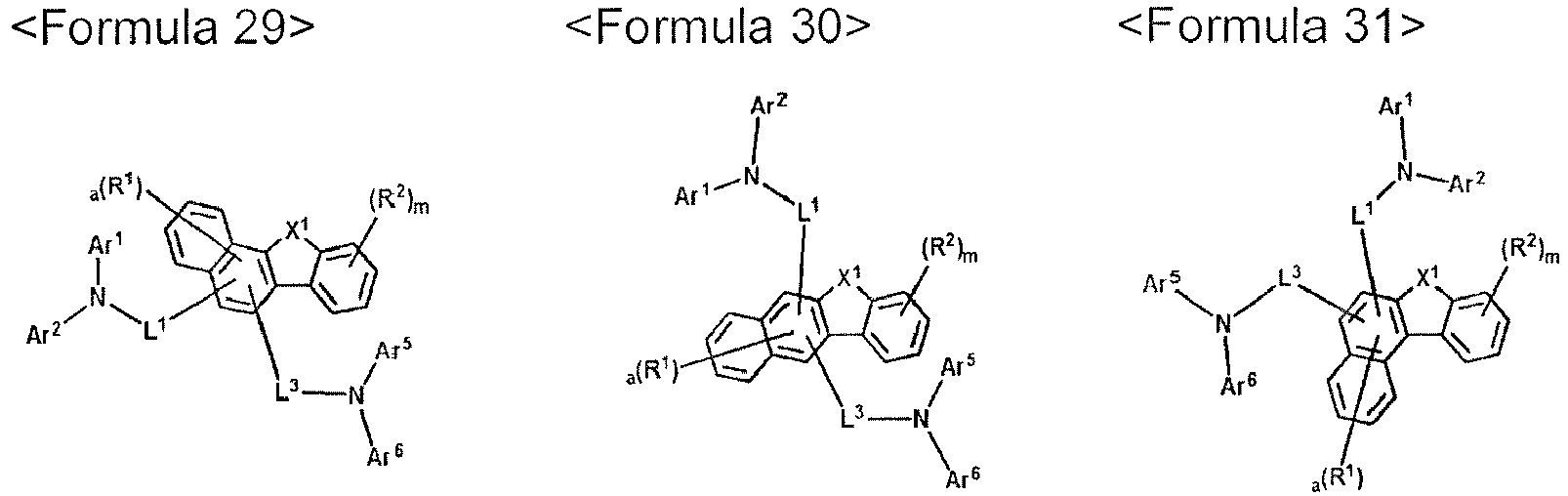

- The compound of claim 1, wherein at least one of L1 to L3 is a single bond.
- The compound of claim 1, wherein the compound represented by Formula 1 is one of the following compounds:


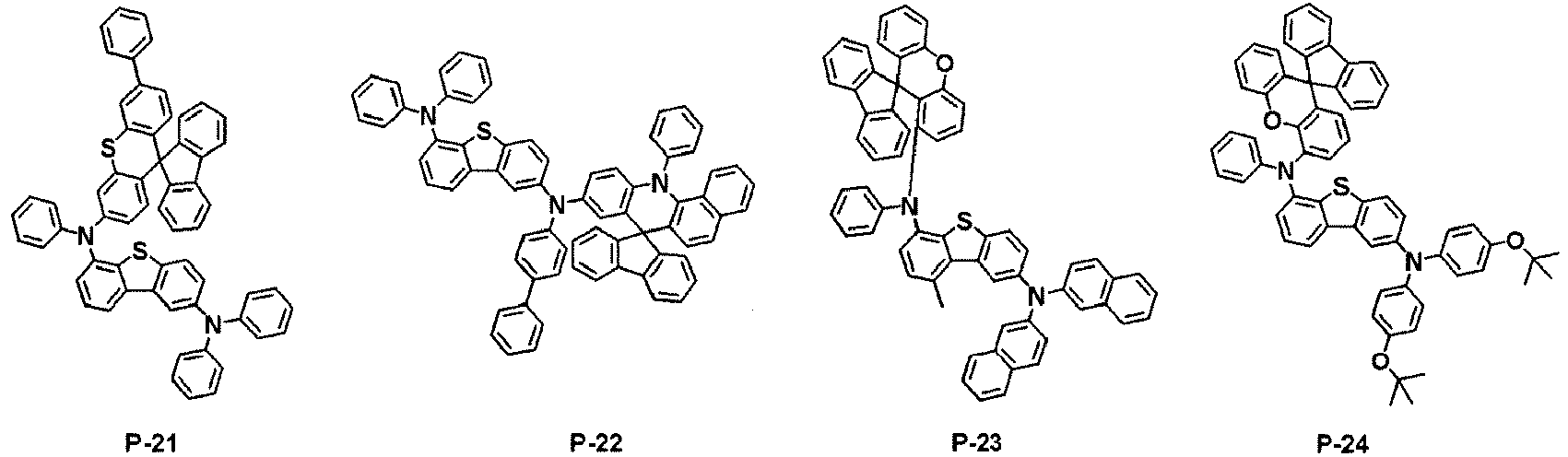


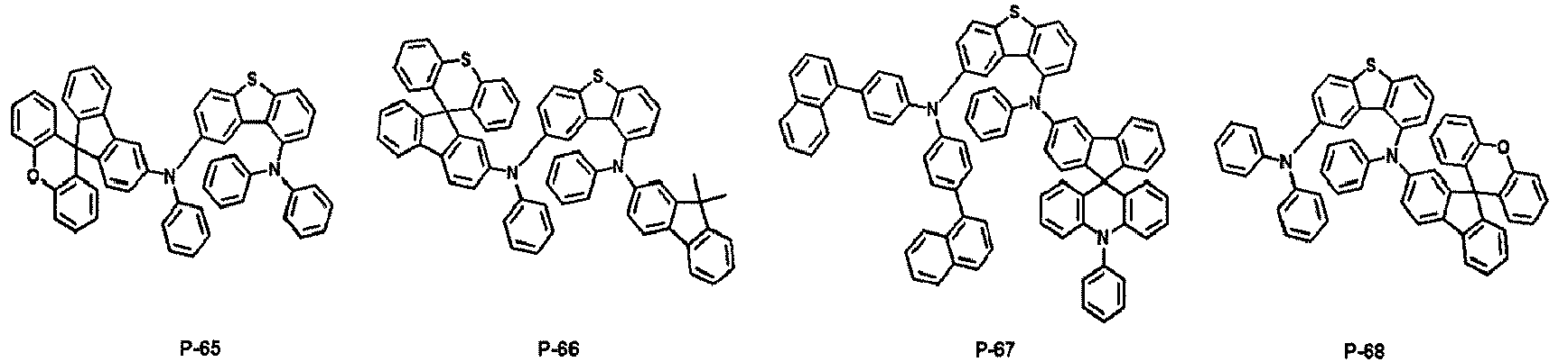


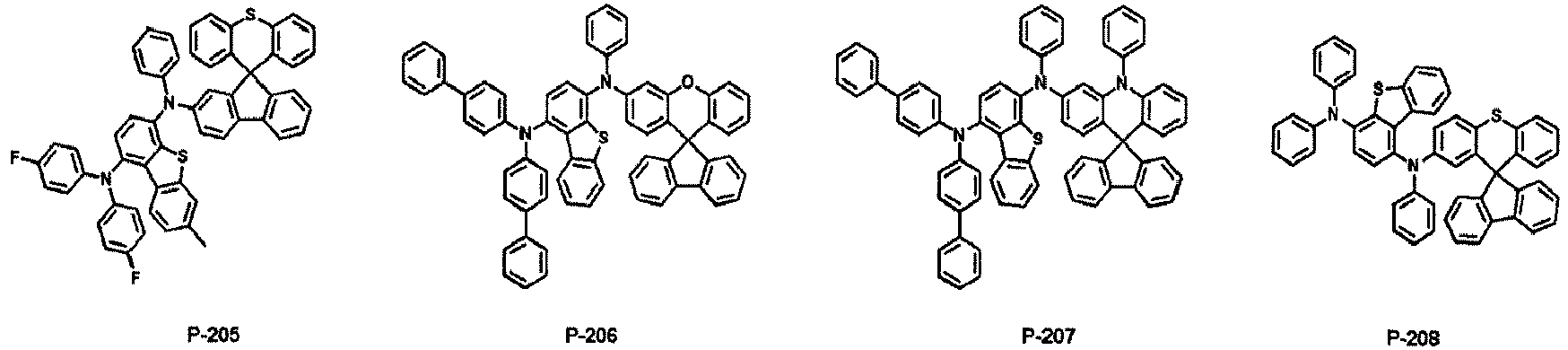


- An organic electric element comprising an anode, a cathode, and an organic material layer formed between the anode and the cathode, wherein the organic material layer comprises a single compound or two or more compounds represented by Formula 1 of any one of claims 1 to 6.
- An organic electric element comprising an anode, a cathode, an organic material layer formed between the anode and the cathode, and a layer for improving luminous efficiency, wherein the layer for improving luminous efficiency is formed on one side of the anode and/or the cathode, the one side is not facing the organic material layer, and the organic material layer or the layer for improving luminous efficiency comprises a single compound or two or more compounds represented by Formula 1 of any one of claims 1 to 6.
- The organic electric element of claim 7 or 8, wherein the organic material layer comprises at least one of a hole injection layer, a hole transport layer, an emission-auxiliary layer, a light emitting layer, an electron transport-auxiliary layer, an electron transport layer and an electron injection layer.
- The organic electric element of claim 9, wherein the compound is comprised in the emission-auxiliary layer.
- The organic electric element of claim 7 or 8, wherein the organic material layer comprises two or more stacks and the stacks comprise the hole transport layer, the light emitting layer and the electron transport layer formed sequentially on the anode.
- The organic electric element of claim 11, wherein the organic electric element further comprises the charge generation layer formed between the stacks.
- An electronic device comprising a display device and a control unit for driving the display device, wherein the display device comprises the organic electric element of claim 7 or 8.
- The electronic device of claim 13, wherein the organic electric element is selected from the group consisting of an organic electroluminescent element, an organic solar cell, an organic photo conductor, an organic transistor, an element for monochromatic illumination and an element for quantum dot display.
Applications Claiming Priority (3)
| Application Number | Priority Date | Filing Date | Title |
|---|---|---|---|
| KR20190083318 | 2019-07-10 | ||
| KR1020190101535A KR102820538B1 (en) | 2019-07-10 | 2019-08-20 | Compound for organic electronic element, organic electronic element using the same, and an electronic device thereof |
| KR1020200057682A KR102142095B1 (en) | 2019-07-10 | 2020-05-14 | Compound for organic electronic element, organic electronic element using the same, and an electronic device thereof |
Publications (2)
| Publication Number | Publication Date |
|---|---|
| EP3764416A1 true EP3764416A1 (en) | 2021-01-13 |
| EP3764416B1 EP3764416B1 (en) | 2022-01-26 |
Family
ID=72040121
Family Applications (1)
| Application Number | Title | Priority Date | Filing Date |
|---|---|---|---|
| EP20185207.6A Active EP3764416B1 (en) | 2019-07-10 | 2020-07-10 | Compound for organic electronic element, organic electronic element using the same, and an electronic device thereof |
Country Status (5)
| Country | Link |
|---|---|
| US (1) | US12552809B2 (en) |
| EP (1) | EP3764416B1 (en) |
| JP (1) | JP7078230B2 (en) |
| KR (2) | KR102820538B1 (en) |
| CN (1) | CN117777120A (en) |
Cited By (3)
| Publication number | Priority date | Publication date | Assignee | Title |
|---|---|---|---|---|
| EP4039683A4 (en) * | 2019-11-19 | 2022-11-30 | Duk San Neolux Co., Ltd. | Compound for organic electrical element, organic electrical element using same and electronic device thereof |
| US11925112B2 (en) | 2019-11-19 | 2024-03-05 | Duk San Neolux Co., Ltd. | Compound for organic electronic element, organic electronic element using the same, and an electronic device thereof |
| US12545667B2 (en) | 2019-11-19 | 2026-02-10 | Duk San Neolux Co., Ltd. | Compound for organic electronic element, organic electronic element using the same, and an electronic device thereof |
Families Citing this family (3)
| Publication number | Priority date | Publication date | Assignee | Title |
|---|---|---|---|---|
| WO2022108141A1 (en) * | 2020-11-18 | 2022-05-27 | 엘티소재주식회사 | Compound and organic light-emitting device comprising same |
| KR102820668B1 (en) * | 2020-12-14 | 2025-06-16 | 덕산네오룩스 주식회사 | Compound for organic electronic element, organic electronic element using the same, and an electronic device thereof |
| KR20220086271A (en) * | 2020-12-16 | 2022-06-23 | 주식회사 센텀머티리얼즈 | Novel heterocyclic compound and organic light emitting device comprising the same |
Citations (10)
| Publication number | Priority date | Publication date | Assignee | Title |
|---|---|---|---|---|
| KR101251451B1 (en) | 2012-08-17 | 2013-04-05 | 덕산하이메탈(주) | Compound for organic electronic element, organic electronic element using the same, and a electronic device thereof |
| WO2014072017A1 (en) * | 2012-11-12 | 2014-05-15 | Merck Patent Gmbh | Materials for electronic devices |
| US20170237013A1 (en) * | 2016-02-11 | 2017-08-17 | Duk San Neolux Co., Ltd. | Compound for organic electronic element, organic electronic element using the same, and an electronic device thereof |
| WO2018056649A1 (en) * | 2016-09-20 | 2018-03-29 | 덕산네오룩스 주식회사 | Compound for organic electronic element, organic electronic element using same and electronic device therefor |
| JP2018108939A (en) * | 2016-12-28 | 2018-07-12 | 出光興産株式会社 | Compound, material for organic electroluminescent element, organic electroluminescent element, and electronic apparatus |
| EP3385265A1 (en) * | 2015-12-01 | 2018-10-10 | Duk San Neolux Co., Ltd. | Compound for organic electric device, organic electric device using same, and electronic device |
| US20190088879A1 (en) * | 2017-08-03 | 2019-03-21 | Idemitsu Kosan Co., Ltd. | Compound, material for organic electroluminescence devices, organic electroluminescence device, and electronic device |
| EP3466926A1 (en) * | 2016-05-26 | 2019-04-10 | Duk San Neolux Co., Ltd. | Compound for organic electronic element, organic electronic element using same and electronic device therefor |
| CN109867652A (en) * | 2017-12-04 | 2019-06-11 | Cmdl有限公司 | Novel Organic Compounds and Organic Electroluminescent Devices Containing the Same |
| US20190189927A1 (en) * | 2016-07-29 | 2019-06-20 | Duk San Neolux Co., Ltd. | Compound for organic electronic element, organic electronic element using same, and electronic device thereof |
Family Cites Families (13)
| Publication number | Priority date | Publication date | Assignee | Title |
|---|---|---|---|---|
| US7015639B2 (en) | 2002-10-22 | 2006-03-21 | Osram Opto Semiconductors Gmbh | Electroluminescent devices and method of making transparent cathodes |
| KR100925323B1 (en) * | 2006-12-01 | 2009-11-04 | 주식회사 엘지화학 | Novel compound and organic light emitting device using same |
| US9178163B2 (en) | 2010-05-26 | 2015-11-03 | Duk San Neolux Co., Ltd. | Compound comprising a five-membered hetero ring, an organic electrical element using same and a terminal thereof |
| KR101351417B1 (en) | 2010-10-26 | 2014-01-14 | 엘지디스플레이 주식회사 | White organic light emitting device |
| KR102357590B1 (en) * | 2015-04-13 | 2022-02-03 | 덕산네오룩스 주식회사 | Compound for organic electric element, organic electric element comprising the same and electronic device thereof |
| KR102552251B1 (en) * | 2016-06-17 | 2023-07-06 | 덕산네오룩스 주식회사 | Compound for organic electronic element, organic electronic element comprising the same, and electronic device thereof |
| KR102758692B1 (en) * | 2016-10-05 | 2025-01-22 | 에스에프씨 주식회사 | Organic light-emitting diode with long lifetime, low voltage and high efficiency |
| KR102122213B1 (en) * | 2017-01-04 | 2020-06-12 | 에스에프씨주식회사 | organic light-emitting diode with High efficiency |
| CN106977491B (en) | 2017-01-25 | 2020-06-19 | 孙立成 | Spiro [ fluorene-9, 9-xanthene ] hole transport material and application thereof |
| JP6975959B2 (en) * | 2017-07-25 | 2021-12-01 | 国立大学法人山形大学 | Arylamine derivatives, hole transport materials using them, and organic EL devices |
| KR102611877B1 (en) * | 2017-12-21 | 2023-12-08 | 덕산네오룩스 주식회사 | Compound for organic electronic element, organic electronic element comprising the same, and electronic device thereof |
| EP3727370A4 (en) | 2017-12-22 | 2021-11-17 | Energy Everywhere, Inc. | Fused and cross-linkable ionic hole transport materials for perovskite solar cells |
| WO2020218680A1 (en) * | 2019-04-25 | 2020-10-29 | 두산솔루스 주식회사 | Organic compound and organic electroluminescent diode using same |
-
2019
- 2019-08-20 KR KR1020190101535A patent/KR102820538B1/en active Active
-
2020
- 2020-05-14 KR KR1020200057682A patent/KR102142095B1/en active Active
- 2020-07-10 EP EP20185207.6A patent/EP3764416B1/en active Active
- 2020-07-10 CN CN202311324377.8A patent/CN117777120A/en active Pending
- 2020-07-10 JP JP2020119432A patent/JP7078230B2/en active Active
-
2023
- 2023-10-02 US US18/479,306 patent/US12552809B2/en active Active
Patent Citations (10)
| Publication number | Priority date | Publication date | Assignee | Title |
|---|---|---|---|---|
| KR101251451B1 (en) | 2012-08-17 | 2013-04-05 | 덕산하이메탈(주) | Compound for organic electronic element, organic electronic element using the same, and a electronic device thereof |
| WO2014072017A1 (en) * | 2012-11-12 | 2014-05-15 | Merck Patent Gmbh | Materials for electronic devices |
| EP3385265A1 (en) * | 2015-12-01 | 2018-10-10 | Duk San Neolux Co., Ltd. | Compound for organic electric device, organic electric device using same, and electronic device |
| US20170237013A1 (en) * | 2016-02-11 | 2017-08-17 | Duk San Neolux Co., Ltd. | Compound for organic electronic element, organic electronic element using the same, and an electronic device thereof |
| EP3466926A1 (en) * | 2016-05-26 | 2019-04-10 | Duk San Neolux Co., Ltd. | Compound for organic electronic element, organic electronic element using same and electronic device therefor |
| US20190189927A1 (en) * | 2016-07-29 | 2019-06-20 | Duk San Neolux Co., Ltd. | Compound for organic electronic element, organic electronic element using same, and electronic device thereof |
| WO2018056649A1 (en) * | 2016-09-20 | 2018-03-29 | 덕산네오룩스 주식회사 | Compound for organic electronic element, organic electronic element using same and electronic device therefor |
| JP2018108939A (en) * | 2016-12-28 | 2018-07-12 | 出光興産株式会社 | Compound, material for organic electroluminescent element, organic electroluminescent element, and electronic apparatus |
| US20190088879A1 (en) * | 2017-08-03 | 2019-03-21 | Idemitsu Kosan Co., Ltd. | Compound, material for organic electroluminescence devices, organic electroluminescence device, and electronic device |
| CN109867652A (en) * | 2017-12-04 | 2019-06-11 | Cmdl有限公司 | Novel Organic Compounds and Organic Electroluminescent Devices Containing the Same |
Cited By (5)
| Publication number | Priority date | Publication date | Assignee | Title |
|---|---|---|---|---|
| EP4039683A4 (en) * | 2019-11-19 | 2022-11-30 | Duk San Neolux Co., Ltd. | Compound for organic electrical element, organic electrical element using same and electronic device thereof |
| EP4215528A1 (en) * | 2019-11-19 | 2023-07-26 | Duk San Neolux Co., Ltd. | Compound for organic electrical element, organic electrical element using same and electronic device thereof |
| US11925112B2 (en) | 2019-11-19 | 2024-03-05 | Duk San Neolux Co., Ltd. | Compound for organic electronic element, organic electronic element using the same, and an electronic device thereof |
| US12274163B2 (en) | 2019-11-19 | 2025-04-08 | Duk San Neolux Co., Ltd. | Compound for organic electrical element, organic electrical element using same and electronic device thereof |
| US12545667B2 (en) | 2019-11-19 | 2026-02-10 | Duk San Neolux Co., Ltd. | Compound for organic electronic element, organic electronic element using the same, and an electronic device thereof |
Also Published As
| Publication number | Publication date |
|---|---|
| US20240057476A1 (en) | 2024-02-15 |
| JP2021014455A (en) | 2021-02-12 |
| CN117777120A (en) | 2024-03-29 |
| KR20210007782A (en) | 2021-01-20 |
| EP3764416B1 (en) | 2022-01-26 |
| JP7078230B2 (en) | 2022-05-31 |
| KR102142095B1 (en) | 2020-08-06 |
| KR102820538B1 (en) | 2025-06-13 |
| US12552809B2 (en) | 2026-02-17 |
Similar Documents
| Publication | Publication Date | Title |
|---|---|---|
| EP3764416B1 (en) | Compound for organic electronic element, organic electronic element using the same, and an electronic device thereof | |
| US12193321B2 (en) | Compound for organic electric element, organic electric element comprising the same, and electronic device thereof | |
| EP3730490A1 (en) | Compound for organic electronic device, organic electronic device using same, and electronic device therefor | |
| KR102374470B1 (en) | Compound for organic electronic element, organic electronic element using the same, and an electronic device thereof | |
| EP3305766A1 (en) | Compound for organic electrical element, organic electrical element using same, and electronic device therefor | |
| KR102690463B1 (en) | Compound for organic electric element, organic electric element using the same, and an electronic device thereof | |
| KR20190135707A (en) | Compound for organic electronic element, organic electronic element using the same, and an electronic device thereof | |
| US20250057038A1 (en) | Compound for organic electric element, organic electric element using the same, and an electronic device thereof | |
| KR20210013452A (en) | Compound for organic electronic element, organic electronic element using the same, and an electronic device thereof | |
| EP4620944A1 (en) | Compound for organic electric element, organic electric element using same, and electronic device having same | |
| KR20230014596A (en) | Compound for organic electronic element, organic electronic element using the same, and an electronic device thereof | |
| KR20220077279A (en) | Compound for organic electronic element, organic electronic element using the same, and an electronic device thereof | |
| KR102736898B1 (en) | Compound for organic electronic element, organic electronic element using the same, and an electronic device thereof | |
| KR102407840B1 (en) | Compound for organic electronic element, organic electronic element using the same, and an electronic device thereof | |
| KR20210145002A (en) | Compound for organic electronic element, organic electronic element using the same, and an electronic device thereof | |
| US12295258B2 (en) | Compound for organic electronic element, organic electronic element using the same, and an electronic device thereof | |
| KR102768900B1 (en) | Compound for organic electronic element, organic electronic element using the same, and an electronic device thereof | |
| EP4592298A1 (en) | Compound for organic electrical element, organic electrical element using same, and electronic device thereof | |
| KR102402086B1 (en) | Compound for organic electronic element, organic electronic element using the same, and an electronic device thereof | |
| KR20210152606A (en) | Compound for organic electronic element, organic electronic element using the same, and an electronic device thereof | |
| KR20240037559A (en) | Compound for organic electronic element, organic electronic element using the same, and an electronic device thereof | |
| KR20240005586A (en) | Compound for organic electric element, organic electric element using the same, and an electronic device thereof | |
| US20240376066A1 (en) | Compound for organic electric element, organic electric element using the same, and an electronic device thereof | |
| KR20240006426A (en) | Compound for organic electric element, organic electric element using the same, and an electronic device thereof | |
| KR20210080678A (en) | Compound for organic electronic element, organic electronic element using the same, and an electronic device thereof |
Legal Events
| Date | Code | Title | Description |
|---|---|---|---|
| PUAI | Public reference made under article 153(3) epc to a published international application that has entered the european phase |
Free format text: ORIGINAL CODE: 0009012 |
|
| STAA | Information on the status of an ep patent application or granted ep patent |
Free format text: STATUS: THE APPLICATION HAS BEEN PUBLISHED |
|
| AK | Designated contracting states |
Kind code of ref document: A1 Designated state(s): AL AT BE BG CH CY CZ DE DK EE ES FI FR GB GR HR HU IE IS IT LI LT LU LV MC MK MT NL NO PL PT RO RS SE SI SK SM TR |
|
| AX | Request for extension of the european patent |
Extension state: BA ME |
|
| STAA | Information on the status of an ep patent application or granted ep patent |
Free format text: STATUS: REQUEST FOR EXAMINATION WAS MADE |
|
| 17P | Request for examination filed |
Effective date: 20210218 |
|
| RBV | Designated contracting states (corrected) |
Designated state(s): AL AT BE BG CH CY CZ DE DK EE ES FI FR GB GR HR HU IE IS IT LI LT LU LV MC MK MT NL NO PL PT RO RS SE SI SK SM TR |
|
| GRAP | Despatch of communication of intention to grant a patent |
Free format text: ORIGINAL CODE: EPIDOSNIGR1 |
|
| STAA | Information on the status of an ep patent application or granted ep patent |
Free format text: STATUS: GRANT OF PATENT IS INTENDED |
|
| RIC1 | Information provided on ipc code assigned before grant |
Ipc: C07D 471/10 20060101ALI20210812BHEP Ipc: C07D 498/10 20060101ALI20210812BHEP Ipc: C07D 491/00 20060101ALI20210812BHEP Ipc: C07D 495/00 20060101ALI20210812BHEP Ipc: H01L 51/54 20060101AFI20210812BHEP |
|
| INTG | Intention to grant announced |
Effective date: 20210907 |
|
| GRAS | Grant fee paid |
Free format text: ORIGINAL CODE: EPIDOSNIGR3 |
|
| GRAA | (expected) grant |
Free format text: ORIGINAL CODE: 0009210 |
|
| STAA | Information on the status of an ep patent application or granted ep patent |
Free format text: STATUS: THE PATENT HAS BEEN GRANTED |
|
| AK | Designated contracting states |
Kind code of ref document: B1 Designated state(s): AL AT BE BG CH CY CZ DE DK EE ES FI FR GB GR HR HU IE IS IT LI LT LU LV MC MK MT NL NO PL PT RO RS SE SI SK SM TR |
|
| REG | Reference to a national code |
Ref country code: GB Ref legal event code: FG4D |
|
| REG | Reference to a national code |
Ref country code: CH Ref legal event code: EP |
|
| REG | Reference to a national code |
Ref country code: AT Ref legal event code: REF Ref document number: 1465970 Country of ref document: AT Kind code of ref document: T Effective date: 20220215 |
|
| REG | Reference to a national code |
Ref country code: IE Ref legal event code: FG4D |
|
| REG | Reference to a national code |
Ref country code: DE Ref legal event code: R096 Ref document number: 602020001726 Country of ref document: DE |
|
| REG | Reference to a national code |
Ref country code: LT Ref legal event code: MG9D |
|
| REG | Reference to a national code |
Ref country code: NL Ref legal event code: MP Effective date: 20220126 |
|
| REG | Reference to a national code |
Ref country code: AT Ref legal event code: MK05 Ref document number: 1465970 Country of ref document: AT Kind code of ref document: T Effective date: 20220126 |
|
| PG25 | Lapsed in a contracting state [announced via postgrant information from national office to epo] |
Ref country code: NL Free format text: LAPSE BECAUSE OF FAILURE TO SUBMIT A TRANSLATION OF THE DESCRIPTION OR TO PAY THE FEE WITHIN THE PRESCRIBED TIME-LIMIT Effective date: 20220126 |
|
| PG25 | Lapsed in a contracting state [announced via postgrant information from national office to epo] |
Ref country code: SE Free format text: LAPSE BECAUSE OF FAILURE TO SUBMIT A TRANSLATION OF THE DESCRIPTION OR TO PAY THE FEE WITHIN THE PRESCRIBED TIME-LIMIT Effective date: 20220126 Ref country code: RS Free format text: LAPSE BECAUSE OF FAILURE TO SUBMIT A TRANSLATION OF THE DESCRIPTION OR TO PAY THE FEE WITHIN THE PRESCRIBED TIME-LIMIT Effective date: 20220126 Ref country code: PT Free format text: LAPSE BECAUSE OF FAILURE TO SUBMIT A TRANSLATION OF THE DESCRIPTION OR TO PAY THE FEE WITHIN THE PRESCRIBED TIME-LIMIT Effective date: 20220526 Ref country code: NO Free format text: LAPSE BECAUSE OF FAILURE TO SUBMIT A TRANSLATION OF THE DESCRIPTION OR TO PAY THE FEE WITHIN THE PRESCRIBED TIME-LIMIT Effective date: 20220426 Ref country code: LT Free format text: LAPSE BECAUSE OF FAILURE TO SUBMIT A TRANSLATION OF THE DESCRIPTION OR TO PAY THE FEE WITHIN THE PRESCRIBED TIME-LIMIT Effective date: 20220126 Ref country code: HR Free format text: LAPSE BECAUSE OF FAILURE TO SUBMIT A TRANSLATION OF THE DESCRIPTION OR TO PAY THE FEE WITHIN THE PRESCRIBED TIME-LIMIT Effective date: 20220126 Ref country code: ES Free format text: LAPSE BECAUSE OF FAILURE TO SUBMIT A TRANSLATION OF THE DESCRIPTION OR TO PAY THE FEE WITHIN THE PRESCRIBED TIME-LIMIT Effective date: 20220126 Ref country code: BG Free format text: LAPSE BECAUSE OF FAILURE TO SUBMIT A TRANSLATION OF THE DESCRIPTION OR TO PAY THE FEE WITHIN THE PRESCRIBED TIME-LIMIT Effective date: 20220426 |
|
| PG25 | Lapsed in a contracting state [announced via postgrant information from national office to epo] |
Ref country code: PL Free format text: LAPSE BECAUSE OF FAILURE TO SUBMIT A TRANSLATION OF THE DESCRIPTION OR TO PAY THE FEE WITHIN THE PRESCRIBED TIME-LIMIT Effective date: 20220126 Ref country code: LV Free format text: LAPSE BECAUSE OF FAILURE TO SUBMIT A TRANSLATION OF THE DESCRIPTION OR TO PAY THE FEE WITHIN THE PRESCRIBED TIME-LIMIT Effective date: 20220126 Ref country code: GR Free format text: LAPSE BECAUSE OF FAILURE TO SUBMIT A TRANSLATION OF THE DESCRIPTION OR TO PAY THE FEE WITHIN THE PRESCRIBED TIME-LIMIT Effective date: 20220427 Ref country code: FI Free format text: LAPSE BECAUSE OF FAILURE TO SUBMIT A TRANSLATION OF THE DESCRIPTION OR TO PAY THE FEE WITHIN THE PRESCRIBED TIME-LIMIT Effective date: 20220126 Ref country code: AT Free format text: LAPSE BECAUSE OF FAILURE TO SUBMIT A TRANSLATION OF THE DESCRIPTION OR TO PAY THE FEE WITHIN THE PRESCRIBED TIME-LIMIT Effective date: 20220126 |
|
| PG25 | Lapsed in a contracting state [announced via postgrant information from national office to epo] |
Ref country code: IS Free format text: LAPSE BECAUSE OF FAILURE TO SUBMIT A TRANSLATION OF THE DESCRIPTION OR TO PAY THE FEE WITHIN THE PRESCRIBED TIME-LIMIT Effective date: 20220526 |
|
| REG | Reference to a national code |
Ref country code: DE Ref legal event code: R097 Ref document number: 602020001726 Country of ref document: DE |
|
| PG25 | Lapsed in a contracting state [announced via postgrant information from national office to epo] |
Ref country code: SM Free format text: LAPSE BECAUSE OF FAILURE TO SUBMIT A TRANSLATION OF THE DESCRIPTION OR TO PAY THE FEE WITHIN THE PRESCRIBED TIME-LIMIT Effective date: 20220126 Ref country code: SK Free format text: LAPSE BECAUSE OF FAILURE TO SUBMIT A TRANSLATION OF THE DESCRIPTION OR TO PAY THE FEE WITHIN THE PRESCRIBED TIME-LIMIT Effective date: 20220126 Ref country code: RO Free format text: LAPSE BECAUSE OF FAILURE TO SUBMIT A TRANSLATION OF THE DESCRIPTION OR TO PAY THE FEE WITHIN THE PRESCRIBED TIME-LIMIT Effective date: 20220126 Ref country code: EE Free format text: LAPSE BECAUSE OF FAILURE TO SUBMIT A TRANSLATION OF THE DESCRIPTION OR TO PAY THE FEE WITHIN THE PRESCRIBED TIME-LIMIT Effective date: 20220126 Ref country code: DK Free format text: LAPSE BECAUSE OF FAILURE TO SUBMIT A TRANSLATION OF THE DESCRIPTION OR TO PAY THE FEE WITHIN THE PRESCRIBED TIME-LIMIT Effective date: 20220126 Ref country code: CZ Free format text: LAPSE BECAUSE OF FAILURE TO SUBMIT A TRANSLATION OF THE DESCRIPTION OR TO PAY THE FEE WITHIN THE PRESCRIBED TIME-LIMIT Effective date: 20220126 |
|
| REG | Reference to a national code |
Ref country code: DE Ref legal event code: R079 Ref document number: 602020001726 Country of ref document: DE Free format text: PREVIOUS MAIN CLASS: H01L0051540000 Ipc: H10K0085000000 |
|
| PG25 | Lapsed in a contracting state [announced via postgrant information from national office to epo] |
Ref country code: AL Free format text: LAPSE BECAUSE OF FAILURE TO SUBMIT A TRANSLATION OF THE DESCRIPTION OR TO PAY THE FEE WITHIN THE PRESCRIBED TIME-LIMIT Effective date: 20220126 |
|
| PLBE | No opposition filed within time limit |
Free format text: ORIGINAL CODE: 0009261 |
|
| STAA | Information on the status of an ep patent application or granted ep patent |
Free format text: STATUS: NO OPPOSITION FILED WITHIN TIME LIMIT |
|
| 26N | No opposition filed |
Effective date: 20221027 |
|
| PG25 | Lapsed in a contracting state [announced via postgrant information from national office to epo] |
Ref country code: SI Free format text: LAPSE BECAUSE OF FAILURE TO SUBMIT A TRANSLATION OF THE DESCRIPTION OR TO PAY THE FEE WITHIN THE PRESCRIBED TIME-LIMIT Effective date: 20220126 Ref country code: MC Free format text: LAPSE BECAUSE OF FAILURE TO SUBMIT A TRANSLATION OF THE DESCRIPTION OR TO PAY THE FEE WITHIN THE PRESCRIBED TIME-LIMIT Effective date: 20220126 |
|
| REG | Reference to a national code |
Ref country code: BE Ref legal event code: MM Effective date: 20220731 |
|
| PG25 | Lapsed in a contracting state [announced via postgrant information from national office to epo] |
Ref country code: LU Free format text: LAPSE BECAUSE OF NON-PAYMENT OF DUE FEES Effective date: 20220710 |
|
| PG25 | Lapsed in a contracting state [announced via postgrant information from national office to epo] |
Ref country code: BE Free format text: LAPSE BECAUSE OF NON-PAYMENT OF DUE FEES Effective date: 20220731 |
|
| P01 | Opt-out of the competence of the unified patent court (upc) registered |
Effective date: 20230530 |
|
| PG25 | Lapsed in a contracting state [announced via postgrant information from national office to epo] |
Ref country code: IT Free format text: LAPSE BECAUSE OF FAILURE TO SUBMIT A TRANSLATION OF THE DESCRIPTION OR TO PAY THE FEE WITHIN THE PRESCRIBED TIME-LIMIT Effective date: 20220126 Ref country code: IE Free format text: LAPSE BECAUSE OF NON-PAYMENT OF DUE FEES Effective date: 20220710 |
|
| REG | Reference to a national code |
Ref country code: DE Ref legal event code: R082 Ref document number: 602020001726 Country of ref document: DE Representative=s name: PRUEFER & PARTNER MBB PATENTANWAELTE RECHTSANW, DE |
|
| REG | Reference to a national code |
Ref country code: CH Ref legal event code: PL |
|
| PG25 | Lapsed in a contracting state [announced via postgrant information from national office to epo] |
Ref country code: MK Free format text: LAPSE BECAUSE OF FAILURE TO SUBMIT A TRANSLATION OF THE DESCRIPTION OR TO PAY THE FEE WITHIN THE PRESCRIBED TIME-LIMIT Effective date: 20220126 Ref country code: CY Free format text: LAPSE BECAUSE OF FAILURE TO SUBMIT A TRANSLATION OF THE DESCRIPTION OR TO PAY THE FEE WITHIN THE PRESCRIBED TIME-LIMIT Effective date: 20220126 Ref country code: CH Free format text: LAPSE BECAUSE OF NON-PAYMENT OF DUE FEES Effective date: 20230731 |
|
| PG25 | Lapsed in a contracting state [announced via postgrant information from national office to epo] |
Ref country code: HU Free format text: LAPSE BECAUSE OF FAILURE TO SUBMIT A TRANSLATION OF THE DESCRIPTION OR TO PAY THE FEE WITHIN THE PRESCRIBED TIME-LIMIT; INVALID AB INITIO Effective date: 20200710 |
|
| PG25 | Lapsed in a contracting state [announced via postgrant information from national office to epo] |
Ref country code: MT Free format text: LAPSE BECAUSE OF FAILURE TO SUBMIT A TRANSLATION OF THE DESCRIPTION OR TO PAY THE FEE WITHIN THE PRESCRIBED TIME-LIMIT Effective date: 20220126 |
|
| PGFP | Annual fee paid to national office [announced via postgrant information from national office to epo] |
Ref country code: DE Payment date: 20250729 Year of fee payment: 6 |
|
| PGFP | Annual fee paid to national office [announced via postgrant information from national office to epo] |
Ref country code: GB Payment date: 20250715 Year of fee payment: 6 |
|
| PGFP | Annual fee paid to national office [announced via postgrant information from national office to epo] |
Ref country code: FR Payment date: 20250715 Year of fee payment: 6 |
|
| PG25 | Lapsed in a contracting state [announced via postgrant information from national office to epo] |
Ref country code: TR Free format text: LAPSE BECAUSE OF FAILURE TO SUBMIT A TRANSLATION OF THE DESCRIPTION OR TO PAY THE FEE WITHIN THE PRESCRIBED TIME-LIMIT Effective date: 20220126 |