EP3764391A1 - Method for making high voltage transistors insensitive to needle defects in shallow trench isolation - Google Patents
Method for making high voltage transistors insensitive to needle defects in shallow trench isolation Download PDFInfo
- Publication number
- EP3764391A1 EP3764391A1 EP20182796.1A EP20182796A EP3764391A1 EP 3764391 A1 EP3764391 A1 EP 3764391A1 EP 20182796 A EP20182796 A EP 20182796A EP 3764391 A1 EP3764391 A1 EP 3764391A1
- Authority
- EP
- European Patent Office
- Prior art keywords
- defect
- trench
- oxide
- isolation region
- sti
- Prior art date
- Legal status (The legal status is an assumption and is not a legal conclusion. Google has not performed a legal analysis and makes no representation as to the accuracy of the status listed.)
- Withdrawn
Links
Images



Classifications
-
- H—ELECTRICITY
- H10—SEMICONDUCTOR DEVICES; ELECTRIC SOLID-STATE DEVICES NOT OTHERWISE PROVIDED FOR
- H10D—INORGANIC ELECTRIC SEMICONDUCTOR DEVICES
- H10D62/00—Semiconductor bodies, or regions thereof, of devices having potential barriers
- H10D62/10—Shapes, relative sizes or dispositions of the regions of the semiconductor bodies; Shapes of the semiconductor bodies
- H10D62/113—Isolations within a component, i.e. internal isolations
- H10D62/115—Dielectric isolations, e.g. air gaps
-
- H—ELECTRICITY
- H10—SEMICONDUCTOR DEVICES; ELECTRIC SOLID-STATE DEVICES NOT OTHERWISE PROVIDED FOR
- H10D—INORGANIC ELECTRIC SEMICONDUCTOR DEVICES
- H10D30/00—Field-effect transistors [FET]
- H10D30/01—Manufacture or treatment
- H10D30/021—Manufacture or treatment of FETs having insulated gates [IGFET]
- H10D30/0221—Manufacture or treatment of FETs having insulated gates [IGFET] having asymmetry in the channel direction, e.g. lateral high-voltage MISFETs having drain offset region or extended-drain MOSFETs [EDMOS]
-
- H—ELECTRICITY
- H10—SEMICONDUCTOR DEVICES; ELECTRIC SOLID-STATE DEVICES NOT OTHERWISE PROVIDED FOR
- H10D—INORGANIC ELECTRIC SEMICONDUCTOR DEVICES
- H10D30/00—Field-effect transistors [FET]
- H10D30/01—Manufacture or treatment
- H10D30/021—Manufacture or treatment of FETs having insulated gates [IGFET]
- H10D30/023—Manufacture or treatment of FETs having insulated gates [IGFET] having multiple independently-addressable gate electrodes influencing the same channel
-
- H—ELECTRICITY
- H10—SEMICONDUCTOR DEVICES; ELECTRIC SOLID-STATE DEVICES NOT OTHERWISE PROVIDED FOR
- H10D—INORGANIC ELECTRIC SEMICONDUCTOR DEVICES
- H10D30/00—Field-effect transistors [FET]
- H10D30/01—Manufacture or treatment
- H10D30/021—Manufacture or treatment of FETs having insulated gates [IGFET]
- H10D30/028—Manufacture or treatment of FETs having insulated gates [IGFET] of double-diffused metal oxide semiconductor [DMOS] FETs
- H10D30/0281—Manufacture or treatment of FETs having insulated gates [IGFET] of double-diffused metal oxide semiconductor [DMOS] FETs of lateral DMOS [LDMOS] FETs
- H10D30/0285—Manufacture or treatment of FETs having insulated gates [IGFET] of double-diffused metal oxide semiconductor [DMOS] FETs of lateral DMOS [LDMOS] FETs using formation of insulating sidewall spacers
-
- H—ELECTRICITY
- H10—SEMICONDUCTOR DEVICES; ELECTRIC SOLID-STATE DEVICES NOT OTHERWISE PROVIDED FOR
- H10D—INORGANIC ELECTRIC SEMICONDUCTOR DEVICES
- H10D30/00—Field-effect transistors [FET]
- H10D30/60—Insulated-gate field-effect transistors [IGFET]
- H10D30/601—Insulated-gate field-effect transistors [IGFET] having lightly-doped drain or source extensions, e.g. LDD IGFETs or DDD IGFETs
- H10D30/603—Insulated-gate field-effect transistors [IGFET] having lightly-doped drain or source extensions, e.g. LDD IGFETs or DDD IGFETs having asymmetry in the channel direction, e.g. lateral high-voltage MISFETs having drain offset region or extended drain IGFETs [EDMOS]
-
- H—ELECTRICITY
- H10—SEMICONDUCTOR DEVICES; ELECTRIC SOLID-STATE DEVICES NOT OTHERWISE PROVIDED FOR
- H10D—INORGANIC ELECTRIC SEMICONDUCTOR DEVICES
- H10D62/00—Semiconductor bodies, or regions thereof, of devices having potential barriers
- H10D62/10—Shapes, relative sizes or dispositions of the regions of the semiconductor bodies; Shapes of the semiconductor bodies
- H10D62/113—Isolations within a component, i.e. internal isolations
- H10D62/115—Dielectric isolations, e.g. air gaps
- H10D62/116—Dielectric isolations, e.g. air gaps adjoining the input or output regions of field-effect devices, e.g. adjoining source or drain regions
-
- H—ELECTRICITY
- H10—SEMICONDUCTOR DEVICES; ELECTRIC SOLID-STATE DEVICES NOT OTHERWISE PROVIDED FOR
- H10D—INORGANIC ELECTRIC SEMICONDUCTOR DEVICES
- H10D64/00—Electrodes of devices having potential barriers
- H10D64/01—Manufacture or treatment
-
- H—ELECTRICITY
- H10—SEMICONDUCTOR DEVICES; ELECTRIC SOLID-STATE DEVICES NOT OTHERWISE PROVIDED FOR
- H10D—INORGANIC ELECTRIC SEMICONDUCTOR DEVICES
- H10D64/00—Electrodes of devices having potential barriers
- H10D64/01—Manufacture or treatment
- H10D64/015—Manufacture or treatment removing at least parts of gate spacers, e.g. disposable spacers
-
- H—ELECTRICITY
- H10—SEMICONDUCTOR DEVICES; ELECTRIC SOLID-STATE DEVICES NOT OTHERWISE PROVIDED FOR
- H10P—GENERIC PROCESSES OR APPARATUS FOR THE MANUFACTURE OR TREATMENT OF DEVICES COVERED BY CLASS H10
- H10P50/00—Etching of wafers, substrates or parts of devices
- H10P50/73—Etching of wafers, substrates or parts of devices using masks for insulating materials
-
- H—ELECTRICITY
- H10—SEMICONDUCTOR DEVICES; ELECTRIC SOLID-STATE DEVICES NOT OTHERWISE PROVIDED FOR
- H10W—GENERIC PACKAGES, INTERCONNECTIONS, CONNECTORS OR OTHER CONSTRUCTIONAL DETAILS OF DEVICES COVERED BY CLASS H10
- H10W10/00—Isolation regions in semiconductor bodies between components of integrated devices
- H10W10/01—Manufacture or treatment
- H10W10/011—Manufacture or treatment of isolation regions comprising dielectric materials
- H10W10/014—Manufacture or treatment of isolation regions comprising dielectric materials using trench refilling with dielectric materials, e.g. shallow trench isolations
-
- H—ELECTRICITY
- H10—SEMICONDUCTOR DEVICES; ELECTRIC SOLID-STATE DEVICES NOT OTHERWISE PROVIDED FOR
- H10W—GENERIC PACKAGES, INTERCONNECTIONS, CONNECTORS OR OTHER CONSTRUCTIONAL DETAILS OF DEVICES COVERED BY CLASS H10
- H10W10/00—Isolation regions in semiconductor bodies between components of integrated devices
- H10W10/01—Manufacture or treatment
- H10W10/011—Manufacture or treatment of isolation regions comprising dielectric materials
- H10W10/014—Manufacture or treatment of isolation regions comprising dielectric materials using trench refilling with dielectric materials, e.g. shallow trench isolations
- H10W10/0145—Manufacture or treatment of isolation regions comprising dielectric materials using trench refilling with dielectric materials, e.g. shallow trench isolations of trenches having shapes other than rectangular or V-shape
-
- H—ELECTRICITY
- H10—SEMICONDUCTOR DEVICES; ELECTRIC SOLID-STATE DEVICES NOT OTHERWISE PROVIDED FOR
- H10W—GENERIC PACKAGES, INTERCONNECTIONS, CONNECTORS OR OTHER CONSTRUCTIONAL DETAILS OF DEVICES COVERED BY CLASS H10
- H10W10/00—Isolation regions in semiconductor bodies between components of integrated devices
- H10W10/10—Isolation regions comprising dielectric materials
- H10W10/17—Isolation regions comprising dielectric materials formed using trench refilling with dielectric materials, e.g. shallow trench isolations
-
- H—ELECTRICITY
- H10—SEMICONDUCTOR DEVICES; ELECTRIC SOLID-STATE DEVICES NOT OTHERWISE PROVIDED FOR
- H10D—INORGANIC ELECTRIC SEMICONDUCTOR DEVICES
- H10D30/00—Field-effect transistors [FET]
- H10D30/01—Manufacture or treatment
- H10D30/021—Manufacture or treatment of FETs having insulated gates [IGFET]
- H10D30/0212—Manufacture or treatment of FETs having insulated gates [IGFET] using self-aligned silicidation
-
- H—ELECTRICITY
- H10—SEMICONDUCTOR DEVICES; ELECTRIC SOLID-STATE DEVICES NOT OTHERWISE PROVIDED FOR
- H10D—INORGANIC ELECTRIC SEMICONDUCTOR DEVICES
- H10D30/00—Field-effect transistors [FET]
- H10D30/60—Insulated-gate field-effect transistors [IGFET]
- H10D30/64—Double-diffused metal-oxide semiconductor [DMOS] FETs
- H10D30/65—Lateral DMOS [LDMOS] FETs
-
- H—ELECTRICITY
- H10—SEMICONDUCTOR DEVICES; ELECTRIC SOLID-STATE DEVICES NOT OTHERWISE PROVIDED FOR
- H10D—INORGANIC ELECTRIC SEMICONDUCTOR DEVICES
- H10D62/00—Semiconductor bodies, or regions thereof, of devices having potential barriers
- H10D62/10—Shapes, relative sizes or dispositions of the regions of the semiconductor bodies; Shapes of the semiconductor bodies
- H10D62/13—Semiconductor regions connected to electrodes carrying current to be rectified, amplified or switched, e.g. source or drain regions
- H10D62/149—Source or drain regions of field-effect devices
- H10D62/151—Source or drain regions of field-effect devices of IGFETs
-
- H—ELECTRICITY
- H10—SEMICONDUCTOR DEVICES; ELECTRIC SOLID-STATE DEVICES NOT OTHERWISE PROVIDED FOR
- H10D—INORGANIC ELECTRIC SEMICONDUCTOR DEVICES
- H10D64/00—Electrodes of devices having potential barriers
- H10D64/111—Field plates
-
- H—ELECTRICITY
- H10—SEMICONDUCTOR DEVICES; ELECTRIC SOLID-STATE DEVICES NOT OTHERWISE PROVIDED FOR
- H10P—GENERIC PROCESSES OR APPARATUS FOR THE MANUFACTURE OR TREATMENT OF DEVICES COVERED BY CLASS H10
- H10P90/00—Preparation of wafers not covered by a single main group of this subclass, e.g. wafer reinforcement
- H10P90/19—Preparing inhomogeneous wafers
- H10P90/1904—Preparing vertically inhomogeneous wafers
- H10P90/1906—Preparing SOI wafers
-
- H—ELECTRICITY
- H10—SEMICONDUCTOR DEVICES; ELECTRIC SOLID-STATE DEVICES NOT OTHERWISE PROVIDED FOR
- H10W—GENERIC PACKAGES, INTERCONNECTIONS, CONNECTORS OR OTHER CONSTRUCTIONAL DETAILS OF DEVICES COVERED BY CLASS H10
- H10W10/00—Isolation regions in semiconductor bodies between components of integrated devices
- H10W10/01—Manufacture or treatment
- H10W10/061—Manufacture or treatment using SOI processes together with lateral isolation, e.g. combinations of SOI and shallow trench isolations
-
- H—ELECTRICITY
- H10—SEMICONDUCTOR DEVICES; ELECTRIC SOLID-STATE DEVICES NOT OTHERWISE PROVIDED FOR
- H10W—GENERIC PACKAGES, INTERCONNECTIONS, CONNECTORS OR OTHER CONSTRUCTIONAL DETAILS OF DEVICES COVERED BY CLASS H10
- H10W10/00—Isolation regions in semiconductor bodies between components of integrated devices
- H10W10/10—Isolation regions comprising dielectric materials
- H10W10/181—Semiconductor-on-insulator [SOI] isolation regions, e.g. buried oxide regions of SOI wafers
Definitions
- This disclosure relates generally to a manufacturing process for a high voltage semiconductor device, and more specifically to reducing a sensitivity of a high voltage transistor to a defect in an isolation region of the semiconductor device.
- Shallow Trench Isolation (STI) regions are typically used to form high voltage semiconductor devices.
- the formation of an STI includes forming a trench in a silicon substrate and thermally oxidizing the trench to form a silicon oxide layer. Due to inherent particulate on the substrate during fabrication of the STI, certain areas of the trench may not be fully etched, thus resulting in defects. In one example, the incomplete etch results in a needle defect extending vertically from the bottom of the trench.
- the trench is filled with an oxide and a gate electrode is deposited over the region including the defect.
- the defect is biased to the same potential as the silicon substrate, from which it extends. Accordingly, electrical breakdown between the defect and the gate electrode may occur due to the reduced separation between the defect and the gate electrode. Mitigating the effects of the defect has traditionally being problematic due to the tight physical tolerances between the defect, the gate electrode and various active areas of the semiconductor device.
- Embodiments described herein provide for methods for reducing the sensitivity of a high voltage transistor to STI defects in a semiconductor process.
- defects may occur as a result of blocked etching of the STI.
- the defect is a needle defect, a cone defect or a pillar defect, although other defect types extending from the underlying silicon layer of an STI are envisioned within the scope of this disclosure.
- defects reduce a thickness of an oxide layer between one of the defects and a subsequently formed, overlying polysilicon gate. Consequently, a leakage path, (or in some embodiments, a dielectric breakdown), occurs between the defect and the gate, which reduces the performance, reliability or yield of the semiconductor device including the transistor.
- the sensitivity of the transistor to such defects is improved by reducing a height of the defects, thereby increasing the oxide layer thickness between the defect and the overlying gate.
- Reducing the defect height is achieved by using a mask to define an area within the STI for exposing and partially etching back the defect.
- This mask requires tightly controlled spacing with respect to the overlying polysilicon gate and also with respect to an edge of the STI.
- the mask must have sufficient separation from the STI edge to prevent etching damage to the STI sidewall.
- the separation of the mask from the STI edge must be sufficiently small to reduce a number of defects that will not be subject to the defect height reduction methods described herein.
- the mask separation from the nearest edge of the polysilicon gate must also be sufficiently small to minimize a breakdown voltage of the transistor.
- Embodiments described herein include a split gate transistor configuration, which includes a first polysilicon gate electrode over a channel region on the substrate, and a second polysilicon gate electrode over an isolation region (e.g., an STI) to form a field plate to bias an underlying drift region.
- an isolation region e.g., an STI
- the aforementioned critical mask spacing and alignment are alleviated with a split gate transistor configuration, and the defect height reduction methods described in this disclosure, effectively reduce the transistor sensitivity to defects in the isolation region, or STI.
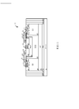
- FIG. 1 shows an example embodiment 10 of a p-type LDMOS.
- the LDMOS is formed on an n-type wafer (e.g., an n-wafer) 12.
- a bulk oxide (e.g., box) 14 is formed on the n-wafer 12.
- An oxide 16 encloses a vertical n-type shield 15.
- An n-type buried layer (e.g., nbl) 20 is formed on the box 14.
- the box 14 and the n-typed shield 15 form a shielded region, within which transistors are formed.
- a p-type epitaxial layer (e.g., p-epi) 22 is formed on the nbl 20.
- N-type high voltage implants e.g., nhv 24 are formed over the nbl 20 to form a respective body region for each of two transistors included in the embodiment 10.
- a p-type high voltage p-well e.g., hvpw
- An STI 28 is formed between a body contact 40 of each respective transistor and the n-type shield 18.
- the body contact 40 forms a low impedance connection to the nhv 24.
- a source contact 42 abuts the body contact 40.
- a pair of p-type extension implants (e.g., pext) 44 are formed adjacent to the source contact 42.
- An STI 50 is formed in the hvpw 26 drift region for each respective transistor.
- a shared drain contact 52 is formed in the hvpw 26.
- a polysilicon gate 54 is formed over the STI 50 and a channel region 56 for each respective transistor.
- a spacer 58 is formed laterally on either side of the polysilicon gate 54 for each respective transistor.
- a silicide 60 is formed over the butted body contact 40 and source contact 42 for each respective transistor. The silicide 60 is also formed over each polysilicon gate 54 and the shared drain contact 60.
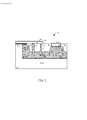
- FIG. 2 shows a portion 70 of the embodiment 10 of FIG. 1 , including defects in the STI 50.
- a needle defect 72 extends from the hvpw 26, thus creating a reduction in the vertical separation 74 of the hvpw 26 and the gate electrode 54.
- the hvpw 26 and the gate electrode are biased to different potentials, hence the reduced vertical separation 74 causes undesirable leakage therebetween.
- the reduction in the vertical separation 74 results in an oxide breakdown between the needle defect 72 and the gate electrode 54.
- FIG. 2 further shows a pillar defect 76 extending to the surface of the STI 50, and a needle defect 78 on a sidewall of the STI 50.
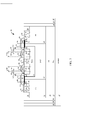
- FIG. 3 shows an example embodiment 80 of a p-type LDMOS with a split gate configuration and a mask for reducing transistor sensitivity to STI defects in accordance with the present disclosure.
- the embodiment 80 includes a first polysilicon gate electrode 82 separate from a second polysilicon gate electrode 84.
- the first polysilicon gate electrode 82 is formed over a channel region 86 and controls the formation and conduction of the channel region 86.
- the second polysilicon gate electrode 84 is formed over an isolation region (e.g., an STI 50), and forms a field plate with the drift region in the hvpw 26.
- an isolation region e.g., an STI 50
- a spacer 88 is formed laterally on either side of the first polysilicon gate 82 and the second polysilicon gate 84 for each respective transistor.
- a silicide 90 is formed over the butted body contact 40 and source contact 42 for each respective transistor. The silicide 90 is also formed over each polysilicon gate 82, 84 and the shared drain contact 52.
- a respective mask 100 defines an area within each of the STI 50 regions for further processing.
- the first polysilicon gate electrode 82 is separated from the STI edge by a distance 102.
- the mask 100 is separated from the STI edge by a first distance 104, and from the second polysilicon electrode 84 by a second distance 106. It should be appreciated that a similarly constrained separation of the mask 100 as shown by the first distance 104 and the second distance 106 applies to both respective STI edges and both respective edges of the second polysilicon electrode 84.
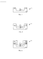
- FIGs. 4 through FIG. 9 show a sequence of fabrication stages of a semiconductor device 110 using a novel method to reduce a transistor sensitivity to an STI defect.
- FIG. 4 shows an early stage of STI formation, similar to that used to form the STI 50 of FIG. 3 .
- a Silicon substrate 112 is patterned with a Silicon Nitride layer (114). The opening defined by the Silicon Nitride layer 114 is used to etch a trench in the substrate 112. Due to particles or other impurities on the substrate 112, a region in the trench is blocked from being fully etched. Accordingly, the blocked etch forms a needle defect 116.
- a High Density Plasma (HDP) oxide 118 is deposited to partially fill the trench.
- HDP High Density Plasma
- a photo resist mask 120 is deposited and patterned to open a planar area, within the planar area defined by the STI trench sidewalls.
- the photo resist mask is replaced with another type of mask, not limited by photolithography.
- the HDP oxide 118 is etched to remove the oxide coating 122 of the pillar 116, thereby exposing a top portion 124 of the needle defect 116.
- a polysilicon etch step reduces the top portion 124 of the needle defect 116 to a reduced height 126.
- the embodiment 110 of FIG. 7 uses a polysilicon etch step to reduce a height of a silicon-based needle defect 116. It should be appreciated that other embodiments comprising a defect based on a material other than silicon will use the appropriate type of semiconductor etch method to achieve a similar reduction in the height of the needle defect 116.
- the photo resist mask 120 is removed.
- the trench is at least partially filled with an oxide 130, to complete the STI formation, similar to the STI 50 of FIG. 3 .
- FIG. 10 with reference to FIG.
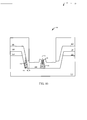
- FIG. 7 shows a fabrication stage of a semiconductor device having two needle defects in the etched trench.
- the needle defect 142 is on a sidewall of the STI and unable to be etched back with the etch step shown in FIG. 7 .
- the photo resist mask 120 will overlap the needle defect 142 by a distance 144, thereby blocking the etch back of the needle defect 142.
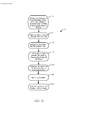
- FIG. 11 shows a method 150 for manufacturing a semiconductor device in accordance with an example embodiment of the present disclosure.
- a first gate electrode 82 is formed over a channel region 86.
- a second gate electrode 84 is formed over an isolation region (e.g., an STI 50).
- a trench is formed in a substrate 26, including a defect (e.g., a needle, cone or pillar defect).
- an area within the trench is defined (e.g., with a mask 100).
- the trench is, at least partially, filled with an oxide.
- the oxide is, at least partially, removed to expose a top portion of the defect.
- the top portion of the defect is removed with a semiconductor etch (e.g., a silicon etch when the defect comprises silicon).
- the trench is, at least partially, filled with an oxide.
- FIG. 12 shows a method 170 for manufacturing a semiconductor device in accordance with an example embodiment of the present disclosure.
- a trench including a defect is formed in a substrate 26, wherein the trench defines an isolation region (e.g., an STI 50), including a gate electrode 84 disposed thereon.
- the trench is, at least partially, filled with an oxide.
- an area is defined with the trench with a mask 100.
- the oxide is, at least partially, removed to expose a top portion of the defect.
- the top portion of the defect is removed with a semiconductor etch.
- the mask is removed.
- the trench is, at least partially, filled with an oxide.
- FIG. 13 shows a method 190 for manufacturing a semiconductor device in accordance with an example embodiment of the present disclosure.
- a trench in a substrate is filled, at least partially, with an oxide, wherein the trench defines an STI (e.g. an STI 50), including a defect.
- an area within the trench is defined with a mask 100.
- the oxide is, at least partially, removed to expose the top portion of the defect.
- the top portion of the defect is removed with a semiconductor etch.
- the mask 100 is removed.
- the trench is, at least partially, filled with an oxide.
- a field plate of a split gate transistor is formed over the STI.
- a method for manufacturing a semiconductor device comprises forming a first gate electrode over a channel region.
- a second gate electrode is formed over an isolation region, wherein the first gate electrode is laterally separated from the isolation region, and the isolation region is formed by performing the steps of forming a trench in a substrate of the semiconductor device, the trench defining a first planar area of the isolation region and comprising a defect; defining with a mask, a second planar area within the first planar area comprising a first lateral distance between an edge of the mask and an edge of the isolation region, and a second lateral distance between the edge of the mask and an edge of the second gate electrode; filling the trench, at least partially, with a first oxide; removing, at least partially, the first oxide with an oxide etch to expose a top portion of the defect; removing the top portion of the defect with a semiconductor etch, thereby increasing a vertical separation between the second gate electrode and the defect; and after removing the top portion
- the first lateral distance exceeds a threshold value to prevent the semiconductor etch from etching a sidewall of the trench.
- the first lateral distance is less than a threshold value to reduce a number of defects blocked from being etched by the semiconductor etch.
- the second lateral distance is less than a threshold value to reduce a breakdown voltage of the semiconductor device.
- the trench is completely filled with the second oxide prior to forming the second gate electrode.
- the isolation region is a shallow trench isolation region.
- the semiconductor device is a p-type high voltage transistor.
- the semiconductor device is an n-type high voltage transistor.
- the first oxide is a high density plasma oxide.
- the mask defines a respective isolation region of two semiconductor devices sharing a common drain contact disposed therebetween.
- the defect is one of a needle defect, a cone defect and a pillar defect.
- a method for manufacturing an isolation region comprises forming a trench in a substrate of a semiconductor device, the trench defining a first planar area of an isolation region, the trench comprising a defect and the isolation region comprising a gate electrode disposed thereon.
- the trench is filled, at least partially, with a first oxide.
- a mask defines a second planar area within the first planar area comprising a first lateral distance between an edge of the mask and an edge of the isolation region, and a second lateral distance between the edge of the mask and an edge of the gate electrode.
- the first oxide beneath the second planar area is at least partially removed, with an oxide etch to expose a top portion of the defect.
- the top portion of the defect is removed with a semiconductor etch, thereby increasing a vertical separation between the second gate electrode and the defect.
- the trench is at least partially filled with a second oxide.
- the first lateral distance exceeds a threshold value to prevent the semiconductor etch from etching a sidewall of the trench.
- the first lateral distance is less than a threshold value to reduce a number of defects blocked from being etched by the semiconductor etch.
- the second lateral distance is less than a threshold value to reduce a breakdown voltage of the semiconductor device.
- the first oxide is a high density plasma oxide.
- the defect is one of a needle defect, a cone defect and a pillar defect.
- a method for reducing transistor sensitivity to STI defects comprises filling a trench formed in a substrate of a semiconductor device, at least partially, with a first oxide, the trench defining an STI and comprising a defect extending from the substrate.
- a mask defines a planar area within the isolation region comprising a first lateral distance between an edge of the photo resist mask and an edge of the isolation region.
- the first oxide beneath the planar area is at least partially removed with an oxide etch to expose a top portion of the defect.
- the top portion of the defect is removed with a semiconductor etch.
- the trench is at least partially filled with a second oxide.
- a field plate of a split-gate transistor is formed over the STI.
- the first lateral distance exceeds a threshold value to prevent the semiconductor etch from etching a sidewall of the trench.
- the first lateral distance is less than a threshold value to reduce a number of defects blocked from being etched by the semiconductor etch.
- a first width of the photo resist mask reduced by a second width of the field plate is less than a threshold value to reduce a breakdown voltage of the split-gate transistor.
Landscapes
- Insulated Gate Type Field-Effect Transistor (AREA)
- Element Separation (AREA)
- Engineering & Computer Science (AREA)
- Manufacturing & Machinery (AREA)
Abstract
A method for reducing transistor sensitivity to shallow trench isolation defects (STI) includes filling a trench formed in a substrate of a semiconductor device, at least partially, with a first oxide, the trench defines an STI and includes a defect extending from the substrate. A mask defines a planar area within the isolation region including a first lateral distance between an edge of the mask and an edge of the isolation region. The first oxide is at least partially removed beneath the planar area with an oxide etch to expose a top portion of the defect. The top portion of the defect is removed with a semiconductor etch. After removing the top portion of the defect, the trench is at least partially filled with a second oxide. A field plate of a split-gate transistor is formed over the STI.
Description
- This disclosure relates generally to a manufacturing process for a high voltage semiconductor device, and more specifically to reducing a sensitivity of a high voltage transistor to a defect in an isolation region of the semiconductor device.
- Shallow Trench Isolation (STI) regions are typically used to form high voltage semiconductor devices. The formation of an STI includes forming a trench in a silicon substrate and thermally oxidizing the trench to form a silicon oxide layer. Due to inherent particulate on the substrate during fabrication of the STI, certain areas of the trench may not be fully etched, thus resulting in defects. In one example, the incomplete etch results in a needle defect extending vertically from the bottom of the trench.
- Subsequently, the trench is filled with an oxide and a gate electrode is deposited over the region including the defect. The defect is biased to the same potential as the silicon substrate, from which it extends. Accordingly, electrical breakdown between the defect and the gate electrode may occur due to the reduced separation between the defect and the gate electrode. Mitigating the effects of the defect has traditionally being problematic due to the tight physical tolerances between the defect, the gate electrode and various active areas of the semiconductor device.
- The present invention is illustrated by way of example and is not limited by the accompanying figures, in which like references indicate similar elements. Elements in the figures are illustrated for simplicity and clarity and have not necessarily been drawn to scale.
-
FIG. 1 is a cross-sectional view of an example embodiment of a p-type Laterally Diffused Metal Oxide Semiconductor (LDMOS). -
FIG. 2 is a cross-sectional view of a formation of a trench with defects during a fabrication stage of the LDMOS ofFIG. 1 . -
FIG. 3 is a cross-sectional view of a split-gate transistor with a mask for reducing a transistor sensitivity to a defect in an STI, in accordance with an example embodiment of the present disclosure. -
FIG. 4 is a cross-sectional view of a fabrication stage of a semiconductor device including the reduction of the transistor sensitivity to the STI defect, in accordance with an example embodiment of the present disclosure. -
FIG. 5 is a cross-sectional view of a fabrication stage of a semiconductor device including the reduction of the transistor sensitivity to the STI defect, in accordance with an example embodiment of the present disclosure. -
FIG. 6 is a cross-sectional view of a fabrication stage of a semiconductor device including the reduction of the transistor sensitivity to the STI defect, in accordance with an example embodiment of the present disclosure. -
FIG. 7 is a cross-sectional view of a fabrication stage of a semiconductor device including the reduction of the transistor sensitivity to the STI defect, in accordance with an example embodiment of the present disclosure. -
FIG. 8 is a cross-sectional view of a fabrication stage of a semiconductor device including the reduction of the transistor sensitivity to the STI defect, in accordance with an example embodiment of the present disclosure. -
FIG. 9 is a cross-sectional view of a fabrication stage of a semiconductor device including the reduction of the transistor sensitivity to the STI defect, in accordance with an example embodiment of the present disclosure. -
FIG. 10 is a cross-sectional view of a fabrication stage of a semiconductor device as shown inFIG. 8 with a defect unable to be reduced due to mask blockage. -
FIG. 11 is a flowchart representation of a method for manufacturing a semiconductor device in accordance with an example embodiment of the present disclosure. -
FIG. 12 is a flowchart representation of a method for manufacturing an isolation region in accordance with an example embodiment of the present disclosure. -
FIG. 13 is a flowchart representation of a method for reducing transistor sensitivity to STI defects in accordance with an example embodiment of the present disclosure. - Embodiments described herein provide for methods for reducing the sensitivity of a high voltage transistor to STI defects in a semiconductor process. During the formation of the STI, defects may occur as a result of blocked etching of the STI. In example embodiments, the defect is a needle defect, a cone defect or a pillar defect, although other defect types extending from the underlying silicon layer of an STI are envisioned within the scope of this disclosure.
- These defects reduce a thickness of an oxide layer between one of the defects and a subsequently formed, overlying polysilicon gate. Consequently, a leakage path, (or in some embodiments, a dielectric breakdown), occurs between the defect and the gate, which reduces the performance, reliability or yield of the semiconductor device including the transistor. The sensitivity of the transistor to such defects is improved by reducing a height of the defects, thereby increasing the oxide layer thickness between the defect and the overlying gate.
- Reducing the defect height is achieved by using a mask to define an area within the STI for exposing and partially etching back the defect. This mask requires tightly controlled spacing with respect to the overlying polysilicon gate and also with respect to an edge of the STI. The mask must have sufficient separation from the STI edge to prevent etching damage to the STI sidewall. Conversely, the separation of the mask from the STI edge must be sufficiently small to reduce a number of defects that will not be subject to the defect height reduction methods described herein. The mask separation from the nearest edge of the polysilicon gate must also be sufficiently small to minimize a breakdown voltage of the transistor.
- Embodiments described herein, include a split gate transistor configuration, which includes a first polysilicon gate electrode over a channel region on the substrate, and a second polysilicon gate electrode over an isolation region (e.g., an STI) to form a field plate to bias an underlying drift region. The aforementioned critical mask spacing and alignment are alleviated with a split gate transistor configuration, and the defect height reduction methods described in this disclosure, effectively reduce the transistor sensitivity to defects in the isolation region, or STI.
-
FIG. 1 shows anexample embodiment 10 of a p-type LDMOS. The LDMOS is formed on an n-type wafer (e.g., an n-wafer) 12. A bulk oxide (e.g., box) 14 is formed on the n-wafer 12. Anoxide 16 encloses a vertical n-type shield 15. An n-type buried layer (e.g., nbl) 20 is formed on thebox 14. Thebox 14 and the n-typed shield 15 form a shielded region, within which transistors are formed. A p-type epitaxial layer (e.g., p-epi) 22 is formed on thenbl 20. N-type high voltage implants (e.g., nhv) 24 are formed over thenbl 20 to form a respective body region for each of two transistors included in theembodiment 10. A p-type high voltage p-well (e.g., hvpw) 26 is formed in the p-epi 22. AnSTI 28 is formed between abody contact 40 of each respective transistor and the n-type shield 18. Thebody contact 40 forms a low impedance connection to thenhv 24. Asource contact 42 abuts thebody contact 40. A pair of p-type extension implants (e.g., pext) 44 are formed adjacent to thesource contact 42. - An STI 50 is formed in the
hvpw 26 drift region for each respective transistor. A shareddrain contact 52 is formed in the hvpw 26. Apolysilicon gate 54 is formed over theSTI 50 and achannel region 56 for each respective transistor. Aspacer 58 is formed laterally on either side of thepolysilicon gate 54 for each respective transistor. Asilicide 60 is formed over the buttedbody contact 40 andsource contact 42 for each respective transistor. Thesilicide 60 is also formed over eachpolysilicon gate 54 and the shareddrain contact 60. -
FIG. 2 shows aportion 70 of theembodiment 10 ofFIG. 1 , including defects in theSTI 50. Aneedle defect 72 extends from thehvpw 26, thus creating a reduction in thevertical separation 74 of thehvpw 26 and thegate electrode 54. Thehvpw 26 and the gate electrode are biased to different potentials, hence the reducedvertical separation 74 causes undesirable leakage therebetween. In one embodiment, the reduction in thevertical separation 74 results in an oxide breakdown between theneedle defect 72 and thegate electrode 54.FIG. 2 further shows apillar defect 76 extending to the surface of theSTI 50, and aneedle defect 78 on a sidewall of theSTI 50. -
FIG. 3 shows anexample embodiment 80 of a p-type LDMOS with a split gate configuration and a mask for reducing transistor sensitivity to STI defects in accordance with the present disclosure. In contrast to theembodiment 10 ofFIG. 1 , theembodiment 80 includes a firstpolysilicon gate electrode 82 separate from a secondpolysilicon gate electrode 84. The firstpolysilicon gate electrode 82 is formed over achannel region 86 and controls the formation and conduction of thechannel region 86. The secondpolysilicon gate electrode 84 is formed over an isolation region (e.g., an STI 50), and forms a field plate with the drift region in thehvpw 26. Aspacer 88 is formed laterally on either side of thefirst polysilicon gate 82 and thesecond polysilicon gate 84 for each respective transistor. Asilicide 90 is formed over the buttedbody contact 40 andsource contact 42 for each respective transistor. Thesilicide 90 is also formed over eachpolysilicon gate drain contact 52. - In the
embodiment 80, arespective mask 100 defines an area within each of theSTI 50 regions for further processing. In theembodiment 80, the firstpolysilicon gate electrode 82 is separated from the STI edge by adistance 102. Themask 100 is separated from the STI edge by afirst distance 104, and from thesecond polysilicon electrode 84 by asecond distance 106. It should be appreciated that a similarly constrained separation of themask 100 as shown by thefirst distance 104 and thesecond distance 106 applies to both respective STI edges and both respective edges of thesecond polysilicon electrode 84. -
FIGs. 4 through FIG. 9 show a sequence of fabrication stages of asemiconductor device 110 using a novel method to reduce a transistor sensitivity to an STI defect.FIG. 4 shows an early stage of STI formation, similar to that used to form theSTI 50 ofFIG. 3 . ASilicon substrate 112, is patterned with a Silicon Nitride layer (114). The opening defined by theSilicon Nitride layer 114 is used to etch a trench in thesubstrate 112. Due to particles or other impurities on thesubstrate 112, a region in the trench is blocked from being fully etched. Accordingly, the blocked etch forms aneedle defect 116. As shown inFIG. 5 , a High Density Plasma (HDP)oxide 118 is deposited to partially fill the trench. As shown inFIG. 6 , a photo resistmask 120 is deposited and patterned to open a planar area, within the planar area defined by the STI trench sidewalls. In another embodiment, the photo resist mask is replaced with another type of mask, not limited by photolithography. Using the photo resistmask 120 to define the planar area, theHDP oxide 118 is etched to remove theoxide coating 122 of thepillar 116, thereby exposing atop portion 124 of theneedle defect 116. - As shown in
FIG. 7 , a polysilicon etch step reduces thetop portion 124 of theneedle defect 116 to a reducedheight 126. Theembodiment 110 ofFIG. 7 uses a polysilicon etch step to reduce a height of a silicon-basedneedle defect 116. It should be appreciated that other embodiments comprising a defect based on a material other than silicon will use the appropriate type of semiconductor etch method to achieve a similar reduction in the height of theneedle defect 116. As shown inFIG. 8 , the photo resistmask 120 is removed. As shown inFIG. 9 , the trench is at least partially filled with anoxide 130, to complete the STI formation, similar to theSTI 50 ofFIG. 3 .FIG. 10 , with reference toFIG. 7 , shows a fabrication stage of a semiconductor device having two needle defects in the etched trench. In contrast to theneedle defect 116, theneedle defect 142 is on a sidewall of the STI and unable to be etched back with the etch step shown inFIG. 7 . Specifically, when thefirst distance 104 shown inFIG. 3 , between the mask and the STI edge is too large, the photo resistmask 120 will overlap theneedle defect 142 by adistance 144, thereby blocking the etch back of theneedle defect 142. -
FIG. 11 , with reference toFIG. 3 , shows amethod 150 for manufacturing a semiconductor device in accordance with an example embodiment of the present disclosure. At 152, afirst gate electrode 82 is formed over achannel region 86. At 154, asecond gate electrode 84 is formed over an isolation region (e.g., an STI 50). At 156, a trench is formed in asubstrate 26, including a defect (e.g., a needle, cone or pillar defect). At 158, an area within the trench is defined (e.g., with a mask 100). At 160, the trench is, at least partially, filled with an oxide. At 162, the oxide is, at least partially, removed to expose a top portion of the defect. At 164, the top portion of the defect is removed with a semiconductor etch (e.g., a silicon etch when the defect comprises silicon). At 166, the trench is, at least partially, filled with an oxide. -
FIG. 12 , with reference toFIG. 3 , shows amethod 170 for manufacturing a semiconductor device in accordance with an example embodiment of the present disclosure. At 172, a trench including a defect is formed in asubstrate 26, wherein the trench defines an isolation region (e.g., an STI 50), including agate electrode 84 disposed thereon. At 174, the trench is, at least partially, filled with an oxide. At 176, an area is defined with the trench with amask 100. At 178, the oxide is, at least partially, removed to expose a top portion of the defect. At 180, the top portion of the defect is removed with a semiconductor etch. At 182, the mask is removed. At 184, the trench is, at least partially, filled with an oxide. -
FIG. 13 , with reference toFIG. 3 , shows amethod 190 for manufacturing a semiconductor device in accordance with an example embodiment of the present disclosure. At 192, a trench in a substrate is filled, at least partially, with an oxide, wherein the trench defines an STI (e.g. an STI 50), including a defect. At 194, an area within the trench is defined with amask 100. At 196, the oxide is, at least partially, removed to expose the top portion of the defect. At 198, the top portion of the defect is removed with a semiconductor etch. At 200, themask 100 is removed. At 202, the trench is, at least partially, filled with an oxide. At 204, a field plate of a split gate transistor is formed over the STI. - As will be appreciated, embodiments as disclosed include at least the following. In one embodiment, a method for manufacturing a semiconductor device comprises forming a first gate electrode over a channel region. A second gate electrode is formed over an isolation region, wherein the first gate electrode is laterally separated from the isolation region, and the isolation region is formed by performing the steps of forming a trench in a substrate of the semiconductor device, the trench defining a first planar area of the isolation region and comprising a defect; defining with a mask, a second planar area within the first planar area comprising a first lateral distance between an edge of the mask and an edge of the isolation region, and a second lateral distance between the edge of the mask and an edge of the second gate electrode; filling the trench, at least partially, with a first oxide; removing, at least partially, the first oxide with an oxide etch to expose a top portion of the defect; removing the top portion of the defect with a semiconductor etch, thereby increasing a vertical separation between the second gate electrode and the defect; and after removing the top portion of the defect, filling the trench, at least partially, with a second oxide.
- Alternative embodiments of the method for manufacturing a semiconductor device include one of the following features, or any combination thereof. The first lateral distance exceeds a threshold value to prevent the semiconductor etch from etching a sidewall of the trench. The first lateral distance is less than a threshold value to reduce a number of defects blocked from being etched by the semiconductor etch. The second lateral distance is less than a threshold value to reduce a breakdown voltage of the semiconductor device. The trench is completely filled with the second oxide prior to forming the second gate electrode. The isolation region is a shallow trench isolation region. The semiconductor device is a p-type high voltage transistor. The semiconductor device is an n-type high voltage transistor. The first oxide is a high density plasma oxide. The mask defines a respective isolation region of two semiconductor devices sharing a common drain contact disposed therebetween. The defect is one of a needle defect, a cone defect and a pillar defect.
- In another embodiment, a method for manufacturing an isolation region comprises forming a trench in a substrate of a semiconductor device, the trench defining a first planar area of an isolation region, the trench comprising a defect and the isolation region comprising a gate electrode disposed thereon. The trench is filled, at least partially, with a first oxide. A mask defines a second planar area within the first planar area comprising a first lateral distance between an edge of the mask and an edge of the isolation region, and a second lateral distance between the edge of the mask and an edge of the gate electrode. The first oxide beneath the second planar area is at least partially removed, with an oxide etch to expose a top portion of the defect. The top portion of the defect is removed with a semiconductor etch, thereby increasing a vertical separation between the second gate electrode and the defect. After removing the top portion of the defect, the trench is at least partially filled with a second oxide.
- Alternative embodiments of the method for manufacturing an isolation region include one of the following features, or any combination thereof. The first lateral distance exceeds a threshold value to prevent the semiconductor etch from etching a sidewall of the trench. The first lateral distance is less than a threshold value to reduce a number of defects blocked from being etched by the semiconductor etch. The second lateral distance is less than a threshold value to reduce a breakdown voltage of the semiconductor device. The first oxide is a high density plasma oxide. The defect is one of a needle defect, a cone defect and a pillar defect.
- In another embodiment, a method for reducing transistor sensitivity to STI defects comprises filling a trench formed in a substrate of a semiconductor device, at least partially, with a first oxide, the trench defining an STI and comprising a defect extending from the substrate. A mask defines a planar area within the isolation region comprising a first lateral distance between an edge of the photo resist mask and an edge of the isolation region. The first oxide beneath the planar area is at least partially removed with an oxide etch to expose a top portion of the defect. The top portion of the defect is removed with a semiconductor etch. After removing the top portion of the defect, the trench is at least partially filled with a second oxide. A field plate of a split-gate transistor is formed over the STI.
- Alternative embodiments of the method for reducing transistor sensitivity to STI defects include one of the following features, or any combination thereof. The first lateral distance exceeds a threshold value to prevent the semiconductor etch from etching a sidewall of the trench. The first lateral distance is less than a threshold value to reduce a number of defects blocked from being etched by the semiconductor etch. A first width of the photo resist mask reduced by a second width of the field plate is less than a threshold value to reduce a breakdown voltage of the split-gate transistor.
- Although the invention is described herein with reference to specific embodiments, various modifications and changes can be made without departing from the scope of the present invention as set forth in the claims below. Accordingly, the specification and figures are to be regarded in an illustrative rather than a restrictive sense, and all such modifications are intended to be included within the scope of the present invention. Any benefits, advantages, or solutions to problems that are described herein with regard to specific embodiments are not intended to be construed as a critical, required, or essential feature or element of any or all the claims.
- Unless stated otherwise, terms such as "first" and "second" are used to arbitrarily distinguish between the elements such terms describe. Thus, these terms are not necessarily intended to indicate temporal or other prioritization of such elements.
- The present disclosure extends to the following series of lettered clauses:
- A method for manufacturing an isolation region comprising: forming a trench in a substrate of a semiconductor device, the trench defining a first planar area of an isolation region, the trench comprising a defect and the isolation region comprising a gate electrode disposed thereon; filling the trench, at least partially, with a first oxide; defining with a mask, a second planar area within the first planar area comprising a first lateral distance between an edge of the mask and an edge of the isolation region, and a second lateral distance between the edge of the mask and an edge of the gate electrode; removing, at least partially, the first oxide beneath the second planar area, with an oxide etch to expose a top portion of the defect; removing the top portion of the defect with a semiconductor etch, thereby increasing a vertical separation between the second gate electrode and the defect; and after removing the top portion of the defect, filling the trench, at least partially, with a second oxide.
- B. A method for reducing transistor sensitivity to shallow trench isolation (STI) defects comprising: filling a trench formed in a substrate of a semiconductor device, at least partially, with a first oxide, the trench defining an STI and comprising a defect extending from the substrate; defining with a mask, a planar area within the isolation region comprising a first lateral distance between an edge of the photo resist mask and an edge of the isolation region; removing, at least partially, the first oxide beneath the planar area with an oxide etch to expose a top portion of the defect; removing the top portion of the defect with a semiconductor etch; after removing the top portion of the defect, filling the trench, at least partially, with a second oxide; and forming a field plate of a split-gate transistor over the STI.
- C. The method of clause A or B wherein the first lateral distance exceeds a threshold value to prevent the semiconductor etch from etching a sidewall of the trench.
- D. The method of clause A, B or C wherein the first lateral distance is less than a threshold value to reduce a number of defects blocked from being etched by the semiconductor etch.
- E. The method of any of clauses A to D wherein the second lateral distance is less than a threshold value to reduce a breakdown voltage of the semiconductor device.
- F. The method of any of clauses A to E wherein the first oxide is a high density plasma oxide.
- G. The method of any of clauses A to F wherein the defect is one of a needle defect, a cone defect and a pillar defect.
- H. The method of clause B wherein a first width of the photo resist mask reduced by a second width of the field plate is less than a threshold value to reduce a breakdown voltage of the split-gate transistor.
Claims (10)
- A method for manufacturing a semiconductor device comprising:forming a first gate electrode over a channel region; andforming a second gate electrode over an isolation region, wherein the first gate electrode is laterally separated from the isolation region, and the isolation region is formed by performing the steps of:forming a trench in a substrate of the semiconductor device, the trench defining a first planar area of the isolation region and comprising a defect,defining with a mask, a second planar area within the first planar area comprising a first lateral distance between an edge of the mask and an edge of the isolation region, and a second lateral distance between the edge of the mask and an edge of the second gate electrode,filling the trench, at least partially, with a first oxide,removing, at least partially, the first oxide with an oxide etch to expose a top portion of the defect,removing the top portion of the defect with a semiconductor etch, thereby increasing a vertical separation between the second gate electrode and the defect, andafter removing the top portion of the defect, filling the trench, at least partially, with a second oxide.
- The method of claim 1 wherein the first lateral distance exceeds a threshold value to prevent the semiconductor etch from etching a sidewall of the trench.
- The method of claim 1 or 2 wherein the first lateral distance is less than a threshold value to reduce a number of defects blocked from being etched by the semiconductor etch.
- The method of any preceding claim wherein the second lateral distance is less than a threshold value to reduce a breakdown voltage of the semiconductor device.
- The method of any preceding claim further comprising completely filling the trench with the second oxide prior to forming the second gate electrode.
- The method of any preceding claim wherein the isolation region is a shallow trench isolation region.
- The method of any preceding claim wherein the semiconductor device is a p-type high voltage transistor.
- The method of any preceding claim wherein the semiconductor device is an n-type high voltage transistor.
- The method of any preceding claim wherein the first oxide is a high density plasma oxide.
- The method of any preceding claim wherein the defect is one of a needle defect, a cone defect and a pillar defect.
Applications Claiming Priority (1)
| Application Number | Priority Date | Filing Date | Title |
|---|---|---|---|
| US16/505,994 US10825717B1 (en) | 2019-07-09 | 2019-07-09 | Method for making high voltage transistors insensitive to needle defects in shallow trench isolation |
Publications (1)
| Publication Number | Publication Date |
|---|---|
| EP3764391A1 true EP3764391A1 (en) | 2021-01-13 |
Family
ID=71401577
Family Applications (1)
| Application Number | Title | Priority Date | Filing Date |
|---|---|---|---|
| EP20182796.1A Withdrawn EP3764391A1 (en) | 2019-07-09 | 2020-06-29 | Method for making high voltage transistors insensitive to needle defects in shallow trench isolation |
Country Status (4)
| Country | Link |
|---|---|
| US (1) | US10825717B1 (en) |
| EP (1) | EP3764391A1 (en) |
| CN (1) | CN112216611A (en) |
| TW (1) | TW202117929A (en) |
Cited By (3)
| Publication number | Priority date | Publication date | Assignee | Title |
|---|---|---|---|---|
| CN115132646A (en) * | 2021-03-29 | 2022-09-30 | 世界先进积体电路股份有限公司 | Method for forming semiconductor device |
| WO2022241064A1 (en) * | 2021-05-13 | 2022-11-17 | Texas Instruments Incorporated | Shallow trench isolation processing with local oxidation of silicon |
| US12199091B2 (en) | 2021-05-13 | 2025-01-14 | Texas Instruments Incorporated | Shallow trench isolation processing with local oxidation of silicon |
Families Citing this family (2)
| Publication number | Priority date | Publication date | Assignee | Title |
|---|---|---|---|---|
| US11411495B2 (en) * | 2020-06-23 | 2022-08-09 | Tower Semiconductor Ltd. | Apparatus, system and method of a metal-oxide-semiconductor (MOS) transistor including a split-gate structure |
| CN115083918B (en) * | 2022-07-19 | 2022-11-04 | 合肥晶合集成电路股份有限公司 | Transistor and method of making the same |
Citations (3)
| Publication number | Priority date | Publication date | Assignee | Title |
|---|---|---|---|---|
| US20140312417A1 (en) * | 2013-04-17 | 2014-10-23 | Infineon Technologies Dresden Gmbh | Semiconductor Device and Method of Manufacturing a Semiconductor Device |
| US8969958B1 (en) * | 2009-11-13 | 2015-03-03 | Maxim Integrated Products, Inc. | Integrated MOS power transistor with body extension region for poly field plate depletion assist |
| US9105687B1 (en) * | 2014-04-16 | 2015-08-11 | Nxp B.V. | Method for reducing defects in shallow trench isolation |
Family Cites Families (8)
| Publication number | Priority date | Publication date | Assignee | Title |
|---|---|---|---|---|
| US6080677A (en) | 1997-06-17 | 2000-06-27 | Vlsi Technology, Inc. | Method for preventing micromasking in shallow trench isolation process etching |
| US6825544B1 (en) * | 1998-12-09 | 2004-11-30 | Cypress Semiconductor Corporation | Method for shallow trench isolation and shallow trench isolation structure |
| US6277752B1 (en) | 1999-06-28 | 2001-08-21 | Taiwan Semiconductor Manufacturing Company | Multiple etch method for forming residue free patterned hard mask layer |
| US6194284B1 (en) | 1999-08-30 | 2001-02-27 | Taiwan Semiconductor Manufacturing Company | Method for forming residue free etched silicon layer |
| US6281093B1 (en) | 2000-07-19 | 2001-08-28 | Chartered Semiconductor Manufacturing Ltd. | Method to reduce trench cone formation in the fabrication of shallow trench isolations |
| US20020182852A1 (en) | 2001-05-03 | 2002-12-05 | Koninklijke Philips Electronics N.V. | Method for reducing micro-masking defects in trench isolation regions |
| US7635614B1 (en) | 2007-03-15 | 2009-12-22 | National Semiconductor Corporation | Double gate NLDMOS SCR device with controllable switching characteristics |
| US8247869B2 (en) | 2010-04-26 | 2012-08-21 | Freescale Semiconductor, Inc. | LDMOS transistors with a split gate |
-
2019
- 2019-07-09 US US16/505,994 patent/US10825717B1/en active Active
-
2020
- 2020-04-22 TW TW109113505A patent/TW202117929A/en unknown
- 2020-06-29 EP EP20182796.1A patent/EP3764391A1/en not_active Withdrawn
- 2020-07-08 CN CN202010651693.6A patent/CN112216611A/en active Pending
Patent Citations (3)
| Publication number | Priority date | Publication date | Assignee | Title |
|---|---|---|---|---|
| US8969958B1 (en) * | 2009-11-13 | 2015-03-03 | Maxim Integrated Products, Inc. | Integrated MOS power transistor with body extension region for poly field plate depletion assist |
| US20140312417A1 (en) * | 2013-04-17 | 2014-10-23 | Infineon Technologies Dresden Gmbh | Semiconductor Device and Method of Manufacturing a Semiconductor Device |
| US9105687B1 (en) * | 2014-04-16 | 2015-08-11 | Nxp B.V. | Method for reducing defects in shallow trench isolation |
Cited By (3)
| Publication number | Priority date | Publication date | Assignee | Title |
|---|---|---|---|---|
| CN115132646A (en) * | 2021-03-29 | 2022-09-30 | 世界先进积体电路股份有限公司 | Method for forming semiconductor device |
| WO2022241064A1 (en) * | 2021-05-13 | 2022-11-17 | Texas Instruments Incorporated | Shallow trench isolation processing with local oxidation of silicon |
| US12199091B2 (en) | 2021-05-13 | 2025-01-14 | Texas Instruments Incorporated | Shallow trench isolation processing with local oxidation of silicon |
Also Published As
| Publication number | Publication date |
|---|---|
| CN112216611A (en) | 2021-01-12 |
| US10825717B1 (en) | 2020-11-03 |
| TW202117929A (en) | 2021-05-01 |
Similar Documents
| Publication | Publication Date | Title |
|---|---|---|
| US10825717B1 (en) | Method for making high voltage transistors insensitive to needle defects in shallow trench isolation | |
| US11081558B2 (en) | LDMOS with high-k drain STI dielectric | |
| US9673289B2 (en) | Dual oxide trench gate power MOSFET using oxide filled trench | |
| US20160172245A1 (en) | Method of forming a Gate Shield in an ED-CMOS Transistor and a base of a bipolar transistor using BICMOS Technologies | |
| CN105990374B (en) | Integrated circuit and method for manufacturing transistor | |
| US10014206B1 (en) | Trench isolated IC with transistors having locos gate dielectric | |
| US9230956B2 (en) | Junction field effect transistors and associated fabrication methods | |
| US8525257B2 (en) | LDMOS transistor with asymmetric spacer as gate | |
| US11545398B2 (en) | Semiconductor device | |
| CN112825327A (en) | Semiconductor structure and forming method thereof | |
| CN112242305A (en) | Semiconductor device and method for manufacturing the same | |
| US6930357B2 (en) | Active SOI structure with a body contact through an insulator | |
| JP4851718B2 (en) | Semiconductor device | |
| KR102193085B1 (en) | Method to fabricate self-aligned isolation in gallium nitride devices and integrated circuits | |
| US20240347626A1 (en) | Ldmos transistor device and method for forming the same | |
| JPH0389555A (en) | Semiconductor device and manufacture thereof | |
| US20230215914A1 (en) | Semiconductor high-voltage device and manufacturing method thereof | |
| US20060046389A1 (en) | Manufacturing process and structure of integrated circuit | |
| US20140042592A1 (en) | Bipolar transistor | |
| US12328926B1 (en) | Structures for a field-effect transistor that include a spacer structure | |
| CN111681962A (en) | Shielded grid power device and its manufacturing method | |
| KR100730466B1 (en) | Trench transistor and method of manufacturing the same | |
| KR100613370B1 (en) | Semiconductor device and manufacturing method thereof | |
| US20130221444A1 (en) | Semiconductor device and manufacturing method of semiconductor device | |
| KR100490846B1 (en) | Semiconductor device and fabrication method thereof |
Legal Events
| Date | Code | Title | Description |
|---|---|---|---|
| PUAI | Public reference made under article 153(3) epc to a published international application that has entered the european phase |
Free format text: ORIGINAL CODE: 0009012 |
|
| STAA | Information on the status of an ep patent application or granted ep patent |
Free format text: STATUS: THE APPLICATION HAS BEEN PUBLISHED |
|
| AK | Designated contracting states |
Kind code of ref document: A1 Designated state(s): AL AT BE BG CH CY CZ DE DK EE ES FI FR GB GR HR HU IE IS IT LI LT LU LV MC MK MT NL NO PL PT RO RS SE SI SK SM TR |
|
| AX | Request for extension of the european patent |
Extension state: BA ME |
|
| STAA | Information on the status of an ep patent application or granted ep patent |
Free format text: STATUS: THE APPLICATION IS DEEMED TO BE WITHDRAWN |
|
| 18D | Application deemed to be withdrawn |
Effective date: 20210714 |