EP3764390A1 - Method of forming spacers of a transistor - Google Patents
Method of forming spacers of a transistor Download PDFInfo
- Publication number
- EP3764390A1 EP3764390A1 EP20185199.5A EP20185199A EP3764390A1 EP 3764390 A1 EP3764390 A1 EP 3764390A1 EP 20185199 A EP20185199 A EP 20185199A EP 3764390 A1 EP3764390 A1 EP 3764390A1
- Authority
- EP
- European Patent Office
- Prior art keywords
- layer
- portions
- basal
- thickness
- dielectric material
- Prior art date
- Legal status (The legal status is an assumption and is not a legal conclusion. Google has not performed a legal analysis and makes no representation as to the accuracy of the status listed.)
- Granted
Links
- 125000006850 spacer group Chemical group 0.000 title claims abstract description 70
- 238000000034 method Methods 0.000 title claims abstract description 44
- 238000005530 etching Methods 0.000 claims abstract description 83
- 239000003989 dielectric material Substances 0.000 claims abstract description 51
- 230000008021 deposition Effects 0.000 claims abstract description 36
- 230000004048 modification Effects 0.000 claims abstract description 35
- 238000012986 modification Methods 0.000 claims abstract description 35
- 238000002513 implantation Methods 0.000 claims description 57
- 238000000151 deposition Methods 0.000 claims description 45
- 239000000243 solution Substances 0.000 claims description 36
- 150000002500 ions Chemical class 0.000 claims description 35
- KRHYYFGTRYWZRS-UHFFFAOYSA-N Fluorane Chemical compound F KRHYYFGTRYWZRS-UHFFFAOYSA-N 0.000 claims description 31
- 239000000463 material Substances 0.000 claims description 16
- 230000008569 process Effects 0.000 claims description 14
- QPJSUIGXIBEQAC-UHFFFAOYSA-N n-(2,4-dichloro-5-propan-2-yloxyphenyl)acetamide Chemical compound CC(C)OC1=CC(NC(C)=O)=C(Cl)C=C1Cl QPJSUIGXIBEQAC-UHFFFAOYSA-N 0.000 claims description 13
- 229910052739 hydrogen Inorganic materials 0.000 claims description 12
- 239000001257 hydrogen Substances 0.000 claims description 10
- VYPSYNLAJGMNEJ-UHFFFAOYSA-N Silicium dioxide Chemical compound O=[Si]=O VYPSYNLAJGMNEJ-UHFFFAOYSA-N 0.000 claims description 9
- 229910052734 helium Inorganic materials 0.000 claims description 8
- 239000001307 helium Substances 0.000 claims description 8
- UFHFLCQGNIYNRP-UHFFFAOYSA-N Hydrogen Chemical compound [H][H] UFHFLCQGNIYNRP-UHFFFAOYSA-N 0.000 claims description 7
- SWQJXJOGLNCZEY-UHFFFAOYSA-N helium atom Chemical compound [He] SWQJXJOGLNCZEY-UHFFFAOYSA-N 0.000 claims description 7
- 238000000623 plasma-assisted chemical vapour deposition Methods 0.000 claims description 7
- 238000001039 wet etching Methods 0.000 claims description 7
- XKRFYHLGVUSROY-UHFFFAOYSA-N Argon Chemical compound [Ar] XKRFYHLGVUSROY-UHFFFAOYSA-N 0.000 claims description 6
- OKTJSMMVPCPJKN-UHFFFAOYSA-N Carbon Chemical compound [C] OKTJSMMVPCPJKN-UHFFFAOYSA-N 0.000 claims description 4
- 229910052799 carbon Inorganic materials 0.000 claims description 4
- 229910052786 argon Inorganic materials 0.000 claims description 3
- 238000000231 atomic layer deposition Methods 0.000 claims description 3
- 239000012895 dilution Substances 0.000 claims description 3
- 238000010790 dilution Methods 0.000 claims description 3
- 238000005137 deposition process Methods 0.000 claims description 2
- 239000000126 substance Substances 0.000 claims description 2
- 229910052681 coesite Inorganic materials 0.000 claims 1
- 229910052906 cristobalite Inorganic materials 0.000 claims 1
- 230000001747 exhibiting effect Effects 0.000 claims 1
- 239000000377 silicon dioxide Substances 0.000 claims 1
- 235000012239 silicon dioxide Nutrition 0.000 claims 1
- 229910052682 stishovite Inorganic materials 0.000 claims 1
- 229910052905 tridymite Inorganic materials 0.000 claims 1
- 238000004519 manufacturing process Methods 0.000 abstract description 6
- 239000010410 layer Substances 0.000 description 243
- 210000002381 plasma Anatomy 0.000 description 34
- HQVNEWCFYHHQES-UHFFFAOYSA-N silicon nitride Chemical compound N12[Si]34N5[Si]62N3[Si]51N64 HQVNEWCFYHHQES-UHFFFAOYSA-N 0.000 description 32
- 229910052581 Si3N4 Inorganic materials 0.000 description 29
- 230000015572 biosynthetic process Effects 0.000 description 21
- 239000000758 substrate Substances 0.000 description 17
- VIKNJXKGJWUCNN-XGXHKTLJSA-N norethisterone Chemical compound O=C1CC[C@@H]2[C@H]3CC[C@](C)([C@](CC4)(O)C#C)[C@@H]4[C@@H]3CCC2=C1 VIKNJXKGJWUCNN-XGXHKTLJSA-N 0.000 description 13
- XUIMIQQOPSSXEZ-UHFFFAOYSA-N Silicon Chemical compound [Si] XUIMIQQOPSSXEZ-UHFFFAOYSA-N 0.000 description 12
- QGZKDVFQNNGYKY-UHFFFAOYSA-N Ammonia Chemical compound N QGZKDVFQNNGYKY-UHFFFAOYSA-N 0.000 description 10
- 239000004065 semiconductor Substances 0.000 description 10
- 239000012212 insulator Substances 0.000 description 9
- 239000002243 precursor Substances 0.000 description 9
- 230000002829 reductive effect Effects 0.000 description 8
- -1 helium ions Chemical class 0.000 description 7
- 229910052710 silicon Inorganic materials 0.000 description 7
- 239000010703 silicon Substances 0.000 description 7
- 229910052814 silicon oxide Inorganic materials 0.000 description 7
- 241000894007 species Species 0.000 description 7
- 229910000577 Silicon-germanium Inorganic materials 0.000 description 6
- 230000008901 benefit Effects 0.000 description 6
- 238000004088 simulation Methods 0.000 description 6
- IJGRMHOSHXDMSA-UHFFFAOYSA-N Atomic nitrogen Chemical compound N#N IJGRMHOSHXDMSA-UHFFFAOYSA-N 0.000 description 5
- 238000001312 dry etching Methods 0.000 description 5
- 230000007547 defect Effects 0.000 description 4
- LEVVHYCKPQWKOP-UHFFFAOYSA-N [Si].[Ge] Chemical compound [Si].[Ge] LEVVHYCKPQWKOP-UHFFFAOYSA-N 0.000 description 3
- 229910021529 ammonia Inorganic materials 0.000 description 3
- 238000011161 development Methods 0.000 description 3
- 230000018109 developmental process Effects 0.000 description 3
- 239000010408 film Substances 0.000 description 3
- 229910052732 germanium Inorganic materials 0.000 description 3
- GNPVGFCGXDBREM-UHFFFAOYSA-N germanium atom Chemical compound [Ge] GNPVGFCGXDBREM-UHFFFAOYSA-N 0.000 description 3
- 239000007943 implant Substances 0.000 description 3
- 230000000670 limiting effect Effects 0.000 description 3
- 239000000203 mixture Substances 0.000 description 3
- 150000004767 nitrides Chemical class 0.000 description 3
- 229910052757 nitrogen Inorganic materials 0.000 description 3
- 239000007787 solid Substances 0.000 description 3
- 230000007847 structural defect Effects 0.000 description 3
- 240000008042 Zea mays Species 0.000 description 2
- 230000002411 adverse Effects 0.000 description 2
- 238000002149 energy-dispersive X-ray emission spectroscopy Methods 0.000 description 2
- 238000000407 epitaxy Methods 0.000 description 2
- 230000005669 field effect Effects 0.000 description 2
- 150000002431 hydrogen Chemical class 0.000 description 2
- VNWKTOKETHGBQD-UHFFFAOYSA-N methane Chemical compound C VNWKTOKETHGBQD-UHFFFAOYSA-N 0.000 description 2
- QKCGXXHCELUCKW-UHFFFAOYSA-N n-[4-[4-(dinaphthalen-2-ylamino)phenyl]phenyl]-n-naphthalen-2-ylnaphthalen-2-amine Chemical compound C1=CC=CC2=CC(N(C=3C=CC(=CC=3)C=3C=CC(=CC=3)N(C=3C=C4C=CC=CC4=CC=3)C=3C=C4C=CC=CC4=CC=3)C3=CC4=CC=CC=C4C=C3)=CC=C21 QKCGXXHCELUCKW-UHFFFAOYSA-N 0.000 description 2
- 229910000069 nitrogen hydride Inorganic materials 0.000 description 2
- 230000003647 oxidation Effects 0.000 description 2
- 238000007254 oxidation reaction Methods 0.000 description 2
- 230000003071 parasitic effect Effects 0.000 description 2
- 238000010926 purge Methods 0.000 description 2
- 230000000284 resting effect Effects 0.000 description 2
- 230000000717 retained effect Effects 0.000 description 2
- 150000003839 salts Chemical class 0.000 description 2
- 238000004626 scanning electron microscopy Methods 0.000 description 2
- 238000001179 sorption measurement Methods 0.000 description 2
- 238000005507 spraying Methods 0.000 description 2
- FAQYAMRNWDIXMY-UHFFFAOYSA-N trichloroborane Chemical compound ClB(Cl)Cl FAQYAMRNWDIXMY-UHFFFAOYSA-N 0.000 description 2
- 229910015844 BCl3 Inorganic materials 0.000 description 1
- QZGQVFVHXTVRHA-UHFFFAOYSA-N N-(butan-2-ylamino)silylbutan-2-amine Chemical compound CCC(C)N[SiH2]NC(CC)C QZGQVFVHXTVRHA-UHFFFAOYSA-N 0.000 description 1
- 238000009825 accumulation Methods 0.000 description 1
- 229910045601 alloy Inorganic materials 0.000 description 1
- 239000000956 alloy Substances 0.000 description 1
- 125000003277 amino group Chemical group 0.000 description 1
- 238000005280 amorphization Methods 0.000 description 1
- 238000004458 analytical method Methods 0.000 description 1
- 238000012550 audit Methods 0.000 description 1
- 230000015556 catabolic process Effects 0.000 description 1
- 238000005234 chemical deposition Methods 0.000 description 1
- 238000005229 chemical vapour deposition Methods 0.000 description 1
- 238000011109 contamination Methods 0.000 description 1
- 230000008878 coupling Effects 0.000 description 1
- 238000010168 coupling process Methods 0.000 description 1
- 238000005859 coupling reaction Methods 0.000 description 1
- 238000006731 degradation reaction Methods 0.000 description 1
- 238000003795 desorption Methods 0.000 description 1
- 230000001627 detrimental effect Effects 0.000 description 1
- MROCJMGDEKINLD-UHFFFAOYSA-N dichlorosilane Chemical compound Cl[SiH2]Cl MROCJMGDEKINLD-UHFFFAOYSA-N 0.000 description 1
- 238000009826 distribution Methods 0.000 description 1
- 238000001493 electron microscopy Methods 0.000 description 1
- 238000000572 ellipsometry Methods 0.000 description 1
- NBVXSUQYWXRMNV-UHFFFAOYSA-N fluoromethane Chemical compound FC NBVXSUQYWXRMNV-UHFFFAOYSA-N 0.000 description 1
- 239000007789 gas Substances 0.000 description 1
- 230000003116 impacting effect Effects 0.000 description 1
- 239000012535 impurity Substances 0.000 description 1
- 238000011065 in-situ storage Methods 0.000 description 1
- 238000002347 injection Methods 0.000 description 1
- 239000007924 injection Substances 0.000 description 1
- 238000010849 ion bombardment Methods 0.000 description 1
- 230000003902 lesion Effects 0.000 description 1
- 230000000873 masking effect Effects 0.000 description 1
- 239000002184 metal Substances 0.000 description 1
- 239000003607 modifier Substances 0.000 description 1
- 150000002829 nitrogen Chemical class 0.000 description 1
- 238000001020 plasma etching Methods 0.000 description 1
- 230000010287 polarization Effects 0.000 description 1
- 229910021420 polycrystalline silicon Inorganic materials 0.000 description 1
- 230000000379 polymerizing effect Effects 0.000 description 1
- 230000001681 protective effect Effects 0.000 description 1
- 239000011241 protective layer Substances 0.000 description 1
- 238000000581 reactive spray deposition Methods 0.000 description 1
- 230000009467 reduction Effects 0.000 description 1
- 238000012552 review Methods 0.000 description 1
- 238000001350 scanning transmission electron microscopy Methods 0.000 description 1
- 238000004544 sputter deposition Methods 0.000 description 1
- 238000000859 sublimation Methods 0.000 description 1
- 230000008022 sublimation Effects 0.000 description 1
- 239000010409 thin film Substances 0.000 description 1
- 238000012546 transfer Methods 0.000 description 1
- 238000007740 vapor deposition Methods 0.000 description 1
Images


Classifications
-
- H—ELECTRICITY
- H01—ELECTRIC ELEMENTS
- H01L—SEMICONDUCTOR DEVICES NOT COVERED BY CLASS H10
- H01L21/00—Processes or apparatus adapted for the manufacture or treatment of semiconductor or solid state devices or of parts thereof
- H01L21/02—Manufacture or treatment of semiconductor devices or of parts thereof
- H01L21/04—Manufacture or treatment of semiconductor devices or of parts thereof the devices having at least one potential-jump barrier or surface barrier, e.g. PN junction, depletion layer or carrier concentration layer
- H01L21/18—Manufacture or treatment of semiconductor devices or of parts thereof the devices having at least one potential-jump barrier or surface barrier, e.g. PN junction, depletion layer or carrier concentration layer the devices having semiconductor bodies comprising elements of Group IV of the Periodic System or AIIIBV compounds with or without impurities, e.g. doping materials
- H01L21/28—Manufacture of electrodes on semiconductor bodies using processes or apparatus not provided for in groups H01L21/20 - H01L21/268
- H01L21/28008—Making conductor-insulator-semiconductor electrodes
- H01L21/28017—Making conductor-insulator-semiconductor electrodes the insulator being formed after the semiconductor body, the semiconductor being silicon
- H01L21/28026—Making conductor-insulator-semiconductor electrodes the insulator being formed after the semiconductor body, the semiconductor being silicon characterised by the conductor
- H01L21/28123—Lithography-related aspects, e.g. sub-lithography lengths; Isolation-related aspects, e.g. to solve problems arising at the crossing with the side of the device isolation; Planarisation aspects
-
- H—ELECTRICITY
- H01—ELECTRIC ELEMENTS
- H01L—SEMICONDUCTOR DEVICES NOT COVERED BY CLASS H10
- H01L21/00—Processes or apparatus adapted for the manufacture or treatment of semiconductor or solid state devices or of parts thereof
- H01L21/02—Manufacture or treatment of semiconductor devices or of parts thereof
- H01L21/04—Manufacture or treatment of semiconductor devices or of parts thereof the devices having at least one potential-jump barrier or surface barrier, e.g. PN junction, depletion layer or carrier concentration layer
- H01L21/18—Manufacture or treatment of semiconductor devices or of parts thereof the devices having at least one potential-jump barrier or surface barrier, e.g. PN junction, depletion layer or carrier concentration layer the devices having semiconductor bodies comprising elements of Group IV of the Periodic System or AIIIBV compounds with or without impurities, e.g. doping materials
- H01L21/30—Treatment of semiconductor bodies using processes or apparatus not provided for in groups H01L21/20 - H01L21/26
- H01L21/31—Treatment of semiconductor bodies using processes or apparatus not provided for in groups H01L21/20 - H01L21/26 to form insulating layers thereon, e.g. for masking or by using photolithographic techniques; After treatment of these layers; Selection of materials for these layers
- H01L21/3105—After-treatment
- H01L21/311—Etching the insulating layers by chemical or physical means
- H01L21/31105—Etching inorganic layers
- H01L21/31111—Etching inorganic layers by chemical means
- H01L21/31116—Etching inorganic layers by chemical means by dry-etching
-
- H—ELECTRICITY
- H01—ELECTRIC ELEMENTS
- H01L—SEMICONDUCTOR DEVICES NOT COVERED BY CLASS H10
- H01L21/00—Processes or apparatus adapted for the manufacture or treatment of semiconductor or solid state devices or of parts thereof
- H01L21/02—Manufacture or treatment of semiconductor devices or of parts thereof
- H01L21/02104—Forming layers
- H01L21/02107—Forming insulating materials on a substrate
- H01L21/02109—Forming insulating materials on a substrate characterised by the type of layer, e.g. type of material, porous/non-porous, pre-cursors, mixtures or laminates
- H01L21/02112—Forming insulating materials on a substrate characterised by the type of layer, e.g. type of material, porous/non-porous, pre-cursors, mixtures or laminates characterised by the material of the layer
- H01L21/02123—Forming insulating materials on a substrate characterised by the type of layer, e.g. type of material, porous/non-porous, pre-cursors, mixtures or laminates characterised by the material of the layer the material containing silicon
- H01L21/02126—Forming insulating materials on a substrate characterised by the type of layer, e.g. type of material, porous/non-porous, pre-cursors, mixtures or laminates characterised by the material of the layer the material containing silicon the material containing Si, O, and at least one of H, N, C, F, or other non-metal elements, e.g. SiOC, SiOC:H or SiONC
-
- H—ELECTRICITY
- H01—ELECTRIC ELEMENTS
- H01L—SEMICONDUCTOR DEVICES NOT COVERED BY CLASS H10
- H01L21/00—Processes or apparatus adapted for the manufacture or treatment of semiconductor or solid state devices or of parts thereof
- H01L21/02—Manufacture or treatment of semiconductor devices or of parts thereof
- H01L21/02104—Forming layers
- H01L21/02107—Forming insulating materials on a substrate
- H01L21/02109—Forming insulating materials on a substrate characterised by the type of layer, e.g. type of material, porous/non-porous, pre-cursors, mixtures or laminates
- H01L21/02112—Forming insulating materials on a substrate characterised by the type of layer, e.g. type of material, porous/non-porous, pre-cursors, mixtures or laminates characterised by the material of the layer
- H01L21/02123—Forming insulating materials on a substrate characterised by the type of layer, e.g. type of material, porous/non-porous, pre-cursors, mixtures or laminates characterised by the material of the layer the material containing silicon
- H01L21/02164—Forming insulating materials on a substrate characterised by the type of layer, e.g. type of material, porous/non-porous, pre-cursors, mixtures or laminates characterised by the material of the layer the material containing silicon the material being a silicon oxide, e.g. SiO2
-
- H—ELECTRICITY
- H01—ELECTRIC ELEMENTS
- H01L—SEMICONDUCTOR DEVICES NOT COVERED BY CLASS H10
- H01L21/00—Processes or apparatus adapted for the manufacture or treatment of semiconductor or solid state devices or of parts thereof
- H01L21/02—Manufacture or treatment of semiconductor devices or of parts thereof
- H01L21/02104—Forming layers
- H01L21/02107—Forming insulating materials on a substrate
- H01L21/02109—Forming insulating materials on a substrate characterised by the type of layer, e.g. type of material, porous/non-porous, pre-cursors, mixtures or laminates
- H01L21/02112—Forming insulating materials on a substrate characterised by the type of layer, e.g. type of material, porous/non-porous, pre-cursors, mixtures or laminates characterised by the material of the layer
- H01L21/02123—Forming insulating materials on a substrate characterised by the type of layer, e.g. type of material, porous/non-porous, pre-cursors, mixtures or laminates characterised by the material of the layer the material containing silicon
- H01L21/02167—Forming insulating materials on a substrate characterised by the type of layer, e.g. type of material, porous/non-porous, pre-cursors, mixtures or laminates characterised by the material of the layer the material containing silicon the material being a silicon carbide not containing oxygen, e.g. SiC, SiC:H or silicon carbonitrides
-
- H—ELECTRICITY
- H01—ELECTRIC ELEMENTS
- H01L—SEMICONDUCTOR DEVICES NOT COVERED BY CLASS H10
- H01L21/00—Processes or apparatus adapted for the manufacture or treatment of semiconductor or solid state devices or of parts thereof
- H01L21/02—Manufacture or treatment of semiconductor devices or of parts thereof
- H01L21/02104—Forming layers
- H01L21/02107—Forming insulating materials on a substrate
- H01L21/02109—Forming insulating materials on a substrate characterised by the type of layer, e.g. type of material, porous/non-porous, pre-cursors, mixtures or laminates
- H01L21/02112—Forming insulating materials on a substrate characterised by the type of layer, e.g. type of material, porous/non-porous, pre-cursors, mixtures or laminates characterised by the material of the layer
- H01L21/02123—Forming insulating materials on a substrate characterised by the type of layer, e.g. type of material, porous/non-porous, pre-cursors, mixtures or laminates characterised by the material of the layer the material containing silicon
- H01L21/0217—Forming insulating materials on a substrate characterised by the type of layer, e.g. type of material, porous/non-porous, pre-cursors, mixtures or laminates characterised by the material of the layer the material containing silicon the material being a silicon nitride not containing oxygen, e.g. SixNy or SixByNz
-
- H—ELECTRICITY
- H01—ELECTRIC ELEMENTS
- H01L—SEMICONDUCTOR DEVICES NOT COVERED BY CLASS H10
- H01L21/00—Processes or apparatus adapted for the manufacture or treatment of semiconductor or solid state devices or of parts thereof
- H01L21/02—Manufacture or treatment of semiconductor devices or of parts thereof
- H01L21/02104—Forming layers
- H01L21/02107—Forming insulating materials on a substrate
- H01L21/02225—Forming insulating materials on a substrate characterised by the process for the formation of the insulating layer
- H01L21/0226—Forming insulating materials on a substrate characterised by the process for the formation of the insulating layer formation by a deposition process
- H01L21/02263—Forming insulating materials on a substrate characterised by the process for the formation of the insulating layer formation by a deposition process deposition from the gas or vapour phase
- H01L21/02271—Forming insulating materials on a substrate characterised by the process for the formation of the insulating layer formation by a deposition process deposition from the gas or vapour phase deposition by decomposition or reaction of gaseous or vapour phase compounds, i.e. chemical vapour deposition
- H01L21/02274—Forming insulating materials on a substrate characterised by the process for the formation of the insulating layer formation by a deposition process deposition from the gas or vapour phase deposition by decomposition or reaction of gaseous or vapour phase compounds, i.e. chemical vapour deposition in the presence of a plasma [PECVD]
-
- H—ELECTRICITY
- H01—ELECTRIC ELEMENTS
- H01L—SEMICONDUCTOR DEVICES NOT COVERED BY CLASS H10
- H01L21/00—Processes or apparatus adapted for the manufacture or treatment of semiconductor or solid state devices or of parts thereof
- H01L21/02—Manufacture or treatment of semiconductor devices or of parts thereof
- H01L21/02104—Forming layers
- H01L21/02107—Forming insulating materials on a substrate
- H01L21/02225—Forming insulating materials on a substrate characterised by the process for the formation of the insulating layer
- H01L21/0226—Forming insulating materials on a substrate characterised by the process for the formation of the insulating layer formation by a deposition process
- H01L21/02263—Forming insulating materials on a substrate characterised by the process for the formation of the insulating layer formation by a deposition process deposition from the gas or vapour phase
- H01L21/02271—Forming insulating materials on a substrate characterised by the process for the formation of the insulating layer formation by a deposition process deposition from the gas or vapour phase deposition by decomposition or reaction of gaseous or vapour phase compounds, i.e. chemical vapour deposition
- H01L21/0228—Forming insulating materials on a substrate characterised by the process for the formation of the insulating layer formation by a deposition process deposition from the gas or vapour phase deposition by decomposition or reaction of gaseous or vapour phase compounds, i.e. chemical vapour deposition deposition by cyclic CVD, e.g. ALD, ALE, pulsed CVD
-
- H—ELECTRICITY
- H01—ELECTRIC ELEMENTS
- H01L—SEMICONDUCTOR DEVICES NOT COVERED BY CLASS H10
- H01L21/00—Processes or apparatus adapted for the manufacture or treatment of semiconductor or solid state devices or of parts thereof
- H01L21/02—Manufacture or treatment of semiconductor devices or of parts thereof
- H01L21/04—Manufacture or treatment of semiconductor devices or of parts thereof the devices having at least one potential-jump barrier or surface barrier, e.g. PN junction, depletion layer or carrier concentration layer
- H01L21/18—Manufacture or treatment of semiconductor devices or of parts thereof the devices having at least one potential-jump barrier or surface barrier, e.g. PN junction, depletion layer or carrier concentration layer the devices having semiconductor bodies comprising elements of Group IV of the Periodic System or AIIIBV compounds with or without impurities, e.g. doping materials
- H01L21/30—Treatment of semiconductor bodies using processes or apparatus not provided for in groups H01L21/20 - H01L21/26
- H01L21/31—Treatment of semiconductor bodies using processes or apparatus not provided for in groups H01L21/20 - H01L21/26 to form insulating layers thereon, e.g. for masking or by using photolithographic techniques; After treatment of these layers; Selection of materials for these layers
- H01L21/3105—After-treatment
- H01L21/311—Etching the insulating layers by chemical or physical means
- H01L21/31105—Etching inorganic layers
- H01L21/31111—Etching inorganic layers by chemical means
-
- H—ELECTRICITY
- H01—ELECTRIC ELEMENTS
- H01L—SEMICONDUCTOR DEVICES NOT COVERED BY CLASS H10
- H01L21/00—Processes or apparatus adapted for the manufacture or treatment of semiconductor or solid state devices or of parts thereof
- H01L21/02—Manufacture or treatment of semiconductor devices or of parts thereof
- H01L21/04—Manufacture or treatment of semiconductor devices or of parts thereof the devices having at least one potential-jump barrier or surface barrier, e.g. PN junction, depletion layer or carrier concentration layer
- H01L21/18—Manufacture or treatment of semiconductor devices or of parts thereof the devices having at least one potential-jump barrier or surface barrier, e.g. PN junction, depletion layer or carrier concentration layer the devices having semiconductor bodies comprising elements of Group IV of the Periodic System or AIIIBV compounds with or without impurities, e.g. doping materials
- H01L21/30—Treatment of semiconductor bodies using processes or apparatus not provided for in groups H01L21/20 - H01L21/26
- H01L21/31—Treatment of semiconductor bodies using processes or apparatus not provided for in groups H01L21/20 - H01L21/26 to form insulating layers thereon, e.g. for masking or by using photolithographic techniques; After treatment of these layers; Selection of materials for these layers
- H01L21/3105—After-treatment
- H01L21/3115—Doping the insulating layers
- H01L21/31155—Doping the insulating layers by ion implantation
-
- H—ELECTRICITY
- H01—ELECTRIC ELEMENTS
- H01L—SEMICONDUCTOR DEVICES NOT COVERED BY CLASS H10
- H01L29/00—Semiconductor devices adapted for rectifying, amplifying, oscillating or switching, or capacitors or resistors with at least one potential-jump barrier or surface barrier, e.g. PN junction depletion layer or carrier concentration layer; Details of semiconductor bodies or of electrodes thereof ; Multistep manufacturing processes therefor
- H01L29/66—Types of semiconductor device ; Multistep manufacturing processes therefor
- H01L29/66007—Multistep manufacturing processes
- H01L29/66075—Multistep manufacturing processes of devices having semiconductor bodies comprising group 14 or group 13/15 materials
- H01L29/66227—Multistep manufacturing processes of devices having semiconductor bodies comprising group 14 or group 13/15 materials the devices being controllable only by the electric current supplied or the electric potential applied, to an electrode which does not carry the current to be rectified, amplified or switched, e.g. three-terminal devices
- H01L29/66409—Unipolar field-effect transistors
- H01L29/66477—Unipolar field-effect transistors with an insulated gate, i.e. MISFET
- H01L29/6653—Unipolar field-effect transistors with an insulated gate, i.e. MISFET using the removal of at least part of spacer, e.g. disposable spacer
-
- H—ELECTRICITY
- H01—ELECTRIC ELEMENTS
- H01L—SEMICONDUCTOR DEVICES NOT COVERED BY CLASS H10
- H01L29/00—Semiconductor devices adapted for rectifying, amplifying, oscillating or switching, or capacitors or resistors with at least one potential-jump barrier or surface barrier, e.g. PN junction depletion layer or carrier concentration layer; Details of semiconductor bodies or of electrodes thereof ; Multistep manufacturing processes therefor
- H01L29/66—Types of semiconductor device ; Multistep manufacturing processes therefor
- H01L29/66007—Multistep manufacturing processes
- H01L29/66075—Multistep manufacturing processes of devices having semiconductor bodies comprising group 14 or group 13/15 materials
- H01L29/66227—Multistep manufacturing processes of devices having semiconductor bodies comprising group 14 or group 13/15 materials the devices being controllable only by the electric current supplied or the electric potential applied, to an electrode which does not carry the current to be rectified, amplified or switched, e.g. three-terminal devices
- H01L29/66409—Unipolar field-effect transistors
- H01L29/66477—Unipolar field-effect transistors with an insulated gate, i.e. MISFET
- H01L29/6656—Unipolar field-effect transistors with an insulated gate, i.e. MISFET using multiple spacer layers, e.g. multiple sidewall spacers
-
- H—ELECTRICITY
- H01—ELECTRIC ELEMENTS
- H01L—SEMICONDUCTOR DEVICES NOT COVERED BY CLASS H10
- H01L29/00—Semiconductor devices adapted for rectifying, amplifying, oscillating or switching, or capacitors or resistors with at least one potential-jump barrier or surface barrier, e.g. PN junction depletion layer or carrier concentration layer; Details of semiconductor bodies or of electrodes thereof ; Multistep manufacturing processes therefor
- H01L29/66—Types of semiconductor device ; Multistep manufacturing processes therefor
- H01L29/66007—Multistep manufacturing processes
- H01L29/66075—Multistep manufacturing processes of devices having semiconductor bodies comprising group 14 or group 13/15 materials
- H01L29/66227—Multistep manufacturing processes of devices having semiconductor bodies comprising group 14 or group 13/15 materials the devices being controllable only by the electric current supplied or the electric potential applied, to an electrode which does not carry the current to be rectified, amplified or switched, e.g. three-terminal devices
- H01L29/66409—Unipolar field-effect transistors
- H01L29/66477—Unipolar field-effect transistors with an insulated gate, i.e. MISFET
- H01L29/66787—Unipolar field-effect transistors with an insulated gate, i.e. MISFET with a gate at the side of the channel
- H01L29/66795—Unipolar field-effect transistors with an insulated gate, i.e. MISFET with a gate at the side of the channel with a horizontal current flow in a vertical sidewall of a semiconductor body, e.g. FinFET, MuGFET
-
- H—ELECTRICITY
- H01—ELECTRIC ELEMENTS
- H01L—SEMICONDUCTOR DEVICES NOT COVERED BY CLASS H10
- H01L29/00—Semiconductor devices adapted for rectifying, amplifying, oscillating or switching, or capacitors or resistors with at least one potential-jump barrier or surface barrier, e.g. PN junction depletion layer or carrier concentration layer; Details of semiconductor bodies or of electrodes thereof ; Multistep manufacturing processes therefor
- H01L29/02—Semiconductor bodies ; Multistep manufacturing processes therefor
- H01L29/06—Semiconductor bodies ; Multistep manufacturing processes therefor characterised by their shape; characterised by the shapes, relative sizes, or dispositions of the semiconductor regions ; characterised by the concentration or distribution of impurities within semiconductor regions
- H01L29/0603—Semiconductor bodies ; Multistep manufacturing processes therefor characterised by their shape; characterised by the shapes, relative sizes, or dispositions of the semiconductor regions ; characterised by the concentration or distribution of impurities within semiconductor regions characterised by particular constructional design considerations, e.g. for preventing surface leakage, for controlling electric field concentration or for internal isolations regions
- H01L29/0642—Isolation within the component, i.e. internal isolation
- H01L29/0649—Dielectric regions, e.g. SiO2 regions, air gaps
-
- H—ELECTRICITY
- H01—ELECTRIC ELEMENTS
- H01L—SEMICONDUCTOR DEVICES NOT COVERED BY CLASS H10
- H01L29/00—Semiconductor devices adapted for rectifying, amplifying, oscillating or switching, or capacitors or resistors with at least one potential-jump barrier or surface barrier, e.g. PN junction depletion layer or carrier concentration layer; Details of semiconductor bodies or of electrodes thereof ; Multistep manufacturing processes therefor
- H01L29/66—Types of semiconductor device ; Multistep manufacturing processes therefor
- H01L29/68—Types of semiconductor device ; Multistep manufacturing processes therefor controllable by only the electric current supplied, or only the electric potential applied, to an electrode which does not carry the current to be rectified, amplified or switched
- H01L29/76—Unipolar devices, e.g. field effect transistors
- H01L29/772—Field effect transistors
- H01L29/78—Field effect transistors with field effect produced by an insulated gate
- H01L29/7838—Field effect transistors with field effect produced by an insulated gate without inversion channel, e.g. buried channel lateral MISFETs, normally-on lateral MISFETs, depletion-mode lateral MISFETs
-
- H—ELECTRICITY
- H01—ELECTRIC ELEMENTS
- H01L—SEMICONDUCTOR DEVICES NOT COVERED BY CLASS H10
- H01L29/00—Semiconductor devices adapted for rectifying, amplifying, oscillating or switching, or capacitors or resistors with at least one potential-jump barrier or surface barrier, e.g. PN junction depletion layer or carrier concentration layer; Details of semiconductor bodies or of electrodes thereof ; Multistep manufacturing processes therefor
- H01L29/66—Types of semiconductor device ; Multistep manufacturing processes therefor
- H01L29/68—Types of semiconductor device ; Multistep manufacturing processes therefor controllable by only the electric current supplied, or only the electric potential applied, to an electrode which does not carry the current to be rectified, amplified or switched
- H01L29/76—Unipolar devices, e.g. field effect transistors
- H01L29/772—Field effect transistors
- H01L29/78—Field effect transistors with field effect produced by an insulated gate
- H01L29/785—Field effect transistors with field effect produced by an insulated gate having a channel with a horizontal current flow in a vertical sidewall of a semiconductor body, e.g. FinFET, MuGFET
Definitions
- the present invention relates to a method of making spacers for a transistor. It will find an advantageous application the production of spacers on the sides of a gate of a transistor with excellent dimensional control and avoiding the formation of residues or defects on or in the active semiconductor layer underlying the aforementioned elements.
- One field of application concerns the production of FinFET or FDSOI transistors.
- the spacers of a transistor generally cover the side flanks of the gate of the transistor. They are supported on the active layer of the transistor at the foot of the gate. The spacers make it possible to protect the gate during the formation of the source and drain regions of the transistor. They also allow the gate to be electrically isolated from the source and drain regions, and are in part intended to limit the parasitic capacitive coupling between the gate and these source and drain regions.
- the spacer foot 111 does not make it possible to form an abrupt junction between the channel of the transistor and the source and / or drain regions.
- the damaged active layer 10R (by creation of crystalline defects, amorphization, formation of a notch or “recess” 113 according to English terminology) generates defects in the transistor and degrades the performance of the latter.
- the damage to the active layer 10 can adversely affect the quality of the epitaxy which will be carried out from this active layer 10 to form the raised source and drain zones or RSD (acronym for “Raised Source / Drain”). .
- the performance of the transistor will be directly affected.
- the thickness of the damaged active layer 10R is less than 4 nm (10 -9 meters), the growth by epitaxy of the RSDs will not take place under good conditions.
- the damage to the active layer 10 can increase the leakage currents which will also adversely affect the operation of the transistor and degrade the performance of the latter.
- Some solutions are based on improving the equipment for etching the nitride layer. Some of these solutions are based on the use of plasma etchings in which the temperature of the electrons is reduced to lower the energy of the ions. These solutions nevertheless have the drawback of reducing the anisotropy of the etching, which leads to a degradation of the dimensional control. Moreover, these techniques are not compatible with polymerizing chemistries since the use of low energy plasmas results in the deposition of thin films on the treated surfaces. For example, the use of chemistries, typically based on CF 4 / CH 4, make it possible to improve the selectivity of the etching of Si 3 N 4 with respect to Si but leads to the formation of large feet.
- This solution consists in replacing the anisotropic etching step by an implantation step intended to modify the parts of the silicon nitride layer to be removed, followed by a selective etching step making it possible to remove only these modified parts of the layer. layer of silicon nitride.
- This solution improves the formation of the spacers 112 by avoiding the formation of feet of spacers while limiting the appearance of recess, compared to a conventional anisotropic etching based on fluorocarbon chemistry.
- the present invention aims to overcome some of the drawbacks mentioned above.
- the critical dimension or "CD" depends in particular on the uniformity and reproducibility of the spacers. Typically, for the production of transistors, the critical dimension may or may depend on the width of the gate pattern 1 including the spacers 112, this width being measured in a plane parallel to the basal plane. The absence of spacer feet at the base of the grid pattern 1 makes it possible in particular to significantly improve this CD. The absence of recess or defects in the active layer 10 is another important issue during the formation of the spacers 112.
- the present invention relates in particular to a method of forming spacers eliminating or limiting the appearance of recess in the active layer, and eliminating or limiting the formation of feet at the bottom of the flanks of a gate pattern of a transistor.
- This thickness E is perfectly controlled and constant along the side flanks.
- the first and second unmodified side portions are kept to form the spacers. This improves the accuracy on controlling E and CD thickness.
- the formation of the spacers therefore takes place from at least two layers (the first and second layers).
- the first and second layers form functional spacers.
- anisotropic etching and selective removal also make it possible to avoid the formation of feet of spacers at the base of the grid pattern.
- a dielectric layer of thickness E comprising the first and second layers is formed.
- the anisotropic etching makes it possible to first remove the second basal portions over a thickness of the order of e2. This anisotropic etching can possibly impact the first underlying basal portions. On the other hand, the first basal portions of thickness e1 thus make it possible to protect the underlying active layer from this anisotropic etching, which is one of the causes of the appearance of recess and / or structural defects in the active layer.
- the thickness e1 is modified by implantation.
- This thickness e1 is strictly less than the thickness E of the dielectric layer. The implantation energy can thus be reduced compared to the implantation energy used in existing solutions.
- the thickness e1 is preferably low, for example less than or equal to 4 nm, and the implantation energy is preferably limited, for example less than 30 eV, preferably less than 20 eV.
- a modification by implantation of the first layer before the deposition of the second layer makes it possible to avoid an accumulation of uncertainties of etching and implantation depths.
- the method according to the invention advantageously makes it possible to form spacers without feet, with very good CD control, and without damaging the underlying active layer.
- An example CD is referenced in figure 4E .
- the CD is the width of the grid pattern including the spacers.
- the present invention makes it possible to avoid these drawbacks.
- the invention comprises at least any one of the following optional features which can be used in combination or alternatively.
- the thickness e1 is less than 4 nm. This thin thickness allows the use of low energy implantation conditions which allow precise control of the implantation depth. This avoids implanting the underlying layer while ensuring that the entire thickness e1 is modified by implantation. According to one example, the thickness e1 is less than or equal to 2 nm (10 -9 meters).
- the first modified basal portions have a thickness e1.
- the anisotropic modification is carried out while keeping the first unmodified side portions on the side flanks of the grid pattern.
- all the first accessible modified basal portions are removed, in particular all the first modified basal portions accessible to a wet etching solution.
- the parts of the first modified basal portions which are surmounted by the second lateral portions are not accessible.
- the second lateral portions mask and protect these parts from the first modified basal portions.
- the step of removing the first modified basal portions while retaining the first and second unmodified lateral portions to form spacers is performed by selective etching of the first modified dielectric material with respect to the first non-modified dielectric material. modified, second dielectric material and active layer material
- the sequence of steps of deposition and anisotropic etching of the second layer is reiterated at least twice. This reiteration of the sequence makes it possible to control with very good precision the thickness deposited on the flanks of the grid pattern, while retaining the first layer which acts as protection for the underlying active layer.
- the thickness e2 deposited at the end of each of said sequences is between 2 and 5 nanometers.
- the deposit of the first and / or the second layer is a conformal deposit, so that the first lateral and basal portions have substantially the same thickness e1, and / or that the second lateral and basal portions have substantially the same thickness. same thickness e2.
- the deposition of the first and second layers is done by a plasma assisted deposition process. It can be a deposit of layers atomic assisted plasma PEALD (acronym for "Plasma Enhanced Atomic Layer Deposition). Alternatively, it may be a vapor and chemical deposition assisted by plasma PECVD (acronym for plasma enhanced chemical vapor deposition). These processes make it possible to deposit conforming layers of very low thickness with precision.
- PEALD atomic assisted plasma PEALD
- PECVD vapor and chemical deposition assisted by plasma PECVD
- the anisotropic modification is carried out by implantation of ions originating from a plasma in a preferred direction parallel to the lateral flanks.
- the ions are based on hydrogen or helium. This type of implantation makes it possible to modify the implanted layer without however spraying it.
- the implantation is carried out using a bias voltage lower than 30 V and a pressure lower than 80 milli Torr.
- the anisotropic etching of the second layer is carried out by ions originating from a plasma in a preferred direction parallel to the lateral flanks, from at least one species heavier than helium and preferably from 'argon (Ar).
- the at least one species is not of the C x H y type where x is the proportion of carbon (C) and y is the proportion of hydrogen (H).
- the first layer is not covered by a carbon film. More precisely, the first side portions 11L are not in contact with a carbon film.
- the etching in the direction normal to the basal plane is carried out for a bias voltage of less than 30 V and for a pressure of less than 80 milli Torr, preferably less than 10 milli Torr.
- the dielectric material (s) are chosen from SiN, SiCO, SiC, SiCN, SiOCN, SiCBN, SiOCH, and SiO2.
- the dielectric material or materials exhibit a dielectric constant less than or equal to 7.
- the first dielectric material and the second dielectric material are identical. This makes it possible to obtain homogeneous spacers on the flanks of the grid pattern.
- the deposition of the first and second layers and the anisotropic modification are carried out within the same reactor. This makes it possible to avoid unintentional oxidation, to reduce the number of steps and the complexity of the process. The manufacturing cost is also reduced.
- the selective etching of the first modified dielectric material is wet etching using a solution based on hydrofluoric acid (HF).
- HF hydrofluoric acid
- the solution based on hydrofluoric acid (HF) has an HF dilution of between 0.1% and 5% by mass.
- the relative arrangement of a third layer interposed between a first layer and a second layer does not necessarily mean that the layers are directly in contact with each other. , but means that the third layer is either directly in contact with the first and second layers, or separated from them by at least one other layer or at least one other element.
- the terms “on”, “overcomes”, “covers”, “underlying”, in “vis-à-vis” and their equivalents do not necessarily mean “in the face”. contact of ”.
- the deposition, the transfer, the bonding, the assembly or the application of a first layer on a second layer does not necessarily mean that the two layers are directly in contact with one another, but means that the first layer at least partially covers the second layer by being either directly in contact with it, or by being separated from it by at least one other layer or at least one other element.
- a layer can also be made up of several sub-layers of the same material or of different materials.
- stages of formation of the various layers are understood in the broad sense: they can be carried out in several sub-stages (in particular cycles of adsorption of precursors and purging in the case of a deposition of thin atomic layers).
- a substrate By a substrate, a layer, a device, “based” on a material M, is meant a substrate, a layer, a device comprising this material M only or this material M and possibly other materials, for example elements. alloy, impurities or doping elements.
- a dielectric layer based on silicon nitride SiN can for example comprise non-stoichiometric silicon nitride (SiN), or stoichiometric silicon nitride (Si 3 N 4 ), or even a silicon oxy-nitride (SiON) .
- dielectric qualifies a material whose electrical conductivity is sufficiently low in the given application to serve as an insulator.
- a dielectric material preferably has a dielectric constant of less than 7.
- the dielectric materials envisaged in the context of the present invention are, in a nonlimiting manner, SiN, SiCO, SiC, SiCN, SiOCN, SiBCN, SiOCH, SiO2.
- the modified dielectric material is deemed to be different from the unmodified dielectric material.
- dielectric material initial dielectric material
- unmodified dielectric material are synonymous.
- the thickness is taken along the vertical in the areas which extend mainly horizontally, such as the basal portions.
- the thickness is taken along the horizontal in the areas which extend mainly vertically, such as the side portions.
- a direction substantially normal to a plane means a direction having an angle of 90 ⁇ 10 ° with respect to the plane.
- the chemical compositions of the different layers or regions can be determined using the well-known EDX or X-EDS method, acronym for “energy dispersive x-ray spectroscopy” which means “energy dispersive analysis of X photons”.
- This method is well suited for analyzing the composition of thin layers such as the active layer and spacers. It can be implemented on metallurgical sections within a SEM or a TEM.
- spacers are formed without a foot or with a foot of reduced size, the dielectric layer residues are reduced or even eliminated, and the active layer is preserved from structural defects or from recess.
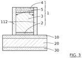
- a grid stack or grid pattern 1 resting on a substrate 100 is provided.
- the substrate 100 can be an elaborate substrate of the semiconductor-on-insulator type, for example a silicon-on-insulator SOI substrate (acronym for “silicon on insulator) or a germanium substrate on GeOI insulator (acronym of English “germanium on insulator) or a silicon-germanium (SiGe) substrate on insulator.
- SOI substrate an elaborate substrate of the semiconductor-on-insulator type
- germanium substrate on GeOI insulator acronym of English “germanium on insulator”
- SiGe silicon-germanium
- This substrate 100 may typically comprise a solid support 30 in silicon, a buried oxide layer 20 also called BOX (“Burried OXide”) and an active semiconductor layer 10 based on silicon or germanium.
- a solid support 30 in silicon a buried oxide layer 20 also called BOX (“Burried OXide”) and an active semiconductor layer 10 based on silicon or germanium.
- BOX Bound OXide
- the active layer 10 is preferably made of silicon (Si) or of silicon-germanium (SiGe).
- the grid stack typically has a height of several tens of nanometers to several hundreds of nanometers.
- this stack will be designated grid pattern 1 or HKMG (acronym for “High K Metal Grid”).
- the step referenced 61 on the figure 6 corresponds to the provision of such a stack.
- a first layer 11 of a dielectric material is deposited on the gate pattern 1 and on the active semiconductor layer 10, preferably in a conformal manner. This deposit corresponds to the step referenced 62 on the figure 6 .
- the deposition of the dielectric material is preferably carried out by a first plasma assisted deposition. It may be a deposition of atomic layers assisted by plasma PEALD (acronym for "Plasma Enhanced Atomic Layer Deposition). Alternatively, it may be a chemical vapor deposition assisted by plasma PECVD (acronym for plasma enhanced chemical vapor deposition). These types of deposits make it possible to obtain a layer whose thickness is fine, perfectly controlled and having a conformal profile. Thus, the thickness of the first layer 11 is homogeneous over the entire surface of the substrate and of the grid pattern 1. These types of deposits also make it possible to obtain a dense, stoichiometric material (for example Si 3 N 4 ), uniformly encapsulating the grid pattern 1.
- PEALD atomic layers assisted by plasma PEALD
- PECVD acronym for plasma enhanced chemical vapor deposition
- these types of plasma-assisted deposition make it possible to limit the deposition temperature so as to preserve the grid pattern 1, in particular the HKMG stack.
- This first layer 11 comprises first lateral portions 11L on each of the lateral flanks of the grid pattern 1, first basal portions 11B at the surface and in contact with the active layer 10 on either side of the grid pattern 1, and a first top portion 11S at the top of the grid pattern 1.
- the first side portions 11L extend in planes perpendicular to the basal plane and the first basal portions 11B extend in planes parallel to the basal plane.
- the first layer 11 is deposited directly in contact with the active layer 10. Also preferably, the first layer 11 is deposited directly in contact with the flanks of the grid pattern 1.
- the first layer 11 has a thickness e1 of between 1 nm and 4 nm, preferably between 1 nm and 3 nm and even more preferably between 1 nm and 2 nm.
- a first step of anisotropic modification of the first layer 11 is carried out. This modification corresponds to step 63 of the figure 6 .
- This anisotropic modification 200 is configured to modify the initial dielectric material.
- the anisotropic modification 200 is configured to modify the dielectric material of the first basal portions 11B over their entire thickness e1, and of the first top portion 11S possibly over their entire thickness e1.
- the first basal and top portions 11B, 11S thus become the first modified portions 11M.
- the first side portions 11L are advantageously unmodified at the end of this anisotropic modification step. Indeed, these first lateral portions 11L extend in planes parallel to the preferred direction of implantation.
- the implantation parameters in particular the nature of the species implanted as well as their concentration, are configured so that the modified portions 11M will have an etching speed greater than the unmodified portions 11L during a subsequent etching step, as will be explained in detail later.
- This implantation is carried out so as to modify the structure of the first layer 11 in the implanted zones, without causing spraying of this layer.
- the implantation is carried out in such a way that the implanted ions are distributed uninterruptedly from the surface of the first layer 11 to the interface between this first layer 11 and the layer which is typically underlying it. active layer 10. This distribution does not present any discontinuity. There are therefore no strata where the implanted species are absent within the first layer 11.
- Plasma implantation has the advantage of allowing continuous implantation in a volume extending from the surface of the implanted layer. This continuity of implantation makes it possible to improve the homogeneity of the modification, which then leads to an etching of the layer implanted at a constant etching rate along the entire thickness of the implanted layer. Furthermore, the increase in selectivity conferred by the implantation with respect to the other layers is effective from the start of the etching of the implanted layer. Plasma implantation thus allows significantly improved control of the engraving precision.
- the active layer 10 is not altered by this step of modification by implantation.
- a second layer 12 of a dielectric material is deposited on the first layer 11 and preferably in contact with the first layer 11. This deposit corresponds to the step referenced 64 on the figure 6 . Preferably, this deposit is carried out in a compliant manner.
- the dielectric material of the second layer 12 is preferably the same as that of the first layer 11. According to an alternative embodiment, the dielectric material of the first layer 11, designated first dielectric material, is different from the dielectric material of the second layer. 12, designated second dielectric material.
- This second deposit is preferably assisted by plasma. It is preferably a PEALD or PECVD deposit.
- the first and second conformal deposits are illustrated and described in more detail below, in the section “conformal deposits of the first and second layers”.
- the second layer 12 has a thickness e2.
- e2 is greater than or equal to e1.
- e1 ⁇ 0.5 * e2.
- e2 is between 5 nm and 30 nm, preferably between 8 nm and 15 nm. This makes it possible to thicken the spacer formed on the flanks 5 of the grid pattern 1 so fast.
- This second layer 12 comprises second lateral portions 12L on each of the lateral flanks of the grid pattern 1, in contact with the first lateral portions 11L.
- the second layer 12 also comprises second basal portions 12B at the surface and in contact with the first modified basal portions 11B, on either side of the grid pattern 1.
- the second layer 12 also comprises a second top portion 12S at the top of the grid pattern 1, on the first modified top portion 11S.
- the second lateral portions 12L extend along planes perpendicular to the basal plane and the second basal portions 12B extend along planes parallel to the basal plane.
- a step of anisotropic etching of the second layer 12 is carried out.
- This etching step is referenced 64 on the figure 6 .
- the preferred direction of this anisotropic etching is substantially parallel to the planes in which the sides of the grid pattern 1 extend.
- this anisotropic etching is configured to remove the second basal portions 12B and the second top portion 12S.
- the second lateral portions 12L located on the flanks of the grid pattern 1 are advantageously preserved at the end of this anisotropic etching step or are consumed over a much smaller thickness.
- the anisotropic etching is carried out so as to expose the first modified portions 11 M.
- the anisotropic etching is stopped so as to consume the entire thickness e2 of the second layer 12 of the portions 12B by stopping at the interface between these 12B portions and the 11 M.
- the thickness e1 is not consumed.
- the stopping of this engraving is time controlled. Provision can nevertheless be made for this anisotropic etching to consume part of the thickness e1, as long as the portions 11M continue to form a protective layer which protects the active layer 10 during this anisotropic etching step.
- a single sequence is carried out comprising the step of depositing the second layer 12 and the anisotropic etching of the portions 12S and 12B.
- a plurality of sequences are carried out successively, each comprising these two steps.
- the thickness of the portions 12L covering the flanks of the grid pattern 1 is increased. This makes it possible to obtain, on the flanks of the grid pattern 1, spacers 112 having a significant thickness without having to etch a significant thickness for the portions 12S and 12B. During this etching, it is then possible to use less aggressive and therefore more precise etching conditions.
- the arrow 66 in figure 6 illustrates this optional embodiment consisting in performing several sequences of steps of deposition and anisotropic etching of the second layer 12.
- the first and second deposits, the anisotropic modification and the anisotropic etching are carried out within the same reactor. This avoids any parasitic oxidation of the various layers and portions between each step. Control of CD and layer morphology is optimized. This also makes it possible to simplify the process and reduce costs.
- a step of removing the first modified portions 11M is performed, as illustrated in figure 4E . This step is referenced 67 in figure 6 .
- This removal step is configured to remove the modified dielectric material accessible, i.e. exposed, selectively to the unmodified dielectric material located on the flanks 5 of the gate pattern 1 and to the semiconductor material of the active layer 10
- an etching chemistry is used making it possible to etch the dielectric material selectively modified with the unmodified dielectric material and with the semiconductor material of the active layer 10.
- the parts 111M of modified dielectric material located plumb side portions 12L are not accessible, for example by a wet etching solution. These parts 111M are in fact hidden and therefore protected by the side portions 12L during this removal step.
- this removal step is controlled so as to be interrupted before these parts 111M are attacked laterally, that is to say in a direction parallel to the upper face of the substrate 100.
- the second side portions 12L and the active layer 10 are thus preserved.
- spacers 112 are formed. These spacers 112 include the portions 111M of modified dielectric material which remained in place after the removal step.
- the figure 5 illustrates on the same time scale the succession of the different phases P1, P2, P3, P4 of conformal deposits (P1 and P3), of anisotropic modification (P2), and of anisotropic etching (P4) within the same reactor. These different phases will be detailed below.
- the figure 5 illustrates a phase P1 corresponding to the conformal deposition of the first layer 11, and a subsequent phase P3 corresponding to the conformal deposition of the second layer 12.
- the deposits of the first 11 and second 12 layers typically comprise a plurality of successive cycles intended to form a plurality of superimposed atomic layers.
- the first 11 and second 12 layers are thus formed by superimposing atomic layers of dielectric material. This makes it possible to precisely control the thicknesses of these layers 11, 12.
- each cycle C typically comprises an injection I of a gaseous precursor within the reactor. This precursor is then dissociated using a P plasma. Reactive species are thus formed and then adsorbed on the deposition surfaces.
- This adsorption makes it possible to form an atomic layer of the dielectric material on the deposition surfaces.
- the gaseous precursors and the plasma used depend on the dielectric material to be deposited.
- the number of cycles carried out determines the number of atomic layers deposited and, in fact, the total thickness of the dielectric layer formed.
- a silicon-based precursor combined with a nitrogen-based plasma can be used.
- a nitrogen-based plasma it is possible, for example, to inject N 2 or NH 3 into the reactor.
- a dichlorosilane precursor (DCS) combined with an ammonia plasma can also be used.
- the deposition temperature is typically between 500 ° C and 650 ° C. This range of deposition temperatures makes it possible to improve the quality of the SiN layer obtained.
- a precursor of Di (Sec-ButylAmino) Silane (DSBAS, SiH 3 N ( s Bu) 2 ) type can be preferably used, combined with an ammonia or nitrogen plasma.
- This type of precursor has the advantage of having a single amino group and allows films of very good quality to be obtained, in particular when it is combined with an N2 plasma and the deposition temperature is of the order of 400 ° C.
- this type of deposit has a very good density, a very low contamination and a low wet etch rate (usually designated by the acronym WER from the English word wet-etch rates).
- boron trichloride BCl3 and methane can for example be added to the DCS.
- the substrate and / or the deposition surfaces are not polarized so as to obtain a conformal deposition.
- the bias voltage is zero or very low.
- a deposition cycle C corresponds to the formation of a layer having a thickness of the order of 0.1 ⁇ to 0.2 ⁇ .
- a C deposition cycle corresponds to the formation of a single atomic layer.
- the number of cycles is thus adapted to the desired layer thickness.
- the thickness of the deposits is controlled in situ by ellipsometry, cycle after cycle.
- the anisotropic modification of the first layer 11 is advantageously carried out within the same reactor, after the deposition of the first layer 11 which is 1 nm to 2 nm thick. As mentioned above, this step makes it possible to modify the first basal and top portions 11B, 11S over the entire thickness e1 of the first layer 11.
- this modification does not modify the first side portions 11L located on the sides of the grid pattern 1.
- This anisotropic modification 200 is carried out by implantation of light ions from a plasma.
- an implantation from a plasma has many advantages since it makes it possible to implant very precisely the entire thickness of the first layer 11 which is thin, without however modifying the layer which is there. is underlying, typically the active layer 10.
- a plasma reactor making it possible to carry out a deposition that is typically a uniform. PEALD or PECVD reactor.
- Plasma can be hydrogen (H) based.
- this modification comprises the implantation of ions based on hydrogen (H, H +, H2 +, H3 +, etc.).
- the implanted ions are helium (He) ions or a mixture of helium and hydrogen (H / He) ions.
- ions can originate, for example, from the following gases introduced into the reactor: H2, HBr; NH3.
- the implantation is adjusted so that the concentration of light ions in the first implanted layer 11 is ideally between 10.10 ⁇ 12-10.1012 ions / cm 3 .
- the voltage bias is low enough to prevent damage to the underlying active layer 10.
- this bias voltage is less than 30V.
- the The method described above provides for a low thickness e1 for the first layer 11. It is then possible to use a reduced polarization voltage which makes it possible to perfectly control the depth at which the ions are implanted.
- the claimed method makes it possible to prevent implanted ions from reaching the active layer 10. This active layer 10 is then not altered.
- the bias voltage is greater than 10V, so as to accelerate and direct the ions in a direction normal to the substrate.
- These implantation conditions are for example determined by simulation using simulation tools of the SRIM (stopping and range of ions matter) or TRIM (transport simulation of ions in matter) type.
- phase P2 of implantation of light ions is illustrated on figure 5 , after phase P1 of depositing the first layer 11.
- the anisotropic etching makes it possible to etch the second basal and top portions 12B, 12S over the entire thickness e2.
- the second side portions 12L are preserved during this etching.
- the anisotropic etching is preferably carried out within the same reactor, after the deposition of the second layer 12 8 nm to 15 nm thick.
- This anisotropic etching is carried out by bombardment of ions from a plasma.
- the plasma used for the anisotropic etching step can be capacitively coupled (CCP) or inductively coupled (ICP).
- the plasma can be based on species heavier than hydrogen and preferably heavier than helium.
- the parameters used for this etching can lead to the bombardment of these species on the second layer 12 leading to its removal by sputtering.
- Heavy ions such as argon (Ar) can be used for this purpose.
- These implantation conditions are for example determined by simulation using simulation tools of the SRIM (stopping and range of ions matter) or TRIM (transport simulation of ions in matter) type.
- phase P4 is illustrated on figure 5 , after phase P3 of depositing the second layer 12.
- Phase P3 and phase P4 constitute a sequence, denoted S1 in figure 5 .
- This sequence makes it possible to leave in place a thickness e2 of dielectric layer on the flanks of the gate pattern 1.
- This sequence S1 can be performed only once or a plurality of times.
- the steps of second conformal deposition and anisotropic etching can be repeated X times so as to obtain second lateral portions 12L having the thickness X.e2.
- Dry or wet etching chemistries can be used.
- the step of removing the first modified portions 11M is carried out by selective wet etching with respect to the semiconductor material of the active layer 10 and the unmodified dielectric material of the spacers 112.
- Such an etching Selective wet can be done using a hydrofluoric acid (HF) based solution.
- HF hydrofluoric acid
- the selective etching is obtained using a solution based on hydrofluoric acid (HF).
- HF hydrofluoric acid
- Such a solution is selective with respect to silicon (Si), silicon-germanium (SiGe), and silicon nitride (SiN).
- the etching speed ratio between modified SiN and SiN is of the order of 30.
- the selective removal of the first portions 11M modified vis-à-vis the first and second side portions 11L, 12L unmodified preferably comprises wet etching at base of a solution comprising hydrofluoric acid (HF) diluted to x% by mass, with 0.1 ⁇ x ⁇ 5.
- HF hydrofluoric acid
- this solution also has a pH less than or equal to 1.5, and preferably strictly less than 1.
- a selectivity S 11M: SiO2 ⁇ 33: 1 can be obtained.
- This improved selectivity makes it possible in particular to preserve the hard SiO2 mask 4 at the top of the grid pattern 1.
- the step of selective removal is carried out by dry etching.
- Such a dry etching can be done by plasma based on nitrogen trifluoride (NF3) and / or ammonia (NH3).
- NF3 nitrogen trifluoride
- NH3 ammonia
- the dry etching can comprise a step of converting the first modified 11M portions into solid salts, followed by a step of sublimation of these solid salts.
- This embodiment makes it possible to obtain very good selectivity of the etching of the modified nitride with respect to the unmodified nitride and to the semiconductor material. This selectivity may be greater than that obtained with an HF solution.
- the dry etching consumes the first modified portions 11M of the first dielectric layer 11, preferentially to the first and second unmodified side portions 11L, 12L and to the active layer 10.
- the risk of excessive consumption of semiconductor material on the surface of the active layer 10 is thus reduced, or even eliminated.
- the claimed method provides a solution that is simple to implement and particularly effective in improving the dimensional control of spacers while reducing the risk of feet appearing or recess at the base of the grid pattern.
- the grid pattern 1 is produced prior to the steps of the invention. These figures thus illustrate a process of the “gate first” type.
- the functional grid stack is produced after the steps of the invention.
- a sacrificial pattern is therefore used in place of the grid stack. This sacrificial pattern is then removed, once the spacers have been made.
- This alternative embodiment is a “gate last” type process.
Abstract
Selon un aspect, on prévoit un procédé de formation d'espaceurs sur un motif de grille comprenant :- Un dépôt d'une première couche diélectrique comprenant des portions basales sur la couche active et des portions latérales sur les flancs du motif,- Une modification anisotrope des seules portions basales de cette première couche, de façon à obtenir des portions basales modifiées.- Un dépôt d'une deuxième couche diélectrique sur la première couche, comprenant également des portions basales et latérales,- Une gravure anisotrope des seules portions basales de cette deuxième couche, de façon à éliminer ces portions basales en conservant les portions latérales,- Un retrait des portions basales modifiées en conservant les premières et deuxièmes portions latérales non modifiées, par gravure sélective du matériau diélectrique modifié vis-à-vis du matériau diélectrique non modifié.- Un domaine d'application privilégié concerne la réalisation des transistors FinFET ou FDSOI.According to one aspect, there is provided a method of forming spacers on a grid pattern comprising: - A deposition of a first dielectric layer comprising basal portions on the active layer and lateral portions on the flanks of the pattern, - A modification anisotropic of the only basal portions of this first layer, so as to obtain modified basal portions - A deposit of a second dielectric layer on the first layer, also comprising basal and lateral portions, - An anisotropic etching of the only basal portions of this second layer, so as to eliminate these basal portions while retaining the lateral portions, - Removal of the modified basal portions while retaining the first and second unmodified lateral portions, by selective etching of the modified dielectric material with respect to the dielectric material unmodified - A preferred field of application concerns the production of FinFET or FDSOI transistors.
Description
La présente invention concerne un procédé de réalisation d'espaceurs d'un transistor. Elle trouvera pour application avantageuse la réalisation d'espaceurs sur les flancs d'une grille d'un transistor avec un excellent contrôle dimensionnel et en évitant la formation de résidus ou de défauts sur ou dans la couche active semiconductrice sous-jacente aux éléments précités. Un domaine d'application concerne la réalisation des transistors FinFET ou FDSOI.The present invention relates to a method of making spacers for a transistor. It will find an advantageous application the production of spacers on the sides of a gate of a transistor with excellent dimensional control and avoiding the formation of residues or defects on or in the active semiconductor layer underlying the aforementioned elements. One field of application concerns the production of FinFET or FDSOI transistors.
Les espaceurs d'un transistor couvrent généralement les flancs latéraux de la grille du transistor. Ils prennent appui sur la couche active du transistor au pied de la grille. Les espaceurs permettent de protéger la grille lors de la formation des régions sources et drains du transistor. Ils permettent également d'isoler électriquement la grille vis-à-vis des régions source et drain, et sont en partie destinés à limiter le couplage capacitif parasite entre la grille et ces régions sources et drains.The spacers of a transistor generally cover the side flanks of the gate of the transistor. They are supported on the active layer of the transistor at the foot of the gate. The spacers make it possible to protect the gate during the formation of the source and drain regions of the transistor. They also allow the gate to be electrically isolated from the source and drain regions, and are in part intended to limit the parasitic capacitive coupling between the gate and these source and drain regions.
Un bon contrôle de l'épaisseur de ces espaceurs, et de la morphologie de ces espaceurs au niveau du pied de grille est un facteur clé pour l'amélioration des performances des transistors.Good control of the thickness of these spacers, and of the morphology of these spacers at the level of the gate foot is a key factor for improving the performance of the transistors.
Les espaceurs sont généralement fabriqués en deux étapes:
- une couche de nitrure de silicium est d'abord déposée de façon conforme sur la
grille 3 et la couche active 10, - cette couche de nitrure de silicium est ensuite gravée de façon anisotrope pour éliminer les parties de celle-ci reposant sur la couche active 10 tout en gardant les parties de celle-ci couvrant les flancs latéraux 5 de la
grille 3 et destinées à former desespaceurs 112.
- a layer of silicon nitride is first deposited in a conformal manner on the
gate 3 and theactive layer 10, - this layer of silicon nitride is then etched anisotropically to eliminate the parts of it resting on the
active layer 10 while keeping the parts of the latter covering thelateral flanks 5 of thegrid 3 and intended to formspacers 112.
La gravure anisotrope conduit généralement à l'une ou l'autre des situations suivantes illustrées en
- la couche active 10 est préservée mais les
espaceurs 112 présentent un pied 111 (situation de sous-gravure illustrée à lafigure 1A ), - les
espaceurs 112 présentent un profil vertical mais la couche active 10R est endommagée (situation de sur-gravure illustrée à lafigure 1B ).
- the
active layer 10 is preserved but thespacers 112 have a foot 111 (situation of under-etching illustrated onfigure 1A ), - the
spacers 112 have a vertical profile but theactive layer 10R is damaged (situation of over-etching illustrated onfigure 1B ).
Avec la réduction des dimensions des transistors et l'apparition de nouvelles architectures de transistors, notamment de transistors nécessitant la formation d'espaceurs au-dessus d'une couche active de faibles épaisseurs, ces situations de sous-gravure et sur-gravure présentent des inconvénients particulièrement préjudiciables. Ces inconvénients sont particulièrement préjudiciables dans les transistors de type FinFET, acronyme du vocable anglais Fin Field-Effect Transistor (signifiant transistor à effet de champ présentant une structure à nageoire), et dans les transistors de type FDSOI, acronyme du vocable anglais Fully Depleted Semiconductor on Insulator (signifiant semi-conducteur sur isolant totalement déserté).With the reduction in the dimensions of transistors and the appearance of new transistor architectures, in particular transistors requiring the formation of spacers above an active layer of small thicknesses, these situations of under-etching and over-etching present particularly damaging disadvantages. These drawbacks are particularly detrimental in transistors of FinFET type, acronym for the English term Fin Field-Effect Transistor (meaning field-effect transistor having a fin structure), and in transistors of the FDSOI type, acronym of the English term Fully Depleted Semiconductor. on Insulator (meaning semi-conductor on insulator completely deserted).
En cas de sous-gravure (
En cas de sur-gravure (
Plusieurs solutions ont été proposées pour réduire les risques d'apparition de pieds ou d'endommagement de la couche sous-jacente.Several solutions have been proposed to reduce the risk of the appearance of feet or of damage to the underlying layer.
Certaines solutions reposent sur l'amélioration des équipements de gravure de la couche de nitrure. Certaines de ces solutions se basent sur l'utilisation de gravures plasma au cours desquelles la température des électrons est réduite pour abaisser l'énergie des ions. Ces solutions présentent néanmoins pour inconvénient de réduire l'anisotropie de la gravure ce qui entraîne une dégradation du contrôle dimensionnel. Par ailleurs ces techniques ne sont pas compatibles avec les chimies polymérisantes puisque l'utilisation de plasmas à faibles énergies entraîne le dépôt de films minces sur les surfaces traitées. Par exemple l'utilisation de chimies, typiquement à base de CF4/CH4 permettent d'améliorer la sélectivité de la gravure du Si3N4 vis-à-vis du Si mais conduit à la formation de pieds importants.Some solutions are based on improving the equipment for etching the nitride layer. Some of these solutions are based on the use of plasma etchings in which the temperature of the electrons is reduced to lower the energy of the ions. These solutions nevertheless have the drawback of reducing the anisotropy of the etching, which leads to a degradation of the dimensional control. Moreover, these techniques are not compatible with polymerizing chemistries since the use of low energy plasmas results in the deposition of thin films on the treated surfaces. For example, the use of chemistries, typically based on CF 4 / CH 4, make it possible to improve the selectivity of the etching of Si 3 N 4 with respect to Si but leads to the formation of large feet.
Un autre type de solutions pour limiter l'apparition du recess et du pied d'espaceur est divulguée dans les documents
Cette solution consiste à remplacer l'étape de gravure anisotrope par une étape d'implantation destinée à modifier les parties de la couche de nitrure de silicium à éliminer, suivie d'une étape de gravure sélective permettant d'éliminer seulement ces parties modifiées de la couche de nitrure de silicium.This solution consists in replacing the anisotropic etching step by an implantation step intended to modify the parts of the silicon nitride layer to be removed, followed by a selective etching step making it possible to remove only these modified parts of the layer. layer of silicon nitride.
Ce procédé de formation d'espaceurs est illustré aux
- une
couche 11 de nitrure de silicium est d'abord déposée de façon conforme sur lagrille 3 et la couche active 10 (figure 2A ), - cette
couche 11 de nitrure de silicium (SiN) est ensuite modifiée localement par implantation anisotrope 200 d'ions légers (H2, He) au niveau desparties 11M de la couche à éliminer (figure 2B ), typiquement sur une épaisseur supérieure à 5 nm, - ces parties modifiées 11M sont ensuite éliminées par gravure sélective du SiN modifié vis-à-vis du SiN non modifié (
figure 2C ).
- a
layer 11 of silicon nitride is first deposited in a conformal manner on thegate 3 and the active layer 10 (figure 2A ), - this
layer 11 of silicon nitride (SiN) is then locally modified byanisotropic implantation 200 of light ions (H2, He) at theparts 11M of the layer to be eliminated (figure 2B ), typically over a thickness greater than 5 nm, - these modified
parts 11M are then removed by selective etching of the modified SiN with respect to the unmodified SiN (figure 2C ).
Cette solution améliore la formation des espaceurs 112 en évitant la formation de pieds d'espaceurs tout en limitant l'apparition de recess, comparativement à une gravure anisotrope classique basée sur une chimie fluorocarbonnée.This solution improves the formation of the
Cependant, il s'avère en pratique que cette solution ne permet pas d'éviter totalement l'apparition du recess.However, it turns out in practice that this solution does not completely prevent the occurrence of recess.
La présente invention vise à pallier certains des inconvénients mentionnés ci-dessus.The present invention aims to overcome some of the drawbacks mentioned above.
Il existe donc un besoin consistant à proposer une solution pour réduire, voire pour éliminer, au moins certains des inconvénients des solutions mentionnées ci-dessus. En particulier, il existe un besoin de formation d'espaceurs 112 présentant une épaisseur très bien contrôlée, sans pieds, et sans impact sur la couche active sous-jacente. Ce besoin est illustré à la
La présente invention a notamment pour objet un procédé de formation d'espaceurs supprimant ou limitant l'apparition de recess dans la couche active, et supprimant ou limitant la formation de pieds au bas des flancs d'un motif de grille d'un transistor.The present invention relates in particular to a method of forming spacers eliminating or limiting the appearance of recess in the active layer, and eliminating or limiting the formation of feet at the bottom of the flanks of a gate pattern of a transistor.
Les autres objets, caractéristiques et avantages de la présente invention apparaîtront à l'examen de la description suivante et des dessins d'accompagnement. Il est entendu que d'autres avantages peuvent être incorporés.The other objects, features and advantages of the present invention will become apparent on examination of the following description and the accompanying drawings. It is understood that other advantages can be incorporated.
Pour atteindre les objectifs mentionnés ci-dessus, la présente invention prévoit selon un premier aspect un procédé de formation d'espaceurs sur un motif de grille de transistor comprenant les étapes successives suivantes :
- Fournir un empilement comprenant au moins une couche active s'étendant selon un plan basal et le motif de grille surmontant la couche active, le motif de grille présentant des flancs latéraux s'étendant selon des plans sensiblement perpendiculaires à la couche active,
- Déposer sur le motif de grille et la couche active une première couche en un premier matériau diélectrique présentant une épaisseur e1. La première couche comprend des premières portions latérales recouvrant les flancs latéraux du motif de grille. La première couche comprend également des premières portions basales, s'étendant parallèlement audit plan basal et recouvrant la couche active, les premières portions latérales étant sensiblement normales aux premières portions basales,
- Réaliser une modification anisotrope de ladite première couche selon une direction privilégiée parallèle aux flancs latéraux, de façon à obtenir des premières portions basales modifiées en conservant des premières portions latérales non modifiées,
- Effectuer au moins une séquence comprenant les étapes suivantes :
- ▪ Déposer sur ladite première couche une deuxième couche en un deuxième matériau diélectrique présentant une épaisseur e2 et comprenant des deuxièmes portions latérales recouvrant les premières portions latérales non modifiées, lesdites deuxièmes portions latérales étant directement au contact des premières portions latérales non modifiées, et des deuxièmes portions basales, s'étendant parallèlement au plan basal et recouvrant les premières portions basales modifiées,
- ▪ Réaliser une gravure anisotrope de ladite deuxième couche selon une direction privilégiée parallèle aux flancs latéraux, de façon à éliminer les deuxièmes portions basales en conservant une partie au moins des deuxièmes portions latérales non modifiées et en conservant une partie au moins de l'épaisseur e1 des premières portions basales modifiées,
- Retirer les premières portions basales modifiées qui sont mises à nu à l'issue de ladite gravure anisotrope de ladite deuxième couche en conservant les premières et deuxièmes portions latérales non modifiées pour former des espaceurs.
- Provide a stack comprising at least one active layer extending along a basal plane and the grid pattern surmounting the active layer, the grid pattern having lateral flanks extending in planes substantially perpendicular to the active layer,
- Depositing on the gate pattern and the active layer a first layer made of a first dielectric material having a thickness e1. The first layer comprises first side portions covering the side flanks of the grid pattern. The first layer also comprises first basal portions, extending parallel to said basal plane and covering the active layer, the first lateral portions being substantially normal to the first basal portions,
- Carry out an anisotropic modification of said first layer in a preferred direction parallel to the lateral flanks, so as to obtain modified first basal portions while retaining unmodified first lateral portions,
- Perform at least one sequence comprising the following steps:
- ▪ Depositing on said first layer a second layer made of a second dielectric material having a thickness e2 and comprising second side portions covering the first unmodified side portions, said second side portions being directly in contact with the first unmodified side portions, and the second basal portions, extending parallel to the basal plane and covering the first modified basal portions,
- ▪ Carry out an anisotropic etching of said second layer in a preferred direction parallel to the lateral flanks, so as to eliminate the second basal portions while retaining at least part of the second unmodified side portions and retaining at least part of the thickness e1 first modified basal portions,
- Remove the first modified basal portions which are exposed at the end of said anisotropic etching of said second layer while keeping the first and second lateral portions unmodified to form spacers.
La présente invention fournit ainsi une solution permettant de former des espaceurs à base des premières et deuxièmes portions latérales non modifiées, présentant une épaisseur E = e1 + e2 sur les flancs latéraux du motif de grille. E se mesure à partir d'un flanc de la grille selon une direction parallèle au plan basal.The present invention thus provides a solution making it possible to form spacers based on the first and second unmodified lateral portions, having a thickness E = e1 + e2 on the lateral flanks of the grid pattern. E is measured from a side of the grid in a direction parallel to the basal plane.
Cette épaisseur E est parfaitement contrôlée et constante le long des flancs latéraux. Avantageusement, les premières et deuxièmes portions latérales non modifiées soient conservées pour former les espaceurs. Cela améliore la précision sur le contrôle de l'épaisseur E et du CD. La formation des espaceurs se fait donc à partir d'au moins deux couches (les première et deuxième couches). Ainsi, selon cet exemple, les première et deuxième couches forment des espaceurs fonctionnels.This thickness E is perfectly controlled and constant along the side flanks. Advantageously, the first and second unmodified side portions are kept to form the spacers. This improves the accuracy on controlling E and CD thickness. The formation of the spacers therefore takes place from at least two layers (the first and second layers). Thus, according to this example, the first and second layers form functional spacers.
Les étapes de gravure anisotrope et de retrait sélectif permettent en outre d'éviter la formation de pieds d'espaceurs à la base du motif de grille.The steps of anisotropic etching and selective removal also make it possible to avoid the formation of feet of spacers at the base of the grid pattern.
La précision et l'uniformité du CD sont ainsi améliorées.The precision and uniformity of the CD are thus improved.
A l'issue du dépôt de la deuxième couche, une couche diélectrique d'épaisseur E comprenant les première et deuxième couches est formée.At the end of the deposition of the second layer, a dielectric layer of thickness E comprising the first and second layers is formed.
Les portions basales de cette couche diélectrique (formées par les premières et deuxièmes portions basales) sont éliminées en deux étapes successives. Cela permet avantageusement de préserver la couche active.The basal portions of this dielectric layer (formed by the first and second basal portions) are removed in two successive steps. This advantageously makes it possible to preserve the active layer.
La gravure anisotrope permet de retirer d'abord les deuxièmes portions basales sur une épaisseur de l'ordre de e2. Cette gravure anisotrope peut éventuellement impacter les premières portions basales sous-jacentes. En revanche, les premières portions basales d'épaisseur e1 permettent ainsi de protéger la couche active sous-jacente de cette gravure anisotrope, qui est une des causes de l'apparition du recess et/ou des défauts structuraux dans la couche active.The anisotropic etching makes it possible to first remove the second basal portions over a thickness of the order of e2. This anisotropic etching can possibly impact the first underlying basal portions. On the other hand, the first basal portions of thickness e1 thus make it possible to protect the underlying active layer from this anisotropic etching, which is one of the causes of the appearance of recess and / or structural defects in the active layer.
Les développements menés dans le cadre de la présente invention ont en effet permis d'identifier que :
- L'endommagement de la couche active est lié à une profondeur de gravure ou d'implantation trop importante.
- L'incertitude sur cette profondeur est d'autant plus grande que la couche diélectrique à implanter ou à graver est épaisse.
- The damage to the active layer is linked to too great an etching or implantation depth.
- The uncertainty over this depth is all the greater the thicker the dielectric layer to be implanted or etched.
Ainsi les solutions connues basées sur la gravure anisotrope de la couche diélectrique d'épaisseur E conduisent à l'apparition d'un recess.Thus the known solutions based on the anisotropic etching of the dielectric layer of thickness E lead to the appearance of a recess.
Les solutions connues basées sur une modification de la couche diélectrique par implantation d'ions hydrogène ou hélium sur toute son épaisseur E conduisent également à l'apparition d'un léger recess. Dans le cadre du développement de la présente invention, il a été identifié que cela est majoritairement dû à une énergie d'implantation importante qui augmente l'incertitude sur la profondeur d'implantation.The known solutions based on a modification of the dielectric layer by implantation of hydrogen or helium ions over its entire thickness E also lead to the appearance of a slight recess. In the context of the development of the present invention, it has been identified that this is mainly due to a high implantation energy which increases the uncertainty on the implantation depth.
Au contraire, selon l'invention, seule l'épaisseur e1 est modifiée par implantation. Cette épaisseur e1 est strictement inférieure à l'épaisseur E de la couche diélectrique. L'énergie d'implantation peut ainsi être réduite par rapport à l'énergie d'implantation utilisée dans les solutions existantes.On the contrary, according to the invention, only the thickness e1 is modified by implantation. This thickness e1 is strictly less than the thickness E of the dielectric layer. The implantation energy can thus be reduced compared to the implantation energy used in existing solutions.
L'incertitude sur la profondeur d'implantation est donc également réduite.The uncertainty on the implantation depth is therefore also reduced.
Il est ainsi possible d'implanter les premières portions basales d'épaisseur e1 sans impacter la couche active sous-jacente.It is thus possible to implant the first basal portions of thickness e1 without impacting the underlying active layer.
L'épaisseur e1 est de préférence faible, par exemple inférieure ou égale à 4 nm, et l'énergie d'implantation est de préférence limitée, par exemple inférieure à 30 eV, de préférence inférieure à 20 eV.The thickness e1 is preferably low, for example less than or equal to 4 nm, and the implantation energy is preferably limited, for example less than 30 eV, preferably less than 20 eV.
Par ailleurs, une modification par implantation de la première couche avant le dépôt de la deuxième couche permet d'éviter un cumul des incertitudes de profondeurs de gravure et d'implantation.Moreover, a modification by implantation of the first layer before the deposition of the second layer makes it possible to avoid an accumulation of uncertainties of etching and implantation depths.
L'incertitude sur la profondeur d'implantation de la première couche d'épaisseur e1 est ainsi minimisée.The uncertainty on the implantation depth of the first layer of thickness e1 is thus minimized.
Le procédé selon l'invention permet avantageusement de former des espaceurs sans pieds, avec un très bon contrôle de CD, et sans endommager la couche active sous-jacente. Un exemple de CD est référencé en
Une solution alternative, qui diffère de la solution revendiquée mais qui aurait pu être envisagée dans le cadre du développement de la présente invention aurait consisté à :
- déposer une couche conforme de SiN dont l'épaisseur est suffisante pour former sur les flancs de la grille des espaceurs,
- graver d'abord partiellement des portions de la couche de SiN en dehors des flancs de façon à réduire leur épaisseur pour obtenir des portions résiduelles d'épaisseur environ égale à e1, puis à
- modifier ces portions résiduelles d'épaisseur e1, pour finalement les retirer de façon sélective.
- deposit a conformal layer of SiN whose thickness is sufficient to form spacers on the sides of the grid,
- first partially etching portions of the SiN layer outside the flanks so as to reduce their thickness to obtain residual portions of thickness approximately equal to e1, then to
- modify these residual portions of thickness e1, in order to finally remove them selectively.
Cette solution alternative n'a pas été retenue dans le cadre de la présente invention car il a été identifié que les portions résiduelles obtenues à l'issue de la gravure ne présentent pas une épaisseur constante et/ou homogène. Cette inhomogénéité d'épaisseur empêche le retrait complet de cette couche sans pour autant altérer la couche sous-jacente lors de la modification par implantation à travers cette couche d'épaisseur inhomogène. Cela conduit à l'apparition de recess après retrait sélectif des portions résiduelles modifiées.This alternative solution was not adopted in the context of the present invention because it was identified that the residual portions obtained at the end of the etching do not have a constant and / or homogeneous thickness. This inhomogeneity of thickness prevents the complete removal of this layer without thereby altering the underlying layer during the modification by implantation through this layer of inhomogeneous thickness. This leads to the appearance of recess after selective removal of the modified residual portions.
La présente invention permet d'éviter ces inconvénients.The present invention makes it possible to avoid these drawbacks.
Les buts, objets, ainsi que les caractéristiques et avantages de l'invention ressortiront mieux de la description détaillée de modes de réalisation de cette dernière qui sont illustrés par les dessins d'accompagnement suivants dans lesquels :
- La
FIGURE 1A illustre schématiquement en coupe un motif de grille flanqué d'espaceurs sur une couche active, les espaceurs présentant un pied selon l'art antérieur. - La
FIGURE 1B illustre schématiquement en coupe un motif de grille flanqué d'espaceurs sur une couche active, la couche active présentant un recess selon l'art antérieur. - Les
FIGURES 2A à 2C illustrent schématiquement des étapes d'un procédé de formation d'espaceurs selon l'art antérieur. - La
FIGURE 2A illustre schématiquement une étape de dépôt d'une couche diélectrique sur un motif de grille selon ce procédé connu de formation d'espaceurs. - La
FIGURE 2B illustre schématiquement une étape de modification de la couche diélectrique par implantation anisotrope selon ce procédé connu de formation d'espaceurs. - La
FIGURE 2C illustre schématiquement une étape de retrait de la couche diélectrique modifiée selon ce procédé connu de formation d'espaceurs. - La
FIGURE 3 illustre schématiquement un motif de grille flanqué d'espaceurs idéal répondant aux besoins des transistors actuels. - Les
FIGURES 4A à 4E illustrent schématiquement des étapes d'un procédé de formation d'espaceurs selon un mode de réalisation de la présente invention. - La
FIGURE 4A illustre schématiquement une étape de dépôt d'une première couche diélectrique sur un motif de grille selon un mode de réalisation de la présente invention. - La
FIGURE 4B illustre schématiquement une étape de modification des portions basales de la première couche diélectrique par implantation anisotrope selon un mode de réalisation de la présente invention. - La
FIGURE 4C illustre schématiquement une étape de dépôt d'une deuxième couche diélectrique sur la première couche diélectrique selon un mode de réalisation de la présente invention. - La
FIGURE 4D illustre schématiquement une étape de gravure anisotrope des portions basales de la deuxième couche diélectrique selon un mode de réalisation de la présente invention. - La
FIGURE 4E illustre schématiquement une étape de retrait des portions basales modifiées de la première couche diélectrique selon un mode de réalisation de la présente invention. - La
FIGURE 5 illustre schématiquement la succession dans le temps des différentes phases de dépôts, d'implantation et de gravure du procédé de formation d'espaceurs selon un mode de réalisation de la présente invention. - La
FIGURE 6 résume certaines étapes du mode de réalisation illustré enfigures 4A à 4E .
- The
FIGURE 1A schematically illustrates in section a grid pattern flanked by spacers on an active layer, the spacers having a foot according to the prior art. - The
FIGURE 1B schematically illustrates in section a grid pattern flanked by spacers on an active layer, the active layer having a recess according to the prior art. - The
FIGURES 2A to 2C schematically illustrate steps of a process for forming spacers according to the prior art. - The
FIGURE 2A schematically illustrates a step of depositing a dielectric layer on a gate pattern according to this known method of forming spacers. - The
FIGURE 2B schematically illustrates a step of modifying the dielectric layer by anisotropic implantation according to this known method of forming spacers. - The
FIGURE 2C schematically illustrates a step of removing the dielectric layer modified according to this known method of forming spacers. - The
FIGURE 3 schematically illustrates a grid pattern flanked by ideal spacers meeting the needs of current transistors. - The
FIGURES 4A to 4E schematically illustrate steps of a method of forming spacers according to an embodiment of the present invention. - The
FIGURE 4A schematically illustrates a step of depositing a first dielectric layer on a gate pattern according to an embodiment of the present invention. - The
FIGURE 4B schematically illustrates a step of modifying the basal portions of the first dielectric layer by anisotropic implantation according to an embodiment of the present invention. - The
FIGURE 4C schematically illustrates a step of depositing a second dielectric layer on the first dielectric layer according to an embodiment of the present invention. - The
FIGURE 4D schematically illustrates a step of anisotropic etching of the basal portions of the second dielectric layer according to an embodiment of the present invention. - The
FIGURE 4E schematically illustrates a step of removing the modified basal portions of the first dielectric layer according to an embodiment of the present invention. - The
FIGURE 5 schematically illustrates the succession over time of the various phases of deposition, implantation and etching of the process for forming spacers according to one embodiment of the present invention. - The
FIGURE 6 summarizes certain steps of the embodiment illustrated infigures 4A to 4E .
Les dessins sont donnés à titre d'exemples et ne sont pas limitatifs de l'invention. Ils constituent des représentations schématiques de principe destinées à faciliter la compréhension de l'invention et ne sont pas nécessairement à l'échelle des applications pratiques. En particulier les dimensions des différentes couches et structures (espaceurs, motif de grille) ne sont pas représentatives de la réalité. Par souci de clarté des illustrations, l'épaisseur de la première couche est représentée de manière exagérément importante relativement à l'épaisseur de la deuxième couche.The drawings are given by way of example and do not limit the invention. They constitute schematic representations of principle intended to facilitate understanding of the invention and are not necessarily on the scale of practical applications. In particular, the dimensions of the different layers and structures (spacers, grid pattern) are not representative of reality. For the sake of clarity of the illustrations, the thickness of the first layer is shown excessively large relative to the thickness of the second layer.
Avant d'entamer une revue détaillée de modes de réalisation de l'invention, il est rappelé que, de manière facultative, l'invention comprend au moins l'une quelconque des caractéristiques optionnelles suivantes qui peuvent être utilisées en association ou alternativement.Before starting a detailed review of embodiments of the invention, it is recalled that, optionally, the invention comprises at least any one of the following optional features which can be used in combination or alternatively.
Selon un exemple, l'épaisseur e1 est inférieure à 4 nm. Cette épaisseur fine autorise l'utilisation de conditions d'implantation faibles en énergie et qui permettent de contrôler précisément la profondeur d'implantation. On évite ainsi d'implanter la couche sous-jacente tout en s'assurant que toute l'épaisseur e1 est modifiée par implantation. Selon un exemple, l'épaisseur e1 est inférieure ou égale à 2 nm (10-9 mètres).According to one example, the thickness e1 is less than 4 nm. This thin thickness allows the use of low energy implantation conditions which allow precise control of the implantation depth. This avoids implanting the underlying layer while ensuring that the entire thickness e1 is modified by implantation. According to one example, the thickness e1 is less than or equal to 2 nm (10 -9 meters).
Selon un exemple, les espaceurs présentent une épaisseur E = e1 + e2 avec E ≤ 30 nm, de préférence E ≤ 15 nm.According to one example, the spacers have a thickness E = e1 + e2 with E ≤ 30 nm, preferably E ≤ 15 nm.
Selon un exemple, les premières portions basales modifiées présentent une épaisseur e1.According to one example, the first modified basal portions have a thickness e1.
Selon un exemple, la modification anisotrope est effectuée en conservant les premières portions latérales non modifiées sur les flancs latéraux du motif de grille.According to one example, the anisotropic modification is carried out while keeping the first unmodified side portions on the side flanks of the grid pattern.
Selon un exemple, lors de l'étape de retrait des premières portions basales modifiées, on retire toutes les premières portions basales modifiées accessibles, en particulier toutes les portions premières portions basales modifiées accessibles à une solution de gravure humide. Les parties des premières portions basales modifiées qui sont surmontées par les deuxièmes portions latérales ne sont pas accessibles. En effet les deuxièmes portions latérales masquent et protègent ces parties des premières portions basales modifiées.According to one example, during the step of removing the first modified basal portions, all the first accessible modified basal portions are removed, in particular all the first modified basal portions accessible to a wet etching solution. The parts of the first modified basal portions which are surmounted by the second lateral portions are not accessible. In fact, the second lateral portions mask and protect these parts from the first modified basal portions.
Selon un exemple, l'étape consistant à retirer les premières portions basales modifiées en conservant les premières et deuxièmes portions latérales non modifiées pour former des espaceurs est effectuée par une gravure sélective du premier matériau diélectrique modifié vis-à-vis du premier matériau diélectrique non modifié, du deuxième matériau diélectrique et du matériau de la couche activeAccording to one example, the step of removing the first modified basal portions while retaining the first and second unmodified lateral portions to form spacers is performed by selective etching of the first modified dielectric material with respect to the first non-modified dielectric material. modified, second dielectric material and active layer material
Selon un exemple, la séquence d'étapes de dépôt et gravure anisotrope de la deuxième couche est réitérée au moins deux fois. Cette réitération de la séquence permet de contrôler avec une très bonne précision l'épaisseur déposée sur les flancs du motif de grille, tout en conservant la première couche qui fait office de protection pour la couche active sous-jacente.According to one example, the sequence of steps of deposition and anisotropic etching of the second layer is reiterated at least twice. This reiteration of the sequence makes it possible to control with very good precision the thickness deposited on the flanks of the grid pattern, while retaining the first layer which acts as protection for the underlying active layer.
Selon un exemple, ladite séquence est réitérée un nombre de fois permettant d'obtenir des espaceurs présentant une épaisseur E = e1 + e2 avec E ≤ 30 nm, de préférence E ≤ 15 nm. On peut ainsi obtenir des espaceurs relativement épais sur les flancs du motif de grille.According to one example, said sequence is reiterated a number of times making it possible to obtain spacers having a thickness E = e1 + e2 with E ≤ 30 nm, preferably E ≤ 15 nm. It is thus possible to obtain relatively thick spacers on the sides of the grid pattern.
Selon un exemple, l'épaisseur e2 déposée au terme de chacune desdites séquences est comprise entre 2 et 5 nanomètres.According to one example, the thickness e2 deposited at the end of each of said sequences is between 2 and 5 nanometers.
Selon un exemple, le dépôt de la première et/ou de la deuxième couches est un dépôt conforme, de sorte que les premières portions latérales et basales présentent sensiblement la même épaisseur e1, et/ou que les deuxièmes portions latérales et basales présentent sensiblement la même épaisseur e2.According to one example, the deposit of the first and / or the second layer is a conformal deposit, so that the first lateral and basal portions have substantially the same thickness e1, and / or that the second lateral and basal portions have substantially the same thickness. same thickness e2.
Selon un exemple, le dépôt des première et deuxième couches se fait par un procédé de dépôt assisté par plasma. Il peut s'agir d'un dépôt de couches atomiques assisté par plasma PEALD (acronyme de « Plasma Enhanced Atomic Layer Déposition). Alternativement, il peut s'agir d'un dépôt en phase vapeur et chimique assisté par plasma PECVD (acronyme de plasma enhanced chemical vapor déposition). Ces procédés permettent de déposer avec précision des couches conformes d'épaisseur très faible.According to one example, the deposition of the first and second layers is done by a plasma assisted deposition process. It can be a deposit of layers atomic assisted plasma PEALD (acronym for "Plasma Enhanced Atomic Layer Deposition). Alternatively, it may be a vapor and chemical deposition assisted by plasma PECVD (acronym for plasma enhanced chemical vapor deposition). These processes make it possible to deposit conforming layers of very low thickness with precision.
Selon un exemple, la modification anisotrope se fait par implantation d'ions provenant d'un plasma selon une direction privilégiée parallèle aux flancs latéraux. Selon un exemple, les ions sont à base d'hydrogène ou d'hélium. Ce type d'implantation permet de modifier la couche implantée sans pour autant la pulvériser.According to one example, the anisotropic modification is carried out by implantation of ions originating from a plasma in a preferred direction parallel to the lateral flanks. According to one example, the ions are based on hydrogen or helium. This type of implantation makes it possible to modify the implanted layer without however spraying it.
Selon un exemple, l'implantation est effectuée en utilisant une tension de polarisation inférieure à 30 V et une pression inférieure à 80 milli Torr.According to one example, the implantation is carried out using a bias voltage lower than 30 V and a pressure lower than 80 milli Torr.
Selon un exemple, la gravure anisotrope de la deuxième couche se fait par des ions provenant d'un plasma selon une direction privilégiée parallèle aux flancs latéraux, à partir d'au moins une espèce plus lourde que l'hélium et de préférence à partir d'argon (Ar).According to one example, the anisotropic etching of the second layer is carried out by ions originating from a plasma in a preferred direction parallel to the lateral flanks, from at least one species heavier than helium and preferably from 'argon (Ar).
Selon un exemple, l'au moins une espèce n'est pas du type CxHy où x est la proportion de carbone (C) et y est la proportion d'hydrogène (H). Ainsi, selon cet exemple, la première couche n'est pas recouverte par un film carboné. Plus précisément, les premières portions latérales 11L ne sont pas au contact d'un film carboné.According to one example, the at least one species is not of the C x H y type where x is the proportion of carbon (C) and y is the proportion of hydrogen (H). Thus, according to this example, the first layer is not covered by a carbon film. More precisely, the first side portions 11L are not in contact with a carbon film.
Selon un exemple, la gravure selon la direction normale au plan basal se fait pour une tension de polarisation inférieure à 30 V et pour une pression inférieure à 80 milli Torr, de préférence inférieure à 10 milli Torr.According to one example, the etching in the direction normal to the basal plane is carried out for a bias voltage of less than 30 V and for a pressure of less than 80 milli Torr, preferably less than 10 milli Torr.
Selon un exemple, le ou les matériaux diélectriques sont choisis parmi le SiN, le SiCO, le SiC, le SiCN, le SiOCN, le SiCBN, le SiOCH, et le SiO2.According to one example, the dielectric material (s) are chosen from SiN, SiCO, SiC, SiCN, SiOCN, SiCBN, SiOCH, and SiO2.
Selon un exemple, le ou les matériaux diélectriques présentent une constante diélectrique inférieure ou égale à 7.According to one example, the dielectric material or materials exhibit a dielectric constant less than or equal to 7.
Selon un exemple, le premier matériau diélectrique et le deuxième matériau diélectrique sont identiques. Cela permet d'obtenir des espaceurs homogène sur les flancs du motif de grille.According to one example, the first dielectric material and the second dielectric material are identical. This makes it possible to obtain homogeneous spacers on the flanks of the grid pattern.
Selon un exemple, le dépôt des première et deuxième couches et la modification anisotrope sont effectuées au sein d'un même réacteur. Cela permet d'éviter les oxydations involontaires, de réduire le nombre d'étapes et la complexité du procédé. Le coût de fabrication s'en trouve également amoindri.According to one example, the deposition of the first and second layers and the anisotropic modification are carried out within the same reactor. This makes it possible to avoid unintentional oxidation, to reduce the number of steps and the complexity of the process. The manufacturing cost is also reduced.
Selon un exemple, la gravure sélective du premier matériau diélectrique modifié est une gravure humide à l'aide d'une solution à base d'acide fluorhydrique (HF).According to one example, the selective etching of the first modified dielectric material is wet etching using a solution based on hydrofluoric acid (HF).
Selon un exemple, la solution à base d'acide fluorhydrique (HF) présente une dilution en HF comprise entre 0.1% et 5% en masse.According to one example, the solution based on hydrofluoric acid (HF) has an HF dilution of between 0.1% and 5% by mass.
Sauf mention explicite, il est précisé que, dans le cadre de la présente invention, la disposition relative d'une troisième couche intercalée entre une première couche et une deuxième couche, ne signifie pas obligatoirement que les couches sont directement au contact les unes des autres, mais signifie que la troisième couche est soit directement au contact des première et deuxième couches, soit séparée de celles-ci par au moins une autre couche ou au moins un autre élément.Unless explicitly stated, it is specified that, in the context of the present invention, the relative arrangement of a third layer interposed between a first layer and a second layer, does not necessarily mean that the layers are directly in contact with each other. , but means that the third layer is either directly in contact with the first and second layers, or separated from them by at least one other layer or at least one other element.
Il est précisé que, dans le cadre de la présente invention, les termes « sur », « surmonte », « recouvre », « sous-jacent », en « vis-à-vis » et leurs équivalents ne signifient pas forcément « au contact de ». Ainsi par exemple, le dépôt, le report, le collage, l'assemblage ou l'application d'une première couche sur une deuxième couche, ne signifie pas obligatoirement que les deux couches sont directement au contact l'une de l'autre, mais signifie que la première couche recouvre au moins partiellement la deuxième couche en étant soit directement à son contact, soit en étant séparée d'elle par au moins une autre couche ou au moins un autre élément.It is specified that, within the framework of the present invention, the terms “on”, “overcomes”, “covers”, “underlying”, in “vis-à-vis” and their equivalents do not necessarily mean “in the face”. contact of ”. Thus, for example, the deposition, the transfer, the bonding, the assembly or the application of a first layer on a second layer, does not necessarily mean that the two layers are directly in contact with one another, but means that the first layer at least partially covers the second layer by being either directly in contact with it, or by being separated from it by at least one other layer or at least one other element.
Une couche peut par ailleurs être composée de plusieurs sous-couches d'un même matériau ou de matériaux différents.A layer can also be made up of several sub-layers of the same material or of different materials.
Les étapes de formation des différentes couches s'entendent au sens large : elles peuvent être réalisées en plusieurs sous-étapes (en particulier cycles de d'adsorption de précurseurs et purge dans le cas d'un dépôt de couches minces atomiques).The stages of formation of the various layers are understood in the broad sense: they can be carried out in several sub-stages (in particular cycles of adsorption of precursors and purging in the case of a deposition of thin atomic layers).
On entend par un substrat, une couche, un dispositif, « à base » d'un matériau M, un substrat, une couche, un dispositif comprenant ce matériau M uniquement ou ce matériau M et éventuellement d'autres matériaux, par exemple des éléments d'alliage, des impuretés ou des éléments dopants. Ainsi, une couche diélectrique à base de nitrure de silicium SiN peut par exemple comprendre du nitrure de silicium non stœchiométrique (SiN), ou du nitrure de silicium stœchiométrique (Si3N4), ou encore un oxy-nitrure de silicium (SiON).By a substrate, a layer, a device, “based” on a material M, is meant a substrate, a layer, a device comprising this material M only or this material M and possibly other materials, for example elements. alloy, impurities or doping elements. Thus, a dielectric layer based on silicon nitride SiN can for example comprise non-stoichiometric silicon nitride (SiN), or stoichiometric silicon nitride (Si 3 N 4 ), or even a silicon oxy-nitride (SiON) .
Le mot « diélectrique » qualifie un matériau dont la conductivité électrique est suffisamment faible dans l'application donnée pour servir d'isolant. Dans la présente invention, un matériau diélectrique présente de préférence une constante diélectrique inférieure à 7.The word "dielectric" qualifies a material whose electrical conductivity is sufficiently low in the given application to serve as an insulator. In the present invention, a dielectric material preferably has a dielectric constant of less than 7.
Les matériaux diélectriques envisagés dans le cadre la présente invention sont, de manière non limitative, le SiN, le SiCO, le SiC, le SiCN, le SiOCN, le SiBCN, le SiOCH, le SiO2.The dielectric materials envisaged in the context of the present invention are, in a nonlimiting manner, SiN, SiCO, SiC, SiCN, SiOCN, SiBCN, SiOCH, SiO2.
Le matériau diélectrique modifié est réputé différent du matériau diélectrique non modifié.The modified dielectric material is deemed to be different from the unmodified dielectric material.
Les termes « matériau diélectrique », « matériau diélectrique initial », « matériau diélectrique non modifié » sont synonymes.The terms “dielectric material”, “initial dielectric material”, “unmodified dielectric material” are synonymous.
Les termes « motif de grille », «empilement de grille », « grille » sont employés en synonymes.The terms "grid pattern", "grid stack", "grid" are used synonymously.
Dans la présente demande de brevet, on parlera préférentiellement d'épaisseur pour une couche et de hauteur pour un dispositif (transistor ou grille par exemple). La hauteur est prise selon une direction normale au plan basal. L'épaisseur en un point de la couche est prise selon une direction normale à la tangente à la couche en ce point. Ainsi, sur les figures, l'épaisseur est prise selon la verticale dans les zones qui s'étendent principalement à l'horizontale, telles que les portions basales. En revanche, l'épaisseur est prise selon l'horizontale dans les zones qui s'étendent principalement à la verticale, telles que les portions latérales. Ainsi, l'épaisseur des espaceurs qui recouvrent des flancs verticaux d'une grille ou d'un motif de grille sera mesurée selon la direction horizontale sur les figures.In the present patent application, we will preferably speak of thickness for a layer and height for a device (transistor or gate for example). The height is taken in a direction normal to the basal plane. The thickness at a point of the layer is taken in a direction normal to the tangent to the layer at this point. Thus, in the figures, the thickness is taken along the vertical in the areas which extend mainly horizontally, such as the basal portions. On the other hand, the thickness is taken along the horizontal in the areas which extend mainly vertically, such as the side portions. Thus, the thickness of the spacers which cover the vertical sides of a grid or of a grid pattern will be measured in the horizontal direction in the figures.
Les termes « sensiblement », « environ », « de l'ordre de » signifient « à 10% près » ou, lorsqu'il s'agit d'une orientation angulaire, « à 10° près ». Ainsi, une direction sensiblement normale à un plan signifie une direction présentant un angle de 90±10° par rapport au plan.The terms “substantially”, “approximately”, “of the order of” mean “within 10%” or, in the case of an angular orientation, “within 10 °”. Thus, a direction substantially normal to a plane means a direction having an angle of 90 ± 10 ° with respect to the plane.
Pour déterminer la géométrie des espaceurs et la disposition des différentes couches, on peut procéder à des analyses de microscopie électronique, en particulier de Microscopie Electronique à Balayage (MEB) ou de Microscopie Electronique en Transmission (MET ou TEM).To determine the geometry of the spacers and the arrangement of the different layers, it is possible to carry out electron microscopy analyzes, in particular Scanning Electron Microscopy (SEM) or Transmission Electron Microscopy (TEM or TEM).
Les compositions chimiques des différentes couches ou régions peuvent être déterminées à l'aide de la méthode bien connue EDX ou X-EDS, acronyme de « energy dispersive x-ray spectroscopy » qui signifie « analyse dispersive en énergie de photons X ».The chemical compositions of the different layers or regions can be determined using the well-known EDX or X-EDS method, acronym for “energy dispersive x-ray spectroscopy” which means “energy dispersive analysis of X photons”.
Cette méthode est bien adaptée pour analyser la composition de couches de faibles épaisseurs telles que la couche active et les espaceurs. Elle peut être mise en œuvre sur des coupes métallurgiques au sein d'un MEB ou d'un MET.This method is well suited for analyzing the composition of thin layers such as the active layer and spacers. It can be implemented on metallurgical sections within a SEM or a TEM.
Ces techniques permettent notamment de déterminer si les espaceurs présentent un pied, s'il y a des résidus de couche diélectrique sur la couche active, s'il y a des défauts structuraux ou du recess dans la couche active.These techniques make it possible in particular to determine whether the spacers have a base, whether there are dielectric layer residues on the active layer, whether there are structural defects or recess in the active layer.
En mettant en œuvre le procédé selon l'invention, des espaceurs sont formés sans pied ou avec un pied de taille réduite, les résidus de couche diélectrique sont réduits voire éliminés, et la couche active est préservée des défauts structuraux ou du recess.By implementing the method according to the invention, spacers are formed without a foot or with a foot of reduced size, the dielectric layer residues are reduced or even eliminated, and the active layer is preserved from structural defects or from recess.
Un mode de réalisation du procédé de formation d'espaceurs selon l'invention va maintenant être décrit en référence aux
Selon ce mode de réalisation, un empilement de grille ou motif de grille 1 reposant sur un substrat 100 est fourni.According to this embodiment, a grid stack or
Le substrat 100 peut être un substrat élaboré de type semi-conducteur sur isolant, par exemple un substrat silicium sur isolant SOI (acronyme de l'anglais « silicon on insulator) ou un substrat germanium sur isolant GeOI (acronyme de l'anglais « germanium on insulator) ou encore un substrat silicium-germanium (SiGe) sur isolant.The
Ce substrat 100 peut typiquement comprendre un support massif 30 en silicium, une couche d'oxyde enterrée 20 également dénommée BOX (« Burried OXide ») et une couche active 10 semiconductrice à base de silicium ou de germanium.This
La couche active 10 est de préférence en silicium (Si) ou en silicium-germanium (SiGe).The
La couche active 10 est surmontée d'un empilement de grille ou motif de grille 1. De manière classique, l'empilement de grille peut comprendre une succession de couches disposées à partir de la couche active 10, telles que, par exemple :
- une couche à haute constante diélectrique 2, dite couche « high k »,
une grille 3 métallique, par exemple en silicium polycristallin,une couche 4 formant un masque dur au sommet de lagrille 3.
- a high dielectric
constant layer 2, called a “high k” layer, - a
metallic grid 3, for example made of polycrystalline silicon, - a
layer 4 forming a hard mask at the top of thegrid 3.
L'empilement de grille présente typiquement une hauteur de plusieurs dizaines de nanomètres à plusieurs centaines de nanomètres.The grid stack typically has a height of several tens of nanometers to several hundreds of nanometers.
Dans la suite de la description, cet empilement sera désigné motif de grille 1 ou HKMG (acronyme de « High K Metal Grid »).In the remainder of the description, this stack will be designated
L'étape référencée 61 sur la
Tel qu'illustré à la
Le dépôt du matériau diélectrique est de préférence effectué par un premier dépôt assisté par plasma. Il peut s'agir d'un dépôt de couches atomiques assisté par plasma PEALD (acronyme de « Plasma Enhanced Atomic Layer Déposition). Alternativement, il peut s'agir d'un dépôt chimique en phase vapeur assisté par plasma PECVD (acronyme de plasma enhanced chemical vapor déposition). Ces types de dépôts permettent d'obtenir une couche dont l'épaisseur est fine, parfaitement contrôlée et présentant un profil conforme. Ainsi, l'épaisseur de la première couche 11 est homogène sur toute la surface du substrat et du motif de grille 1. Ces types de dépôts permettent également d'obtenir un matériau dense, stœchiométrique (par exemple Si3N4), encapsulant uniformément le motif de grille 1.The deposition of the dielectric material is preferably carried out by a first plasma assisted deposition. It may be a deposition of atomic layers assisted by plasma PEALD (acronym for "Plasma Enhanced Atomic Layer Deposition). Alternatively, it may be a chemical vapor deposition assisted by plasma PECVD (acronym for plasma enhanced chemical vapor deposition). These types of deposits make it possible to obtain a layer whose thickness is fine, perfectly controlled and having a conformal profile. Thus, the thickness of the
En outre ces types de dépôts assistés par plasma permettent de limiter la température de dépôt de façon à préserver le motif de grille 1, notamment l'empilement HKMG.In addition, these types of plasma-assisted deposition make it possible to limit the deposition temperature so as to preserve the
Cette première couche 11 comprend des premières portions latérales 11L sur chacun des flancs latéraux du motif de grille 1, des premières portions basales 11B en surface et au contact de la couche active 10 de part et d'autre du motif de grille 1, et une première portion sommitale 11S au sommet du motif de grille 1. Les premières portions latérales 11L s'étendent selon des plans perpendiculaires au plan basal et les premières portions basales 11B s'étendent selon des plans parallèles au plan basal.This
De préférence, la première couche 11 est déposée directement au contact de la couche active 10. De préférence également, la première couche 11 est déposée directement au contact des flancs du motif de grille 1.Preferably, the
La première couche 11 présente une épaisseur e1 comprise entre 1 nm et 4 nm, de préférence entre 1 nm et 3 nm et encore plus préférentiellement entre 1 nm et 2 nm.The
Comme illustré à la
Elle peut notamment être réalisée par implantation d'espèces, en particulier des ions, au niveau des portions de la couche 11 s'étendant principalement selon le plan basal. Cette implantation anisotrope est effectuée selon une direction principale de bombardement des ions. Cette direction principale est donc parallèle aux flancs latéraux du motif de grille 1.It can in particular be carried out by implantation of species, in particular ions, at the portions of the
La modification anisotrope 200 est configurée pour modifier le matériau diélectrique des premières portions basales 11B sur toute leur épaisseur e1, et de la première portion sommitale 11S éventuellement sur toute son épaisseur e1.The
Les premières portions basales et sommitale 11B, 11S deviennent ainsi des premières portions modifiées 11M.The first basal and
Les premières portions latérales 11L sont avantageusement non modifiées à l'issue de cette étape de modification anisotrope. En effet, ces premières portions latérales 11L s'étendent dans des plans parallèles à la direction privilégiée d'implantation.The first side portions 11L are advantageously unmodified at the end of this anisotropic modification step. Indeed, these first lateral portions 11L extend in planes parallel to the preferred direction of implantation.
Les paramètres de l'implantation, en particulier la nature des espèces implantées ainsi que leur concentration, sont configurés de sorte à ce que les portions modifiées 11M présenteront une vitesse de gravure supérieure aux portions non modifiées 11L lors d'une étape de gravure ultérieure, comme cela sera expliqué en détail par la suite.The implantation parameters, in particular the nature of the species implanted as well as their concentration, are configured so that the modified
Comme cela sera décrit par la suite dans la section « modification anisotrope », on privilégie une modification par implantation d'ions légers à partir d'un plasma.As will be described below in the “anisotropic modification” section, a modification by implantation of light ions from a plasma is preferred.
Cette implantation est effectuée de manière à modifier la structure de la première couche 11 dans les zones implantées, sans entraîner de pulvérisation de cette couche. Avantageusement, l'implantation est effectuée de manière à ce que les ions implantés soient répartis de manière ininterrompue depuis la surface de la première couche 11 jusqu'à l'interface entre cette première couche 11 et la couche qui lui est sous-jacente typiquement la couche active 10. Cette répartition ne présente pas de discontinuité. Il n'y a donc pas de strates où les espèces implantées sont absentes au sein de la première couche 11.This implantation is carried out so as to modify the structure of the
Une implantation par plasma a pour avantage de permettre une implantation de manière continue dans un volume s'étendant dès la surface de la couche implantée. Cette continuité d'implantation permet d'améliorer l'homogénéité de la modification, ce qui conduit ensuite à une gravure de la couche implantée à une vitesse de gravure constante le long de toute l'épaisseur de la couche implantée. Par ailleurs, l'augmentation de la sélectivité conférée par l'implantation vis à vis des autres couches est effective dès le début de la gravure de la couche implantée. L'implantation par plasma permet ainsi un contrôle significativement amélioré de la précision de gravure.Plasma implantation has the advantage of allowing continuous implantation in a volume extending from the surface of the implanted layer. This continuity of implantation makes it possible to improve the homogeneity of the modification, which then leads to an etching of the layer implanted at a constant etching rate along the entire thickness of the implanted layer. Furthermore, the increase in selectivity conferred by the implantation with respect to the other layers is effective from the start of the etching of the implanted layer. Plasma implantation thus allows significantly improved control of the engraving precision.
Par ailleurs, de manière particulièrement avantageuse puisque l'épaisseur e1 est faible, il est alors possible d'implanter toute cette épaisseur avec des ions présentant une énergie faible. Dès lors, il est possible de contrôler à la fois que la première couche est effectivement implantée sur toute son épaisseur e1 et à la fois que les ions implantés n'atteignent pas la couche active 10 sous-jacente. Ainsi, contrairement à des solutions existantes qui prévoient l'implantation d'une couche plus épaisse, la couche active 10 n'est pas altérée par cette étape de modification par implantation.Moreover, in a particularly advantageous manner since the thickness e1 is small, it is then possible to implant all this thickness with ions having a low energy. Consequently, it is possible to check both that the first layer is effectively implanted over its entire thickness e1 and at the same time that the implanted ions do not reach the underlying
Comme illustré à la
Ce deuxième dépôt est de préférence assisté par plasma. Il s'agit de préférence d'un dépôt PEALD ou PECVD.This second deposit is preferably assisted by plasma. It is preferably a PEALD or PECVD deposit.
Les premier et deuxième dépôts conformes sont illustrés et décrits plus en détail dans la suite, dans la section « dépôts conformes des première et deuxième couches ».The first and second conformal deposits are illustrated and described in more detail below, in the section “conformal deposits of the first and second layers”.
La deuxième couche 12 présente une épaisseur e2. Avantageusement, e2 est supérieure ou égale à e1. De préférence e1<0,5*e2. De préférence, e2 est comprise entre 5 nm et 30 nm, de préférence entre 8 nm et 15 nm. Cela permet d'épaissir l'espaceur formé sur les flancs 5 du motif de grille 1 de manière rapide. Selon un mode de réalisation alternatif, on peut avoir e2 inférieure ou égale à e1.The
Cette deuxième couche 12 comprend des deuxièmes portions latérales 12L sur chacun des flancs latéraux du motif de grille 1, au contact des premières portions latérales 11L. Ainsi selon cet exemple, il n'y a pas une autre couche, par exemple une couche carbonée, située entre les deuxièmes portions latérales 12L et les premières portions latérales 11L.This
La deuxième couche 12 comprend également des deuxièmes portions basales 12B en surface et au contact des premières portions basales 11B modifiées, de part et d'autre du motif de grille 1.The
La deuxième couche 12 comprend également une deuxième portion sommitale 12S au sommet du motif de grille 1, sur la première portion sommitale 11S modifiée.The
Les deuxièmes portions latérales 12L s'étendent selon des plans perpendiculaires au plan basal et les deuxièmes portions basales 12B s'étendent selon des plans parallèles au plan basal.The second
Comme illustré à la
Différentes solutions de gravure adaptées à cette étape de gravure anisotrope sont détaillées dans la suite, dans la section « gravure anisotrope ».Different etching solutions suitable for this anisotropic etching step are detailed below, in the “anisotropic etching” section.
La gravure anisotrope est effectuée de sorte à exposer les premières portions modifiées 11 M. De préférence, la gravure anisotrope est stoppée de manière à consommer toute l'épaisseur e2 de la deuxième couche 12 des portions 12B en s'arrêtant à l'interface entre ces portions 12B et les portions 11 M. Ainsi, l'épaisseur e1 n'est pas consommée. L'arrêt de cette gravure est contrôlé au temps. On peut néanmoins prévoir que cette gravure anisotrope consomme une partie de l'épaisseur e1, tant que les portions 11M continuent de former une couche de protection qui protège la couche active 10 lors de cette étape de gravure anisotrope.The anisotropic etching is carried out so as to expose the first modified
Ainsi, à l'issue de la gravure anisotrope des portions 12S et 12B de la deuxième couche 12 :
- on conserve tout ou partie de l'épaisseur des
portions 12L de la deuxième couche 12 situées sur les flancs dumotif 1 de grille. On forme ainsi sur cesflancs un espaceur 112. - on fait en sorte de conserver toute l'épaisseur, ou au moins une partie de l'épaisseur des premières portions modifiées 11 M. Ces portions modifiées 11M recouvrent ainsi la couche active 10 et agissent sur cette dernière comme une couche de protection ou de masquage durant la gravure anisotrope de la deuxième couche 12. Grâce à la présence des portions modifiées 11M de la première couche 11, la couche active 10 n'est ainsi pas endommagée lors de la gravure anisotrope des
portions 12S et
- all or part of the thickness of the
portions 12L of thesecond layer 12 located on the sides of thegrid pattern 1 is retained. Aspacer 112 is thus formed on these sides. - care is taken to keep the entire thickness, or at least part of the thickness of the first modified
portions 11 M. These modifiedportions 11M thus cover theactive layer 10 and act on the latter as a protective or masking layer during the anisotropic etching of thesecond layer 12. Thanks to the presence of the modifiedportions 11M of thefirst layer 11, theactive layer 10 is thus not damaged during the anisotropic etching of theportions
Sur l'exemple illustré aux
De façon particulièrement avantageuse, les premier et deuxième dépôts, la modification anisotrope et la gravure anisotrope sont effectués au sein d'un même réacteur. Cela permet d'éviter toute oxydation parasite des différentes couches et portions entre chaque étape. Le contrôle du CD et de la morphologie des couches est optimisé. Cela permet également de simplifier le procédé et de réduire les couts.Particularly advantageously, the first and second deposits, the anisotropic modification and the anisotropic etching are carried out within the same reactor. This avoids any parasitic oxidation of the various layers and portions between each step. Control of CD and layer morphology is optimized. This also makes it possible to simplify the process and reduce costs.
A l'issue de la gravure anisotrope, une étape de retrait des premières portions modifiées 11M est effectuée, tel qu'illustré à la
Cette étape de retrait est configurée pour retirer le matériau diélectrique modifié accessible, c'est-à-dire mis à nu, sélectivement au matériau diélectrique non modifié situé sur les flancs 5 du motif de grille 1 et au matériau semiconducteur de la couche active 10. Pour cela, on utilise une chimie de gravure permettant de graver le matériau diélectrique modifié sélectivement au matériau diélectrique non modifié et au matériau semi-conducteur de la couche active 10. On notera que les parties 111M de matériau diélectrique modifié situées à l'aplomb des portions latérales 12L ne sont pas accessibles, par exemple par une solution de gravure humide. Ces parties 111M sont en effet masquées et donc protégées par les portions latérales 12L lors de cette étape de retrait. Par ailleurs, cette étape de retrait est contrôlée de sorte à être interrompue avant que ces parties 111M ne soient attaquées latéralement, c'est-à-dire selon une direction parallèle à la face supérieure du substrat 100.This removal step is configured to remove the modified dielectric material accessible, i.e. exposed, selectively to the unmodified dielectric material located on the
Les deuxièmes portions latérales 12L et la couche active 10 sont ainsi préservées.The
Différents modes de réalisation de l'étape de retrait sont décrits en détail dans la suite, dans la section « retrait sélectif ».Different embodiments of the removal step are described in detail below, in the section “selective removal”.
A l'issue de cette étape de retrait, les espaceurs 112 sont formés. Ces espaceurs 112 comprennent les parties 111M de matériau diélectrique modifié qui sont restées en place à l'issue de l'étape de retrait.At the end of this removal step, the
Ces espaceurs 112 comprennent les première et deuxième portions latérales 11L, 12L. Ils présentent ainsi une épaisseur E = e1 + e2 uniforme et parfaitement contrôlée.These
Différents modes de réalisation des étapes mentionnées ci-dessus vont maintenant être décrits en détail.Different embodiments of the steps mentioned above will now be described in detail.
La
La
Les dépôts des première 11 et deuxième 12 couches comprennent typiquement une pluralité de cycles successifs destinés à former une pluralité de couches atomiques superposées. Les première 11 et deuxième 12 couches sont ainsi formées par superposition de couches atomiques de matériau diélectrique. Cela permet de contrôler avec précision les épaisseurs de ces couches 11, 12.The deposits of the first 11 and second 12 layers typically comprise a plurality of successive cycles intended to form a plurality of superimposed atomic layers. The first 11 and second 12 layers are thus formed by superimposing atomic layers of dielectric material. This makes it possible to precisely control the thicknesses of these
Tel qu'illustré à la
Cette adsorption permet de former une couche atomique du matériau diélectrique sur les surfaces de dépôt.This adsorption makes it possible to form an atomic layer of the dielectric material on the deposition surfaces.
L'excédent de précurseur et/ou d'espèces réactives est ensuite évacué par une purge V du réacteur en fin de cycle C.The excess precursor and / or reactive species is then removed by a purge V from the reactor at the end of cycle C.
Les précurseurs gazeux et le plasma utilisés dépendent du matériau diélectrique à déposer.The gaseous precursors and the plasma used depend on the dielectric material to be deposited.
Le nombre de cycles réalisés détermine le nombre de couches atomiques déposées et, de fait, l'épaisseur totale de la couche diélectrique formée.The number of cycles carried out determines the number of atomic layers deposited and, in fact, the total thickness of the dielectric layer formed.
Pour former une couche en nitrure de silicium SiN, un précurseur à base de silicium combiné à un plasma à base d'azote peuvent être utilisés. Pour former ce plasma à base d'azote on peut par exemple injecter dans le réacteur du N2 ou du NH3.To form a layer of silicon nitride SiN, a silicon-based precursor combined with a nitrogen-based plasma can be used. To form this nitrogen-based plasma, it is possible, for example, to inject N 2 or NH 3 into the reactor.
Un précurseur dichlorosilane (DCS) combiné à un plasma d'ammoniac peut aussi être utilisé. La température de dépôt est typiquement comprise entre 500 °C et 650 °C. Cette gamme de températures de dépôt permet d'améliorer la qualité de la couche de SiN obtenue.A dichlorosilane precursor (DCS) combined with an ammonia plasma can also be used. The deposition temperature is typically between 500 ° C and 650 ° C. This range of deposition temperatures makes it possible to improve the quality of the SiN layer obtained.
Un précurseur de type Di(Sec-ButylAmino)Silane (DSBAS, SiH3N(sBu)2) peut être préférentiellement utilisé, combiné à un plasma d'ammoniac ou d'azote. Ce type de précurseur a pour avantage d'avoir un seul groupement amino et permet l'obtention de films de très bonne qualité, en particulier lorsqu'il est combiné à un plasma de N2 et que la température de dépôt est de l'ordre de 400°C. En particulier, ce type de dépôts présente une très bonne densité, une très faible contamination et une vitesse de gravure humide faible (habituellement désignée par l'acronyme WER du vocable anglais wet-etch rates).A precursor of Di (Sec-ButylAmino) Silane (DSBAS, SiH 3 N ( s Bu) 2 ) type can be preferably used, combined with an ammonia or nitrogen plasma. This type of precursor has the advantage of having a single amino group and allows films of very good quality to be obtained, in particular when it is combined with an N2 plasma and the deposition temperature is of the order of 400 ° C. In particular, this type of deposit has a very good density, a very low contamination and a low wet etch rate (usually designated by the acronym WER from the English word wet-etch rates).
Pour former une couche en SiBCN, du trichlorure de bore BCl3 et du méthane peuvent par exemple être ajoutés au DCS.To form a SiBCN layer, boron trichloride BCl3 and methane can for example be added to the DCS.
De préférence, le substrat et/ou les surfaces de dépôt ne sont pas polarisés de façon à obtenir un dépôt conforme. Autrement dit, la tension de polarisation est nulle ou très faible.Preferably, the substrate and / or the deposition surfaces are not polarized so as to obtain a conformal deposition. In other words, the bias voltage is zero or very low.
De préférence, un cycle de dépôt C correspond à la formation d'une couche présentant une épaisseur de l'ordre de 0,1Å à 0,2Å. De préférence, un cycle de dépôt C correspond à la formation d'une unique couche atomique.Preferably, a deposition cycle C corresponds to the formation of a layer having a thickness of the order of 0.1Å to 0.2Å. Preferably, a C deposition cycle corresponds to the formation of a single atomic layer.
Par exemple, 80 cycles successifs C1-Cn (n=80) permettent de former une couche diélectrique de 12 nm environ (
Le nombre de cycles est ainsi adapté à l'épaisseur de couche souhaitée.The number of cycles is thus adapted to the desired layer thickness.
Selon une possibilité avantageuse, l'épaisseur des dépôts est contrôlée in situ par ellipsométrie, cycle après cycle.According to an advantageous possibility, the thickness of the deposits is controlled in situ by ellipsometry, cycle after cycle.
La modification anisotrope de la première couche 11 est avantageusement effectuée au sein du même réacteur, après le dépôt de la première couche 11 de 1 nm à 2 nm d'épaisseur. Comme mentionné ci-dessus, cette étape permet de modifier les premières portions basales et sommitale 11B, 11S sur toute l'épaisseur e1 de la première couche 11.The anisotropic modification of the
En revanche, cette modification ne modifie pas les premières portions latérales 11L situées sur les flancs du motif de grille 1.On the other hand, this modification does not modify the first side portions 11L located on the sides of the
Cette modification anisotrope 200 est effectuée par implantation d'ions légers à partir d'un plasma. Comme indiqué ci-dessus, une implantation à partir d'un plasma présente de nombreux avantages puisqu'elle permet d'implanter de manière très précise toute l'épaisseur de la première couche 11 qui est mince, sans pour autant modifier la couche qui lui est sous-jacente, typiquement la couche active 10.This
Si l'on souhaite utiliser le même réacteur de gravure pour l'étape de dépôt de la première couche 11 et pour l'étape de modification anisotrope 200, il est préférable d'utiliser un réacteur plasma permettant d'effectuer un dépôt conforme typiquement un réacteur PEALD ou PECVD.If it is desired to use the same etching reactor for the step of depositing the
Le plasma peut être à base d'hydrogène (H). Selon un exemple de réalisation, cette modification comprend l'implantation d'ions à base d'hydrogène (H, H+, H2+, H3+, etc....). Selon un autre mode de réalisation les ions implantés sont des ions d'hélium (He) ou un mélange d'ions d'hélium et d'hydrogène (H/He).Plasma can be hydrogen (H) based. According to an exemplary embodiment, this modification comprises the implantation of ions based on hydrogen (H, H +, H2 +, H3 +, etc.). According to another embodiment, the implanted ions are helium (He) ions or a mixture of helium and hydrogen (H / He) ions.
Ces ions peuvent provenir par exemple des gaz suivants introduits dans le réacteur : H2, HBr ; NH3.These ions can originate, for example, from the following gases introduced into the reactor: H2, HBr; NH3.
Pour obtenir une bonne sélectivité lors de l'étape de retrait des portions modifiées 11M, on règle l'implantation de sorte à ce que la concentration en ions légers dans la première couche 11 implantée soit idéalement comprise entre 10.10^12-10.1012 ions/cm3.To obtain good selectivity during the step of removing the modified
Afin d'obtenir une implantation précise sur toute l'épaisseur e1, et en particulier pour stopper cette implantation à l'interface entre la première couche 11 diélectrique et la couche active 10, parmi les paramètres retenus pour le plasma, on prévoit que la tension de polarisation (bias) soit suffisamment faible pour éviter un endommagement de la couche active 10 sous-jacente. De préférence cette tension de polarisation est inférieure à 30V. En effet, le procédé décrit ci-dessus prévoit une épaisseur e1 faible pour la première couche 11. Il est alors possible d'utiliser une tension de polarisation réduite qui permet de contrôler parfaitement la profondeur à laquelle les ions sont implantés. Contrairement à des procédés connus visant à modifier des couches d'épaisseurs plus épaisses, typiquement supérieure à 8 nm, le procédé revendiqué permet d'éviter que des ions implantés parviennent jusque dans la couche active 10. Cette couche active 10 n'est alors pas altérée. De préférence, la tension de polarisation est supérieure à 10V, de manière à accélérer et à diriger les ions selon une direction normale au substrat.In order to obtain a precise implantation over the entire thickness e1, and in particular to stop this implantation at the interface between the
Par ailleurs, afin d'améliorer la précision de l'implantation sur toute l'épaisseur e1 en évitant que la couche active 10 soit altérée, on peut également utiliser au moins l'un des paramètres de plasma suivants:
- La pression au sein du réacteur est inférieure à 100 milli Torr, et de préférence inférieure à 30 milli Torr. La pression est préférentiellement de l'ordre de 10 milli Torr. Cela permet d'avoir des ions principalement dirigés selon une direction normale au substrat 100. Les portions latérales 11L sont ainsi préservées de cette implantation.
- La température appliquée au substrat est de préférence inférieure à 100°C. Cela permet d'éviter une désorption des ions hydrogène implantés. La modification des
portions
- The pressure within the reactor is less than 100 milli Torr, and preferably less than 30 milli Torr. The pressure is preferably of the order of 10 milli Torr. This makes it possible to have ions mainly directed in a direction normal to the
substrate 100. The side portions 11L are thus preserved from this implantation. - The temperature applied to the substrate is preferably less than 100 ° C. This makes it possible to avoid desorption of the implanted hydrogen ions. The modification of the
portions first dielectric layer 11 is thus more effective.
Ces conditions d'implantation sont par exemple déterminées par simulation en utilisant des outils de simulation de type SRIM (stopping and range of ions matter) ou TRIM (transport simulation of ions in matter).These implantation conditions are for example determined by simulation using simulation tools of the SRIM (stopping and range of ions matter) or TRIM (transport simulation of ions in matter) type.
Une phase P2 d'implantation d'ions légers est illustrée à la
Comme mentionné ci-dessus, la gravure anisotrope permet de graver les deuxièmes portions basales et sommitale 12B, 12S sur toute l'épaisseur e2.As mentioned above, the anisotropic etching makes it possible to etch the second basal and
En revanche, les deuxièmes portions latérales 12L sont préservées lors de cette gravure.On the other hand, the
La gravure anisotrope est de préférence effectuée au sein du même réacteur, après le dépôt de la deuxième couche 12 de 8 nm à 15 nm d'épaisseur.The anisotropic etching is preferably carried out within the same reactor, after the deposition of the
Cette gravure anisotrope est effectuée par bombardement d'ions à partir d'un plasma.This anisotropic etching is carried out by bombardment of ions from a plasma.
Comme pour l'étape de modification par implantation, le plasma utilisé pour l'étape de gravure anisotrope peut être à couplage capacitif (CCP) ou à couplage inductif (ICP).As for the implantation modification step, the plasma used for the anisotropic etching step can be capacitively coupled (CCP) or inductively coupled (ICP).
Le plasma peut être à base d'espèces plus lourdes que l'hydrogène et de préférence plus lourde que l'hélium. Les paramètres utilisés pour cette gravure peuvent conduire à ce que le bombardement de ces espèces sur la deuxième couche 12 conduise à son retrait par pulvérisation. À cet effet, on peut utiliser des ions lourds tels que l'argon (Ar).The plasma can be based on species heavier than hydrogen and preferably heavier than helium. The parameters used for this etching can lead to the bombardment of these species on the
Afin d'obtenir une gravure anisotrope, au moins l'un des paramètres de plasma suivants sont de préférence utilisés :
- La pression au sein du réacteur est inférieure à 80 milli Torr, et de préférence de l'ordre de 10 milli Torr. Cela permet d'avoir des ions principalement dirigés selon une direction normale au substrat. Les portions latérales 12L sont ainsi préservées lors de cette gravure.
- La tension de polarisation est de préférence supérieure à 10V, de manière à accélérer et diriger les ions selon une direction normale au substrat. Elle est inférieure à 100V, et de préférence inférieure à 30V, de manière à éviter un endommagement des couches sous-jacentes, en particulier de la couche active 10.
- The pressure within the reactor is less than 80 milli Torr, and preferably of the order of 10 milli Torr. This makes it possible to have ions mainly directed in a direction normal to the substrate. The
side portions 12L are thus preserved during this etching. - The bias voltage is preferably greater than 10V, so as to accelerate and direct the ions in a direction normal to the substrate. It is less than 100V, and preferably less than 30V, so as to avoid damage to the underlying layers, in particular to the
active layer 10.
Ces conditions d'implantation sont par exemple déterminées par simulation en utilisant des outils de simulation de type SRIM (stopping and range of ions matter) ou TRIM (transport simulation of ions in matter).These implantation conditions are for example determined by simulation using simulation tools of the SRIM (stopping and range of ions matter) or TRIM (transport simulation of ions in matter) type.
Une phase P4 de gravure anisotrope est illustrée à la
La phase P3 et la phase P4 constituent une séquence, notée S1 en
Cette séquence S1 peut être effectuée une seule fois où une pluralité de fois. Par exemple, les étapes de deuxième dépôt conforme et de gravure anisotrope peuvent être répétées X fois de façon à obtenir des deuxièmes portions latérales 12L présentant l'épaisseur X.e2. Les espaceurs 112 peuvent dès lors présenter une épaisseur E = e1 + X.e2, en fonction des besoins.This sequence S1 can be performed only once or a plurality of times. For example, the steps of second conformal deposition and anisotropic etching can be repeated X times so as to obtain second
Plusieurs variantes de réalisation pour le retrait sélectif des premières portions 11M modifiées de la première couche 11 diélectrique sont possibles.Several variant embodiments for the selective removal of the first modified
Des chimies de gravure sèches ou humides peuvent être utilisées.Dry or wet etching chemistries can be used.
Selon un mode de réalisation, l'étape de retrait des premières portions 11M modifiées est effectuée par gravure humide sélective vis-à-vis du matériau semi-conducteur de la couche active 10 et du matériau diélectrique non modifié des espaceurs 112. Une telle gravure humide sélective peut se faire à l'aide d'une solution à base d'acide fluorhydrique (HF). Dans ce cas, on peut utiliser une solution à base d'acide fluorhydrique (HF) présentant une dilution en HF comprise entre 0.1% et 5% en masse.According to one embodiment, the step of removing the first modified
De préférence, la gravure sélective est obtenue à l'aide d'une solution à base d'acide fluorhydrique (HF). Une telle solution est sélective vis-à-vis du silicium (Si), du silicium-germanium (SiGe), et du nitrure de silicium (SiN).Preferably, the selective etching is obtained using a solution based on hydrofluoric acid (HF). Such a solution is selective with respect to silicon (Si), silicon-germanium (SiGe), and silicon nitride (SiN).
A titre d'exemple pour une première couche 11 diélectrique en SiN, avec une solution à base d'acide fluorhydrique (HF), le rapport de vitesse de gravure entre SiN modifié et SiN est de l'ordre de 30.By way of example for a
Cela permet de retirer entièrement les premières portions 11M modifiées sans consommer les premières et deuxièmes portions latérales 11L, 12L non modifiées sur les flancs 24 du motif de grille 1, et sans consommer la couche active 10.This makes it possible to completely remove the first modified
Lorsque le matériau diélectrique est pris parmi : un nitrure de silicium, SiC, SiCN, SiCBN, le retrait sélectif des premières portions 11M modifiées vis-à-vis des premières et deuxièmes portions latérales 11L, 12L non modifiées comprend de préférence une gravure humide à base d'une solution comprenant de l'acide fluorhydrique (HF) diluée à x% en masse, avec 0.1≤x≤5.When the dielectric material is taken from: a silicon nitride, SiC, SiCN, SiCBN, the selective removal of the
Selon une possibilité avantageuse, cette solution présente en outre un pH inférieur ou égal à 1.5, et de préférence strictement inférieur à 1.According to an advantageous possibility, this solution also has a pH less than or equal to 1.5, and preferably strictly less than 1.
De manière surprenante une telle solution de gravure permet d'augmenter très significativement la sélectivité S11M:SiO2 de la gravure de la couche diélectrique modifiée vis-à-vis des matériaux à base d'oxyde de silicium (SiO2).Surprisingly, such an etching solution makes it possible to very significantly increase the selectivity S 11M: SiO2 of the etching of the modified dielectric layer with respect to materials based on silicon oxide (SiO2).
Par exemple, une sélectivité S11M:SiO2 ≈ 33:1 peut être obtenue.For example, a selectivity S 11M: SiO2 ≈ 33: 1 can be obtained.
Cette sélectivité améliorée permet notamment de préserver le masque dur 4 en SiO2 au sommet du motif de grille 1.This improved selectivity makes it possible in particular to preserve the
Selon un autre mode de réalisation, l'étape de retrait sélectif est effectuée par gravure sèche.According to another embodiment, the step of selective removal is carried out by dry etching.
Une telle gravure sèche peut se faire par plasma à base de trifluorure d'azote (NF3) et/ou d'ammoniac (NH3).Such a dry etching can be done by plasma based on nitrogen trifluoride (NF3) and / or ammonia (NH3).
La gravure sèche peut comprendre une étape de transformation des premières portions 11M modifiées en sels solides, suivie par une étape de sublimation de ces sels solides. Ce mode de réalisation permet d'obtenir une très bonne sélectivité de la gravure du nitrure modifié par rapport au nitrure non modifié et au matériau semi-conducteur. Cette sélectivité peut être supérieure à celle obtenue avec une solution de HF.The dry etching can comprise a step of converting the first modified 11M portions into solid salts, followed by a step of sublimation of these solid salts. This embodiment makes it possible to obtain very good selectivity of the etching of the modified nitride with respect to the unmodified nitride and to the semiconductor material. This selectivity may be greater than that obtained with an HF solution.
Avantageusement, la gravure sèche consomme les premières portions 11M modifiées de la première couche 11 diélectrique préférentiellement aux premières et deuxièmes portions latérales 11L, 12L non modifiées et à la couche active 10. Le risque de consommation excessive de matériau semi-conducteur en surface de la couche active 10 est ainsi réduit, voire supprimé.Advantageously, the dry etching consumes the first modified
Au regard de la description ci-dessus, il apparaît clairement que le procédé revendiqué propose une solution simple à mettre en œuvre et particulièrement efficace pour améliorer le contrôle dimensionnel des espaceurs tout en réduisant les risques d'apparition de pieds ou de recess à la base du motif de grille.In view of the above description, it is clear that the claimed method provides a solution that is simple to implement and particularly effective in improving the dimensional control of spacers while reducing the risk of feet appearing or recess at the base of the grid pattern.
L'invention n'est pas limitée aux modes de réalisations précédemment décrits et s'étend à tous les modes de réalisation couverts par les revendications. Dans les modes de réalisation illustrés, le motif de grille 1 est réalisé préalablement aux étapes de l'invention. Ces figures illustrent ainsi un procédé de type « gate first ».The invention is not limited to the embodiments described above and extends to all the embodiments covered by the claims. In the illustrated embodiments, the
Selon un autre mode de réalisation couvert par les revendications, l'empilement fonctionnel de grille est réalisé postérieurement aux étapes de l'invention. Un motif sacrificiel est dès lors utilisé à la place de l'empilement de grille. Ce motif sacrificiel est ensuite retiré, une fois les espaceurs réalisés. Ce mode de réalisation alternatif est un procédé de type « gate last ».According to another embodiment covered by the claims, the functional grid stack is produced after the steps of the invention. A sacrificial pattern is therefore used in place of the grid stack. This sacrificial pattern is then removed, once the spacers have been made. This alternative embodiment is a “gate last” type process.
Claims (15)
Applications Claiming Priority (1)
| Application Number | Priority Date | Filing Date | Title |
|---|---|---|---|
| FR1907836A FR3098644B1 (en) | 2019-07-11 | 2019-07-11 | Method of forming spacers of a transistor |
Publications (2)
| Publication Number | Publication Date |
|---|---|
| EP3764390A1 true EP3764390A1 (en) | 2021-01-13 |
| EP3764390B1 EP3764390B1 (en) | 2023-11-01 |
Family
ID=68501753
Family Applications (1)
| Application Number | Title | Priority Date | Filing Date |
|---|---|---|---|
| EP20185199.5A Active EP3764390B1 (en) | 2019-07-11 | 2020-07-10 | Method of forming spacers of a transistor |
Country Status (3)
| Country | Link |
|---|---|
| US (1) | US11393689B2 (en) |
| EP (1) | EP3764390B1 (en) |
| FR (1) | FR3098644B1 (en) |
Citations (4)
| Publication number | Priority date | Publication date | Assignee | Title |
|---|---|---|---|---|
| FR3000601A1 (en) | 2012-12-28 | 2014-07-04 | Commissariat Energie Atomique | METHOD FOR FORMING SPACERS OF A GRID OF A TRANSISTOR |
| EP2876677A1 (en) * | 2013-11-25 | 2015-05-27 | Commissariat A L'energie Atomique Et Aux Energies Alternatives | Method for forming spacers of a transistor gate |
| FR3023971A1 (en) | 2014-07-18 | 2016-01-22 | Commissariat Energie Atomique | METHOD FOR FORMING SPACERS OF A GRID OF A TRANSISTOR |
| EP3174092A1 (en) * | 2015-11-26 | 2017-05-31 | Commissariat À L'Énergie Atomique Et Aux Énergies Alternatives | Method for forming spacers of a transistor gate |
Family Cites Families (1)
| Publication number | Priority date | Publication date | Assignee | Title |
|---|---|---|---|---|
| US9171736B2 (en) * | 2014-03-03 | 2015-10-27 | Tokyo Electron Limited | Spacer material modification to improve K-value and etch properties |
-
2019
- 2019-07-11 FR FR1907836A patent/FR3098644B1/en active Active
-
2020
- 2020-07-10 US US16/926,148 patent/US11393689B2/en active Active
- 2020-07-10 EP EP20185199.5A patent/EP3764390B1/en active Active
Patent Citations (4)
| Publication number | Priority date | Publication date | Assignee | Title |
|---|---|---|---|---|
| FR3000601A1 (en) | 2012-12-28 | 2014-07-04 | Commissariat Energie Atomique | METHOD FOR FORMING SPACERS OF A GRID OF A TRANSISTOR |
| EP2876677A1 (en) * | 2013-11-25 | 2015-05-27 | Commissariat A L'energie Atomique Et Aux Energies Alternatives | Method for forming spacers of a transistor gate |
| FR3023971A1 (en) | 2014-07-18 | 2016-01-22 | Commissariat Energie Atomique | METHOD FOR FORMING SPACERS OF A GRID OF A TRANSISTOR |
| EP3174092A1 (en) * | 2015-11-26 | 2017-05-31 | Commissariat À L'Énergie Atomique Et Aux Énergies Alternatives | Method for forming spacers of a transistor gate |
Also Published As
| Publication number | Publication date |
|---|---|
| US11393689B2 (en) | 2022-07-19 |
| US20210013040A1 (en) | 2021-01-14 |
| FR3098644A1 (en) | 2021-01-15 |
| EP3764390B1 (en) | 2023-11-01 |
| FR3098644B1 (en) | 2022-12-30 |
Similar Documents
| Publication | Publication Date | Title |
|---|---|---|
| EP3144973B1 (en) | Method for forming spacers of a transistor gate | |
| EP2999001B1 (en) | Production of spacers at the edges of a transistor gate | |
| EP3174092B1 (en) | Method for forming spacers of a transistor gate | |
| EP3506336B1 (en) | Method for etching a three-dimensional dielectric layer | |
| EP3246953B1 (en) | Method for forming, on a single substrate, transistors having different characteristics | |
| EP3261124B1 (en) | Method for forming spacers of a transistor gate | |
| EP3246948B1 (en) | Method for forming, on a single substrate, transistors having different characteristics | |
| EP3107118B1 (en) | Method for forming spaces of a transistor gate | |
| EP3671857A1 (en) | Method for manufacturing a transistor with raised source and drain | |
| EP3671814B1 (en) | Method for etching a dielectric layer | |
| EP3792958A1 (en) | Method for etching a layer made from iii-v material | |
| EP3764390B1 (en) | Method of forming spacers of a transistor | |
| EP3671815B1 (en) | Method for etching a three-dimensional dielectric layer | |
| FR3065576A1 (en) | METHOD FOR ETCHING A SIN-BASED LAYER | |
| FR3098981A1 (en) | manufacturing process of transistors | |
| EP4053884B1 (en) | Method for etching a three-dimensional dielectric layer | |
| EP4084045A1 (en) | Method for forming spacers of a transistor gate | |
| EP3107124B1 (en) | Method for forming spacers of a transistor gate | |
| EP3503203A1 (en) | Production of transistors with stressed channels | |
| EP4053883A1 (en) | Method for etching a three-dimensional dielectric layer | |
| FR3098978A1 (en) | manufacturing process of transistors | |
| EP4050642A1 (en) | Method for forming spacers of a transistor gate |
Legal Events
| Date | Code | Title | Description |
|---|---|---|---|
| PUAI | Public reference made under article 153(3) epc to a published international application that has entered the european phase |
Free format text: ORIGINAL CODE: 0009012 |
|
| STAA | Information on the status of an ep patent application or granted ep patent |
Free format text: STATUS: REQUEST FOR EXAMINATION WAS MADE |
|
| 17P | Request for examination filed |
Effective date: 20200710 |
|
| AK | Designated contracting states |
Kind code of ref document: A1 Designated state(s): AL AT BE BG CH CY CZ DE DK EE ES FI FR GB GR HR HU IE IS IT LI LT LU LV MC MK MT NL NO PL PT RO RS SE SI SK SM TR |
|
| AX | Request for extension of the european patent |
Extension state: BA ME |
|
| GRAP | Despatch of communication of intention to grant a patent |
Free format text: ORIGINAL CODE: EPIDOSNIGR1 |
|
| STAA | Information on the status of an ep patent application or granted ep patent |
Free format text: STATUS: GRANT OF PATENT IS INTENDED |
|
| INTG | Intention to grant announced |
Effective date: 20230524 |
|
| GRAS | Grant fee paid |
Free format text: ORIGINAL CODE: EPIDOSNIGR3 |
|
| GRAA | (expected) grant |
Free format text: ORIGINAL CODE: 0009210 |
|
| STAA | Information on the status of an ep patent application or granted ep patent |
Free format text: STATUS: THE PATENT HAS BEEN GRANTED |
|
| AK | Designated contracting states |
Kind code of ref document: B1 Designated state(s): AL AT BE BG CH CY CZ DE DK EE ES FI FR GB GR HR HU IE IS IT LI LT LU LV MC MK MT NL NO PL PT RO RS SE SI SK SM TR |
|
| REG | Reference to a national code |
Ref country code: GB Ref legal event code: FG4D Free format text: NOT ENGLISH |
|
| REG | Reference to a national code |
Ref country code: CH Ref legal event code: EP |
|
| REG | Reference to a national code |
Ref country code: IE Ref legal event code: FG4D Free format text: LANGUAGE OF EP DOCUMENT: FRENCH |
|
| REG | Reference to a national code |
Ref country code: DE Ref legal event code: R096 Ref document number: 602020020120 Country of ref document: DE |
|
| REG | Reference to a national code |
Ref country code: LT Ref legal event code: MG9D |
|
| REG | Reference to a national code |
Ref country code: NL Ref legal event code: MP Effective date: 20231101 |
|
| PG25 | Lapsed in a contracting state [announced via postgrant information from national office to epo] |
Ref country code: GR Free format text: LAPSE BECAUSE OF FAILURE TO SUBMIT A TRANSLATION OF THE DESCRIPTION OR TO PAY THE FEE WITHIN THE PRESCRIBED TIME-LIMIT Effective date: 20240202 |
|
| PG25 | Lapsed in a contracting state [announced via postgrant information from national office to epo] |
Ref country code: IS Free format text: LAPSE BECAUSE OF FAILURE TO SUBMIT A TRANSLATION OF THE DESCRIPTION OR TO PAY THE FEE WITHIN THE PRESCRIBED TIME-LIMIT Effective date: 20240301 |
|
| PG25 | Lapsed in a contracting state [announced via postgrant information from national office to epo] |
Ref country code: LT Free format text: LAPSE BECAUSE OF FAILURE TO SUBMIT A TRANSLATION OF THE DESCRIPTION OR TO PAY THE FEE WITHIN THE PRESCRIBED TIME-LIMIT Effective date: 20231101 |
|
| REG | Reference to a national code |
Ref country code: AT Ref legal event code: MK05 Ref document number: 1628216 Country of ref document: AT Kind code of ref document: T Effective date: 20231101 |
|
| PG25 | Lapsed in a contracting state [announced via postgrant information from national office to epo] |
Ref country code: NL Free format text: LAPSE BECAUSE OF FAILURE TO SUBMIT A TRANSLATION OF THE DESCRIPTION OR TO PAY THE FEE WITHIN THE PRESCRIBED TIME-LIMIT Effective date: 20231101 |
|
| PG25 | Lapsed in a contracting state [announced via postgrant information from national office to epo] |
Ref country code: AT Free format text: LAPSE BECAUSE OF FAILURE TO SUBMIT A TRANSLATION OF THE DESCRIPTION OR TO PAY THE FEE WITHIN THE PRESCRIBED TIME-LIMIT Effective date: 20231101 |
|
| PG25 | Lapsed in a contracting state [announced via postgrant information from national office to epo] |
Ref country code: ES Free format text: LAPSE BECAUSE OF FAILURE TO SUBMIT A TRANSLATION OF THE DESCRIPTION OR TO PAY THE FEE WITHIN THE PRESCRIBED TIME-LIMIT Effective date: 20231101 |
|
| PG25 | Lapsed in a contracting state [announced via postgrant information from national office to epo] |
Ref country code: NL Free format text: LAPSE BECAUSE OF FAILURE TO SUBMIT A TRANSLATION OF THE DESCRIPTION OR TO PAY THE FEE WITHIN THE PRESCRIBED TIME-LIMIT Effective date: 20231101 Ref country code: LT Free format text: LAPSE BECAUSE OF FAILURE TO SUBMIT A TRANSLATION OF THE DESCRIPTION OR TO PAY THE FEE WITHIN THE PRESCRIBED TIME-LIMIT Effective date: 20231101 Ref country code: IS Free format text: LAPSE BECAUSE OF FAILURE TO SUBMIT A TRANSLATION OF THE DESCRIPTION OR TO PAY THE FEE WITHIN THE PRESCRIBED TIME-LIMIT Effective date: 20240301 Ref country code: GR Free format text: LAPSE BECAUSE OF FAILURE TO SUBMIT A TRANSLATION OF THE DESCRIPTION OR TO PAY THE FEE WITHIN THE PRESCRIBED TIME-LIMIT Effective date: 20240202 Ref country code: ES Free format text: LAPSE BECAUSE OF FAILURE TO SUBMIT A TRANSLATION OF THE DESCRIPTION OR TO PAY THE FEE WITHIN THE PRESCRIBED TIME-LIMIT Effective date: 20231101 Ref country code: BG Free format text: LAPSE BECAUSE OF FAILURE TO SUBMIT A TRANSLATION OF THE DESCRIPTION OR TO PAY THE FEE WITHIN THE PRESCRIBED TIME-LIMIT Effective date: 20240201 Ref country code: AT Free format text: LAPSE BECAUSE OF FAILURE TO SUBMIT A TRANSLATION OF THE DESCRIPTION OR TO PAY THE FEE WITHIN THE PRESCRIBED TIME-LIMIT Effective date: 20231101 Ref country code: PT Free format text: LAPSE BECAUSE OF FAILURE TO SUBMIT A TRANSLATION OF THE DESCRIPTION OR TO PAY THE FEE WITHIN THE PRESCRIBED TIME-LIMIT Effective date: 20240301 |