EP3761525B1 - Tdd timing recovery in a distributed antenna system - Google Patents
Tdd timing recovery in a distributed antenna system Download PDFInfo
- Publication number
- EP3761525B1 EP3761525B1 EP20191953.7A EP20191953A EP3761525B1 EP 3761525 B1 EP3761525 B1 EP 3761525B1 EP 20191953 A EP20191953 A EP 20191953A EP 3761525 B1 EP3761525 B1 EP 3761525B1
- Authority
- EP
- European Patent Office
- Prior art keywords
- downlink
- unit
- samples
- power
- signal
- Prior art date
- Legal status (The legal status is an assumption and is not a legal conclusion. Google has not performed a legal analysis and makes no representation as to the accuracy of the status listed.)
- Active
Links
- 238000011084 recovery Methods 0.000 title 1
- 238000012545 processing Methods 0.000 claims description 41
- 230000006854 communication Effects 0.000 claims description 31
- 238000004891 communication Methods 0.000 claims description 31
- 230000005855 radiation Effects 0.000 claims 1
- 238000000034 method Methods 0.000 description 30
- 238000012549 training Methods 0.000 description 8
- 230000005540 biological transmission Effects 0.000 description 6
- 238000010586 diagram Methods 0.000 description 6
- 230000007704 transition Effects 0.000 description 6
- 239000000284 extract Substances 0.000 description 4
- 238000001914 filtration Methods 0.000 description 4
- 238000011144 upstream manufacturing Methods 0.000 description 4
- 238000000375 direct analysis in real time Methods 0.000 description 3
- 238000012063 dual-affinity re-targeting Methods 0.000 description 3
- 230000006870 function Effects 0.000 description 3
- 230000003287 optical effect Effects 0.000 description 3
- 230000003068 static effect Effects 0.000 description 3
- 230000003993 interaction Effects 0.000 description 2
- 238000012935 Averaging Methods 0.000 description 1
- 241000723353 Chrysanthemum Species 0.000 description 1
- 235000005633 Chrysanthemum balsamita Nutrition 0.000 description 1
- 238000009825 accumulation Methods 0.000 description 1
- 230000007175 bidirectional communication Effects 0.000 description 1
- 238000006243 chemical reaction Methods 0.000 description 1
- 238000012937 correction Methods 0.000 description 1
- 230000000694 effects Effects 0.000 description 1
- 239000000835 fiber Substances 0.000 description 1
- 238000012804 iterative process Methods 0.000 description 1
- 230000007774 longterm Effects 0.000 description 1
- 238000005070 sampling Methods 0.000 description 1
- 230000001360 synchronised effect Effects 0.000 description 1
- 238000005496 tempering Methods 0.000 description 1
Images


Classifications
-
- H—ELECTRICITY
- H04—ELECTRIC COMMUNICATION TECHNIQUE
- H04L—TRANSMISSION OF DIGITAL INFORMATION, e.g. TELEGRAPHIC COMMUNICATION
- H04L5/00—Arrangements affording multiple use of the transmission path
- H04L5/14—Two-way operation using the same type of signal, i.e. duplex
-
- H—ELECTRICITY
- H04—ELECTRIC COMMUNICATION TECHNIQUE
- H04B—TRANSMISSION
- H04B7/00—Radio transmission systems, i.e. using radiation field
- H04B7/24—Radio transmission systems, i.e. using radiation field for communication between two or more posts
- H04B7/26—Radio transmission systems, i.e. using radiation field for communication between two or more posts at least one of which is mobile
- H04B7/2643—Radio transmission systems, i.e. using radiation field for communication between two or more posts at least one of which is mobile using time-division multiple access [TDMA]
- H04B7/2656—Radio transmission systems, i.e. using radiation field for communication between two or more posts at least one of which is mobile using time-division multiple access [TDMA] for structure of frame, burst
-
- H—ELECTRICITY
- H04—ELECTRIC COMMUNICATION TECHNIQUE
- H04L—TRANSMISSION OF DIGITAL INFORMATION, e.g. TELEGRAPHIC COMMUNICATION
- H04L5/00—Arrangements affording multiple use of the transmission path
- H04L5/14—Two-way operation using the same type of signal, i.e. duplex
- H04L5/1469—Two-way operation using the same type of signal, i.e. duplex using time-sharing
-
- H—ELECTRICITY
- H04—ELECTRIC COMMUNICATION TECHNIQUE
- H04W—WIRELESS COMMUNICATION NETWORKS
- H04W52/00—Power management, e.g. TPC [Transmission Power Control], power saving or power classes
- H04W52/04—TPC
- H04W52/06—TPC algorithms
- H04W52/14—Separate analysis of uplink or downlink
- H04W52/143—Downlink power control
-
- H—ELECTRICITY
- H04—ELECTRIC COMMUNICATION TECHNIQUE
- H04W—WIRELESS COMMUNICATION NETWORKS
- H04W52/00—Power management, e.g. TPC [Transmission Power Control], power saving or power classes
- H04W52/04—TPC
- H04W52/30—TPC using constraints in the total amount of available transmission power
- H04W52/36—TPC using constraints in the total amount of available transmission power with a discrete range or set of values, e.g. step size, ramping or offsets
- H04W52/367—Power values between minimum and maximum limits, e.g. dynamic range
-
- H—ELECTRICITY
- H04—ELECTRIC COMMUNICATION TECHNIQUE
- H04W—WIRELESS COMMUNICATION NETWORKS
- H04W56/00—Synchronisation arrangements
- H04W56/0055—Synchronisation arrangements determining timing error of reception due to propagation delay
- H04W56/0065—Synchronisation arrangements determining timing error of reception due to propagation delay using measurement of signal travel time
- H04W56/007—Open loop measurement
- H04W56/0075—Open loop measurement based on arrival time vs. expected arrival time
- H04W56/008—Open loop measurement based on arrival time vs. expected arrival time detecting arrival of signal based on received raw signal
-
- H—ELECTRICITY
- H04—ELECTRIC COMMUNICATION TECHNIQUE
- H04W—WIRELESS COMMUNICATION NETWORKS
- H04W56/00—Synchronisation arrangements
- H04W56/0055—Synchronisation arrangements determining timing error of reception due to propagation delay
- H04W56/0065—Synchronisation arrangements determining timing error of reception due to propagation delay using measurement of signal travel time
- H04W56/007—Open loop measurement
- H04W56/0075—Open loop measurement based on arrival time vs. expected arrival time
- H04W56/0085—Open loop measurement based on arrival time vs. expected arrival time detecting a given structure in the signal
-
- H—ELECTRICITY
- H04—ELECTRIC COMMUNICATION TECHNIQUE
- H04W—WIRELESS COMMUNICATION NETWORKS
- H04W88/00—Devices specially adapted for wireless communication networks, e.g. terminals, base stations or access point devices
- H04W88/08—Access point devices
- H04W88/085—Access point devices with remote components
Definitions
- Time-division duplex (TDD) methods emulate full duplex communication over a half-duplex communication link.
- signals that are communicated from a first device to a second device occur on the same frequencies as, but at a different time than signals communicated from the second device to the first device.
- one direction of communication is referred to as the "downlink” direction (and the corresponding signals are referred to here as “downlink signals” or “downlink communications”)
- the other direction of communication is referred to as the "uplink” direction (and the corresponding signals are referred to here as “uplink signals” or “uplink communications”).
- downlink and uplink timeslots or sub-frames are assigned.
- TDD Time Division Duplex DD
- 3GPP 3 rd Generation Partnership Projects
- LTE Long Term Evolution
- IEEE 802.16 the Institute of Electrical and Electronics Engineers 802.16 standard
- the devices In order for successful communication between devices in a TDD system, the devices need to synchronize when they switch from communicating in the downlink direction to communicating in the uplink direction and when they switch from communicating in the uplink direction to communicating in the downlink direction. Otherwise, signals will be lost due to interference or missed because each device was not switched to the same signal direction.
- a distributed antenna system is used to relay signals between a first device and a second device in a TDD application.
- DASs typically do not demodulate and decode the RF signals that they distribute. Thus, the DASs cannot determine when to switch between uplink and downlink mode based on the timing information encoded in the RF signals.
- the prior art document WO 2008/076248 discloses a transition signal generator used to control a booster of a TDD signal in a communications system.
- the transition signal generator includes a signal sampler for sampling the TDD signal, a power detector for detecting a power of the sampled signal, and a timing control unit for generating a logic signal indicating a direction of the sampled signal from the detected power of the sampled signal.
- U.S. 2012/0244825 discloses methods and apparatuses for performing gain control in a receiver. The methods and apparatuses receive a RF signal and obtain various counts of a number of samples of the RF signal exceeding multiple thresholds during an accumulation window. The gain of a RF gain element in the receiver is controlled based on the various counts.
- FIG. 1 is a block diagram of one embodiment of a communication system 100.
- Communication system 100 is described herein as being implemented in order to distribute TDD LTE RF signals. It is to be understood, however, that other embodiments can be implemented in other ways (for example, to distribute other types of TDD RF signals, such as Wireless Broadband, WiBro, or WiMAX).
- TDD schemes enable bi-directional communication between two devices by having uplink transmissions (from wireless terminal 112 toward radio access network (RAN) node 102) and downlink transmissions (from RAN node 102 toward wireless terminal 112) occur at different times using common frequencies.
- RAN radio access network
- communication system 100 comprises a RAN node 102 which is communicatively coupled to a distributed antenna system (DAS) 103.
- DAS 103 is used to transport communication signals between one or more upstream devices (for example, RAN node 102, wireless access points, or other sources of radio frequency signals) and one or more downstream wireless devices (for example, wireless terminals 112).
- RAN node 102 is a part of a telecommunication-service providers' infrastructure and wireless terminals 112 comprise customer premise equipment.
- RAN node 102 is an RF source that performs baseband processing such as a baseband unit, a base station (e.g., eNodeB), or base transceiver station (BTS), for example.
- the RF source can be a standalone unit or can be implemented as part of a centralized/cloud RAN configuration where multiple baseband units are implemented at a centralized location.
- DAS 103 comprises a host unit 106 communicatively coupled to remote antenna units (RAUs) 108-109.
- DAS 103 also includes an expansion unit 114 communicatively coupled between host unit 106 and RAUs 110, 111 to expand the range of host unit 106.
- Each remote antenna unit 108-111 is coupled to one or more antennas 104 which are used to communicate wirelessly with wireless terminals 112.
- each of remote antenna units 108-111 is coupled to two antennas 104. In other embodiments, other numbers of antennas 104 are used.
- remote antenna units 108-111 and expansion units 114 are coupled to host unit 106
- other numbers of remote antenna units 108-111 and expansion units 114 are coupled to host unit 106.
- DAS topologies can be used.
- one or more host units can be daisy chained together.
- one or more RAUs can be daisy chained together.
- the daisy chains can form rings as well as non-ring topologies.
- host unit 106 is coupled to RAUs 108-111 and expansion unit 114 through bi-directional point-to-point communication links.
- communication links comprise fiber optic cables.
- other communications means such as but not limited to co-axial cables, twisted pair cables (e.g., CAT-5, CAT-6 cables), or microwave communication links may be utilized in various combinations.
- Host unit 106 is communicatively coupled to one or more upstream devices (such as one or more RAN nodes 102 or wireless access points). In some embodiments, host unit 106 is coupled to the one or more upstream devices via a physical communication medium. In other embodiments, host unit 106 is communicatively coupled to the one or more upstream devices in other ways (for example, using one or more donor antennas and one or more bi-directional amplifiers or repeaters). In an embodiment, RAN node 102 comprises an eNodeB.
- DAS 103 distributes communication signals between wireless terminals 112 and RAN node 102.
- Wireless terminals 112 transmit/receive signals to/from remote antenna units 108-111 via remote antennas 104.
- DAS 103 operates as a point-to-multipoint transport for signals from one or more RAN nodes 102 to one or more wireless terminals 112.
- Downlink RAN signals are received by DAS 103 at host unit 106 from the RAN node 102.
- the DAS 103 generates transport signals based on the downlink RAN signals and sends the transport signals to each of the RAUs 108-111.
- each of the RAUs 108-111 in DAS 103 receive identical transport signals. In other examples, one or more subsets of the RAUs 108-111 receive different transport signals.
- Each RAU 108-111 converts the transport signal from the host unit 106 into an analog RF waveform and transmits the RF waveform to one or more of the wireless terminals 112 as an over-the-air modulated RF signal.
- Each RAU 108-111 includes a digital-to-analog converter (DAC) (in digital implementations) and radiohead hardware to perform the operations for producing the analog modulated RF waveform from the received transport signal and amplifying the analog modulated RF waveform for broadcast as an over-the-air RF signal.
- DAC digital-to-analog converter
- each of the RAUs 108-111 senses one or more RF signals from one or more wireless terminals 112 and generates a respective uplink transport signal based on the one or more RF signals.
- the RAUs 108-111 send their respective transport signals to the host unit 106, and the host unit 106 aggregates the information from the transport signals to provide a unified RAN signal to the RAN node 102.
- the RAN signals communicated between the RAN node 102 and DAS 103 can be modulated analog signals or signals including digital samples corresponding to a modulated analog signal.
- the analog signals can be intermediate frequency (IF) or radio frequency (RF) signals.
- the digital samples can include samples corresponding to a baseband, intermediate frequency (IF), or radio frequency (RF) version of the RF signals.
- the baseband samples can be complex I/Q samples and the IF and RF samples can be real samples.
- the signals including digital samples corresponding to an analog modulated signal can conform to a RAN node communication protocol such as the Common Public Radio Interface (CPRI), Open Base Station Architecture Initiative (OBSAI), or Open Radio Equipment Interface (ORI).
- CPRI Common Public Radio Interface
- OBSAI Open Base Station Architecture Initiative
- ORI Open Radio Equipment Interface
- the transport signals sent between the host unit 106 and the RAUs 108-111 include digital samples corresponding to the modulated analog wireless signals sent and received between the RAUs 108-111 and the wireless terminals 112.
- the transport signal is a serial data stream including the digital samples.
- the digital samples can include samples corresponding to a baseband, intermediate frequency (IF), or radio frequency (RF) version of the modulated analog signals.
- the baseband samples can be complex I/Q samples and the IF and RF samples can be real samples.
- the signals communicated between the host unit 106 and the RAN node 102 are modulated analog RF signals.
- the host unit 106 receives a modulated RF signal from the RAN node 102, down converts the RF signal to IF, digitizes (A/D converts) the IF signal to produce real digital IF samples, digitally down-converts the real digital IF samples to produce I/Q (complex) samples, and incorporates the I/Q samples into a downlink transport signal.
- the I/Q samples are resampled.
- any of the analog signals or digital samples can be filtered to select only a portion of the original bandwidth for transport.
- the host unit 106 receives an uplink transport signal from one more RAUs 108-111, extracts the I/Q samples therefrom, digitally up-converts the I/Q samples to produce real digital IF samples, D/A converts the real digital IF samples to a modulated analog IF signal, up-converts the analog IF signal to an RF signal and sends the RF signal to the RAN node 102.
- digital samples from respective transport signals can be digitally summed to form unified data for the RAN node 102.
- the signals communicated between the host unit 106 and the RAN node 102 carry digital I/Q samples corresponding to a modulated analog signal.
- the host unit 106 receives a signal from the RAN node 102 including digital I/Q samples (e.g., a CPRI signal) and incorporates the digital I/Q samples into a downlink transport signal to the RAUs 108-111.
- the I/Q samples are resampled.
- the digital samples can be filtered to select only a portion of the original bandwidth for transport.
- the host unit 106 receives an uplink transport signal from one or more RAUs 108-111, extracts I/Q samples therefrom, and sends the I/Q samples to the RAN node 102 (e.g., in a CPRI signal).
- digital samples from respective transport signals can be digitally summed to form unified data for the RAN node 102.
- the transport signals carry packets of digital samples corresponding to a modulated electromagnetic radio-frequency waveform.
- the transport signals between the host unit 106 and the RAUs 108-111 include a modulated analog IF signal.
- the host unit 106 can send and receive modulated analog RF signals with the host unit 106.
- the host unit 106 can convert between the modulated RF signals and modulated analog IF signals, which are transported between the host unit 106 and RAUs 108-111.
- DAS 103 can be an analog and digital DAS and transport both signals including digital samples and analog modulated IF signals concurrently.
- the RAUs 108-111 perform similar conversions for digital and analog DAS functions respectively.
- a RAU 108 senses a modulated wireless RF signal via an antenna, down converts the RF signal to IF, digitizes (A/D converts) the IF signal to produce real digital IF samples, digitally down-converts the real digital IF samples to produce I/Q (complex) samples, and incorporates the I/Q samples into a downlink transport signal.
- the I/Q samples are resampled.
- any of the analog signals or digital samples can be filtered to select only a portion of the original bandwidth for transport.
- the RAU 108 receives an uplink transport signal from the host unit 106, extracts the I/Q samples therefrom, digitally up-converts the I/Q samples to produce real digital IF samples, D/A converts the real digital IF samples to a modulated analog IF signal, up-converts the analog IF signal to an RF signal, amplifies and radiates a wireless RF signal to one or more wireless terminals 112.
- the RAUs 108-111 can convert between modulated RF wireless signals to/from wireless terminals 112 and modulated analog IF signals, which are transported between the host unit 106 and RAUs 108-111.
- DAS 103 host unit 106, expansion unit 114, and remote antenna units 108-111 do not demodulate, decode, or deframe the signals transmitted by RAN node 102 and wireless terminals 112.
- Figure 2 illustrates one example of a TDD transmission frame 200 for use with system 100.
- Frame 200 comprises one or more downlink (DL) bursts 202 and one or more uplink (UL) bursts 204.
- DL downlink
- UL uplink
- DL downlink
- DL downlink
- UL uplink
- the structure of the TDD frame 200 is static for a given channel in system 100. That is, each TDD frame 200 for a given channel in system 100 has the same duration and the same number of downlink and uplink bursts having the same position and length within their respective frame 200.
- the example TDD frame 200 shown in Figure 2 is an example TDD LTE frame. Accordingly, the following discussion is specific to a TDD LTE frame. It should be understood, however, that other TDD frames can be used.
- the TDD frame 200 has a 10ms duration and includes 10 subframes having a 1ms duration.
- the TDD frame 200 includes two downlink bursts 202-1, 202-2 and two uplink bursts 204-1, 204-2.
- a first downlink burst 202-1 starts at the beginning of subframe #4 (4ms after the start of frame 200) and continues into subframe #6.
- a second downlink burst 202-2 starts at the beginning of subframe #9 (9ms after the start of frame 200), continues into the next frame 200, and ends within subframe #1 of the next frame 200.
- a first uplink burst 204-1 starts at the beginning of subframe #2 (2ms after the start of frame 200) and continues to the end of subframe #3).
- a second uplink burst 204-2 starts at the beginning of subframe #7 (7ms after the start of frame 200) and continues to the end of subframe #8).
- a "burst" is a portion of a TDD signal in which the TDD signal is continuous in the same direction.
- a downlink burst is a continuous downlink portion of the TDD signal and an uplink burst is a continuous uplink portion of the TDD signal.
- a continuous portion can have any structure, including one or more subframes as shown in Figure 2 .
- each (non-special) downlink subframe begins with a header/pilot time slot (DwPTS) followed by signal corresponding to payload data which extends to the end of the subframe.
- DwPTS header/pilot time slot
- the TDD signal over those multiple subframes will include a header or pilot time slot at the beginning of each subframe.
- the downlink signal will be continuous across the adjacent downlink subframes since the signal containing payload data of a first downlink subframe will extend until the header or pilot time slot of the subsequent downlink subframe.
- there is a signal present during all portions of a downlink subframe there is a signal present during all portions of a downlink subframe. Thus, a single burst can extend across a given subframe and across multiple adjacent downlink subframes.
- Special subframes start with a downlink header/pilot time slot followed by a guard period (GP) in which no downlink or uplink signals are transmitted.
- An uplink header/pilot time slot follows the guard period and extends to the end of the special subframe.
- signals are not continuous across the special subframe.
- downlink bursts 202 end in the special subframe and uplink bursts 204 begin in a special subframe.
- other frame structures can be used.
- the RF circuitry within DAS 103 switches between processing downlink signals and uplink signals in coordination with the downlink bursts 202 and uplink bursts 204.
- the RAUs 108-111 include such RF circuitry.
- the host unit 106 does not include any RF circuitry that switches with the downlink bursts 202 and uplink bursts 204. In other examples, however, the host unit 106 can also include switching RF circuitry.
- FIG. 3 is a block diagram of example RAU 108.
- RAU 108 includes one or more transport signal input/output ports 302 for sending and receiving transport signals with the host unit 106.
- the I/O ports 302 are optical ports for sending and receiving optical transport signals.
- the transport signals carry I/Q (complex) digital samples of a TDD signal.
- I/Q samples can be transported according to a serialized RF (SeRF) protocol used by ADC Telecommunications, Inc. (part of Commscope, Inc.) Shakopee, MN. In other embodiments, the I/Q samples can be transported using other transport protocols.
- SeRF serialized RF
- a first one or more processing devices 304 can be configured to receive downlink transport signals and send uplink transport signals over the I/O ports 302.
- the first one or more processing devices 304 can include a general purpose processor (GPP) or special purpose computer or processor (such as a field-programmable gate array (FPGA), application-specific integrated circuit (ASIC) or other integrated circuit), or any programmable logic device.
- the first one or more processing devices 304 are disposed on a first circuit board (SeRF board).
- the SeRF board is commercially available from TE Connectivity as part of the FlexWave TM line of products.
- the SeRF board and SeRF protocol are also described in U.S. Patent Application Serial No. 11/627,251, assigned to ADC Telecommunications, Inc.
- the first one or more processing devices 304 can be configured to generate uplink transport signals having uplink I/Q samples incorporated therein, and extract downlink I/Q samples from downlink transport signals.
- the uplink I/Q samples correspond to the uplink portion of a TDD signal and the downlink I/Q samples correspond to the downlink portion of the TDD signal.
- the first one or more processors 304 are discussed herein, it should be understood that addition components can be included on the SeRF board to implement the functionality described herein.
- the I/Q samples are communicated between the first one or more processing devices 304 and one or more RF system processors 308 over a radio system interface (RSI) 306.
- the one or more RF system processors 308 are configured to bi-directionally convert between I/Q samples and modulated analog signals for interaction with the transmitter(s) 310 and receiver(s) 312.
- the one or more RF system processors 308 are configured to digitally up-convert downlink I/Q samples to real digital IF samples and to digital to analog convert the IF samples to a modulated analog IF signal which is provided to the transmitter(s) 310.
- the one or more RF system processors 308 can also be configured to analog to digital convert an uplink modulated analog IF signal from the receiver(s) 312 to generate real digital IF samples and to digitally down-convert the IF samples into I/Q samples.
- the one or more RF system processors 308 can also be configured to recover the timing of the TDD signal as described below.
- the one or more RF system processors 308 can include a general purpose processor (GPP) or special purpose computer or processor (such as a field-programmable gate array (FPGA), application-specific integrated circuit (ASIC) or other integrated circuit), or any programmable logic device.
- the one or more RF system processors 308 are disposed on a second circuit board (motherboard).
- the transmitter(s) 310 can be configured to up-convert the downlink modulated analog IF signal to RF.
- the receiver(s) 312 can be configured to down-convert an uplink modulated analog RF signal to generate an uplink modulated analog IF signal for the one or more RF system processors 308.
- each transmitter 310 - receiver 312 pair 202 is implemented with a Digital/Analog Radio Transceiver (DART board) commercially available from ADC Telecommunications, Inc. (now part of Commscope, Inc.) of Shakopee, MN as part of the FlexWave TM Prism line of products.
- DART board Digital/Analog Radio Transceiver
- Each DART board can be a separate circuit board from the motherboard that is configured to plug into a port (e.g., via an edge connector) of the motherboard.
- the DART board is also described in U.S. Patent Application Serial No. 11/627,251, assigned to ADC Telecommunications, Inc. , published in U.S. Patent Application Publication No. 2008/01101482 , and incorporated herein by reference.
- a power amplifier 313 can be configured to amplify the downlink modulated RF signal for transmission.
- a switching device 314 can be included for each band operated on by the RAU 108 to selectively couple downlink RF signals to the antenna(s) 104 and to selectively couple uplink RF signals from the antenna(s) 104 to the receiver 312.
- the switching device 314 has two settings, a downlink setting in which the switching device is set to couple the downlink RF signal to the antenna and isolate the downlink RF signal from the receiver 312 and an uplink setting in which the switching device is set to couple the uplink RF signal from the antenna to the receiver 312 and to isolate the uplink RF signal from the transmitter 310.
- the RAU 108 includes a downlink path and an uplink path.
- the downlink path includes a logical portion comprising the processing of the downlink digital samples (e.g., the I/Q and IF samples) and an analog portion comprising the generation of the RF modulated signal from the downlink digital samples.
- the uplink path includes an analog portion comprising the generation of an analog IF signal from a sensed RF signal at antenna(s) 104 and a logical portion comprising the processing of the IF signal to generate uplink digital samples (e.g., the I/Q and IF samples).
- the RAU 108 operates on multiple TDD RF signals concurrently (e.g., multiple bands), a downlink path and uplink path exists for each TDD RF signal.
- the RAU 108 has an uplink mode and downlink mode for each set of downlink and uplink paths.
- the uplink mode one or more of the components are set to enable operation on the uplink signals.
- the switching device 314 is set to couple RF signals from the antenna(s) 104 to the receiver 312, and the receiver 312 can be enabled.
- the uplink mode one or more of the components not used to process uplink signals can be disabled, such as the transmitter 310 and power amplifier 313.
- the downlink mode one or more of the components are set to enable operation on the downlink signals.
- switching device 314 is set to couple the RF signals from the transmitter 310 to the antenna(s) 104, and the transmitter 310 and power amplifier 313 are enabled. Additionally, in the downlink mode, one or more components not used to process downlink signals can be disabled, such as the receiver 312.
- Wireless terminals 112 obtain the timing of the downlink bursts 202 and uplink bursts 204 by decoding downlink signals sent by RAN node 102.
- the downlink signals include timing information indicating when each downlink burst 202 and uplink burst 204 begins and the duration of each.
- the DAS 103 does not demodulate and decode the signals transmitted between RAN node 102 and wireless terminals 112.
- DAS 103 independently determines the start time of the downlink bursts 202 and uplink bursts 204 in order to accurately switch between uplink mode and downlink mode.
- Figure 4 is an example method 400 implemented by the DAS 103 to determine the start time of the downlink bursts 202 and uplink bursts 204 in a TDD frame 200.
- one or more "master" RAUs 108-111 implement the method 400 to determine the timing information, and communicate the timing information to the other RAUs 108-111.
- the host unit 106 implements the method 400 to determine the timing information and communicates the timing information to the RAUs 108-111.
- Method 400 is implemented by one or more processing devices.
- the one or more processing devices can include a general purpose processor (GPP) or special purpose computer or processor (such as a field-programmable gate array (FPGA), application-specific integrated circuit (ASIC) or other integrated circuit), or any programmable logic device.
- GPS general purpose processor
- FPGA field-programmable gate array
- ASIC application-specific integrated circuit
- Any of the processors described above may include or function with software programs, firmware or other computer readable instructions for carrying out various methods, process tasks, calculations, and control functions, used in the digital processing functionality described herein. These instructions are typically stored on any appropriate computer readable medium used for storage of computer readable instructions or data structures.
- Suitable processor-readable media may include storage or memory media such as magnetic or optical media.
- storage or memory media may include conventional hard disks, Compact Disk - Read Only Memory (CD-ROM), volatile or non-volatile media such as Random Access Memory (RAM) (including, but not limited to, Synchronous Dynamic Random Access Memory (SDRAM), Double Data Rate (DDR) RAM, RAMBUS Dynamic RAM (RDRAM), Static RAM (SRAM), etc.), Read Only Memory (ROM), Electrically Erasable Programmable ROM (EEPROM), and flash memory, etc.
- RAM Random Access Memory
- SDRAM Synchronous Dynamic Random Access Memory
- DDR Double Data Rate
- RDRAM RAMBUS Dynamic RAM
- SRAM Static RAM
- ROM Read Only Memory
- EEPROM Electrically Erasable Programmable ROM
- flash memory etc.
- Suitable processor-readable media may also include transmission media such as electrical, electromagnetic, or digital signals, conveyed via a communication medium such as a network and/or a wireless like.
- the one or more RF system processors 308 of the RAUs 108-111 can implement
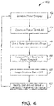
- a processing device determines the start time of downlink bursts 202 and uplink bursts 204 by analyzing power samples of a downlink portion of a TDD signal.
- a RAU 108-111 includes a downlink path separate from an uplink path.
- the downlink path includes samples of the downlink portion of a TDD signal.
- the samples in the downlink path do not include the uplink portion of the TDD signal.
- the samples in the downlink path (ideally) include only noise.
- the samples in the downlink path are I/Q samples of the downlink portion of the TDD signal.
- the processing device can generate power samples (block 402) from the I/Q samples by squaring the I/Q samples.
- Power samples are samples in which the magnitude of the data therein corresponds to the magnitude of the power in the corresponding TDD signal.
- the processing device can take the appropriate steps, if any, to generate power samples therefrom.
- the processing device can then determine a power threshold (block 404) from the power samples.
- the power threshold is determined by grouping power samples into blocks, wherein each block corresponds to a respective time period of the downlink portion of the TDD signal (also referred to herein as "downlink TDD signal").
- each block is a contiguous time period, such that all time periods of the downlink TDD signal are captured in a respective block and there is no overlap of adjacent (in TDD signal time) blocks.
- each block corresponds to 10ms of TDD signal time, such that each block includes one frame's worth of power samples.
- each block corresponds to the minimum length of time of a downlink burst in the TDD signal.
- the minimum length of time can be set in any appropriate manner such as being based on the communication protocol or based on the known minimum length of the downlink burst in the given configuration.
- the minimum length of a downlink burst is 1ms, the length of subframe.
- the processing device can then generate a set of maximum power values, wherein each maximum power value is a representation of a maximum power level for a respective block.
- the maximum power value for a block can be represented in different manners.
- the power sample having the largest value is selected as the maximum power value for a respective block.
- the maximum power value can be an estimation of the power of the largest power symbol within the block. This estimation can be obtained by filtering the power samples for the block with a moving average filter having a time period corresponding to a length of a symbol in the TDD signal. This will generate a set of filtered values for the block.
- the largest filter value from the set can be selected as the maximum power value for the block.
- other manners of representing the maximum power level for a block can be used.
- an average power can be calculated from the set of maximum power levels.
- the power threshold can then be set based on the average power.
- the power threshold can be an a priori value that is manually input.
- the processing device compares the power samples of the downlink TDD signal to the power threshold in order to identify the start of a downlink burst. Since the downlink TDD signal does not include the power from the uplink portion of the TDD signal, the power level of the downlink TDD signal should increase substantially at the start of a downlink burst and maintain a power level above a noise floor until the end of the downlink burst. By comparing the power samples of the downlink TDD signal with the power threshold, the processing device can identify the start of a downlink burst in the downlink TDD signal.
- the power threshold In order to accurately identify the start of a downlink burst in the downlink TDD signal, the power threshold should be set above the noise floor of the downlink TDD signal and below a minimum (expected) power level of the downlink burst.
- the power threshold is set at a value of one of at least 10dB, at least 6dB, or at least 3dB less than the average power determined above. In an implementation of this example, the power threshold is set at a value of 30dB less than the average power.
- the noise floor of the downlink TDD signal during an uplink burst is estimated, and the power threshold is set at a value between the average power and the noise floor.
- the noise floor can be estimated by filtering the power samples of the downlink TDD signal with a moving average filter having a time period that is slightly less than the minimum length of an uplink burst in the TDD signal.
- the minimum length of an uplink burst can be set in any appropriate manner such as being based on the communication protocol or based on the known minimum length of the uplink burst in the given configuration. In the LTD TDD protocol, the minimum length of an uplink burst is 1ms, the length of subframe.
- the time period for the moving average filter is set at between 10 and 100 percent of the minimum length of an uplink burst.
- Filtering the power samples can produce a set of filtered values.
- set of filtered values includes values corresponding to the length of a frame 200 (e.g., 10ms). The minimum of the set of filtered values can be selected as the noise floor estimate for the downlink TDD signal.
- a noise variance of the downlink TDD signal during an uplink burst time period can be estimated.
- the noise variance can be estimated from the set of power samples that were used by the filter to generate the filtered value that was selected as the noise floor estimate.
- the noise variance can be used to calculate an offset from the estimated noise floor.
- the offset can be 2, 3, or 4 sigma with respect to the estimated noise floor.
- the power threshold can then be set at the noise floor plus the offset.
- the processing device can compare power samples of the downlink TDD signal to the power threshold to determine a start of a downlink burst.
- the power samples of the downlink TDD signal are grouped into blocks (block 406).
- each block corresponds to a respective time period of the downlink TDD signal.
- each block is a contiguous time period, such that all time periods of the downlink TDD signal are captured in a respective block and there is no overlap of adjacent (in TDD signal time) blocks.
- each block is less than 1/500 th the minimum length of a downlink burst in the TDD signal.
- each block includes at least 10 samples.
- each block corresponds to 260 nanoseconds of the downlink TDD signal.
- the power samples in each block are compared to the power threshold (block 408). Based on the comparison of the samples in each block to the power threshold, each block is assigned as ON or OFF (block 410). ON is used to represent a block in which a downlink signal is present and OFF is used to represent a block in which a downlink signal is not present. If a threshold number of samples in a given block are above the power threshold, the block is assigned as ON. Otherwise, the block is assigned as OFF. In an example, the threshold number of samples is 10 percent of the samples in a block. In an implementation of this example, the threshold number of samples is 1/6 th of the samples in a block.
- the processing device can then identify a start of a downlink burst by identifying an ON block preceded by at least a minimum number of consecutive OFF blocks (block 412). Since time periods corresponding to the uplink portion of the TDD signal in the downlink TDD signal are (ideally) only noise, the blocks corresponding to these uplink time periods should be assigned as OFF. Thus, the minimum number of OFF blocks used to identify a start of a downlink burst can correspond to the minimum length of an uplink burst in the TDD signal. As discussed above, in an LTE TDD example, this minimum length can be 1ms. Thus, once a number of consecutive OFF blocks corresponding to 1ms of time are identified, the next ON block is identified as the start of a downlink burst. In this way, the start of a downlink burst can be identified by the DAS 103 based on samples of the downlink TDD signal, without demodulating and decoding the TDD signal.
- the DAS 103 can use the start to switch one or more components between downlink mode and uplink mode. For example, the duration of each downlink burst as well as the relative start times of subsequent bursts 202, 204 with the frame 200 can be input (e.g., manually) into the DAS 103 and used to calculate the start and end of each burst 202, 204 based on the identified start of one of the downlink bursts. In examples, where multiple downlink bursts 202 are included in a frame 200, the start of each of the downlink bursts 202 may need to be identified to remove ambiguity between the downlink bursts 202.
- the end of the downlink burst 202 can be determined by the one or more processing devices, for example, by identifying an OFF block following one or more ON blocks. Additionally, in some examples, a similar method to method 400 can be performed on uplink samples in the uplink path to identify a start and/or end of an uplink burst 204.
- the end of the downlink burst(s) 202 and the start and end of the uplink burst(s) 204 can be determined.
- the start and end of the respective downlink burst(s) 202 and uplink burst(s) 204 can be used to set one or more components (e.g., RAU 108, switching device 314, etc.) into downlink or uplink mode respectively.
- specifically timed uplink and/or downlink mode switching schemes can be used which, for example, switch/enable/disable some components prior to other components.
- the power amplifier 313 in the downlink path may be disabled prior to setting the switching device 314 into uplink mode to reduce the likelihood of high power signals being coupled into the uplink path.
- the above process of identifying the start of a downlink burst 202 can be implemented one or a couple times during a training mode of the DAS 103/RAU 108-111 to initially find and lock onto the start of a downlink burst 202. Once locked onto the start of a downlink burst 202, the above process can end and the DAS 103/RAU 108-111 can predict the start of subsequent bursts 202/204 based on the identified start of a downlink burst 202. In such an example, other schemes can be used to maintain the burst timing.
- the above process of identifying the start of a downlink burst 202 can be repeated continually during steady state operation with a continually updated set of blocks (updated to correspond to a more current time) to continually identify the start of a downlink burst 202 and control the one or more components accordingly.
- the above process can be used to maintain the burst timing.
- the processing device can predict the start of a downlink burst 202 based on the start of one or more previous downlink bursts 202.
- the prediction can be based on relative timing of subsequent downlink bursts 202 (e.g., the length of time between starts of downlink bursts 202) which can, for example, be input manually.
- the processing device can identify/observe the start of the subsequent downlink burst using the process described above.
- the process device can set an adjusted start of the subsequent downlink burst 202 at a time between the predicted start and the identified start.
- the adjusted start of the subsequent downlink burst 202 can then be used to control the one or more components and/or for a subsequent prediction of a later downlink burst 202.
- the adjusted start can be set at a second offset from the predicted start.
- the second offset can be selected to adjust the error in the predicted start (difference between predicted start and identified start) over multiple iterations/adjustments to reduce jitter in the adjusted start value. That is, an error of the predicted start is only partially accounted for in a given adjustment. If a subsequent determination for a subsequent downlink burst 202 indicates a further error, the error is adjusted further at that time. This iterative process continues to gradually adjust for error over multiple iterations.
- the second offset can be a fixed small increment of time (e.g., 1 microsecond).
- the second offset can be a fixed percentage of the difference between the predicted start and the identified start (e.g., 25%). In any case, tempering the adjustment of the start in this manner can reduce jitter in the adjustment, while allowing full correction of the error over multiple adjustments.
- the adjusted start can be set based on integrating the difference (error) between the predicted start and the identified start over time. Other manners of accounting for the error can also be used.
- Subsequent predicted starts for subsequent downlink bursts 202 can be determined based on the adjusted, predicted, and/or identified starts of one or more previous downlink bursts 202.
- the predicted start for a given downlink bursts 202 can be based on an averaging of an adjusted start of multiple previous downlink bursts 202 while taking into account a length of time (e.g., that is manually input) between starts of downlink bursts 202.
- the process of predicting the start, identifying the start, and setting an adjusted start can be implemented during steady state operation, and a different process can be implemented during a training phase. For example, during the training phase, larger adjustments to the predicted start can be allowed.
- the processing device can determine when to transition out of the training phase and to steady state operation based on a threshold number of successful predicted starts, that is, a threshold number of predicted starts that are sufficiently close to the corresponding identified start. In some examples, the processing device can also determine when to transition out of steady state operation and back into the training phase based on a threshold number of predicted start being sufficiently far from the corresponding identified start. In an implementation of this example, 15 consecutive successful predicted starts can be used at the threshold to determine when to transition from the training phase to steady state operation and 4 consecutive predicted starts being sufficiently far from the identified start can be used as the threshold to determine when to transition from steady state operation to the training phase.
- this process of predicting the start, identifying the start, and setting an adjusted start of a downlink burst 202 can be repeated continually to maintain the TDD timing over time.
- the process of predicting, identifying, and adjusting can be performed for all downlink bursts 202 of the TDD signal.
- the process of predicting, identifying, and adjusting can be performed for less than all (e.g., one per frame 200, one per 10 frames, etc.) of the downlink bursts 202 of the TDD signal.
- Continually identifying the start of downlink bursts 202 can include continually setting the power threshold based on a continually updated set of blocks (updated to correspond to a more current time) to continually adjust the power threshold based on the updated power samples of the TDD signal.
- the power threshold can be static after an initial training phase.
- the downlink samples can be filtered to extract one or more specific frequencies from which the timing can be obtained. Such filtering could be used, for example, to extract a reference signal from the downlink TDD signal.
Description
- Time-division duplex (TDD) methods emulate full duplex communication over a half-duplex communication link. In particular, signals that are communicated from a first device to a second device occur on the same frequencies as, but at a different time than signals communicated from the second device to the first device. Typically, one direction of communication is referred to as the "downlink" direction (and the corresponding signals are referred to here as "downlink signals" or "downlink communications"), and the other direction of communication is referred to as the "uplink" direction (and the corresponding signals are referred to here as "uplink signals" or "uplink communications"). For example, in some systems, separate downlink and uplink timeslots or sub-frames are assigned.
- Many systems use TDD for communication. For example, some implementations of the 3rd Generation Partnership Projects (3GPP) Long Term Evolution (LTE) and the Institute of Electrical and Electronics Engineers (IEEE) 802.16 standard use TDD for communication of wireless radio frequency signals.
- In order for successful communication between devices in a TDD system, the devices need to synchronize when they switch from communicating in the downlink direction to communicating in the uplink direction and when they switch from communicating in the uplink direction to communicating in the downlink direction. Otherwise, signals will be lost due to interference or missed because each device was not switched to the same signal direction.
- In some applications, a distributed antenna system (DAS) is used to relay signals between a first device and a second device in a TDD application. Such DASs, however, typically do not demodulate and decode the RF signals that they distribute. Thus, the DASs cannot determine when to switch between uplink and downlink mode based on the timing information encoded in the RF signals.
- Document
US2009/318089 discloses a method for determining timing for a time division duplex signal in a distributed antenna system according to the prior art. - The prior art document
WO 2008/076248 discloses a transition signal generator used to control a booster of a TDD signal in a communications system. The transition signal generator includes a signal sampler for sampling the TDD signal, a power detector for detecting a power of the sampled signal, and a timing control unit for generating a logic signal indicating a direction of the sampled signal from the detected power of the sampled signal.
The prior art documentU.S. 2012/0244825 discloses methods and apparatuses for performing gain control in a receiver. The methods and apparatuses receive a RF signal and obtain various counts of a number of samples of the RF signal exceeding multiple thresholds during an accumulation window. The gain of a RF gain element in the receiver is controlled based on the various counts. - The invention is as defined in the claims.
-
-
FIG. 1 is a block diagram of one embodiment of a communication system for switching between uplink and downlink transmissions; -
FIG. 2 is a diagram of one embodiment of a time division duplex (TDD) frame for use in the communication system ofFIG. 1 -
FIG. 3 is a block diagram of one embodiment of a remote antenna unit for use in the communication system ofFIG. 1 -
FIG. 4 is a flow diagram of one embodiment of a method of determining timing for a TDD signal in a distributed antenna system (DAS) in the communication system ofFIG. 1 . -
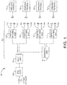
FIG. 1 is a block diagram of one embodiment of acommunication system 100.Communication system 100 is described herein as being implemented in order to distribute TDD LTE RF signals. It is to be understood, however, that other embodiments can be implemented in other ways (for example, to distribute other types of TDD RF signals, such as Wireless Broadband, WiBro, or WiMAX). As mentioned in the Background section, TDD schemes enable bi-directional communication between two devices by having uplink transmissions (fromwireless terminal 112 toward radio access network (RAN) node 102) and downlink transmissions (fromRAN node 102 toward wireless terminal 112) occur at different times using common frequencies. - In the embodiment shown in
Figure 1 ,communication system 100 comprises aRAN node 102 which is communicatively coupled to a distributed antenna system (DAS) 103. DAS 103 is used to transport communication signals between one or more upstream devices (for example,RAN node 102, wireless access points, or other sources of radio frequency signals) and one or more downstream wireless devices (for example, wireless terminals 112). In some embodiments, RANnode 102 is a part of a telecommunication-service providers' infrastructure andwireless terminals 112 comprise customer premise equipment.RAN node 102 is an RF source that performs baseband processing such as a baseband unit, a base station (e.g., eNodeB), or base transceiver station (BTS), for example. For simplicity, asingle RAN node 102 is often referred to herein, however, it should be understood that, in some embodiments, the interactions described herein can be performed withmultiple RAN nodes 102. The RF source can be a standalone unit or can be implemented as part of a centralized/cloud RAN configuration where multiple baseband units are implemented at a centralized location. -
DAS 103 comprises ahost unit 106 communicatively coupled to remote antenna units (RAUs) 108-109. In this embodiment,DAS 103 also includes anexpansion unit 114 communicatively coupled betweenhost unit 106 andRAUs host unit 106. Each remote antenna unit 108-111 is coupled to one ormore antennas 104 which are used to communicate wirelessly withwireless terminals 112. In this embodiment, each of remote antenna units 108-111 is coupled to twoantennas 104. In other embodiments, other numbers ofantennas 104 are used. Although in this embodiment a certain number of remote antenna units 108-111 andexpansion units 114 are coupled tohost unit 106, in other embodiments other numbers of remote antenna units 108-111 andexpansion units 114 are coupled tohost unit 106. Also, other DAS topologies can be used. For example, one or more host units can be daisy chained together. Also, one or more RAUs can be daisy chained together. Also, the daisy chains can form rings as well as non-ring topologies. - As shown in
Figure 1 ,host unit 106 is coupled to RAUs 108-111 andexpansion unit 114 through bi-directional point-to-point communication links. In an embodiment, communication links comprise fiber optic cables. In other embodiments, however, other communications means such as but not limited to co-axial cables, twisted pair cables (e.g., CAT-5, CAT-6 cables), or microwave communication links may be utilized in various combinations. -
Host unit 106 is communicatively coupled to one or more upstream devices (such as one ormore RAN nodes 102 or wireless access points). In some embodiments,host unit 106 is coupled to the one or more upstream devices via a physical communication medium. In other embodiments,host unit 106 is communicatively coupled to the one or more upstream devices in other ways (for example, using one or more donor antennas and one or more bi-directional amplifiers or repeaters). In an embodiment,RAN node 102 comprises an eNodeB. -
DAS 103 distributes communication signals betweenwireless terminals 112 andRAN node 102.Wireless terminals 112 transmit/receive signals to/from remote antenna units 108-111 viaremote antennas 104. - In the downlink direction, DAS 103 operates as a point-to-multipoint transport for signals from one or
more RAN nodes 102 to one or morewireless terminals 112. Downlink RAN signals are received byDAS 103 athost unit 106 from theRAN node 102. TheDAS 103 generates transport signals based on the downlink RAN signals and sends the transport signals to each of the RAUs 108-111. In an example, each of the RAUs 108-111 inDAS 103 receive identical transport signals. In other examples, one or more subsets of the RAUs 108-111 receive different transport signals. Each RAU 108-111 converts the transport signal from thehost unit 106 into an analog RF waveform and transmits the RF waveform to one or more of thewireless terminals 112 as an over-the-air modulated RF signal. Each RAU 108-111 includes a digital-to-analog converter (DAC) (in digital implementations) and radiohead hardware to perform the operations for producing the analog modulated RF waveform from the received transport signal and amplifying the analog modulated RF waveform for broadcast as an over-the-air RF signal. - In the uplink direction, each of the RAUs 108-111 senses one or more RF signals from one or more
wireless terminals 112 and generates a respective uplink transport signal based on the one or more RF signals. The RAUs 108-111 send their respective transport signals to thehost unit 106, and thehost unit 106 aggregates the information from the transport signals to provide a unified RAN signal to theRAN node 102. - The RAN signals communicated between the
RAN node 102 and DAS 103 (i.e., between theRAN node 102 and host unit 106) can be modulated analog signals or signals including digital samples corresponding to a modulated analog signal. The analog signals can be intermediate frequency (IF) or radio frequency (RF) signals. The digital samples can include samples corresponding to a baseband, intermediate frequency (IF), or radio frequency (RF) version of the RF signals. The baseband samples can be complex I/Q samples and the IF and RF samples can be real samples. The signals including digital samples corresponding to an analog modulated signal can conform to a RAN node communication protocol such as the Common Public Radio Interface (CPRI), Open Base Station Architecture Initiative (OBSAI), or Open Radio Equipment Interface (ORI). - In a digital DAS example, the transport signals sent between the
host unit 106 and the RAUs 108-111 include digital samples corresponding to the modulated analog wireless signals sent and received between the RAUs 108-111 and thewireless terminals 112. In the downlink of such an example, the transport signal is a serial data stream including the digital samples. The digital samples can include samples corresponding to a baseband, intermediate frequency (IF), or radio frequency (RF) version of the modulated analog signals. The baseband samples can be complex I/Q samples and the IF and RF samples can be real samples. - In a first implementation of a digital DAS example, the signals communicated between the
host unit 106 and theRAN node 102 are modulated analog RF signals. In the downlink of this first implementation, thehost unit 106 receives a modulated RF signal from theRAN node 102, down converts the RF signal to IF, digitizes (A/D converts) the IF signal to produce real digital IF samples, digitally down-converts the real digital IF samples to produce I/Q (complex) samples, and incorporates the I/Q samples into a downlink transport signal. In some embodiments, the I/Q samples are resampled. In some embodiments, any of the analog signals or digital samples can be filtered to select only a portion of the original bandwidth for transport. In the uplink of this first implementation, thehost unit 106 receives an uplink transport signal from one more RAUs 108-111, extracts the I/Q samples therefrom, digitally up-converts the I/Q samples to produce real digital IF samples, D/A converts the real digital IF samples to a modulated analog IF signal, up-converts the analog IF signal to an RF signal and sends the RF signal to theRAN node 102. In some embodiments, digital samples from respective transport signals can be digitally summed to form unified data for theRAN node 102. - In a second implementation of the digital DAS example, the signals communicated between the
host unit 106 and theRAN node 102 carry digital I/Q samples corresponding to a modulated analog signal. In the downlink of this second implementation, thehost unit 106 receives a signal from theRAN node 102 including digital I/Q samples (e.g., a CPRI signal) and incorporates the digital I/Q samples into a downlink transport signal to the RAUs 108-111. In some embodiments, the I/Q samples are resampled. In some embodiments, the digital samples can be filtered to select only a portion of the original bandwidth for transport. In the uplink of this second implementation, thehost unit 106 receives an uplink transport signal from one or more RAUs 108-111, extracts I/Q samples therefrom, and sends the I/Q samples to the RAN node 102 (e.g., in a CPRI signal). In some embodiments, digital samples from respective transport signals can be digitally summed to form unified data for theRAN node 102. - In any case, in a digital DAS example, the transport signals carry packets of digital samples corresponding to a modulated electromagnetic radio-frequency waveform.
- In an analog DAS example, the transport signals between the
host unit 106 and the RAUs 108-111 include a modulated analog IF signal. In such an example, thehost unit 106 can send and receive modulated analog RF signals with thehost unit 106. Thehost unit 106 can convert between the modulated RF signals and modulated analog IF signals, which are transported between thehost unit 106 and RAUs 108-111. - In some examples,
DAS 103 can be an analog and digital DAS and transport both signals including digital samples and analog modulated IF signals concurrently. - The RAUs 108-111 perform similar conversions for digital and analog DAS functions respectively. In the uplink of a digital DAS example, a
RAU 108 senses a modulated wireless RF signal via an antenna, down converts the RF signal to IF, digitizes (A/D converts) the IF signal to produce real digital IF samples, digitally down-converts the real digital IF samples to produce I/Q (complex) samples, and incorporates the I/Q samples into a downlink transport signal. In some embodiments, the I/Q samples are resampled. In some embodiments, any of the analog signals or digital samples can be filtered to select only a portion of the original bandwidth for transport. In the downlink of this digital DAS example, theRAU 108 receives an uplink transport signal from thehost unit 106, extracts the I/Q samples therefrom, digitally up-converts the I/Q samples to produce real digital IF samples, D/A converts the real digital IF samples to a modulated analog IF signal, up-converts the analog IF signal to an RF signal, amplifies and radiates a wireless RF signal to one ormore wireless terminals 112. - In an analog DAS example, the RAUs 108-111 can convert between modulated RF wireless signals to/from
wireless terminals 112 and modulated analog IF signals, which are transported between thehost unit 106 and RAUs 108-111. - In any case, for both uplink and downlink communications, the components of DAS 103 (
host unit 106,expansion unit 114, and remote antenna units 108-111) do not demodulate, decode, or deframe the signals transmitted byRAN node 102 andwireless terminals 112. -
Figure 2 illustrates one example of aTDD transmission frame 200 for use withsystem 100.Frame 200 comprises one or more downlink (DL) bursts 202 and one or more uplink (UL) bursts 204. During each downlink burst 202, downlink signals are communicated fromRAN node 102 towireless terminals 112. During each uplink burst 204, uplink signals are communicated fromwireless terminals 112 toRAN node 102. - In this embodiment, the structure of the
TDD frame 200 is static for a given channel insystem 100. That is, eachTDD frame 200 for a given channel insystem 100 has the same duration and the same number of downlink and uplink bursts having the same position and length within theirrespective frame 200. Theexample TDD frame 200 shown inFigure 2 is an example TDD LTE frame. Accordingly, the following discussion is specific to a TDD LTE frame. It should be understood, however, that other TDD frames can be used. TheTDD frame 200 has a 10ms duration and includes 10 subframes having a 1ms duration. TheTDD frame 200 includes two downlink bursts 202-1, 202-2 and two uplink bursts 204-1, 204-2. A first downlink burst 202-1 starts at the beginning of subframe #4 (4ms after the start of frame 200) and continues intosubframe # 6. A second downlink burst 202-2 starts at the beginning of subframe #9 (9ms after the start of frame 200), continues into thenext frame 200, and ends withinsubframe # 1 of thenext frame 200. A first uplink burst 204-1 starts at the beginning of subframe #2 (2ms after the start of frame 200) and continues to the end of subframe #3). A second uplink burst 204-2 starts at the beginning of subframe #7 (7ms after the start of frame 200) and continues to the end of subframe #8). - As used herein a "burst" is a portion of a TDD signal in which the TDD signal is continuous in the same direction. Thus, a downlink burst is a continuous downlink portion of the TDD signal and an uplink burst is a continuous uplink portion of the TDD signal. A continuous portion can have any structure, including one or more subframes as shown in
Figure 2 . - In LTE TDD, each (non-special) downlink subframe (e.g.,
subframes # Fig. 2 ) begins with a header/pilot time slot (DwPTS) followed by signal corresponding to payload data which extends to the end of the subframe. If adjacent (non-special) subframes are allocated to downlink signals, the TDD signal over those multiple subframes will include a header or pilot time slot at the beginning of each subframe. There is no guard period between adjacent downlink subframes. Accordingly, the downlink signal will be continuous across the adjacent downlink subframes since the signal containing payload data of a first downlink subframe will extend until the header or pilot time slot of the subsequent downlink subframe. Moreover, in TDD LTE there is a signal present during all portions of a downlink subframe. Thus, a single burst can extend across a given subframe and across multiple adjacent downlink subframes. - Special subframes (e.g.,
subframes # 1 and #6 ofFig. 2 ) start with a downlink header/pilot time slot followed by a guard period (GP) in which no downlink or uplink signals are transmitted. An uplink header/pilot time slot (UpPTS) follows the guard period and extends to the end of the special subframe. Thus, signals are not continuous across the special subframe. In TDD LTE, downlink bursts 202 end in the special subframe and uplink bursts 204 begin in a special subframe. As mentioned above, in other embodiments (e.g., in non LTE embodiments), other frame structures can be used. - The RF circuitry within
DAS 103 switches between processing downlink signals and uplink signals in coordination with the downlink bursts 202 and uplink bursts 204. The RAUs 108-111 include such RF circuitry. In an example, thehost unit 106 does not include any RF circuitry that switches with the downlink bursts 202 and uplink bursts 204. In other examples, however, thehost unit 106 can also include switching RF circuitry. -
Figure 3 is a block diagram ofexample RAU 108.RAU 108 includes one or more transport signal input/output ports 302 for sending and receiving transport signals with thehost unit 106. In the example shown inFigure 3 , the I/O ports 302 are optical ports for sending and receiving optical transport signals. In an example, the transport signals carry I/Q (complex) digital samples of a TDD signal. In an example, I/Q samples can be transported according to a serialized RF (SeRF) protocol used by ADC Telecommunications, Inc. (part of Commscope, Inc.) Shakopee, MN. In other embodiments, the I/Q samples can be transported using other transport protocols. - A first one or
more processing devices 304 can be configured to receive downlink transport signals and send uplink transport signals over the I/O ports 302. The first one ormore processing devices 304 can include a general purpose processor (GPP) or special purpose computer or processor (such as a field-programmable gate array (FPGA), application-specific integrated circuit (ASIC) or other integrated circuit), or any programmable logic device. In this example, the first one ormore processing devices 304 are disposed on a first circuit board (SeRF board). In some examples, the SeRF board is commercially available from TE Connectivity as part of the FlexWave™ line of products. The SeRF board and SeRF protocol are also described inU.S. Patent Application Serial No. 11/627,251, assigned to ADC Telecommunications, Inc. , published inU.S. Patent Application Publication No. 2008/0181282 , and incorporated herein by reference. The first one ormore processing devices 304 can be configured to generate uplink transport signals having uplink I/Q samples incorporated therein, and extract downlink I/Q samples from downlink transport signals. The uplink I/Q samples correspond to the uplink portion of a TDD signal and the downlink I/Q samples correspond to the downlink portion of the TDD signal. Although only the first one ormore processors 304 are discussed herein, it should be understood that addition components can be included on the SeRF board to implement the functionality described herein. - The I/Q samples are communicated between the first one or
more processing devices 304 and one or moreRF system processors 308 over a radio system interface (RSI) 306. The one or moreRF system processors 308 are configured to bi-directionally convert between I/Q samples and modulated analog signals for interaction with the transmitter(s) 310 and receiver(s) 312. In an example, the one or moreRF system processors 308 are configured to digitally up-convert downlink I/Q samples to real digital IF samples and to digital to analog convert the IF samples to a modulated analog IF signal which is provided to the transmitter(s) 310. The one or moreRF system processors 308 can also be configured to analog to digital convert an uplink modulated analog IF signal from the receiver(s) 312 to generate real digital IF samples and to digitally down-convert the IF samples into I/Q samples. In an example, the one or moreRF system processors 308 can also be configured to recover the timing of the TDD signal as described below. The one or moreRF system processors 308 can include a general purpose processor (GPP) or special purpose computer or processor (such as a field-programmable gate array (FPGA), application-specific integrated circuit (ASIC) or other integrated circuit), or any programmable logic device. In this example, the one or moreRF system processors 308 are disposed on a second circuit board (motherboard). Although only theRF system processors 308 are discussed herein, it should be understood that addition components can be included on the motherboard to implement the functionality described herein - The transmitter(s) 310 can be configured to up-convert the downlink modulated analog IF signal to RF. The receiver(s) 312 can be configured to down-convert an uplink modulated analog RF signal to generate an uplink modulated analog IF signal for the one or more
RF system processors 308. In some embodiments, each transmitter 310 -receiver 312pair 202 is implemented with a Digital/Analog Radio Transceiver (DART board) commercially available from ADC Telecommunications, Inc. (now part of Commscope, Inc.) of Shakopee, MN as part of the FlexWave™ Prism line of products. Each DART board can be a separate circuit board from the motherboard that is configured to plug into a port (e.g., via an edge connector) of the motherboard. The DART board is also described inU.S. Patent Application Serial No. 11/627,251, assigned to ADC Telecommunications, Inc. , published inU.S. Patent Application Publication No. 2008/01101482 - A
power amplifier 313 can be configured to amplify the downlink modulated RF signal for transmission. Aswitching device 314 can be included for each band operated on by theRAU 108 to selectively couple downlink RF signals to the antenna(s) 104 and to selectively couple uplink RF signals from the antenna(s) 104 to thereceiver 312. In an example, theswitching device 314 has two settings, a downlink setting in which the switching device is set to couple the downlink RF signal to the antenna and isolate the downlink RF signal from thereceiver 312 and an uplink setting in which the switching device is set to couple the uplink RF signal from the antenna to thereceiver 312 and to isolate the uplink RF signal from thetransmitter 310. - As described above, the
RAU 108 includes a downlink path and an uplink path. The downlink path includes a logical portion comprising the processing of the downlink digital samples (e.g., the I/Q and IF samples) and an analog portion comprising the generation of the RF modulated signal from the downlink digital samples. Likewise, the uplink path includes an analog portion comprising the generation of an analog IF signal from a sensed RF signal at antenna(s) 104 and a logical portion comprising the processing of the IF signal to generate uplink digital samples (e.g., the I/Q and IF samples). In examples where theRAU 108 operates on multiple TDD RF signals concurrently (e.g., multiple bands), a downlink path and uplink path exists for each TDD RF signal. - In an example, the
RAU 108 has an uplink mode and downlink mode for each set of downlink and uplink paths. In the uplink mode, one or more of the components are set to enable operation on the uplink signals. For example, theswitching device 314 is set to couple RF signals from the antenna(s) 104 to thereceiver 312, and thereceiver 312 can be enabled. Additionally, in the uplink mode, one or more of the components not used to process uplink signals can be disabled, such as thetransmitter 310 andpower amplifier 313. Similarly, in the downlink mode, one or more of the components are set to enable operation on the downlink signals. For example, switchingdevice 314 is set to couple the RF signals from thetransmitter 310 to the antenna(s) 104, and thetransmitter 310 andpower amplifier 313 are enabled. Additionally, in the downlink mode, one or more components not used to process downlink signals can be disabled, such as thereceiver 312. -
Wireless terminals 112 obtain the timing of the downlink bursts 202 and uplink bursts 204 by decoding downlink signals sent byRAN node 102. In particular, the downlink signals include timing information indicating when each downlink burst 202 and uplink burst 204 begins and the duration of each. TheDAS 103, however, does not demodulate and decode the signals transmitted betweenRAN node 102 andwireless terminals 112. Thus,DAS 103 independently determines the start time of the downlink bursts 202 and uplink bursts 204 in order to accurately switch between uplink mode and downlink mode. -
Figure 4 is anexample method 400 implemented by theDAS 103 to determine the start time of the downlink bursts 202 and uplink bursts 204 in aTDD frame 200. In an example, one or more "master" RAUs 108-111 implement themethod 400 to determine the timing information, and communicate the timing information to the other RAUs 108-111. In yet other examples, thehost unit 106 implements themethod 400 to determine the timing information and communicates the timing information to the RAUs 108-111. -
Method 400 is implemented by one or more processing devices. The one or more processing devices can include a general purpose processor (GPP) or special purpose computer or processor (such as a field-programmable gate array (FPGA), application-specific integrated circuit (ASIC) or other integrated circuit), or any programmable logic device. Any of the processors described above may include or function with software programs, firmware or other computer readable instructions for carrying out various methods, process tasks, calculations, and control functions, used in the digital processing functionality described herein. These instructions are typically stored on any appropriate computer readable medium used for storage of computer readable instructions or data structures. Suitable processor-readable media may include storage or memory media such as magnetic or optical media. For example, storage or memory media may include conventional hard disks, Compact Disk - Read Only Memory (CD-ROM), volatile or non-volatile media such as Random Access Memory (RAM) (including, but not limited to, Synchronous Dynamic Random Access Memory (SDRAM), Double Data Rate (DDR) RAM, RAMBUS Dynamic RAM (RDRAM), Static RAM (SRAM), etc.), Read Only Memory (ROM), Electrically Erasable Programmable ROM (EEPROM), and flash memory, etc. Suitable processor-readable media may also include transmission media such as electrical, electromagnetic, or digital signals, conveyed via a communication medium such as a network and/or a wireless like. In examples where one or more of the RAUs 108-111implements method 400, the one or moreRF system processors 308 of the RAUs 108-111 can implement themethod 400 along with suitable processor readable media and/or instructions, if desired. - For simplicity a single processing device is referred to in the following discussion. It should be understood, however, that one or more processing devices can be used to implement
method 400. Implementingmethod 400, a processing device determines the start time of downlink bursts 202 and uplink bursts 204 by analyzing power samples of a downlink portion of a TDD signal. As discussed with respect toFigure 3 , a RAU 108-111 includes a downlink path separate from an uplink path. The downlink path includes samples of the downlink portion of a TDD signal. The samples in the downlink path do not include the uplink portion of the TDD signal. Thus, at time periods allocated to uplink bursts, the samples in the downlink path (ideally) include only noise. - In an example, the samples in the downlink path are I/Q samples of the downlink portion of the TDD signal. The processing device can generate power samples (block 402) from the I/Q samples by squaring the I/Q samples. Power samples are samples in which the magnitude of the data therein corresponds to the magnitude of the power in the corresponding TDD signal. In examples where the samples in the downlink path are other than I/Q samples, the processing device can take the appropriate steps, if any, to generate power samples therefrom.
- The processing device can then determine a power threshold (block 404) from the power samples. In an example, the power threshold is determined by grouping power samples into blocks, wherein each block corresponds to a respective time period of the downlink portion of the TDD signal (also referred to herein as "downlink TDD signal"). In an implementation of this example, each block is a contiguous time period, such that all time periods of the downlink TDD signal are captured in a respective block and there is no overlap of adjacent (in TDD signal time) blocks. In an example, each block corresponds to 10ms of TDD signal time, such that each block includes one frame's worth of power samples. In another example, each block corresponds to the minimum length of time of a downlink burst in the TDD signal. The minimum length of time can be set in any appropriate manner such as being based on the communication protocol or based on the known minimum length of the downlink burst in the given configuration. In the LTD TDD protocol, the minimum length of a downlink burst is 1ms, the length of subframe.
- The processing device can then generate a set of maximum power values, wherein each maximum power value is a representation of a maximum power level for a respective block. The maximum power value for a block can be represented in different manners. In an example, the power sample having the largest value is selected as the maximum power value for a respective block. In another example, the maximum power value can be an estimation of the power of the largest power symbol within the block. This estimation can be obtained by filtering the power samples for the block with a moving average filter having a time period corresponding to a length of a symbol in the TDD signal. This will generate a set of filtered values for the block. The largest filter value from the set can be selected as the maximum power value for the block. In other example, other manners of representing the maximum power level for a block can be used.
- In any case, once a maximum power level for each block is obtained, an average power can be calculated from the set of maximum power levels. The power threshold can then be set based on the average power. In other examples, the power threshold can be an a priori value that is manually input.
- The processing device compares the power samples of the downlink TDD signal to the power threshold in order to identify the start of a downlink burst. Since the downlink TDD signal does not include the power from the uplink portion of the TDD signal, the power level of the downlink TDD signal should increase substantially at the start of a downlink burst and maintain a power level above a noise floor until the end of the downlink burst. By comparing the power samples of the downlink TDD signal with the power threshold, the processing device can identify the start of a downlink burst in the downlink TDD signal.
- In order to accurately identify the start of a downlink burst in the downlink TDD signal, the power threshold should be set above the noise floor of the downlink TDD signal and below a minimum (expected) power level of the downlink burst. In an example, the power threshold is set at a value of one of at least 10dB, at least 6dB, or at least 3dB less than the average power determined above. In an implementation of this example, the power threshold is set at a value of 30dB less than the average power.
- In another example, the noise floor of the downlink TDD signal during an uplink burst is estimated, and the power threshold is set at a value between the average power and the noise floor. The noise floor can be estimated by filtering the power samples of the downlink TDD signal with a moving average filter having a time period that is slightly less than the minimum length of an uplink burst in the TDD signal. The minimum length of an uplink burst can be set in any appropriate manner such as being based on the communication protocol or based on the known minimum length of the uplink burst in the given configuration. In the LTD TDD protocol, the minimum length of an uplink burst is 1ms, the length of subframe. In an implementation of this example, the time period for the moving average filter is set at between 10 and 100 percent of the minimum length of an uplink burst. Filtering the power samples can produce a set of filtered values. In an example, set of filtered values includes values corresponding to the length of a frame 200 (e.g., 10ms). The minimum of the set of filtered values can be selected as the noise floor estimate for the downlink TDD signal.
- In an example, to determine where between the noise floor and the average power the power threshold should be set, a noise variance of the downlink TDD signal during an uplink burst time period can be estimated. For example, the noise variance can be estimated from the set of power samples that were used by the filter to generate the filtered value that was selected as the noise floor estimate. The noise variance can be used to calculate an offset from the estimated noise floor. For example, the offset can be 2, 3, or 4 sigma with respect to the estimated noise floor. The power threshold can then be set at the noise floor plus the offset.
- In any case, the processing device can compare power samples of the downlink TDD signal to the power threshold to determine a start of a downlink burst. In order to reduce the effect of a random spike in power and to reduce the processing required, the power samples of the downlink TDD signal are grouped into blocks (block 406). In an example, each block corresponds to a respective time period of the downlink TDD signal. In an implementation of this example, each block is a contiguous time period, such that all time periods of the downlink TDD signal are captured in a respective block and there is no overlap of adjacent (in TDD signal time) blocks. In an example, each block is less than 1/500th the minimum length of a downlink burst in the TDD signal. In an implementation of this example, each block includes at least 10 samples. In a particular implementation, each block corresponds to 260 nanoseconds of the downlink TDD signal.
- The power samples in each block are compared to the power threshold (block 408). Based on the comparison of the samples in each block to the power threshold, each block is assigned as ON or OFF (block 410). ON is used to represent a block in which a downlink signal is present and OFF is used to represent a block in which a downlink signal is not present. If a threshold number of samples in a given block are above the power threshold, the block is assigned as ON. Otherwise, the block is assigned as OFF. In an example, the threshold number of samples is 10 percent of the samples in a block. In an implementation of this example, the threshold number of samples is 1/6th of the samples in a block.
- The processing device can then identify a start of a downlink burst by identifying an ON block preceded by at least a minimum number of consecutive OFF blocks (block 412). Since time periods corresponding to the uplink portion of the TDD signal in the downlink TDD signal are (ideally) only noise, the blocks corresponding to these uplink time periods should be assigned as OFF. Thus, the minimum number of OFF blocks used to identify a start of a downlink burst can correspond to the minimum length of an uplink burst in the TDD signal. As discussed above, in an LTE TDD example, this minimum length can be 1ms. Thus, once a number of consecutive OFF blocks corresponding to 1ms of time are identified, the next ON block is identified as the start of a downlink burst. In this way, the start of a downlink burst can be identified by the
DAS 103 based on samples of the downlink TDD signal, without demodulating and decoding the TDD signal. - Once the start of a
downlink burst 202 is identified, theDAS 103 can use the start to switch one or more components between downlink mode and uplink mode. For example, the duration of each downlink burst as well as the relative start times ofsubsequent bursts frame 200 can be input (e.g., manually) into theDAS 103 and used to calculate the start and end of each burst 202, 204 based on the identified start of one of the downlink bursts. In examples, where multiple downlink bursts 202 are included in aframe 200, the start of each of the downlink bursts 202 may need to be identified to remove ambiguity between the downlink bursts 202. In other examples, the end of the downlink burst 202 can be determined by the one or more processing devices, for example, by identifying an OFF block following one or more ON blocks. Additionally, in some examples, a similar method tomethod 400 can be performed on uplink samples in the uplink path to identify a start and/or end of anuplink burst 204. - In any case, once the start of a (or multiple) downlink burst(s) 202 is identified, the end of the downlink burst(s) 202 and the start and end of the uplink burst(s) 204 can be determined. The start and end of the respective downlink burst(s) 202 and uplink burst(s) 204 can be used to set one or more components (e.g.,
RAU 108, switchingdevice 314, etc.) into downlink or uplink mode respectively. In some examples, specifically timed uplink and/or downlink mode switching schemes can be used which, for example, switch/enable/disable some components prior to other components. For example, thepower amplifier 313 in the downlink path may be disabled prior to setting theswitching device 314 into uplink mode to reduce the likelihood of high power signals being coupled into the uplink path. - In an example, the above process of identifying the start of a
downlink burst 202 can be implemented one or a couple times during a training mode of theDAS 103/RAU 108-111 to initially find and lock onto the start of adownlink burst 202. Once locked onto the start of adownlink burst 202, the above process can end and theDAS 103/RAU 108-111 can predict the start ofsubsequent bursts 202/204 based on the identified start of adownlink burst 202. In such an example, other schemes can be used to maintain the burst timing. - In an alternative example, the above process of identifying the start of a
downlink burst 202 can be repeated continually during steady state operation with a continually updated set of blocks (updated to correspond to a more current time) to continually identify the start of adownlink burst 202 and control the one or more components accordingly. In such an alternative example, the above process can be used to maintain the burst timing. - In an implementation of such an alternative example, the processing device can predict the start of a
downlink burst 202 based on the start of one or more previous downlink bursts 202. The prediction can be based on relative timing of subsequent downlink bursts 202 (e.g., the length of time between starts of downlink bursts 202) which can, for example, be input manually. In addition to predicting the start of a subsequent downlink burst 202, the processing device can identify/observe the start of the subsequent downlink burst using the process described above. If there is a difference between the predicted start of the subsequent downlink burst 202 and the identified start of the subsequent downlink burst 202, the process device can set an adjusted start of the subsequent downlink burst 202 at a time between the predicted start and the identified start. The adjusted start of the subsequent downlink burst 202 can then be used to control the one or more components and/or for a subsequent prediction of a later downlink burst 202. - In an example, the adjusted start can be set at a second offset from the predicted start. The second offset can be selected to adjust the error in the predicted start (difference between predicted start and identified start) over multiple iterations/adjustments to reduce jitter in the adjusted start value. That is, an error of the predicted start is only partially accounted for in a given adjustment. If a subsequent determination for a subsequent downlink burst 202 indicates a further error, the error is adjusted further at that time. This iterative process continues to gradually adjust for error over multiple iterations. In an example, the second offset can be a fixed small increment of time (e.g., 1 microsecond). In another example, the second offset can be a fixed percentage of the difference between the predicted start and the identified start (e.g., 25%). In any case, tempering the adjustment of the start in this manner can reduce jitter in the adjustment, while allowing full correction of the error over multiple adjustments.
- In another example, the adjusted start can be set based on integrating the difference (error) between the predicted start and the identified start over time. Other manners of accounting for the error can also be used.
- Subsequent predicted starts for subsequent downlink bursts 202 can be determined based on the adjusted, predicted, and/or identified starts of one or more previous downlink bursts 202. For example, the predicted start for a given downlink bursts 202 can be based on an averaging of an adjusted start of multiple previous downlink bursts 202 while taking into account a length of time (e.g., that is manually input) between starts of downlink bursts 202.
- In some examples, the process of predicting the start, identifying the start, and setting an adjusted start can be implemented during steady state operation, and a different process can be implemented during a training phase. For example, during the training phase, larger adjustments to the predicted start can be allowed. The processing device can determine when to transition out of the training phase and to steady state operation based on a threshold number of successful predicted starts, that is, a threshold number of predicted starts that are sufficiently close to the corresponding identified start. In some examples, the processing device can also determine when to transition out of steady state operation and back into the training phase based on a threshold number of predicted start being sufficiently far from the corresponding identified start. In an implementation of this example, 15 consecutive successful predicted starts can be used at the threshold to determine when to transition from the training phase to steady state operation and 4 consecutive predicted starts being sufficiently far from the identified start can be used as the threshold to determine when to transition from steady state operation to the training phase.
- As indicated above, this process of predicting the start, identifying the start, and setting an adjusted start of a
downlink burst 202 can be repeated continually to maintain the TDD timing over time. In an implementation of this example, the process of predicting, identifying, and adjusting can be performed for all downlink bursts 202 of the TDD signal. In another implementation of this example, the process of predicting, identifying, and adjusting can be performed for less than all (e.g., one perframe 200, one per 10 frames, etc.) of the downlink bursts 202 of the TDD signal. - Continually identifying the start of downlink bursts 202 can include continually setting the power threshold based on a continually updated set of blocks (updated to correspond to a more current time) to continually adjust the power threshold based on the updated power samples of the TDD signal. In other examples, the power threshold can be static after an initial training phase.
- In some examples, other operations can be performed on the downlink samples prior to generating power samples therefrom and/or analyzing the power samples to identify a start of a
downlink burst 202. For example, the downlink samples can be filtered to extract one or more specific frequencies from which the timing can be obtained. Such filtering could be used, for example, to extract a reference signal from the downlink TDD signal.
Claims (15)
- A unit for a distributed antenna system, DAS (103), wherein the unit is a host unit (106) or a master remote antenna unit (108), the unit comprising:one or more processing devices configured to:
group power samples of a downlink portion of the TDD signal into blocks corresponding to a respective time period;compare power samples of the blocks to a power threshold;assign the blocks as ON or OFF based on a number of power samples in a respective block that are above the power threshold;identify a start of a downlink burst in the TDD signal as an ON block preceded by at least a minimum number of consecutive OFF blocks; andsend timing information for when to switch RF circuitry to one or more remote antenna units (108, 109, 110, 111) of the DAS (103) based on the start of the downlink burst. - The unit of claim 1, wherein each block corresponds to a common length of time, and optionally,
wherein the common length of time is less than 1/500th a minimum length of a downlink burst in the TDD signal, wherein the common length of time corresponds to at least 10 samples, wherein each block corresponds to a contiguous time period. - The unit of any of claims 1-2, wherein the one or more processing devices are configured to generate the power samples by squaring complex data samples.
- The unit of any of claims 1-3, wherein the one or more processing devices are configured to assign the respective block as ON if more than a minimum number of power samples in the respective block are above the power threshold, and optionally, wherein the minimum number of power samples is at least 10 percent of the power samples in the respective block.
- The unit of any of claims 1-4, wherein the minimum number of consecutive OFF blocks is less than or equal to a number of blocks corresponding to the minimum length of an uplink burst in the TDD signal.
- The unit of any of claims 1-5, wherein the one or more processing devices are configured to continually adjust the power threshold based on power samples of the TDD signal.
- The unit of claim 6, wherein the one or more processing devices are configured to:group power samples of the downlink portion of the TDD signal into second blocks corresponding to a respective time period;generate a set of maximum power values, the set of maximum power values consisting of a maximum power value for each of a contiguous set of the second blocks;calculate an average power of the set of maximum power values; andset the power threshold based on the average power.
- The unit of claim 7, wherein the one or more processing devices are configured to select the largest power sample from each of the second blocks in the contiguous set as the maximum power value for that second block.
- The unit of claim 8, wherein the one or more processing devices are configured to, for each of the second blocks in the contiguous set:filter the power samples for a respective block with a moving average filter having a time period corresponding to a length of a symbol of the TDD signal to generate a set of filtered values for the respective block; andselect the largest filtered value for the respective block as the maximum power value for the respective block.
- The unit of claim 7, wherein the one or more processing devices are configured to group the power samples into blocks having a common length of time that is at least the minimum length of time of a downlink burst in the TDD signal, and optionally, wherein the one or more processing devices are configured to set the power threshold includes setting the power threshold at a value at least 3dB less than the average power.
- The unit of claim 7, wherein the one or more processing devices are configured to:estimate a noise floor of the downlink portion of the TDD signal during an uplink burst time period; andset the power threshold at a value between the average power and the noise floor.
- The unit of any of claims 1-11, wherein the one or more processing devices are configured to:determine the number of consecutive ON blocks from the start of the downlink burst; andif the number of consecutive ON blocks does not equal an expected duration of the downlink burst, set an alarm.
- The unit of any of claims 1-12, wherein the one or more processing devices are configured to:predict a start of the downlink burst based on a start of one or more previous downlink bursts;if the identified start of the downlink burst is different than the predicted start of the downlink burst, set an adjusted start for the downlink burst at a time between the predicted start and the identified start; andsend timing information to one or more remote antenna units (108, 109, 110, 111) of the DAS (103) based on the adjusted start.
- The unit of any of claims 1-13, wherein the unit is a master remote antenna unit, wherein the unit includes:one or more antennas (104) for radiation of downlink signals and for sensing of uplink signals;a switch (314) configured to selectively couple one of a downlink communication path or an uplink communication path to the one or more antennas (104).
- The unit of any of claims 1-13, wherein the unit is a host unit (106), wherein the unit further includes:an interface configured to be coupled to a radio access network node (102) or a wireless access point; andone or more ports configured to be coupled to the one or more remote antenna units (108, 109, 110, 111).
Applications Claiming Priority (3)
| Application Number | Priority Date | Filing Date | Title |
|---|---|---|---|
| US201562236870P | 2015-10-03 | 2015-10-03 | |
| EP16852831.3A EP3357166B1 (en) | 2015-10-03 | 2016-10-03 | Tdd timing recovery in a distributed antenna system |
| PCT/US2016/055184 WO2017059435A1 (en) | 2015-10-03 | 2016-10-03 | Tdd timing recovery in a distributed antenna system |
Related Parent Applications (1)
| Application Number | Title | Priority Date | Filing Date |
|---|---|---|---|
| EP16852831.3A Division EP3357166B1 (en) | 2015-10-03 | 2016-10-03 | Tdd timing recovery in a distributed antenna system |
Publications (2)
| Publication Number | Publication Date |
|---|---|
| EP3761525A1 EP3761525A1 (en) | 2021-01-06 |
| EP3761525B1 true EP3761525B1 (en) | 2023-01-04 |
Family
ID=58427959
Family Applications (2)
| Application Number | Title | Priority Date | Filing Date |
|---|---|---|---|
| EP16852831.3A Active EP3357166B1 (en) | 2015-10-03 | 2016-10-03 | Tdd timing recovery in a distributed antenna system |
| EP20191953.7A Active EP3761525B1 (en) | 2015-10-03 | 2016-10-03 | Tdd timing recovery in a distributed antenna system |
Family Applications Before (1)
| Application Number | Title | Priority Date | Filing Date |
|---|---|---|---|
| EP16852831.3A Active EP3357166B1 (en) | 2015-10-03 | 2016-10-03 | Tdd timing recovery in a distributed antenna system |
Country Status (4)
| Country | Link |
|---|---|
| US (1) | US10673604B2 (en) |
| EP (2) | EP3357166B1 (en) |
| CN (1) | CN108352854B (en) |
| WO (1) | WO2017059435A1 (en) |
Families Citing this family (10)
| Publication number | Priority date | Publication date | Assignee | Title |
|---|---|---|---|---|
| WO2018004411A1 (en) * | 2016-07-01 | 2018-01-04 | Telefonaktiebolaget Lm Ericsson (Publ) | Over the air testing of a radio communications device |
| US10454571B2 (en) * | 2017-07-20 | 2019-10-22 | Corning Optical Communications LLC | Dynamic determination of threshold power level for use in distinguishing between downlink and uplink periods in time-division duplexed (TDD) communications |
| US20210029564A1 (en) * | 2018-05-17 | 2021-01-28 | Andrew Wireless Systems Gmbh | User equipment assisted leveling and optimization of distributed antenna systems |
| CN109361416B (en) * | 2018-10-31 | 2020-07-28 | 深圳昂瑞微电子技术有限公司 | Symbol timing recovery circuit and receiver thereof |
| US10616005B1 (en) * | 2018-11-28 | 2020-04-07 | Samsung Electronics Co., Ltd. | Robust noise power estimation |
| EP3991323A4 (en) | 2019-09-13 | 2023-06-21 | CommScope Technologies LLC | Repeater system for use with 5g new radio base station that uses time-division duplexing |
| US11956185B2 (en) | 2020-04-15 | 2024-04-09 | Corning Research & Development Corporation | Time-division duplexing (TDD) detection in wireless distributed communications systems (DCS) to synchronize TDD downlink and uplink communications, and related methods |
| US11503554B2 (en) * | 2020-05-13 | 2022-11-15 | Sprint Spectrum L.P. | Dynamically accounting for past transmit power as basis to set future transmit power on co-existing air interface |
| WO2023239544A1 (en) * | 2022-06-09 | 2023-12-14 | Commscope Technologies Llc | Techniques about converting time-domain fronthaul data to frequency-domain fronthaul data within a distributed antenna system |
| WO2023241805A1 (en) * | 2022-06-16 | 2023-12-21 | Telefonaktiebolaget Lm Ericsson (Publ) | Method and apparatus for power level determination by analyzing an occurence of received power sample values during a time interval |
Family Cites Families (24)
| Publication number | Priority date | Publication date | Assignee | Title |
|---|---|---|---|---|
| JP4960223B2 (en) | 2004-05-13 | 2012-06-27 | クゥアルコム・インコーポレイテッド | Non-frequency conversion repeater for detection and media access control |
| JP5107997B2 (en) | 2006-03-31 | 2012-12-26 | クゥアルコム・インコーポレイテッド | Enhanced physical layer repeater for operation within the WiMAX system |
| EP2103002B1 (en) * | 2006-12-13 | 2016-07-27 | Intel Corporation | Time division duplex forward-to-reverse transition signal generator |
| US8737454B2 (en) | 2007-01-25 | 2014-05-27 | Adc Telecommunications, Inc. | Modular wireless communications platform |
| US8437792B2 (en) * | 2007-02-14 | 2013-05-07 | Qualcomm Incorporated | Uplink power control for LTE |
| US8165100B2 (en) * | 2007-12-21 | 2012-04-24 | Powerwave Technologies, Inc. | Time division duplexed digital distributed antenna system |
| DE102008017881B9 (en) | 2008-04-09 | 2012-11-08 | Andrew Wireless Systems Gmbh | TDD repeater for a wireless network and method for operating such a repeater |
| US8385373B2 (en) | 2008-06-24 | 2013-02-26 | Adc Telecommunications, Inc. | Method and apparatus for frame detection in a communications system |
| US8208414B2 (en) | 2008-06-24 | 2012-06-26 | Lgc Wireless, Inc. | System and method for configurable time-division duplex interface |
| US8310963B2 (en) | 2008-06-24 | 2012-11-13 | Adc Telecommunications, Inc. | System and method for synchronized time-division duplex signal switching |
| US8626238B2 (en) * | 2008-06-24 | 2014-01-07 | Adc Telecommunications, Inc. | Method and apparatus for switching in a TDD system |
| US7961689B2 (en) | 2008-08-18 | 2011-06-14 | Adc Telecommunications, Inc. | Method and apparatus for determining an end of a subframe in a TDD system |
| AT13329U1 (en) | 2008-10-27 | 2013-10-15 | Andrew Wireless Systems Gmbh | Repeater and method for operating such a repeater |
| US8050246B2 (en) | 2009-03-03 | 2011-11-01 | Adc Telecommunications, Inc. | Range extension for time division duplex systems |
| KR101508978B1 (en) * | 2009-04-20 | 2015-04-07 | 주식회사 케이엠더블유 | Method for controling transmit/receive timing of base station antenna in tdd wireless communication and apparatus therefor the the same |
| CN103210598B (en) * | 2010-08-13 | 2017-03-22 | 爱立信(中国)通信有限公司 | Automatic guard period adjustment in a base station for time division duplexed wireless communications |
| CN102404761B (en) * | 2010-09-15 | 2014-02-05 | 联芯科技有限公司 | Maintaining of synchronization timing for TD (Time Division) and method and device for carrying out disparate system measurement |
| US9172344B2 (en) | 2011-03-24 | 2015-10-27 | Silicon Laboratories Inc. | Statistical gain control in a receiver |
| US8693342B2 (en) | 2011-10-28 | 2014-04-08 | Adc Telecommunications, Inc. | Distributed antenna system using time division duplexing scheme |
| WO2014199380A1 (en) | 2013-06-12 | 2014-12-18 | Corning Optical Communications Wireless, Ltd. | Time-division duplexing (tdd) in distributed communications systems, including distributed antenna systems (dass) |
| WO2015029021A1 (en) | 2013-08-29 | 2015-03-05 | Corning Optical Communications Wireless Ltd. | Detecting uplink/downlink time-division duplexed (tdd) frame configurations to synchronize tdd downlink and uplink communications between tdd communications equipment |
| EP3064031B1 (en) * | 2013-10-30 | 2019-05-08 | Andrew Wireless Systems GmbH | Switching sub-system for distributed antenna systems using time division duplexing |
| AU2015244008B2 (en) * | 2014-04-11 | 2019-01-17 | Commscope Technologies Llc | Frequency-division duplexing in a time-division duplexing mode for a telecommunications system |
| CN107409367B (en) * | 2015-02-20 | 2020-12-01 | 瑞典爱立信有限公司 | Radio unit for controlling power levels of spatially separated transceivers in a wireless communication network and method therein |
-
2016
- 2016-10-03 WO PCT/US2016/055184 patent/WO2017059435A1/en active Application Filing
- 2016-10-03 US US15/765,712 patent/US10673604B2/en active Active
- 2016-10-03 EP EP16852831.3A patent/EP3357166B1/en active Active
- 2016-10-03 EP EP20191953.7A patent/EP3761525B1/en active Active
- 2016-10-03 CN CN201680066654.1A patent/CN108352854B/en active Active
Also Published As
| Publication number | Publication date |
|---|---|
| US20180302210A1 (en) | 2018-10-18 |
| EP3357166B1 (en) | 2020-09-02 |
| US10673604B2 (en) | 2020-06-02 |
| EP3761525A1 (en) | 2021-01-06 |
| CN108352854A (en) | 2018-07-31 |
| WO2017059435A1 (en) | 2017-04-06 |
| EP3357166A1 (en) | 2018-08-08 |
| EP3357166A4 (en) | 2019-05-29 |
| CN108352854B (en) | 2020-09-04 |
Similar Documents
| Publication | Publication Date | Title |
|---|---|---|
| EP3761525B1 (en) | Tdd timing recovery in a distributed antenna system | |
| CN113055136B (en) | Method and terminal for configuring and receiving transmission resources of positioning reference signals | |
| EP2319203B1 (en) | Method and apparatus for determining an end of a subframe in a tdd system | |
| CN107528628B (en) | Signal synchronization method, device and system of satellite communication system | |
| US10187239B2 (en) | Systems and methods to reduce the peak-to-average power ratio (PAPR) of signals in channel bonding | |
| EP3909336B1 (en) | Remote interference mitigation resource configuration | |
| US9980318B2 (en) | DAS management by radio access network node | |
| CN111434070B (en) | Method and network node for supporting full-duplex communication | |
| US11528671B2 (en) | Frame structure to support long distance transmission | |
| US10720989B2 (en) | Apparatus and method for transmitting and receiving signal in communication system | |
| US20080137561A1 (en) | Rf repeater used for time division duplexing and method thereof | |
| US10250370B2 (en) | Frame structure for a physical control channel | |
| JP6121270B2 (en) | Distributed radio communication base station system, signal processing apparatus, radio apparatus, and optical section signal distortion estimation method | |
| US10652059B2 (en) | Mission critical wireless communication link master gateway | |
| US11038736B2 (en) | Method for cancelling self-interference signal when operating in FDR mode, and device therefor | |
| CN114651515A (en) | Dual root preamble design for delay and frequency shift | |
| US20230389005A1 (en) | User equipment indication of preferred timing adjustment | |
| EP3573255B1 (en) | Repeater and operating method of the repeater | |
| CN103051372B (en) | Synchronization method and device of WiMAX (Worldwide Interoperability for Microwave Access) repeater | |
| CN109923908B (en) | Modified multi-gap extended coverage random access channel transmission | |
| CN109076470B (en) | Signal transmission method, device and system | |
| WO2023141061A2 (en) | Enhanced automatic gain control for full-duplex in millimeter wave systems | |
| WO2023225442A1 (en) | Automatic gain control for super-high order modulations | |
| WO2023158899A1 (en) | Slot structure for automatic gain control for high subcarrier spacing | |
| CN117223245A (en) | Techniques for determining characteristics of signals forwarded by wireless devices |
Legal Events
| Date | Code | Title | Description |
|---|---|---|---|
| PUAI | Public reference made under article 153(3) epc to a published international application that has entered the european phase |
Free format text: ORIGINAL CODE: 0009012 |
|
| STAA | Information on the status of an ep patent application or granted ep patent |
Free format text: STATUS: THE APPLICATION HAS BEEN PUBLISHED |
|
| AC | Divisional application: reference to earlier application |
Ref document number: 3357166 Country of ref document: EP Kind code of ref document: P |
|
| AK | Designated contracting states |
Kind code of ref document: A1 Designated state(s): AL AT BE BG CH CY CZ DE DK EE ES FI FR GB GR HR HU IE IS IT LI LT LU LV MC MK MT NL NO PL PT RO RS SE SI SK SM TR |
|
| RAP1 | Party data changed (applicant data changed or rights of an application transferred) |
Owner name: COMMSCOPE TECHNOLOGIES LLC |
|
| STAA | Information on the status of an ep patent application or granted ep patent |
Free format text: STATUS: REQUEST FOR EXAMINATION WAS MADE |
|
| 17P | Request for examination filed |
Effective date: 20210706 |
|
| RBV | Designated contracting states (corrected) |
Designated state(s): AL AT BE BG CH CY CZ DE DK EE ES FI FR GB GR HR HU IE IS IT LI LT LU LV MC MK MT NL NO PL PT RO RS SE SI SK SM TR |
|
| GRAP | Despatch of communication of intention to grant a patent |
Free format text: ORIGINAL CODE: EPIDOSNIGR1 |
|
| STAA | Information on the status of an ep patent application or granted ep patent |
Free format text: STATUS: GRANT OF PATENT IS INTENDED |
|
| INTG | Intention to grant announced |
Effective date: 20220905 |
|
| GRAS | Grant fee paid |
Free format text: ORIGINAL CODE: EPIDOSNIGR3 |
|
| GRAA | (expected) grant |
Free format text: ORIGINAL CODE: 0009210 |
|
| STAA | Information on the status of an ep patent application or granted ep patent |
Free format text: STATUS: THE PATENT HAS BEEN GRANTED |
|
| AC | Divisional application: reference to earlier application |
Ref document number: 3357166 Country of ref document: EP Kind code of ref document: P |
|
| AK | Designated contracting states |
Kind code of ref document: B1 Designated state(s): AL AT BE BG CH CY CZ DE DK EE ES FI FR GB GR HR HU IE IS IT LI LT LU LV MC MK MT NL NO PL PT RO RS SE SI SK SM TR |
|
| REG | Reference to a national code |
Ref country code: GB Ref legal event code: FG4D |
|
| REG | Reference to a national code |
Ref country code: CH Ref legal event code: EP |
|
| REG | Reference to a national code |
Ref country code: AT Ref legal event code: REF Ref document number: 1542672 Country of ref document: AT Kind code of ref document: T Effective date: 20230115 |
|
| REG | Reference to a national code |
Ref country code: DE Ref legal event code: R096 Ref document number: 602016077365 Country of ref document: DE |
|
| REG | Reference to a national code |
Ref country code: IE Ref legal event code: FG4D |
|
| REG | Reference to a national code |
Ref country code: LT Ref legal event code: MG9D |
|
| REG | Reference to a national code |
Ref country code: NL Ref legal event code: MP Effective date: 20230104 |
|
| REG | Reference to a national code |
Ref country code: AT Ref legal event code: MK05 Ref document number: 1542672 Country of ref document: AT Kind code of ref document: T Effective date: 20230104 |
|
| PG25 | Lapsed in a contracting state [announced via postgrant information from national office to epo] |
Ref country code: NL Free format text: LAPSE BECAUSE OF FAILURE TO SUBMIT A TRANSLATION OF THE DESCRIPTION OR TO PAY THE FEE WITHIN THE PRESCRIBED TIME-LIMIT Effective date: 20230104 |
|
| P01 | Opt-out of the competence of the unified patent court (upc) registered |
Effective date: 20230530 |
|
| PG25 | Lapsed in a contracting state [announced via postgrant information from national office to epo] |
Ref country code: RS Free format text: LAPSE BECAUSE OF FAILURE TO SUBMIT A TRANSLATION OF THE DESCRIPTION OR TO PAY THE FEE WITHIN THE PRESCRIBED TIME-LIMIT Effective date: 20230104 Ref country code: PT Free format text: LAPSE BECAUSE OF FAILURE TO SUBMIT A TRANSLATION OF THE DESCRIPTION OR TO PAY THE FEE WITHIN THE PRESCRIBED TIME-LIMIT Effective date: 20230504 Ref country code: NO Free format text: LAPSE BECAUSE OF FAILURE TO SUBMIT A TRANSLATION OF THE DESCRIPTION OR TO PAY THE FEE WITHIN THE PRESCRIBED TIME-LIMIT Effective date: 20230404 Ref country code: LV Free format text: LAPSE BECAUSE OF FAILURE TO SUBMIT A TRANSLATION OF THE DESCRIPTION OR TO PAY THE FEE WITHIN THE PRESCRIBED TIME-LIMIT Effective date: 20230104 Ref country code: LT Free format text: LAPSE BECAUSE OF FAILURE TO SUBMIT A TRANSLATION OF THE DESCRIPTION OR TO PAY THE FEE WITHIN THE PRESCRIBED TIME-LIMIT Effective date: 20230104 Ref country code: HR Free format text: LAPSE BECAUSE OF FAILURE TO SUBMIT A TRANSLATION OF THE DESCRIPTION OR TO PAY THE FEE WITHIN THE PRESCRIBED TIME-LIMIT Effective date: 20230104 Ref country code: ES Free format text: LAPSE BECAUSE OF FAILURE TO SUBMIT A TRANSLATION OF THE DESCRIPTION OR TO PAY THE FEE WITHIN THE PRESCRIBED TIME-LIMIT Effective date: 20230104 Ref country code: AT Free format text: LAPSE BECAUSE OF FAILURE TO SUBMIT A TRANSLATION OF THE DESCRIPTION OR TO PAY THE FEE WITHIN THE PRESCRIBED TIME-LIMIT Effective date: 20230104 |
|
| PG25 | Lapsed in a contracting state [announced via postgrant information from national office to epo] |
Ref country code: SE Free format text: LAPSE BECAUSE OF FAILURE TO SUBMIT A TRANSLATION OF THE DESCRIPTION OR TO PAY THE FEE WITHIN THE PRESCRIBED TIME-LIMIT Effective date: 20230104 Ref country code: PL Free format text: LAPSE BECAUSE OF FAILURE TO SUBMIT A TRANSLATION OF THE DESCRIPTION OR TO PAY THE FEE WITHIN THE PRESCRIBED TIME-LIMIT Effective date: 20230104 Ref country code: IS Free format text: LAPSE BECAUSE OF FAILURE TO SUBMIT A TRANSLATION OF THE DESCRIPTION OR TO PAY THE FEE WITHIN THE PRESCRIBED TIME-LIMIT Effective date: 20230504 Ref country code: GR Free format text: LAPSE BECAUSE OF FAILURE TO SUBMIT A TRANSLATION OF THE DESCRIPTION OR TO PAY THE FEE WITHIN THE PRESCRIBED TIME-LIMIT Effective date: 20230405 Ref country code: FI Free format text: LAPSE BECAUSE OF FAILURE TO SUBMIT A TRANSLATION OF THE DESCRIPTION OR TO PAY THE FEE WITHIN THE PRESCRIBED TIME-LIMIT Effective date: 20230104 |
|
| REG | Reference to a national code |
Ref country code: DE Ref legal event code: R097 Ref document number: 602016077365 Country of ref document: DE |
|
| PG25 | Lapsed in a contracting state [announced via postgrant information from national office to epo] |
Ref country code: SM Free format text: LAPSE BECAUSE OF FAILURE TO SUBMIT A TRANSLATION OF THE DESCRIPTION OR TO PAY THE FEE WITHIN THE PRESCRIBED TIME-LIMIT Effective date: 20230104 Ref country code: RO Free format text: LAPSE BECAUSE OF FAILURE TO SUBMIT A TRANSLATION OF THE DESCRIPTION OR TO PAY THE FEE WITHIN THE PRESCRIBED TIME-LIMIT Effective date: 20230104 Ref country code: EE Free format text: LAPSE BECAUSE OF FAILURE TO SUBMIT A TRANSLATION OF THE DESCRIPTION OR TO PAY THE FEE WITHIN THE PRESCRIBED TIME-LIMIT Effective date: 20230104 Ref country code: DK Free format text: LAPSE BECAUSE OF FAILURE TO SUBMIT A TRANSLATION OF THE DESCRIPTION OR TO PAY THE FEE WITHIN THE PRESCRIBED TIME-LIMIT Effective date: 20230104 Ref country code: CZ Free format text: LAPSE BECAUSE OF FAILURE TO SUBMIT A TRANSLATION OF THE DESCRIPTION OR TO PAY THE FEE WITHIN THE PRESCRIBED TIME-LIMIT Effective date: 20230104 |
|
| PLBE | No opposition filed within time limit |
Free format text: ORIGINAL CODE: 0009261 |
|
| STAA | Information on the status of an ep patent application or granted ep patent |
Free format text: STATUS: NO OPPOSITION FILED WITHIN TIME LIMIT |
|
| PG25 | Lapsed in a contracting state [announced via postgrant information from national office to epo] |
Ref country code: SK Free format text: LAPSE BECAUSE OF FAILURE TO SUBMIT A TRANSLATION OF THE DESCRIPTION OR TO PAY THE FEE WITHIN THE PRESCRIBED TIME-LIMIT Effective date: 20230104 |
|
| 26N | No opposition filed |
Effective date: 20231005 |
|
| PGFP | Annual fee paid to national office [announced via postgrant information from national office to epo] |
Ref country code: GB Payment date: 20231027 Year of fee payment: 8 |
|
| PG25 | Lapsed in a contracting state [announced via postgrant information from national office to epo] |
Ref country code: SI Free format text: LAPSE BECAUSE OF FAILURE TO SUBMIT A TRANSLATION OF THE DESCRIPTION OR TO PAY THE FEE WITHIN THE PRESCRIBED TIME-LIMIT Effective date: 20230104 |
|
| PGFP | Annual fee paid to national office [announced via postgrant information from national office to epo] |
Ref country code: IT Payment date: 20231023 Year of fee payment: 8 Ref country code: FR Payment date: 20231025 Year of fee payment: 8 Ref country code: DE Payment date: 20231027 Year of fee payment: 8 |