EP3761512A1 - Dynamic common mode control - Google Patents
Dynamic common mode control Download PDFInfo
- Publication number
- EP3761512A1 EP3761512A1 EP20182769.8A EP20182769A EP3761512A1 EP 3761512 A1 EP3761512 A1 EP 3761512A1 EP 20182769 A EP20182769 A EP 20182769A EP 3761512 A1 EP3761512 A1 EP 3761512A1
- Authority
- EP
- European Patent Office
- Prior art keywords
- signal
- offset
- input signal
- common mode
- differential
- Prior art date
- Legal status (The legal status is an assumption and is not a legal conclusion. Google has not performed a legal analysis and makes no representation as to the accuracy of the status listed.)
- Granted
Links
Images




Classifications
-
- H—ELECTRICITY
- H03—ELECTRONIC CIRCUITRY
- H03F—AMPLIFIERS
- H03F3/00—Amplifiers with only discharge tubes or only semiconductor devices as amplifying elements
- H03F3/45—Differential amplifiers
- H03F3/45071—Differential amplifiers with semiconductor devices only
- H03F3/45076—Differential amplifiers with semiconductor devices only characterised by the way of implementation of the active amplifying circuit in the differential amplifier
- H03F3/45475—Differential amplifiers with semiconductor devices only characterised by the way of implementation of the active amplifying circuit in the differential amplifier using IC blocks as the active amplifying circuit
-
- H—ELECTRICITY
- H03—ELECTRONIC CIRCUITRY
- H03M—CODING; DECODING; CODE CONVERSION IN GENERAL
- H03M1/00—Analogue/digital conversion; Digital/analogue conversion
- H03M1/12—Analogue/digital converters
- H03M1/124—Sampling or signal conditioning arrangements specially adapted for A/D converters
- H03M1/129—Means for adapting the input signal to the range the converter can handle, e.g. limiting, pre-scaling ; Out-of-range indication
-
- H—ELECTRICITY
- H03—ELECTRONIC CIRCUITRY
- H03M—CODING; DECODING; CODE CONVERSION IN GENERAL
- H03M1/00—Analogue/digital conversion; Digital/analogue conversion
- H03M1/66—Digital/analogue converters
-
- H—ELECTRICITY
- H03—ELECTRONIC CIRCUITRY
- H03M—CODING; DECODING; CODE CONVERSION IN GENERAL
- H03M1/00—Analogue/digital conversion; Digital/analogue conversion
- H03M1/06—Continuously compensating for, or preventing, undesired influence of physical parameters
- H03M1/0602—Continuously compensating for, or preventing, undesired influence of physical parameters of deviations from the desired transfer characteristic
- H03M1/0604—Continuously compensating for, or preventing, undesired influence of physical parameters of deviations from the desired transfer characteristic at one point, i.e. by adjusting a single reference value, e.g. bias or gain error
- H03M1/0607—Offset or drift compensation
-
- H—ELECTRICITY
- H03—ELECTRONIC CIRCUITRY
- H03M—CODING; DECODING; CODE CONVERSION IN GENERAL
- H03M1/00—Analogue/digital conversion; Digital/analogue conversion
- H03M1/66—Digital/analogue converters
- H03M1/74—Simultaneous conversion
-
- H—ELECTRICITY
- H03—ELECTRONIC CIRCUITRY
- H03F—AMPLIFIERS
- H03F2203/00—Indexing scheme relating to amplifiers with only discharge tubes or only semiconductor devices as amplifying elements covered by H03F3/00
- H03F2203/45—Indexing scheme relating to differential amplifiers
- H03F2203/45101—Control of the DC level being present
-
- H—ELECTRICITY
- H03—ELECTRONIC CIRCUITRY
- H03F—AMPLIFIERS
- H03F3/00—Amplifiers with only discharge tubes or only semiconductor devices as amplifying elements
- H03F3/45—Differential amplifiers
- H03F3/45071—Differential amplifiers with semiconductor devices only
- H03F3/45076—Differential amplifiers with semiconductor devices only characterised by the way of implementation of the active amplifying circuit in the differential amplifier
- H03F3/45179—Differential amplifiers with semiconductor devices only characterised by the way of implementation of the active amplifying circuit in the differential amplifier using MOSFET transistors as the active amplifying circuit
- H03F3/45183—Long tailed pairs
-
- H—ELECTRICITY
- H03—ELECTRONIC CIRCUITRY
- H03F—AMPLIFIERS
- H03F3/00—Amplifiers with only discharge tubes or only semiconductor devices as amplifying elements
- H03F3/45—Differential amplifiers
- H03F3/45071—Differential amplifiers with semiconductor devices only
- H03F3/45479—Differential amplifiers with semiconductor devices only characterised by the way of common mode signal rejection
- H03F3/45632—Differential amplifiers with semiconductor devices only characterised by the way of common mode signal rejection in differential amplifiers with FET transistors as the active amplifying circuit
- H03F3/45744—Differential amplifiers with semiconductor devices only characterised by the way of common mode signal rejection in differential amplifiers with FET transistors as the active amplifying circuit by offset reduction
- H03F3/45748—Differential amplifiers with semiconductor devices only characterised by the way of common mode signal rejection in differential amplifiers with FET transistors as the active amplifying circuit by offset reduction by using a feedback circuit
Definitions
- a conventional differential DAC Digital-to-Analog Converter
- a conventional differential digital-to-analog converter device can be configured to receive an input signal.
- the digital-to-analog converter produces an output voltage whose magnitude varies depending on the input signal.
- the common mode setting of the conventional digital-to-analog converter is selected to an appropriate fixed common mode DC value to optimize its full-scale output signal swing. Since the common-mode setting of a conventional digital-to-analog converter is constant or fixed, it typically does not provide peak performance at low level signals (i.e., signals that are fairly low in magnitude).
- This disclosure includes the observation that electronic circuitry (such as a digital-to-analog converter and/or corresponding circuitry) typically operates more efficiently when an output voltage is set to an appropriate common mode voltage. In certain instances, this means that a desirable common mode voltage may be different depending on a magnitude of the output voltage being generated.
- electronic circuitry such as a digital-to-analog converter and/or corresponding circuitry
- Embodiments herein include novel ways of providing improved circuit performance associated with a digital-to-analog converter and/or related circuitry.
- one embodiment herein includes dynamically controlling a common-mode setting of a differential signal depending at least in part on a magnitude of an input signal from which the output signal is derived.
- Providing signal-dependent common-mode control as described herein increases system performance for parameters such as noise, distortion, and power consumption associated with a respective electronic circuit.
- a dynamic common mode adjustor operable to: i) derive a differential signal from the received input signal, and ii) vary an offset of the differential signal as a function of a magnitude or level of the received input signal to produce an offset differential signal
- an output operable to output the offset differential signal.
- the dynamic common mode adjustor as described herein is instantiated as an electronic circuit such as associated with a digital-to-analog converter, amplifier, etc.
- the dynamic common mode adjustor can be implemented in any suitable manner depending on the embodiment.
- the offset differential signal outputted from the output includes a first signal component and a second signal component; the dynamic common mode adjustor is operable to apply the generated offset value (common mode adjustment) to both the first signal and the second signal to control a respective common mode setting.
- a magnitude of a difference between the second signal and the first signal proportionally varies with respect to a magnitude of the received input signal.
- the dynamic common mode adjustor varies a magnitude of the differential signal depending on a magnitude or level of the received input signal. Accordingly, certain embodiments herein include controlling a common mode setting of the differential output signal as well as a magnitude of the differential output signal depending on a magnitude or level of the input signal being converted.
- the received input signal is a digital signal; the differential signal derived from the received input signal is an analog signal.
- Adjustment of the common mode setting or offset associated with a differential output signal can include any of multiple techniques.
- the dynamic common mode adjustor includes or has access to map information.
- the map information provides a mapping of input values to corresponding differential output values.
- the dynamic common mode adjustor derives the differential signal via mapping of a magnitude of the received input signal to a first value and second value specified by the mapping information.
- the first value and the second value represent settings of a pair signals representing the differential output signal whose common mode setting is adjusted.
- the dynamic common mode adjustor can be configured to apply a piece-wise linear math function to derive the offset (common mode settings) associated with the differential signal.
- the dynamic common mode adjustor is operable to implement one or more polynomial (mathematical) functions to produce the offset that is applied to a respective differential signal derived from the received input signal.
- the electronic circuit as described herein can be configured to include a digital-to-analog converter circuit operable to receive the offset differential signal.
- the digital-to-analog converter generates a respective differential analog output signal (current or voltage signal) from the offset differential signal received from the dynamic common mode adjustor.
- the digital-to-analog converter circuit can be configured to include a first digital-to-analog converter and a second digital-to-analog converter.
- the first digital-to-analog converter converts the first digital value into a first analog output signal (voltage signal or current signal);
- the second digital-to-analog converter operable to convert the second digital value into a second analog output signal (voltage signal or current signal).
- the respective differential analog output signal includes the first analog output signal (such as voltage signal or current signal) and the second analog output signal (such as voltage signal or current signal).
- the dynamic common mode adjustor includes an offset adjustor operable to generate the offset used to control a common mode setting associated with the differential signal.
- the offset adjustor generates (or controls) a magnitude of the offset to be a fixed value during operating conditions in which the magnitude or level of the received input signal falls within a first magnitude range (such as when an absolute value of a magnitude of the input signal is less than threshold value).
- the offset adjustor can be configured to vary a magnitude or level of the offset during operating conditions in which the magnitude of the received input signal falls within a second magnitude range.
- the dynamic common mode adjustor can be configured to adjust the common mode setting of an output signal (such as voltage signal or current signal) to ensure further efficient processing of the output signal (voltage signal or current signal).
- embodiments herein can include computer processor hardware (that executes corresponding switch instructions) to carry out and/or support any or all of the method operations disclosed herein.
- one or more computerized devices or processors can be programmed and/or configured to operate as explained herein to carry out different embodiments of the invention.
- One such embodiment comprises a computer program product that has non-transitory computer-storage media (e.g., memory, disk, flash, ...) including computer program instructions and/or logic encoded thereon that, when performed in a computerized device having a processor and corresponding memory, programs the processor to perform any of the operations disclosed herein.
- non-transitory computer-storage media e.g., memory, disk, flash, .
- Such arrangements are typically provided as software instructions, code, and/or other data (e.g., data structures) arranged or encoded on a computer readable storage medium or non-transitory computer readable media such as an optical medium (e.g., CD-ROM), floppy or hard disk or other a medium such as firmware or microcode in one or more ROM or RAM or PROM chips, an Application Specific Integrated Circuit (ASIC), circuit logic, etc.
- the software or firmware or other such configurations can be installed onto a respective controller circuit to cause the controller circuit (such as logic) to perform the techniques explained herein.
- one embodiment of the present disclosure is directed to a computer program product that includes a computer readable medium having instructions stored thereon for supporting operations such as controlling one or more phases in a power supply.
- the instructions when carried out by computer processor hardware (one or more computer devices, control logic, digital circuitry, etc.), cause the computer processor hardware to: receive an input signal; derive a differential signal from the received input signal; control an offset of the differential signal as a function of the received input signal to produce an offset differential signal; and output the offset differential signal.
- system, method, device, apparatus, logic, etc., as discussed herein can be embodied strictly as hardware (such as analog circuitry, digital circuitry, logic, etc.), as a hybrid of software and hardware, or as software alone such as within a processor, or within an operating system or a within a software application.
- an apparatus such as an electronic circuit includes an input operable to receive an input signal; a dynamic common mode adjustor operable to: i) derive a differential signal from the received input signal, and ii) vary an offset of the differential signal as a function of a magnitude or level of the received input signal to produce an offset differential signal; and an output operable to output the offset differential signal.
- the offset differential signal outputted from the output includes a first signal and a second signal; a magnitude or amount of a difference between the second signal and the first signal proportionally varies with respect to a magnitude or level of the received input signal.
- FIG. 1 is an example diagram illustrating general components of a multi-stage amplifier device according to conventional techniques.
- embodiments herein include novel ways of providing improved circuit performance associated with a digital-to-analog converter and/or related circuitry.
- one embodiment herein includes dynamically controlling a common-mode setting of a differential DAC, depending on a magnitude of the input signal being converted into a respective analog signal (such as a differential output signal proportional to the input).
- Providing signal-dependent common-mode control as described herein provides increased system performance for parameters such as noise, distortion, and power consumption.
- dynamically modifying a common mode setting (or offset) associated with a generated signal supports lower noise, lower distortion and lower power consumption.
- an apparatus such as an electrical circuit, device, hardware, software, etc.
- a dynamic common mode adjustor 140 includes a dynamic common mode adjustor 140.
- the dynamic common mode adjustor 140 as described herein is instantiated as an electronic circuit such as associated with a digital-to-analog converter, amplifier, etc.
- the dynamic common mode adjustor 140 can be implemented in any suitable manner depending on the embodiment.
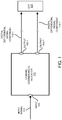
- the dynamic common mode adjustor 140 includes: an input 105 (such as a port, pin, etc.) that receives an input signal 115 (such as signal x).
- the dynamic common mode adjustor 140 further includes an output 108 (such as output 108-1 and output 108-2) that outputs an output signal 118 (such as signal y).
- the output signal 108 is a differential signal including digital differential signal component 118-1 (such as signal yp) and digital differential signal component 118-2 (such as signal yn).
- the dynamic common mode adjustor 140 i) derives differential signal 118 (differential signal y) from the received input signal, and ii) varies an offset of the differential signal 118 as a function of a magnitude or level of the received input signal 115.
- the dynamic common mode adjustor 140 outputs the offset differential signal 118 from the output 108. More specifically, the dynamic common mode adjustor 140 outputs digital differential signal component 118-1 (first signal such as yp) from output 108-1 to entity such as circuit 125; the dynamic common mode adjustor 140 outputs digital differential signal component 118-2 (second signal such as yn) from output 108-2 to entity such as circuit 125.
- digital differential signal component 118-1 first signal such as yp
- second signal such as yn
- the received input signal 115 is an analog or digital signal; the differential signal derived from the received input signal is an analog signal or digital signal.
- controlling an offset (such as common mode setting) associated with differential signal 118 provides increased system performance for parameters such as noise, distortion, and power consumption.
- FIG. 2 is an example diagram illustrating implementation of a dynamic common mode adjustor and digital-to-analog converter according to embodiments herein.
- the offset differential signal 118 outputted from the output 108 of dynamic common mode adjustor 140 includes first signal yp (such as digital differential signal component 118-1) and a second signal yn (such as digital differential signal component 118-2).
- the dynamic common mode adjustor 140 applies a generated offset (common mode adjustment value) to control a respective common mode setting of the output signal 118 (differential signal such as including digital differential signal component 118-1 and digital differential signal component 118-2) outputted downstream to the differential digital-to-analog converter 260.
- a generated offset common mode adjustment value
- the differential digital-to-analog converter 260 receives the differential signal 118 and converts it into the analog output signal 218 (such as analog voltage Vd).
- the output signal 218 is a differential analog signal comprising analog differential signal component 218-1 (signal yp) and analog differential signal component 218-2 (signal yn).
- analog differential signal component 218-1 signal yp
- analog differential signal component 218-2 signal yn
- the dynamic common mode adjustor 140 varies a magnitude of the differential signal Vd depending on a magnitude or level of the received input signal 115.
- certain embodiments herein include controlling a common mode setting of the differential output signal pair vp and vn (such as [vp + vn] / 2) as well as a magnitude of the differential output signal Vd depending on a magnitude of the input signal 115 (signal x) being converted.
- a magnitude of the voltage Vd (difference between voltage vp and voltage vn) is proportional to the input signal x (such as over a range of multiple input values of signal x). Additionally, or alternatively, the magnitude of the output voltage proportionally tracks a magnitude of the input signal 115.
- embodiments herein can be configured to include a digital-to-analog converter 260 that receives the offset differential signal 118 and generates, from it, a respective differential analog output voltage signal 218 (analog voltage Vd).
- differential output signal 218 can include any of multiple techniques.
- the dynamic common mode adjustor 140 includes or has access to adjustment information 250.
- Adjustment information 250 includes any suitable information enabling generation of an appropriate offset value (or common mode setting) to apply to the differential signals 118, 218.
- FIG. 3 is an example diagram illustrating implementation of a dynamic common mode adjustor and digital-to-analog converter according to embodiments herein.
- the differential digital-to-analog converter 260 includes two digital-to-analog converters (namely, digital-to-analog converter 260-1 and digital-to-analog converter 260-2).
- the first digital-to-analog converter 260-1 converts the first digital value 118-1 (such as signal yp) into a first analog output signal 218-1 (such as analog voltage or current vp); the second digital-to-analog converter 260-2 converts the second digital value 118-2 into a second analog output signal 218-2 (such as analog voltage or current vn).
- a magnitude and offset (common mode setting) of the respective differential analog output signal, Vd varies depending on a magnitude of the input signal 115, and on the adjustment information 250.
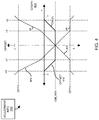
- FIG. 4 is an example graph illustrating variation of common mode settings depending on an input according to embodiments herein.
- graph 400 and corresponding functions 401, 402, and 410 represent an instantiation of the adjustment information 250 used to derive differential signal 118 and/or corresponding common mode adjustment settings from the input signal 115.
- the adjustment information 250 can be implemented via one or more piece-wise linear functions that provide different common mode adjustment settings over a range of different input or output values.
- the X-axis represents different possible values of the input signal 115; the Y-axis represents a value of a corresponding offset/output signal.
- Function 401 indicates one embodiment of mapping the input signal 115 (signal x) to a corresponding value of signal yp for a range of different input values; function 402 indicates an embodiment of mapping of the input signal 115 (signal x) to a corresponding value of signal yn for a range of different input values.
- attributes (slopes, number of linear pieces, offset, etc.) of functions 401 and 402 can be adjusted to accommodate any desirable common mode settings.
- the combination of signal yn and yp is a differential signal 118.
- Applications of function 401 to produce signal yn and application of function 402 to produce signal yp result in a corresponding differential signal 118 having a common mode setting as indicated by function CM (x) in graph 400.
- the common mode setting of the differential signal 118 and signal 218 is a fixed value - CM_MIN.
- the common mode setting of the differential signal 118 and 218 varies as shown with respect to the input voltage 115.
- the common mode setting of the differential signal 118 and signal 218 is substantially zero.
- the adjustment information 250 can be configured as map information that maps input values (associated with signal x) to different corresponding differential output values.
- the dynamic common mode adjustor 140 can be configured to derive the differential signal via mapping of the received input signal 115 (signal x) to a first value and second value specified by the mapping information.
- the input signal is 0.4.
- the difference between the signal vp and vn is 0.4 (two times the input signal of 0.2).
- the difference between the signal yp and vn is 0.8 (two times the input signal of 0.4).
- the first signal value and the second signal value generated by the dynamic common mode adjustor 140 via mapping represent settings of a pair of signals (such as yp and yn) representing the differential output signal 118.
- map information can include a piece-wise linear math function (as illustrated in graph 400) to derive the offset (common mode settings) associated with the differential signals 118, 218.
- the dynamic common mode adjustor 140 implements (via signal processing) one or more polynomial (mathematical) functions to produce the offset that is applied to a respective differential signal 118, 218 derived from the received input signal 115.
- FIG. 5 is an example diagram illustrating implementation of a dynamic common mode adjustor and a differential digital-to-analog converter according to embodiments herein.
- an instantiation of the dynamic common mode adjustor 140 can be configured to include summer 521, summer 522, sign inverter 550 (gain of-1), and adjustor 540.
- the adjustor 540 receives the input signal 115.
- the adjustor 540 outputs a respective common mode adjustment signal 535 [having a value of CM(x)] to both summer 521 and summer 522.
- Sign inverter 550 applies a gain of -1 to the input signal 115 to produce signal 515 (-x).
- the dynamic common mode adjustor 140 modifies the common mode setting associated with the differential signals 118 and 218 depending on a magnitude of the input signal 115.
- the adjustment signal 535 (or offset 410) is constant (such as -CM MIN) for magnitudes of signal 115 between -x1 and x1; adjustment signal 535 (or offset 410) varies for magnitudes of signal 115 between -x2 and -x1 and between x1 and x2; adjustment signal 535 (or offset 410) is set to zero for values of signal 115 less than -x2 and greater than x2.
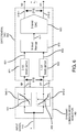
- FIG. 6 is an example diagram illustrating implementation of a dynamic common mode adjustor and a differential digital-to-analog converter according to embodiments herein.
- the dynamic common mode adjustor 140 includes adjustor 640-1 and adjustor 640-2.
- the adjustor 640-1 implements function 401 to convert the input signal 115 to digital differential signal component 118-1; the adjustor 640-2 implements function 402 to convert the input signal 115 to digital differential signal component 118-2.
- differential digital-to-analog converter 660 receives the differential signal 118 and converts it into respective analog differential signal 218.
- the differential digital-to-analog converter 660 includes modulator 621, modulator 622, remapper 670, and 3-level digital-to-analog converter 680.
- the modulator 621 receives digital differential signal component 118-1 and converts it into signal 631 (such as a serial stream representing the digital differential signal component 118-1).
- the modulator 622 receives digital differential signal component 118-2 and converts it into signal 632 (such as a serial stream representing the digital differential signal component 118-2).
- the remapper 670 converts a combination of the received signals 631 and 632 into signal 671 representative of the differential signal.
- digital-to-analog converter 680 converts the signal 671 into the differential signal 218.
- functions 401 and 402 implemented by the adjustors 640-1 and 640-2 provide different common mode adjustments depending on a magnitude of the input signal 115. Note again that the functions 401 and 402 can be adjusted to accommodate any desirable common mode settings.
- FIG. 7 is an example block diagram of a computer device for implementing any of the operations as discussed herein according to embodiments herein.
- computer system 700 (such as implemented by any of one or more resources such as dynamic common mode adjustor 140, digital-to-analog converters, etc.) of the present example includes an interconnect 711 that couples computer readable storage media 712 such as a non-transitory type of media (or hardware storage media) in which digital information can be stored and retrieved, a processor 713 (e.g., computer processor hardware such as one or more processor devices), I/O interface 714, and a communications interface 717.
- computer readable storage media 712 such as a non-transitory type of media (or hardware storage media) in which digital information can be stored and retrieved
- processor 713 e.g., computer processor hardware such as one or more processor devices
- I/O interface 714 provides connectivity to any suitable resources such as a respective resource storing adjustment information 250.
- adjustment information 250 facilitates generation of an offset value (common mode setting) applied to the respective differential signal 118 depending on a level or setting of the input signal 115.
- Computer readable storage medium 712 can be any hardware storage resource or device such as memory, optical storage, hard drive, floppy disk, etc. In one embodiment, the computer readable storage medium 712 stores instructions and/or data used by the dynamic common mode adjustor application 140-1 to perform any of the operations as described herein.
- communications interface 717 enables the computer system 700 and processor 713 to communicate over a resource such as network 190 to retrieve information from remote sources and communicate with other computers.
- Dynamic common mode adjustor application 140-1 can be configured to include instructions to implement any of the operations as discussed herein.
- processor 713 accesses computer readable storage media 712 via the use of interconnect 711 in order to launch, run, execute, interpret or otherwise perform the instructions in dynamic common mode adjustor application 140-1 stored on computer readable storage medium 712.
- Execution of the dynamic common mode adjustor application 140-1 produces processing functionality such as control process 140-2 in processor 713.
- the dynamic common mode adjustor process 140-2 associated with processor 713 represents one or more aspects of executing dynamic common mode adjustor application 140-1 within or upon the processor 713 in the computer system 700.
- computer system 700 can be a micro-controller device, logic, hardware processor, hybrid analog/digital circuitry, etc., configured to perform any of the operations as described herein.
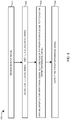
- FIG. 8 is an example diagram illustrating a method according to embodiments herein.
- the dynamic common mode adjustor 140 receives an input signal 115 (signal x).
- the dynamic common mode adjustor 140 derives a differential signal 118 (combination of signal 118-1 and signal 118-2) from the received input signal 115.
- the dynamic common mode adjustor 140 varies an offset of the differential signal 118 as a function of the received input signal 115 to produce offset differential signal 118.
- the dynamic common mode adjustor 140 outputs the offset differential signal 118.
- Example 1 An apparatus comprising: an input operable to receive an input signal; a dynamic common mode adjustor operable to: i) derive a differential signal from the received input signal, and ii) vary a common mode setting of the differential signal as a function of the received input signal to produce an offset differential signal; and an output operable to output the offset differential signal.
- Example 2 The apparatus as in example 1, wherein the dynamic common mode adjustor varies the differential signal depending on the received input signal.
- Example 3 The apparatus as in example 1, wherein the received input signal is a digital signal; and wherein the differential signal derived from the received input signal is an analog signal.
- Example 4 The apparatus as in example 1 further comprising: map information, the map information providing a mapping of input values to corresponding differential output values; and wherein the dynamic common mode adjustor derives the differential signal via mapping of the received input signal to a first value and second value specified by the mapping information.
- Example 5 The apparatus as in example 1, wherein the dynamic common mode adjustor applies a piece-wise linear math function to derive the offset differential signal from the received input signal.
- Example 6 The apparatus as in example 1, wherein the dynamic common mode adjustor is operable to implement one or more polynomial math functions to derive the offset differential signal from the received input signal.
- Example 7 The apparatus as in example 1, wherein the received input signal is a digital signal; and wherein the offset differential signal outputted from the output includes a first signal and a second signal, a difference between the second signal and the first signal proportionally varying with respect to the received input signal.
- Example 8 The apparatus as in example 1 further comprising: a digital-to-analog converter operable to receive the offset differential signal and generate a respective differential analog output signal.
- Example 9 The apparatus as in example 8, wherein the offset differential signal is a pair of signals including a first digital value and a second digital value; wherein the digital-to-analog converter includes a first digital-to-analog converter and a second digital-to-analog converter, the first digital-to-analog converter operable to convert the first digital value into a first analog output voltage, the second digital-to-analog converter operable to convert the second digital value into a second analog output voltage; and wherein the respective differential analog output signal includes the first analog output voltage and the second analog output voltage.
- the digital-to-analog converter includes a first digital-to-analog converter and a second digital-to-analog converter, the first digital-to-analog converter operable to convert the first digital value into a first analog output voltage, the second digital-to-analog converter operable to convert the second digital value into a second analog output voltage; and wherein the respective differential analog output signal includes the first analog output voltage and the second analog output voltage.
- Example 10 The apparatus as in example 1, wherein the dynamic common mode adjustor includes an offset adjustor operable to generate the offset; and wherein the offset adjustor generates the common mode setting as a fixed value during operating conditions in which the received input signal falls within a first range; and wherein the offset adjustor varies the common mode setting during operating conditions in which the received input signal falls within a second range.
- the dynamic common mode adjustor includes an offset adjustor operable to generate the offset; and wherein the offset adjustor generates the common mode setting as a fixed value during operating conditions in which the received input signal falls within a first range; and wherein the offset adjustor varies the common mode setting during operating conditions in which the received input signal falls within a second range.
- Example 11 The apparatus as in example 1, wherein the differential signal includes a first signal and a second signal derived from the input signal; wherein the common mode setting is an offset; and wherein the dynamic common mode adjustor is operable to apply the offset to both the first signal and the second signal, a difference between the first signal and the second signal being proportional to the received input signal.
- Example 12 A method comprising: receiving an input signal; deriving a differential signal from the received input signal; varying an offset of the differential signal as a function of the received input signal to produce an offset differential signal; and outputting the offset differential signal.
- Example 13 The method as in example 12 further comprising: proportionally varying the differential signal depending on the magnitude of the received input signal.
- Example 14 The method as in example 12, wherein the received input signal is a digital signal; and wherein the offset differential signal derived from the received input signal is an analog signal.
- Example 15 The method as in example 12, wherein deriving the offset differential signal from the received input signal includes: via mapping information, mapping the received input signal to a first value and second value.
- Example 16 The method as in example 12 further comprising: implementing a piece-wise linear math function to derive the offset differential signal from the received input signal.
- Example 17 The method as in example 12 further comprising: implementing one or more polynomial math functions to derive the offset differential signal from the received input signal.
- Example 18 The method as in example 12, wherein the received input signal is a digital signal, the method further comprising: producing the differential signal to include a first signal and a second signal, a difference between the second signal and the first signal proportionally varying with respect to the received input signal.
- Example 19 The method as in example 12 further comprising: via a digital-to-analog converter, converting the differential signal into a respective differential analog output voltage signal.
- Example 20 The method as in example 19, wherein the differential signal is a pair of signals including a first digital value and a second digital value, the method further comprising: converting the first digital value into a first analog output voltage; converting the second digital value into a second analog output voltage, the respective differential analog output signal including the first analog output voltage and the second analog output voltage.
- Example 21 The method as in example 12 further comprising: generating a magnitude of the offset as a fixed value during operating conditions in which the received input signal falls within a first range; and varying the offset during operating conditions in which the received input signal falls within a second range.
- Example 22 The method as in example 12, wherein the differential signal includes a first signal and a second signal derived from the input signal, the method further comprising: applying the offset to both the first signal and the second signal, a difference between the first signal and second signal being proportional to the receive input signal.
- Example 23 Computer-readable storage hardware having instructions stored thereon, the instructions, when carried out by computer processor hardware, cause the computer processor hardware to: receive an input signal; derive a differential signal from the received input signal; vary an offset of the differential signal as a function of the received input signal to produce an offset differential signal; and output the offset differential signal.
- An algorithm as described herein, and generally, is considered to be a self-consistent sequence of operations or similar processing leading to a desired result.
- operations or processing involve physical manipulation of physical quantities.
- quantities may take the form of electrical or magnetic signals capable of being stored, transferred, combined, compared or otherwise manipulated. It has been convenient at times, principally for reasons of common usage, to refer to such signals as bits, data, values, elements, symbols, characters, terms, numbers, numerals or the like. It should be understood, however, that all of these and similar terms are to be associated with appropriate physical quantities and are merely convenient labels.
Landscapes
- Engineering & Computer Science (AREA)
- Theoretical Computer Science (AREA)
- Power Engineering (AREA)
- Amplifiers (AREA)
Abstract
Description
- A conventional differential DAC (Digital-to-Analog Converter) typically has a fixed common-mode DC voltage setting at its respective output. For example, a conventional differential digital-to-analog converter device can be configured to receive an input signal. The digital-to-analog converter produces an output voltage whose magnitude varies depending on the input signal.
- Typically, the common mode setting of the conventional digital-to-analog converter is selected to an appropriate fixed common mode DC value to optimize its full-scale output signal swing. Since the common-mode setting of a conventional digital-to-analog converter is constant or fixed, it typically does not provide peak performance at low level signals (i.e., signals that are fairly low in magnitude).
- This disclosure includes the observation that electronic circuitry (such as a digital-to-analog converter and/or corresponding circuitry) typically operates more efficiently when an output voltage is set to an appropriate common mode voltage. In certain instances, this means that a desirable common mode voltage may be different depending on a magnitude of the output voltage being generated.
- Embodiments herein include novel ways of providing improved circuit performance associated with a digital-to-analog converter and/or related circuitry. For example, one embodiment herein includes dynamically controlling a common-mode setting of a differential signal depending at least in part on a magnitude of an input signal from which the output signal is derived. Providing signal-dependent common-mode control as described herein increases system performance for parameters such as noise, distortion, and power consumption associated with a respective electronic circuit.
- More specifically, in one embodiment, an apparatus (such as an electronic circuit) providing improved system performance comprises: an input operable to receive an input signal; a dynamic common mode adjustor operable to: i) derive a differential signal from the received input signal, and ii) vary an offset of the differential signal as a function of a magnitude or level of the received input signal to produce an offset differential signal; and an output operable to output the offset differential signal. As previously discussed, controlling an offset (such as common mode setting) associated with a differential signal provides increased system performance for parameters such as noise, distortion, and power consumption of a corresponding electronic circuit.
- Typically, the dynamic common mode adjustor as described herein is instantiated as an electronic circuit such as associated with a digital-to-analog converter, amplifier, etc. However, the dynamic common mode adjustor can be implemented in any suitable manner depending on the embodiment.
- In further example embodiments, the offset differential signal outputted from the output includes a first signal component and a second signal component; the dynamic common mode adjustor is operable to apply the generated offset value (common mode adjustment) to both the first signal and the second signal to control a respective common mode setting.
- Yet further, a magnitude of a difference between the second signal and the first signal proportionally varies with respect to a magnitude of the received input signal. In other words, in one embodiment, the dynamic common mode adjustor varies a magnitude of the differential signal depending on a magnitude or level of the received input signal. Accordingly, certain embodiments herein include controlling a common mode setting of the differential output signal as well as a magnitude of the differential output signal depending on a magnitude or level of the input signal being converted.
- In one embodiment, the received input signal is a digital signal; the differential signal derived from the received input signal is an analog signal.
- Adjustment of the common mode setting or offset associated with a differential output signal can include any of multiple techniques. For example, in one embodiment, the dynamic common mode adjustor includes or has access to map information. The map information provides a mapping of input values to corresponding differential output values. During operation, the dynamic common mode adjustor derives the differential signal via mapping of a magnitude of the received input signal to a first value and second value specified by the mapping information. In one embodiment, the first value and the second value represent settings of a pair signals representing the differential output signal whose common mode setting is adjusted.
- In accordance with further embodiments, the dynamic common mode adjustor can be configured to apply a piece-wise linear math function to derive the offset (common mode settings) associated with the differential signal.
- In yet further embodiments, the dynamic common mode adjustor is operable to implement one or more polynomial (mathematical) functions to produce the offset that is applied to a respective differential signal derived from the received input signal.
- In accordance with further embodiments, in addition to a dynamic common mode adjustor, the electronic circuit as described herein can be configured to include a digital-to-analog converter circuit operable to receive the offset differential signal. The digital-to-analog converter generates a respective differential analog output signal (current or voltage signal) from the offset differential signal received from the dynamic common mode adjustor.
- Note further that the digital-to-analog converter circuit can be configured to include a first digital-to-analog converter and a second digital-to-analog converter. In such an instance, the first digital-to-analog converter converts the first digital value into a first analog output signal (voltage signal or current signal); the second digital-to-analog converter operable to convert the second digital value into a second analog output signal (voltage signal or current signal). The respective differential analog output signal includes the first analog output signal (such as voltage signal or current signal) and the second analog output signal (such as voltage signal or current signal).
- In yet further embodiments, the dynamic common mode adjustor includes an offset adjustor operable to generate the offset used to control a common mode setting associated with the differential signal. In one embodiment, the offset adjustor generates (or controls) a magnitude of the offset to be a fixed value during operating conditions in which the magnitude or level of the received input signal falls within a first magnitude range (such as when an absolute value of a magnitude of the input signal is less than threshold value). The offset adjustor can be configured to vary a magnitude or level of the offset during operating conditions in which the magnitude of the received input signal falls within a second magnitude range. Accordingly, the dynamic common mode adjustor can be configured to adjust the common mode setting of an output signal (such as voltage signal or current signal) to ensure further efficient processing of the output signal (voltage signal or current signal).
- These and other more specific embodiments are disclosed in more detail below.
- Note further that although embodiments as discussed herein are applicable to electronic circuits such as those implementing digital-to-analog converters, amplifiers, differential signal generators, etc., the concepts disclosed herein may be advantageously applied to any other suitable topologies as well as general power supply control applications.
- Additionally, note that embodiments herein can include computer processor hardware (that executes corresponding switch instructions) to carry out and/or support any or all of the method operations disclosed herein. In other words, one or more computerized devices or processors (computer processor hardware) can be programmed and/or configured to operate as explained herein to carry out different embodiments of the invention.
- Yet other embodiments herein include software programs to perform the steps and operations summarized above and disclosed in detail below. One such embodiment comprises a computer program product that has non-transitory computer-storage media (e.g., memory, disk, flash, ...) including computer program instructions and/or logic encoded thereon that, when performed in a computerized device having a processor and corresponding memory, programs the processor to perform any of the operations disclosed herein. Such arrangements are typically provided as software instructions, code, and/or other data (e.g., data structures) arranged or encoded on a computer readable storage medium or non-transitory computer readable media such as an optical medium (e.g., CD-ROM), floppy or hard disk or other a medium such as firmware or microcode in one or more ROM or RAM or PROM chips, an Application Specific Integrated Circuit (ASIC), circuit logic, etc. The software or firmware or other such configurations can be installed onto a respective controller circuit to cause the controller circuit (such as logic) to perform the techniques explained herein.
- Accordingly, one embodiment of the present disclosure is directed to a computer program product that includes a computer readable medium having instructions stored thereon for supporting operations such as controlling one or more phases in a power supply. For example, in one embodiment, the instructions, when carried out by computer processor hardware (one or more computer devices, control logic, digital circuitry, etc.), cause the computer processor hardware to: receive an input signal; derive a differential signal from the received input signal; control an offset of the differential signal as a function of the received input signal to produce an offset differential signal; and output the offset differential signal.
- The ordering of the operations as described herein has been added for clarity sake. The operations can be performed in any suitable order.
- It is to be understood that the system, method, device, apparatus, logic, etc., as discussed herein can be embodied strictly as hardware (such as analog circuitry, digital circuitry, logic, etc.), as a hybrid of software and hardware, or as software alone such as within a processor, or within an operating system or a within a software application.
- Note that although each of the different features, techniques, configurations, etc., herein may be discussed in different places of this disclosure, it is intended, where appropriate, that each of the concepts can optionally be executed independently of each other or in combination with each other. Accordingly, the one or more present inventions as described herein can be embodied and viewed in many different ways.
- Also, note that this preliminary discussion of embodiments herein purposefully does not specify every embodiment and/or incrementally novel aspect of the present disclosure or claimed invention(s). Instead, this brief description only presents general embodiments and corresponding points of novelty over conventional techniques. For additional details and/or possible perspectives (permutations) of the invention(s), the reader is directed to the Detailed Description section and corresponding figures of the present disclosure as further discussed below.
-
FIG. 1 is an example diagram illustrating a dynamic common mode adjustor according to embodiments herein. -
FIG. 2 is an example diagram illustrating implementation of a dynamic common mode adjustor and digital-to-analog converter according to embodiments herein. -
FIG. 3 is an example diagram illustrating implementation of a dynamic common mode adjustor and digital-to-analog converter circuit according to embodiments herein. -
FIG. 4 is an example graph illustrating variation of common mode settings depending on an input according to embodiments herein. -
FIG. 5 is an example diagram illustrating implementation of a dynamic common mode adjustor and a differential digital-to-analog converter according to embodiments herein. -
FIG. 6 is an example diagram illustrating implementation of a dynamic common mode adjustor and a differential digital-to-analog converter according to embodiments herein. -
FIG. 7 is an example diagram illustrating computer processor hardware and related software instructions or logic circuit to execute methods according to embodiments herein. -
FIG. 8 is an example diagram illustrating a method according to embodiments herein. - The foregoing and other objects, features, and advantages of embodiments herein will be apparent from the following more particular description herein, as illustrated in the accompanying drawings in which like reference characters refer to the same parts throughout the different views. The drawings are not necessarily to scale, with emphasis instead being placed upon illustrating the embodiments, principles, concepts, etc.
- According to one embodiment, an apparatus such as an electronic circuit includes an input operable to receive an input signal; a dynamic common mode adjustor operable to: i) derive a differential signal from the received input signal, and ii) vary an offset of the differential signal as a function of a magnitude or level of the received input signal to produce an offset differential signal; and an output operable to output the offset differential signal. In one configuration, the offset differential signal outputted from the output includes a first signal and a second signal; a magnitude or amount of a difference between the second signal and the first signal proportionally varies with respect to a magnitude or level of the received input signal.
- Now, more specifically,
FIG. 1 is an example diagram illustrating general components of a multi-stage amplifier device according to conventional techniques. - As previously discussed, embodiments herein include novel ways of providing improved circuit performance associated with a digital-to-analog converter and/or related circuitry. For example, one embodiment herein includes dynamically controlling a common-mode setting of a differential DAC, depending on a magnitude of the input signal being converted into a respective analog signal (such as a differential output signal proportional to the input). Providing signal-dependent common-mode control as described herein provides increased system performance for parameters such as noise, distortion, and power consumption. In other words, dynamically modifying a common mode setting (or offset) associated with a generated signal (such as voltage or current signal) supports lower noise, lower distortion and lower power consumption.
- In this example embodiment, an apparatus (such as an electrical circuit, device, hardware, software, etc.) includes a dynamic
common mode adjustor 140. Typically, the dynamiccommon mode adjustor 140 as described herein is instantiated as an electronic circuit such as associated with a digital-to-analog converter, amplifier, etc. However, the dynamiccommon mode adjustor 140 can be implemented in any suitable manner depending on the embodiment. - Further in this example embodiment, the dynamic
common mode adjustor 140 includes: an input 105 (such as a port, pin, etc.) that receives an input signal 115 (such as signal x). The dynamiccommon mode adjustor 140 further includes an output 108 (such as output 108-1 and output 108-2) that outputs an output signal 118 (such as signal y). - In one embodiment, the output signal 108 is a differential signal including digital differential signal component 118-1 (such as signal yp) and digital differential signal component 118-2 (such as signal yn).
- During operation, as previously discussed, the dynamic common mode adjustor 140: i) derives differential signal 118 (differential signal y) from the received input signal, and ii) varies an offset of the
differential signal 118 as a function of a magnitude or level of the receivedinput signal 115. - For example, the dynamic
common mode adjustor 140 outputs the offsetdifferential signal 118 from the output 108. More specifically, the dynamiccommon mode adjustor 140 outputs digital differential signal component 118-1 (first signal such as yp) from output 108-1 to entity such ascircuit 125; the dynamiccommon mode adjustor 140 outputs digital differential signal component 118-2 (second signal such as yn) from output 108-2 to entity such ascircuit 125. - In accordance with further embodiments, the received
input signal 115 is an analog or digital signal; the differential signal derived from the received input signal is an analog signal or digital signal. - As previously discussed, controlling an offset (such as common mode setting) associated with
differential signal 118 provides increased system performance for parameters such as noise, distortion, and power consumption. -
FIG. 2 is an example diagram illustrating implementation of a dynamic common mode adjustor and digital-to-analog converter according to embodiments herein. As shown in this example embodiment, the offsetdifferential signal 118 outputted from the output 108 of dynamiccommon mode adjustor 140 includes first signal yp (such as digital differential signal component 118-1) and a second signal yn (such as digital differential signal component 118-2). - As previously discussed, the dynamic
common mode adjustor 140 applies a generated offset (common mode adjustment value) to control a respective common mode setting of the output signal 118 (differential signal such as including digital differential signal component 118-1 and digital differential signal component 118-2) outputted downstream to the differential digital-to-analog converter 260. - As further shown, the differential digital-to-
analog converter 260 receives thedifferential signal 118 and converts it into the analog output signal 218 (such as analog voltage Vd). - In one embodiment, the
output signal 218 is a differential analog signal comprising analog differential signal component 218-1 (signal yp) and analog differential signal component 218-2 (signal yn). In such an instance, via the differential digital-to-analog converter 260, the digital differential signal component 118-1 (yp) is converted into corresponding equivalent analog voltage or current signal vp (such as differential signal component 218-1); via the differential digital-to-analog converter 260, the digital differential signal component 118-2 (yn) is converted into corresponding equivalent analog voltage or current signal vn (such as differential signal component 218-2). - Yet further, as previously discussed, a difference between the values yp and yn (as well as vp and vn) proportionally varies with respect to a level of the received
input signal 115. In other words, in one embodiment, the dynamiccommon mode adjustor 140 varies a magnitude of the differential signal Vd depending on a magnitude or level of the receivedinput signal 115. - Accordingly, certain embodiments herein include controlling a common mode setting of the differential output signal pair vp and vn (such as [vp + vn] / 2) as well as a magnitude of the differential output signal Vd depending on a magnitude of the input signal 115 (signal x) being converted.
- In one embodiment, a magnitude of the voltage Vd (difference between voltage vp and voltage vn) is proportional to the input signal x (such as over a range of multiple input values of signal x). Additionally, or alternatively, the magnitude of the output voltage proportionally tracks a magnitude of the
input signal 115. - Accordingly, in addition to a dynamic
common mode adjustor 140, embodiments herein can be configured to include a digital-to-analog converter 260 that receives the offsetdifferential signal 118 and generates, from it, a respective differential analog output voltage signal 218 (analog voltage Vd). - Note that adjustment of the common mode setting or offset associated with the
differential output signal 118 and thusdifferential output signal 218 can include any of multiple techniques. - For example, in one embodiment, the dynamic
common mode adjustor 140 includes or has access toadjustment information 250.Adjustment information 250 includes any suitable information enabling generation of an appropriate offset value (or common mode setting) to apply to thedifferential signals -
FIG. 3 is an example diagram illustrating implementation of a dynamic common mode adjustor and digital-to-analog converter according to embodiments herein. In this example embodiment, the differential digital-to-analog converter 260 includes two digital-to-analog converters (namely, digital-to-analog converter 260-1 and digital-to-analog converter 260-2). - During operation, the first digital-to-analog converter 260-1 converts the first digital value 118-1 (such as signal yp) into a first analog output signal 218-1 (such as analog voltage or current vp); the second digital-to-analog converter 260-2 converts the second digital value 118-2 into a second analog output signal 218-2 (such as analog voltage or current vn).
- In a similar manner as previously discussed, a magnitude and offset (common mode setting) of the respective differential analog output signal, Vd, varies depending on a magnitude of the
input signal 115, and on theadjustment information 250. -
FIG. 4 is an example graph illustrating variation of common mode settings depending on an input according to embodiments herein. In one embodiment,graph 400 andcorresponding functions adjustment information 250 used to derivedifferential signal 118 and/or corresponding common mode adjustment settings from theinput signal 115. As further shown, theadjustment information 250 can be implemented via one or more piece-wise linear functions that provide different common mode adjustment settings over a range of different input or output values. - More specifically, in this example embodiment, the X-axis represents different possible values of the
input signal 115; the Y-axis represents a value of a corresponding offset/output signal. -
Function 401 indicates one embodiment of mapping the input signal 115 (signal x) to a corresponding value of signal yp for a range of different input values; function 402 indicates an embodiment of mapping of the input signal 115 (signal x) to a corresponding value of signal yn for a range of different input values. - Note that attributes (slopes, number of linear pieces, offset, etc.) of
functions - As previously discussed, in accordance with further embodiments, the combination of signal yn and yp is a
differential signal 118. Applications offunction 401 to produce signal yn and application offunction 402 to produce signal yp result in a correspondingdifferential signal 118 having a common mode setting as indicated by function CM (x) ingraph 400. - When the
input signal 115 falls within a first range between -x1 and x1 (such as when an absolute value of the input signal is less than threshold value x1), the common mode setting of thedifferential signal 118 and signal 218 is a fixed value - CM_MIN. - When the
input signal 115 falls between a first range between -x2 and - x1 or between range x1 and x2, the common mode setting of thedifferential signal input voltage 115. - When the received
input signal 115 is less than -x2 or greater than x2 (such as when an absolute value of the input signal is greater than threshold value x2), the common mode setting of thedifferential signal 118 and signal 218 is substantially zero. - As previously discussed, the
adjustment information 250 can be configured as map information that maps input values (associated with signal x) to different corresponding differential output values. For example, during operation, the dynamiccommon mode adjustor 140 can be configured to derive the differential signal via mapping of the received input signal 115 (signal x) to a first value and second value specified by the mapping information. As a more specific example, assume that the input signal is 0.4. In such an instance, the dynamiccommon mode adjustor 140 uses adjustment information to map the value 0.2 to -0.2 (signal vp = -0.2) and -0.6 (signal vn = -0.6), in which the common mode or offset is -0.4. The difference between the signal vp and vn is 0.4 (two times the input signal of 0.2). In continuation of same example, assume the input signal is changed to be 0.4. The dynamiccommon mode adjustor 140 uses the adjustment information to map the value 0.4 to -0.0 (signal yp = - 0.0) and -0.8 (signal vn = -0.8), in which the common mode or offset is still -0.4. The difference between the signal yp and vn is 0.8 (two times the input signal of 0.4). - Example mapping is further discussed below.
- In one embodiment, the first signal value and the second signal value generated by the dynamic
common mode adjustor 140 via mapping represent settings of a pair of signals (such as yp and yn) representing thedifferential output signal 118. - Note that map information (such as a look-up table, etc.) can include a piece-wise linear math function (as illustrated in graph 400) to derive the offset (common mode settings) associated with the
differential signals - In yet further embodiments, the dynamic
common mode adjustor 140 implements (via signal processing) one or more polynomial (mathematical) functions to produce the offset that is applied to a respectivedifferential signal input signal 115. -
FIG. 5 is an example diagram illustrating implementation of a dynamic common mode adjustor and a differential digital-to-analog converter according to embodiments herein. - As shown in
FIG. 5 , an instantiation of the dynamiccommon mode adjustor 140 can be configured to includesummer 521,summer 522, sign inverter 550 (gain of-1), andadjustor 540. In such an embodiment, during operation, theadjustor 540 receives theinput signal 115. Viafunction 410, theadjustor 540 outputs a respective common mode adjustment signal 535 [having a value of CM(x)] to bothsummer 521 andsummer 522.Sign inverter 550 applies a gain of -1 to theinput signal 115 to produce signal 515 (-x). - As its name suggests,
summer 521 adds the commonmode adjustment signal 535 and theinput signal 115 to produce the digital differential signal component 118-1 (signal yp, where yp = x + CM (x)).Summer 522 adds the commonmode adjustment signal 535 and the inverted input signal 515 (-x) to produce the digital differential signal component 118-2 (signal yn, where yn = -x + CM (x)). - Accordingly, the dynamic
common mode adjustor 140 modifies the common mode setting associated with thedifferential signals input signal 115. - As previously discussed, the adjustment signal 535 (or offset 410) is constant (such as -CM MIN) for magnitudes of
signal 115 between -x1 and x1; adjustment signal 535 (or offset 410) varies for magnitudes ofsignal 115 between -x2 and -x1 and between x1 and x2; adjustment signal 535 (or offset 410) is set to zero for values ofsignal 115 less than -x2 and greater than x2. -
FIG. 6 is an example diagram illustrating implementation of a dynamic common mode adjustor and a differential digital-to-analog converter according to embodiments herein. In this example embodiment, the dynamiccommon mode adjustor 140 includes adjustor 640-1 and adjustor 640-2. - In this instance of the dynamic
common mode adjustor 140, the adjustor 640-1 implements function 401 to convert theinput signal 115 to digital differential signal component 118-1; the adjustor 640-2 implements function 402 to convert theinput signal 115 to digital differential signal component 118-2. - As further shown, differential digital-to-
analog converter 660 receives thedifferential signal 118 and converts it into respective analogdifferential signal 218. For example, in one embodiment, the differential digital-to-analog converter 660 includesmodulator 621,modulator 622,remapper 670, and 3-level digital-to-analog converter 680. - Further, during operation, the
modulator 621 receives digital differential signal component 118-1 and converts it into signal 631 (such as a serial stream representing the digital differential signal component 118-1). - The
modulator 622 receives digital differential signal component 118-2 and converts it into signal 632 (such as a serial stream representing the digital differential signal component 118-2). - As further shown, and as its name suggests, the
remapper 670 converts a combination of the receivedsignals signal 671 representative of the differential signal. Finally, digital-to-analog converter 680 converts thesignal 671 into thedifferential signal 218. - Thus, functions 401 and 402 implemented by the adjustors 640-1 and 640-2 provide different common mode adjustments depending on a magnitude of the
input signal 115. Note again that thefunctions -
FIG. 7 is an example block diagram of a computer device for implementing any of the operations as discussed herein according to embodiments herein. As shown, computer system 700 (such as implemented by any of one or more resources such as dynamiccommon mode adjustor 140, digital-to-analog converters, etc.) of the present example includes aninterconnect 711 that couples computerreadable storage media 712 such as a non-transitory type of media (or hardware storage media) in which digital information can be stored and retrieved, a processor 713 (e.g., computer processor hardware such as one or more processor devices), I/O interface 714, and acommunications interface 717. - I/
O interface 714 provides connectivity to any suitable resources such as a respective resource storingadjustment information 250. As previously discussed,adjustment information 250 facilitates generation of an offset value (common mode setting) applied to the respectivedifferential signal 118 depending on a level or setting of theinput signal 115. - Computer
readable storage medium 712 can be any hardware storage resource or device such as memory, optical storage, hard drive, floppy disk, etc. In one embodiment, the computerreadable storage medium 712 stores instructions and/or data used by the dynamic common mode adjustor application 140-1 to perform any of the operations as described herein. - Further in this example embodiment,
communications interface 717 enables thecomputer system 700 andprocessor 713 to communicate over a resource such asnetwork 190 to retrieve information from remote sources and communicate with other computers. - As shown, computer
readable storage media 712 is encoded with dynamic common mode adjustor application 140-1 (e.g., software, firmware, etc.) executed byprocessor 713. Dynamic common mode adjustor application 140-1 can be configured to include instructions to implement any of the operations as discussed herein. - During operation of one embodiment,
processor 713 accesses computerreadable storage media 712 via the use ofinterconnect 711 in order to launch, run, execute, interpret or otherwise perform the instructions in dynamic common mode adjustor application 140-1 stored on computerreadable storage medium 712. - Execution of the dynamic common mode adjustor application 140-1 produces processing functionality such as control process 140-2 in
processor 713. In other words, the dynamic common mode adjustor process 140-2 associated withprocessor 713 represents one or more aspects of executing dynamic common mode adjustor application 140-1 within or upon theprocessor 713 in thecomputer system 700. - In accordance with different embodiments, note that
computer system 700 can be a micro-controller device, logic, hardware processor, hybrid analog/digital circuitry, etc., configured to perform any of the operations as described herein. - Functionality supported by the different resources will now be discussed via flowchart in
FIG. 8 . Note that the steps in the flowcharts below can be executed in any suitable order. -
FIG. 8 is an example diagram illustrating a method according to embodiments herein. Inprocessing operation 810, the dynamiccommon mode adjustor 140 receives an input signal 115 (signal x). - In
processing operation 820, the dynamiccommon mode adjustor 140 derives a differential signal 118 (combination of signal 118-1 and signal 118-2) from the receivedinput signal 115. - In
processing operation 830, the dynamiccommon mode adjustor 140 varies an offset of thedifferential signal 118 as a function of the receivedinput signal 115 to produce offsetdifferential signal 118. - In
processing operation 840, the dynamiccommon mode adjustor 140 outputs the offsetdifferential signal 118. - Although the present disclosure is not so limited, the following numbered examples demonstrate one or more aspects of the disclosure.
- Example 1. An apparatus comprising: an input operable to receive an input signal; a dynamic common mode adjustor operable to: i) derive a differential signal from the received input signal, and ii) vary a common mode setting of the differential signal as a function of the received input signal to produce an offset differential signal; and an output operable to output the offset differential signal.
- Example 2. The apparatus as in example 1, wherein the dynamic common mode adjustor varies the differential signal depending on the received input signal.
- Example 3. The apparatus as in example 1, wherein the received input signal is a digital signal; and wherein the differential signal derived from the received input signal is an analog signal.
- Example 4. The apparatus as in example 1 further comprising: map information, the map information providing a mapping of input values to corresponding differential output values; and wherein the dynamic common mode adjustor derives the differential signal via mapping of the received input signal to a first value and second value specified by the mapping information.
- Example 5. The apparatus as in example 1, wherein the dynamic common mode adjustor applies a piece-wise linear math function to derive the offset differential signal from the received input signal.
- Example 6. The apparatus as in example 1, wherein the dynamic common mode adjustor is operable to implement one or more polynomial math functions to derive the offset differential signal from the received input signal.
- Example 7. The apparatus as in example 1, wherein the received input signal is a digital signal; and wherein the offset differential signal outputted from the output includes a first signal and a second signal, a difference between the second signal and the first signal proportionally varying with respect to the received input signal.
- Example 8. The apparatus as in example 1 further comprising: a digital-to-analog converter operable to receive the offset differential signal and generate a respective differential analog output signal.
- Example 9. The apparatus as in example 8, wherein the offset differential signal is a pair of signals including a first digital value and a second digital value; wherein the digital-to-analog converter includes a first digital-to-analog converter and a second digital-to-analog converter, the first digital-to-analog converter operable to convert the first digital value into a first analog output voltage, the second digital-to-analog converter operable to convert the second digital value into a second analog output voltage; and wherein the respective differential analog output signal includes the first analog output voltage and the second analog output voltage.
- Example 10. The apparatus as in example 1, wherein the dynamic common mode adjustor includes an offset adjustor operable to generate the offset; and wherein the offset adjustor generates the common mode setting as a fixed value during operating conditions in which the received input signal falls within a first range; and wherein the offset adjustor varies the common mode setting during operating conditions in which the received input signal falls within a second range.
- Example 11. The apparatus as in example 1, wherein the differential signal includes a first signal and a second signal derived from the input signal; wherein the common mode setting is an offset; and wherein the dynamic common mode adjustor is operable to apply the offset to both the first signal and the second signal, a difference between the first signal and the second signal being proportional to the received input signal.
- Example 12. A method comprising: receiving an input signal; deriving a differential signal from the received input signal; varying an offset of the differential signal as a function of the received input signal to produce an offset differential signal; and outputting the offset differential signal.
- Example 13. The method as in example 12 further comprising: proportionally varying the differential signal depending on the magnitude of the received input signal.
- Example 14. The method as in example 12, wherein the received input signal is a digital signal; and wherein the offset differential signal derived from the received input signal is an analog signal.
- Example 15. The method as in example 12, wherein deriving the offset differential signal from the received input signal includes: via mapping information, mapping the received input signal to a first value and second value.
- Example 16. The method as in example 12 further comprising: implementing a piece-wise linear math function to derive the offset differential signal from the received input signal.
- Example 17. The method as in example 12 further comprising: implementing one or more polynomial math functions to derive the offset differential signal from the received input signal.
- Example 18. The method as in example 12, wherein the received input signal is a digital signal, the method further comprising: producing the differential signal to include a first signal and a second signal, a difference between the second signal and the first signal proportionally varying with respect to the received input signal.
- Example 19. The method as in example 12 further comprising: via a digital-to-analog converter, converting the differential signal into a respective differential analog output voltage signal.
- Example 20. The method as in example 19, wherein the differential signal is a pair of signals including a first digital value and a second digital value, the method further comprising: converting the first digital value into a first analog output voltage; converting the second digital value into a second analog output voltage, the respective differential analog output signal including the first analog output voltage and the second analog output voltage.
- Example 21. The method as in example 12 further comprising: generating a magnitude of the offset as a fixed value during operating conditions in which the received input signal falls within a first range; and varying the offset during operating conditions in which the received input signal falls within a second range.
- Example 22. The method as in example 12, wherein the differential signal includes a first signal and a second signal derived from the input signal, the method further comprising: applying the offset to both the first signal and the second signal, a difference between the first signal and second signal being proportional to the receive input signal.
- Example 23. Computer-readable storage hardware having instructions stored thereon, the instructions, when carried out by computer processor hardware, cause the computer processor hardware to: receive an input signal; derive a differential signal from the received input signal; vary an offset of the differential signal as a function of the received input signal to produce an offset differential signal; and output the offset differential signal.
- Note again that techniques herein are well suited for use in differential signal generators, digital-to-analog converters, electronic circuits, etc. However, it should be noted that embodiments herein are not limited to use in such applications and that the techniques discussed herein are well suited for other applications as well.
- Based on the description set forth herein, numerous specific details have been set forth to provide a thorough understanding of claimed subject matter. However, it will be understood by those skilled in the art that claimed subject matter may be practiced without these specific details. In other instances, methods, apparatuses, systems, etc., that would be known by one of ordinary skill have not been described in detail so as not to obscure claimed subject matter. Some portions of the detailed description have been presented in terms of algorithms or symbolic representations of operations on data bits or binary digital signals stored within a computing system memory, such as a computer memory. These algorithmic descriptions or representations are examples of techniques used by those of ordinary skill in the data processing arts to convey the substance of their work to others skilled in the art. An algorithm as described herein, and generally, is considered to be a self-consistent sequence of operations or similar processing leading to a desired result. In this context, operations or processing involve physical manipulation of physical quantities. Typically, although not necessarily, such quantities may take the form of electrical or magnetic signals capable of being stored, transferred, combined, compared or otherwise manipulated. It has been convenient at times, principally for reasons of common usage, to refer to such signals as bits, data, values, elements, symbols, characters, terms, numbers, numerals or the like. It should be understood, however, that all of these and similar terms are to be associated with appropriate physical quantities and are merely convenient labels. Unless specifically stated otherwise, as apparent from the following discussion, it is appreciated that throughout this specification discussions utilizing terms such as "processing," "computing," "calculating," "determining" or the like refer to actions or processes of a computing platform, such as a computer or a similar electronic computing device, that manipulates or transforms data represented as physical electronic or magnetic quantities within memories, registers, or other information storage devices, transmission devices, or display devices of the computing platform.
Claims (15)
- An apparatus comprising:an input (105) operable to receive an input signal (115);a dynamic common mode adjustor (140) operable to: i) derive a differential signal from the received input signal (115), and ii) vary a common mode setting of the differential signal as a function of the received input signal (115) to produce an offset differential signal (118-1, 118-2); andan output (108-1, 108-2) operable to output the offset differential signal.
- The apparatus as in claim 1, wherein the dynamic common mode (140) adjustor varies the differential signal (118-1, 118-2) depending on the received input signal (115).
- The apparatus as in claim 1 or 2, wherein the received input signal (115) is a digital signal; and
wherein the differential signal (118-1, 118-2) derived from the received input signal (115) is an analog signal. - The apparatus as in any one of the preceding claims, further comprising:map information, the map information providing a mapping of input values to corresponding differential output values; andwherein the dynamic common mode adjustor (140) derives the differential signal (118-1, 118-2) via mapping of the received input signal (115) to a first value and second value specified by the mapping information.
- The apparatus as in any one of claims 1 to 4, wherein the dynamic common mode adjustor (140) applies a piece-wise linear math function to derive the offset differential signal (118-1, 118-2) from the received input signal (115).
- The apparatus as in any one of claims 1 to 4, wherein the dynamic common mode adjustor (140) is operable to implement one or more polynomial math functions to derive the offset differential signal (118-1, 118-2) from the received input signal (115).
- The apparatus as in any one of the preceding claims,, wherein the received input signal (115) is a digital signal; and
wherein the offset differential signal (118-1, 118-2) outputted from the output (108-1, 108-2) includes a first signal (118-1) and a second signal (118-2), a difference between the second signal (118-2) and the first signal (118-1) proportionally varying with respect to the received input signal (115). - The apparatus as in any one of the preceding claims, further comprising:
a digital-to-analog converter (260) operable to receive the offset differential signal (118-1, 118-2) and generate a respective differential analog output signal (218-1, 218-2). - The apparatus as in claim 8, wherein the offset differential signal (218-1, 218-2) is a pair of signals including a first digital value (118-1) and a second digital value (118-2);
wherein the digital-to-analog converter (260) includes a first digital-to-analog converter (260-1) and a second digital-to-analog converter (260-2), the first digital-to-analog converter (260-1) operable to convert the first digital value (118-1) into a first analog output voltage (218-1), the second digital-to-analog converter (260-2) operable to convert the second digital value (118-2) into a second analog output voltage (218-2); and
wherein the respective differential analog output signal (218-1, 218-2) includes the first analog output voltage (218-1) and the second analog output voltage (218-2). - The apparatus as in any one of the preceding claims, wherein the dynamic common mode adjustor (140) includes an offset adjustor (540) operable to generate the offset; and
wherein the offset adjustor (540) generates the common mode setting (535) as a fixed value during operating conditions in which the received input signal (115) falls within a first range; and
wherein the offset adjustor (140) varies the common mode setting (535) during operating conditions in which the received input signal (115) falls within a second range. - The apparatus as in claim 1, wherein the differential signal (118-1, 118-2) includes a first signal (118-1) and a second signal (118-2) derived from the input signal (115);
wherein the common mode setting (535) is an offset; and
wherein the dynamic common mode adjustor (140) is operable to apply the offset to both the first signal (118-1) and the second signal (118-2), a difference between the first signal (118-1) and the second signal (118-2) being proportional to the received input signal (115). - A method comprising:receiving an input signal (115);deriving a differential signal from the received input signal (115);varying an offset of the differential signal as a function of the received input signal (115) to produce an offset differential signal (118-1, 118-2); andoutputting the offset differential signal (118-1, 118-2).
- The method as in claim 12 further comprising:
proportionally varying the differential signal depending on the magnitude of the received input signal (115). - The method as in claim 12, wherein the received input signal (115) is a digital signal; and
wherein the offset differential signal (118-1, 118-2) derived from the received input signal (115) is an analog signal. - The method as in claim 12, wherein deriving the offset differential signal (118-1, 118-2) from the received input signal (115) includes:
via mapping information, mapping the received input signal (115) to a first value and second value.
Applications Claiming Priority (1)
| Application Number | Priority Date | Filing Date | Title |
|---|---|---|---|
| US16/458,897 US10735019B1 (en) | 2019-07-01 | 2019-07-01 | Dynamic common mode control |
Publications (2)
| Publication Number | Publication Date |
|---|---|
| EP3761512A1 true EP3761512A1 (en) | 2021-01-06 |
| EP3761512B1 EP3761512B1 (en) | 2025-06-18 |
Family
ID=71266429
Family Applications (1)
| Application Number | Title | Priority Date | Filing Date |
|---|---|---|---|
| EP20182769.8A Active EP3761512B1 (en) | 2019-07-01 | 2020-06-29 | Dynamic common mode control |
Country Status (4)
| Country | Link |
|---|---|
| US (2) | US10735019B1 (en) |
| EP (1) | EP3761512B1 (en) |
| KR (1) | KR102789674B1 (en) |
| CN (1) | CN112187268B (en) |
Families Citing this family (1)
| Publication number | Priority date | Publication date | Assignee | Title |
|---|---|---|---|---|
| US10735019B1 (en) * | 2019-07-01 | 2020-08-04 | Infineon Technologies Austria Ag | Dynamic common mode control |
Citations (1)
| Publication number | Priority date | Publication date | Assignee | Title |
|---|---|---|---|---|
| WO2002089332A1 (en) * | 2001-04-30 | 2002-11-07 | Telefonaktiebolaget Lm Ericsson (Publ) | A digital-to analog converter |
Family Cites Families (11)
| Publication number | Priority date | Publication date | Assignee | Title |
|---|---|---|---|---|
| JPH04357716A (en) * | 1991-06-04 | 1992-12-10 | Mitsubishi Electric Corp | Multi-channel d/a converter |
| US6433712B1 (en) * | 2001-07-25 | 2002-08-13 | Texas Instruments Incorporated | Offset error compensation of input signals in analog-to-digital converter |
| US8076973B2 (en) * | 2007-02-22 | 2011-12-13 | Intelleflex Corporation | Fully differential amplifier with continuous-time offset reduction |
| US7528752B1 (en) * | 2007-04-13 | 2009-05-05 | Link—A—Media Devices Corporation | Offset compensation scheme using a DAC |
| US8022851B2 (en) * | 2007-06-27 | 2011-09-20 | Nxp B.V. | DAC with data independent common mode dynamics |
| US7589591B2 (en) * | 2007-08-20 | 2009-09-15 | Semiconductor Components Industries, Llc | Differential sensing with high common mode rejection |
| EP2649729A4 (en) * | 2010-12-07 | 2017-03-15 | Marvell World Trade Ltd. | Digital to analog converter circuits and methods |
| US8633756B2 (en) * | 2011-07-21 | 2014-01-21 | National Semiconductor Corporation | Low voltage differential signaling (LVDS) circuitry and method for dynamically controlling common mode voltage at input |
| US9577522B2 (en) * | 2015-03-04 | 2017-02-21 | Infineon Technologies Americas Corp. | Pre-filtering in a power supply control circuit |
| US9692435B2 (en) * | 2015-04-16 | 2017-06-27 | Maxlinear, Inc. | Digital-to-analog converter (DAC) with digital offsets |
| US10735019B1 (en) * | 2019-07-01 | 2020-08-04 | Infineon Technologies Austria Ag | Dynamic common mode control |
-
2019
- 2019-07-01 US US16/458,897 patent/US10735019B1/en active Active
-
2020
- 2020-06-26 KR KR1020200078397A patent/KR102789674B1/en active Active
- 2020-06-29 EP EP20182769.8A patent/EP3761512B1/en active Active
- 2020-06-30 CN CN202010614943.9A patent/CN112187268B/en active Active
- 2020-07-14 US US16/928,244 patent/US11082057B2/en active Active
Patent Citations (1)
| Publication number | Priority date | Publication date | Assignee | Title |
|---|---|---|---|---|
| WO2002089332A1 (en) * | 2001-04-30 | 2002-11-07 | Telefonaktiebolaget Lm Ericsson (Publ) | A digital-to analog converter |
Non-Patent Citations (3)
| Title |
|---|
| ANONYMOUS: "Function (mathematics)", WIKIPEDIA, 26 June 2019 (2019-06-26), XP055751990, Retrieved from the Internet <URL:https://en.wikipedia.org/w/index.php?title=Function_(mathematics)&oldid=903550022> [retrieved on 20201118] * |
| ANONYMOUS: "Linear function", WIKIPEDIA, 14 April 2019 (2019-04-14), XP055751993, Retrieved from the Internet <URL:https://en.wikipedia.org/w/index.php?title=Linear_function&oldid=892400150> [retrieved on 20201118] * |
| OLA ANDERSSON ET AL: "A differential DAC architecture with variable common-mode level", PROC. 2002 IEEE INT. SYMP. ON CIRCUITS AND SYSTEMS, ISCAS'02, January 2002 (2002-01-01), pages I, XP055751920, Retrieved from the Internet <URL:https://ieeexplore.ieee.org/stampPDF/getPDF.jsp?tp=&arnumber=1009790&ref=aHR0cHM6Ly9pZWVleHBsb3JlLmllZWUub3JnL2RvY3VtZW50LzEwMDk3OTA=> [retrieved on 20201118] * |
Also Published As
| Publication number | Publication date |
|---|---|
| US20210006258A1 (en) | 2021-01-07 |
| CN112187268B (en) | 2026-03-10 |
| EP3761512B1 (en) | 2025-06-18 |
| KR20210003676A (en) | 2021-01-12 |
| US11082057B2 (en) | 2021-08-03 |
| US10735019B1 (en) | 2020-08-04 |
| CN112187268A (en) | 2021-01-05 |
| KR102789674B1 (en) | 2025-04-03 |
Similar Documents
| Publication | Publication Date | Title |
|---|---|---|
| JP5176692B2 (en) | Distortion compensation circuit and distortion compensation method | |
| US20040047432A1 (en) | Nonlinear distortion compensating circuit | |
| CN112311415B (en) | Electronic device and its wireless communication system | |
| CN101167243B (en) | Polar modulation circuit, integrated circuit, and radio apparatus | |
| CN109120265A (en) | A kind of bearing calibration of signal, device, chip and storage medium | |
| JP5109980B2 (en) | Power amplifier | |
| JP2003188656A (en) | Distortion compensation circuit | |
| JP4669513B2 (en) | Transmission circuit and communication device | |
| CN101841305B (en) | Power amplifying device and power amplifying method | |
| EP3761512B1 (en) | Dynamic common mode control | |
| US6924699B2 (en) | Apparatus, methods and articles of manufacture for digital modification in electromagnetic signal processing | |
| US5995546A (en) | Digital integrator for pulse-density modulation using an adder carry or an integrator overflow | |
| WO2010073889A1 (en) | Distortion compensation circuit, transmitter, and distortion compensation method | |
| JP2020035415A (en) | Power conversion device and control method for power conversion device | |
| JP4938597B2 (en) | Transmission circuit and communication device | |
| CN1985485B (en) | Amplitude modulation apparatus, amplitude limiting method, and computer readable program | |
| JP2007208684A (en) | Transmitter with distortion compensation function | |
| JP4707631B2 (en) | Polar modulation transmission apparatus and radio communication apparatus | |
| CN1366749A (en) | Multiplexing communication system and signal processing method thereof | |
| JPH0793538B2 (en) | Amplifier | |
| CN120301741B (en) | Signal transmitter and electronic equipment | |
| WO2005034461A1 (en) | Amplitude information extraction apparatus and amplitude information extraction method | |
| JPH0637837A (en) | Multi-level quadrature amplitude modulator | |
| CN101375493A (en) | polar modulation device | |
| JP2006352537A (en) | Digital modulator |
Legal Events
| Date | Code | Title | Description |
|---|---|---|---|
| PUAI | Public reference made under article 153(3) epc to a published international application that has entered the european phase |
Free format text: ORIGINAL CODE: 0009012 |
|
| STAA | Information on the status of an ep patent application or granted ep patent |
Free format text: STATUS: THE APPLICATION HAS BEEN PUBLISHED |
|
| AK | Designated contracting states |
Kind code of ref document: A1 Designated state(s): AL AT BE BG CH CY CZ DE DK EE ES FI FR GB GR HR HU IE IS IT LI LT LU LV MC MK MT NL NO PL PT RO RS SE SI SK SM TR |
|
| AX | Request for extension of the european patent |
Extension state: BA ME |
|
| STAA | Information on the status of an ep patent application or granted ep patent |
Free format text: STATUS: REQUEST FOR EXAMINATION WAS MADE |
|
| 17P | Request for examination filed |
Effective date: 20210706 |
|
| RBV | Designated contracting states (corrected) |
Designated state(s): AL AT BE BG CH CY CZ DE DK EE ES FI FR GB GR HR HU IE IS IT LI LT LU LV MC MK MT NL NO PL PT RO RS SE SI SK SM TR |
|
| STAA | Information on the status of an ep patent application or granted ep patent |
Free format text: STATUS: EXAMINATION IS IN PROGRESS |
|
| 17Q | First examination report despatched |
Effective date: 20220907 |
|
| GRAP | Despatch of communication of intention to grant a patent |
Free format text: ORIGINAL CODE: EPIDOSNIGR1 |
|
| STAA | Information on the status of an ep patent application or granted ep patent |
Free format text: STATUS: GRANT OF PATENT IS INTENDED |
|
| RIC1 | Information provided on ipc code assigned before grant |
Ipc: H03F 3/45 20060101ALN20241226BHEP Ipc: H03M 1/66 20060101ALN20241226BHEP Ipc: H03M 1/06 20060101AFI20241226BHEP |
|
| INTG | Intention to grant announced |
Effective date: 20250114 |
|
| RIC1 | Information provided on ipc code assigned before grant |
Ipc: H03F 3/45 20060101ALN20250106BHEP Ipc: H03M 1/66 20060101ALN20250106BHEP Ipc: H03M 1/06 20060101AFI20250106BHEP |
|
| GRAS | Grant fee paid |
Free format text: ORIGINAL CODE: EPIDOSNIGR3 |
|
| RAP1 | Party data changed (applicant data changed or rights of an application transferred) |
Owner name: CIRRUS LOGIC INTERNATIONAL SEMICONDUCTOR LTD. |
|
| GRAA | (expected) grant |
Free format text: ORIGINAL CODE: 0009210 |
|
| STAA | Information on the status of an ep patent application or granted ep patent |
Free format text: STATUS: THE PATENT HAS BEEN GRANTED |
|
| AK | Designated contracting states |
Kind code of ref document: B1 Designated state(s): AL AT BE BG CH CY CZ DE DK EE ES FI FR GB GR HR HU IE IS IT LI LT LU LV MC MK MT NL NO PL PT RO RS SE SI SK SM TR |
|
| REG | Reference to a national code |
Ref country code: GB Ref legal event code: FG4D |
|
| REG | Reference to a national code |
Ref country code: CH Ref legal event code: EP |
|
| REG | Reference to a national code |
Ref country code: DE Ref legal event code: R096 Ref document number: 602020052825 Country of ref document: DE |
|
| REG | Reference to a national code |
Ref country code: CH Ref legal event code: EP |
|
| REG | Reference to a national code |
Ref country code: IE Ref legal event code: FG4D |
|
| PG25 | Lapsed in a contracting state [announced via postgrant information from national office to epo] |
Ref country code: FI Free format text: LAPSE BECAUSE OF FAILURE TO SUBMIT A TRANSLATION OF THE DESCRIPTION OR TO PAY THE FEE WITHIN THE PRESCRIBED TIME-LIMIT Effective date: 20250618 |
|
| REG | Reference to a national code |
Ref country code: LT Ref legal event code: MG9D |
|
| PG25 | Lapsed in a contracting state [announced via postgrant information from national office to epo] |
Ref country code: NO Free format text: LAPSE BECAUSE OF FAILURE TO SUBMIT A TRANSLATION OF THE DESCRIPTION OR TO PAY THE FEE WITHIN THE PRESCRIBED TIME-LIMIT Effective date: 20250918 Ref country code: GR Free format text: LAPSE BECAUSE OF FAILURE TO SUBMIT A TRANSLATION OF THE DESCRIPTION OR TO PAY THE FEE WITHIN THE PRESCRIBED TIME-LIMIT Effective date: 20250919 |
|
| PG25 | Lapsed in a contracting state [announced via postgrant information from national office to epo] |
Ref country code: BG Free format text: LAPSE BECAUSE OF FAILURE TO SUBMIT A TRANSLATION OF THE DESCRIPTION OR TO PAY THE FEE WITHIN THE PRESCRIBED TIME-LIMIT Effective date: 20250618 |
|
| PG25 | Lapsed in a contracting state [announced via postgrant information from national office to epo] |
Ref country code: HR Free format text: LAPSE BECAUSE OF FAILURE TO SUBMIT A TRANSLATION OF THE DESCRIPTION OR TO PAY THE FEE WITHIN THE PRESCRIBED TIME-LIMIT Effective date: 20250618 |
|
| PG25 | Lapsed in a contracting state [announced via postgrant information from national office to epo] |
Ref country code: RS Free format text: LAPSE BECAUSE OF FAILURE TO SUBMIT A TRANSLATION OF THE DESCRIPTION OR TO PAY THE FEE WITHIN THE PRESCRIBED TIME-LIMIT Effective date: 20250918 |
|
| REG | Reference to a national code |
Ref country code: NL Ref legal event code: MP Effective date: 20250618 |
|
| PG25 | Lapsed in a contracting state [announced via postgrant information from national office to epo] |
Ref country code: LV Free format text: LAPSE BECAUSE OF FAILURE TO SUBMIT A TRANSLATION OF THE DESCRIPTION OR TO PAY THE FEE WITHIN THE PRESCRIBED TIME-LIMIT Effective date: 20250618 |
|
| PG25 | Lapsed in a contracting state [announced via postgrant information from national office to epo] |
Ref country code: NL Free format text: LAPSE BECAUSE OF FAILURE TO SUBMIT A TRANSLATION OF THE DESCRIPTION OR TO PAY THE FEE WITHIN THE PRESCRIBED TIME-LIMIT Effective date: 20250618 |
|
| PG25 | Lapsed in a contracting state [announced via postgrant information from national office to epo] |
Ref country code: PT Free format text: LAPSE BECAUSE OF FAILURE TO SUBMIT A TRANSLATION OF THE DESCRIPTION OR TO PAY THE FEE WITHIN THE PRESCRIBED TIME-LIMIT Effective date: 20251020 |
|
| REG | Reference to a national code |
Ref country code: AT Ref legal event code: MK05 Ref document number: 1805154 Country of ref document: AT Kind code of ref document: T Effective date: 20250618 |
|
| PG25 | Lapsed in a contracting state [announced via postgrant information from national office to epo] |
Ref country code: IS Free format text: LAPSE BECAUSE OF FAILURE TO SUBMIT A TRANSLATION OF THE DESCRIPTION OR TO PAY THE FEE WITHIN THE PRESCRIBED TIME-LIMIT Effective date: 20251018 |
|
| PG25 | Lapsed in a contracting state [announced via postgrant information from national office to epo] |
Ref country code: SM Free format text: LAPSE BECAUSE OF FAILURE TO SUBMIT A TRANSLATION OF THE DESCRIPTION OR TO PAY THE FEE WITHIN THE PRESCRIBED TIME-LIMIT Effective date: 20250618 Ref country code: AT Free format text: LAPSE BECAUSE OF FAILURE TO SUBMIT A TRANSLATION OF THE DESCRIPTION OR TO PAY THE FEE WITHIN THE PRESCRIBED TIME-LIMIT Effective date: 20250618 |
|
| PG25 | Lapsed in a contracting state [announced via postgrant information from national office to epo] |
Ref country code: CZ Free format text: LAPSE BECAUSE OF FAILURE TO SUBMIT A TRANSLATION OF THE DESCRIPTION OR TO PAY THE FEE WITHIN THE PRESCRIBED TIME-LIMIT Effective date: 20250618 |
|
| PG25 | Lapsed in a contracting state [announced via postgrant information from national office to epo] |
Ref country code: PL Free format text: LAPSE BECAUSE OF FAILURE TO SUBMIT A TRANSLATION OF THE DESCRIPTION OR TO PAY THE FEE WITHIN THE PRESCRIBED TIME-LIMIT Effective date: 20250618 |
|
| PG25 | Lapsed in a contracting state [announced via postgrant information from national office to epo] |
Ref country code: EE Free format text: LAPSE BECAUSE OF FAILURE TO SUBMIT A TRANSLATION OF THE DESCRIPTION OR TO PAY THE FEE WITHIN THE PRESCRIBED TIME-LIMIT Effective date: 20250618 |
|
| PG25 | Lapsed in a contracting state [announced via postgrant information from national office to epo] |
Ref country code: RO Free format text: LAPSE BECAUSE OF FAILURE TO SUBMIT A TRANSLATION OF THE DESCRIPTION OR TO PAY THE FEE WITHIN THE PRESCRIBED TIME-LIMIT Effective date: 20250618 Ref country code: SK Free format text: LAPSE BECAUSE OF FAILURE TO SUBMIT A TRANSLATION OF THE DESCRIPTION OR TO PAY THE FEE WITHIN THE PRESCRIBED TIME-LIMIT Effective date: 20250618 |
|
| REG | Reference to a national code |
Ref country code: CH Ref legal event code: H13 Free format text: ST27 STATUS EVENT CODE: U-0-0-H10-H13 (AS PROVIDED BY THE NATIONAL OFFICE) Effective date: 20260127 |
|
| PG25 | Lapsed in a contracting state [announced via postgrant information from national office to epo] |
Ref country code: ES Free format text: LAPSE BECAUSE OF FAILURE TO SUBMIT A TRANSLATION OF THE DESCRIPTION OR TO PAY THE FEE WITHIN THE PRESCRIBED TIME-LIMIT Effective date: 20250618 |
|
| PG25 | Lapsed in a contracting state [announced via postgrant information from national office to epo] |
Ref country code: LU Free format text: LAPSE BECAUSE OF NON-PAYMENT OF DUE FEES Effective date: 20250629 |
|
| REG | Reference to a national code |
Ref country code: BE Ref legal event code: MM Effective date: 20250630 |
|
| REG | Reference to a national code |
Ref country code: DE Ref legal event code: R097 Ref document number: 602020052825 Country of ref document: DE |
|
| PG25 | Lapsed in a contracting state [announced via postgrant information from national office to epo] |
Ref country code: MC Free format text: LAPSE BECAUSE OF FAILURE TO SUBMIT A TRANSLATION OF THE DESCRIPTION OR TO PAY THE FEE WITHIN THE PRESCRIBED TIME-LIMIT Effective date: 20250618 |
|
| PG25 | Lapsed in a contracting state [announced via postgrant information from national office to epo] |
Ref country code: IE Free format text: LAPSE BECAUSE OF NON-PAYMENT OF DUE FEES Effective date: 20250629 Ref country code: DK Free format text: LAPSE BECAUSE OF FAILURE TO SUBMIT A TRANSLATION OF THE DESCRIPTION OR TO PAY THE FEE WITHIN THE PRESCRIBED TIME-LIMIT Effective date: 20250618 |
|
| PG25 | Lapsed in a contracting state [announced via postgrant information from national office to epo] |
Ref country code: BE Free format text: LAPSE BECAUSE OF NON-PAYMENT OF DUE FEES Effective date: 20250630 Ref country code: IT Free format text: LAPSE BECAUSE OF FAILURE TO SUBMIT A TRANSLATION OF THE DESCRIPTION OR TO PAY THE FEE WITHIN THE PRESCRIBED TIME-LIMIT Effective date: 20250618 |
|
| PG25 | Lapsed in a contracting state [announced via postgrant information from national office to epo] |
Ref country code: CH Free format text: LAPSE BECAUSE OF NON-PAYMENT OF DUE FEES Effective date: 20250630 |
|
| PLBE | No opposition filed within time limit |
Free format text: ORIGINAL CODE: 0009261 |
|
| STAA | Information on the status of an ep patent application or granted ep patent |
Free format text: STATUS: NO OPPOSITION FILED WITHIN TIME LIMIT |
|
| REG | Reference to a national code |
Ref country code: CH Ref legal event code: L10 Free format text: ST27 STATUS EVENT CODE: U-0-0-L10-L00 (AS PROVIDED BY THE NATIONAL OFFICE) Effective date: 20260430 |
|
| 26N | No opposition filed |
Effective date: 20260319 |
|
| PG25 | Lapsed in a contracting state [announced via postgrant information from national office to epo] |
Ref country code: LT Free format text: LAPSE BECAUSE OF FAILURE TO SUBMIT A TRANSLATION OF THE DESCRIPTION OR TO PAY THE FEE WITHIN THE PRESCRIBED TIME-LIMIT Effective date: 20250618 |
|
| PGFP | Annual fee paid to national office [announced via postgrant information from national office to epo] |
Ref country code: GB Payment date: 20260629 Year of fee payment: 7 |
|
| PGFP | Annual fee paid to national office [announced via postgrant information from national office to epo] |
Ref country code: DE Payment date: 20260629 Year of fee payment: 7 |
|
| PG25 | Lapsed in a contracting state [announced via postgrant information from national office to epo] |
Ref country code: FR Free format text: LAPSE BECAUSE OF NON-PAYMENT OF DUE FEES Effective date: 20250818 |
|
| PG25 | Lapsed in a contracting state [announced via postgrant information from national office to epo] |
Ref country code: CY Free format text: LAPSE BECAUSE OF FAILURE TO SUBMIT A TRANSLATION OF THE DESCRIPTION OR TO PAY THE FEE WITHIN THE PRESCRIBED TIME-LIMIT Effective date: 20250618 Ref country code: SE Free format text: LAPSE BECAUSE OF FAILURE TO SUBMIT A TRANSLATION OF THE DESCRIPTION OR TO PAY THE FEE WITHIN THE PRESCRIBED TIME-LIMIT Effective date: 20250618 |