EP3761347A1 - Open web electrical support for contact pad and method of manufacture - Google Patents
Open web electrical support for contact pad and method of manufacture Download PDFInfo
- Publication number
- EP3761347A1 EP3761347A1 EP19425049.4A EP19425049A EP3761347A1 EP 3761347 A1 EP3761347 A1 EP 3761347A1 EP 19425049 A EP19425049 A EP 19425049A EP 3761347 A1 EP3761347 A1 EP 3761347A1
- Authority
- EP
- European Patent Office
- Prior art keywords
- support
- carbon
- cnts
- flexible section
- contact pad
- Prior art date
- Legal status (The legal status is an assumption and is not a legal conclusion. Google has not performed a legal analysis and makes no representation as to the accuracy of the status listed.)
- Granted
Links
Images



Classifications
-
- H—ELECTRICITY
- H10—SEMICONDUCTOR DEVICES; ELECTRIC SOLID-STATE DEVICES NOT OTHERWISE PROVIDED FOR
- H10W—GENERIC PACKAGES, INTERCONNECTIONS, CONNECTORS OR OTHER CONSTRUCTIONAL DETAILS OF DEVICES COVERED BY CLASS H10
- H10W70/00—Package substrates; Interposers; Redistribution layers [RDL]
- H10W70/60—Insulating or insulated package substrates; Interposers; Redistribution layers
- H10W70/62—Insulating or insulated package substrates; Interposers; Redistribution layers characterised by their interconnections
- H10W70/63—Vias, e.g. via plugs
- H10W70/635—Through-vias
-
- H—ELECTRICITY
- H01—ELECTRIC ELEMENTS
- H01R—ELECTRICALLY-CONDUCTIVE CONNECTIONS; STRUCTURAL ASSOCIATIONS OF A PLURALITY OF MUTUALLY-INSULATED ELECTRICAL CONNECTING ELEMENTS; COUPLING DEVICES; CURRENT COLLECTORS
- H01R12/00—Structural associations of a plurality of mutually-insulated electrical connecting elements, specially adapted for printed circuits, e.g. printed circuit boards [PCB], flat or ribbon cables, or like generally planar structures, e.g. terminal strips, terminal blocks; Coupling devices specially adapted for printed circuits, flat or ribbon cables, or like generally planar structures; Terminals specially adapted for contact with, or insertion into, printed circuits, flat or ribbon cables, or like generally planar structures
- H01R12/70—Coupling devices
- H01R12/71—Coupling devices for rigid printing circuits or like structures
- H01R12/712—Coupling devices for rigid printing circuits or like structures co-operating with the surface of the printed circuit or with a coupling device exclusively provided on the surface of the printed circuit
- H01R12/714—Coupling devices for rigid printing circuits or like structures co-operating with the surface of the printed circuit or with a coupling device exclusively provided on the surface of the printed circuit with contacts abutting directly the printed circuit; Button contacts therefore provided on the printed circuit
-
- H—ELECTRICITY
- H01—ELECTRIC ELEMENTS
- H01R—ELECTRICALLY-CONDUCTIVE CONNECTIONS; STRUCTURAL ASSOCIATIONS OF A PLURALITY OF MUTUALLY-INSULATED ELECTRICAL CONNECTING ELEMENTS; COUPLING DEVICES; CURRENT COLLECTORS
- H01R12/00—Structural associations of a plurality of mutually-insulated electrical connecting elements, specially adapted for printed circuits, e.g. printed circuit boards [PCB], flat or ribbon cables, or like generally planar structures, e.g. terminal strips, terminal blocks; Coupling devices specially adapted for printed circuits, flat or ribbon cables, or like generally planar structures; Terminals specially adapted for contact with, or insertion into, printed circuits, flat or ribbon cables, or like generally planar structures
- H01R12/70—Coupling devices
- H01R12/77—Coupling devices for flexible printed circuits, flat or ribbon cables or like structures
- H01R12/79—Coupling devices for flexible printed circuits, flat or ribbon cables or like structures connecting to rigid printed circuits or like structures
-
- H—ELECTRICITY
- H01—ELECTRIC ELEMENTS
- H01R—ELECTRICALLY-CONDUCTIVE CONNECTIONS; STRUCTURAL ASSOCIATIONS OF A PLURALITY OF MUTUALLY-INSULATED ELECTRICAL CONNECTING ELEMENTS; COUPLING DEVICES; CURRENT COLLECTORS
- H01R13/00—Details of coupling devices of the kinds covered by groups H01R12/70 or H01R24/00 - H01R33/00
- H01R13/02—Contact members
- H01R13/22—Contacts for co-operating by abutting
- H01R13/24—Contacts for co-operating by abutting resilient; resiliently-mounted
- H01R13/2407—Contacts for co-operating by abutting resilient; resiliently-mounted characterized by the resilient means
-
- H—ELECTRICITY
- H01—ELECTRIC ELEMENTS
- H01R—ELECTRICALLY-CONDUCTIVE CONNECTIONS; STRUCTURAL ASSOCIATIONS OF A PLURALITY OF MUTUALLY-INSULATED ELECTRICAL CONNECTING ELEMENTS; COUPLING DEVICES; CURRENT COLLECTORS
- H01R43/00—Apparatus or processes specially adapted for manufacturing, assembling, maintaining, or repairing of line connectors or current collectors or for joining electric conductors
-
- H—ELECTRICITY
- H10—SEMICONDUCTOR DEVICES; ELECTRIC SOLID-STATE DEVICES NOT OTHERWISE PROVIDED FOR
- H10W—GENERIC PACKAGES, INTERCONNECTIONS, CONNECTORS OR OTHER CONSTRUCTIONAL DETAILS OF DEVICES COVERED BY CLASS H10
- H10W70/00—Package substrates; Interposers; Redistribution layers [RDL]
- H10W70/01—Manufacture or treatment
- H10W70/05—Manufacture or treatment of insulating or insulated package substrates, or of interposers, or of redistribution layers
- H10W70/095—Manufacture or treatment of insulating or insulated package substrates, or of interposers, or of redistribution layers of vias therein
-
- H—ELECTRICITY
- H10—SEMICONDUCTOR DEVICES; ELECTRIC SOLID-STATE DEVICES NOT OTHERWISE PROVIDED FOR
- H10W—GENERIC PACKAGES, INTERCONNECTIONS, CONNECTORS OR OTHER CONSTRUCTIONAL DETAILS OF DEVICES COVERED BY CLASS H10
- H10W72/00—Interconnections or connectors in packages
- H10W72/01—Manufacture or treatment
- H10W72/013—Manufacture or treatment of die-attach connectors
- H10W72/01315—Forming coatings
-
- H—ELECTRICITY
- H10—SEMICONDUCTOR DEVICES; ELECTRIC SOLID-STATE DEVICES NOT OTHERWISE PROVIDED FOR
- H10W—GENERIC PACKAGES, INTERCONNECTIONS, CONNECTORS OR OTHER CONSTRUCTIONAL DETAILS OF DEVICES COVERED BY CLASS H10
- H10W72/00—Interconnections or connectors in packages
- H10W72/30—Die-attach connectors
- H10W72/321—Structures or relative sizes of die-attach connectors
- H10W72/325—Die-attach connectors having a filler embedded in a matrix
-
- H—ELECTRICITY
- H10—SEMICONDUCTOR DEVICES; ELECTRIC SOLID-STATE DEVICES NOT OTHERWISE PROVIDED FOR
- H10W—GENERIC PACKAGES, INTERCONNECTIONS, CONNECTORS OR OTHER CONSTRUCTIONAL DETAILS OF DEVICES COVERED BY CLASS H10
- H10W72/00—Interconnections or connectors in packages
- H10W72/30—Die-attach connectors
- H10W72/351—Materials of die-attach connectors
-
- H—ELECTRICITY
- H10—SEMICONDUCTOR DEVICES; ELECTRIC SOLID-STATE DEVICES NOT OTHERWISE PROVIDED FOR
- H10W—GENERIC PACKAGES, INTERCONNECTIONS, CONNECTORS OR OTHER CONSTRUCTIONAL DETAILS OF DEVICES COVERED BY CLASS H10
- H10W72/00—Interconnections or connectors in packages
- H10W72/30—Die-attach connectors
- H10W72/351—Materials of die-attach connectors
- H10W72/352—Materials of die-attach connectors comprising metals or metalloids, e.g. solders
-
- H—ELECTRICITY
- H10—SEMICONDUCTOR DEVICES; ELECTRIC SOLID-STATE DEVICES NOT OTHERWISE PROVIDED FOR
- H10W—GENERIC PACKAGES, INTERCONNECTIONS, CONNECTORS OR OTHER CONSTRUCTIONAL DETAILS OF DEVICES COVERED BY CLASS H10
- H10W72/00—Interconnections or connectors in packages
- H10W72/30—Die-attach connectors
- H10W72/351—Materials of die-attach connectors
- H10W72/353—Materials of die-attach connectors not comprising solid metals or solid metalloids, e.g. ceramics
-
- H—ELECTRICITY
- H10—SEMICONDUCTOR DEVICES; ELECTRIC SOLID-STATE DEVICES NOT OTHERWISE PROVIDED FOR
- H10W—GENERIC PACKAGES, INTERCONNECTIONS, CONNECTORS OR OTHER CONSTRUCTIONAL DETAILS OF DEVICES COVERED BY CLASS H10
- H10W90/00—Package configurations
- H10W90/701—Package configurations characterised by the relative positions of pads or connectors relative to package parts
Definitions
- the invention relates, but is not limited to, an electrical support for at least one electrical contact pad.
- the invention also relates to a method of manufacture of such a support.
- Known electrical supports enable electrical conduction to or from at least one electrical contact pad, such as a contact pad for a chip. Some supports may be used as interposers between printed circuit boards, PCB.
- the disclosure relates but is not limited to an electrical support for at least one electrical contact pad.
- the support comprises an insulating viscoelastic matrix in which is partly embedded at least one elastically deformable structure made of a conductive material.
- Each of the structures forms an open web, such as a foam, a network, a scaffolding or a lattice.
- Each structure comprises a stiffer section corresponding substantially to a part of the structure which is embedded in the matrix and a more flexible section corresponding substantially to a part of the structure which is connected to the electrical contact pad, outside the matrix.
- the matrix provides substantially a thickness of the support, mechanical reinforcement to the structures and chemical stability to the structures.
- Each structure is conductive and the open web provides multiple points of electrical contacts to the contact pad, as well as multiple conduction paths to and from the contact pad.
- Each structure is elastically deformable and the more flexible section not embedded in the matrix provides compliance with deformations under which the support undergoes when subjected to a load.
- the stiffer section reinforces the structure against over compression under the load and limits wear damage to the support.
- the matrix may comprise a hydrophobic material and may provide a stop layer and may seal the support from moisture and other contaminants.
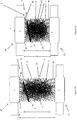
- FIGS 1A and 1B schematically illustrate an electrical support 1 for at least one electrical contact pad 2.
- the support 1 comprises an insulating viscoelastic matrix 3.
- the support 1 also comprises at least one elastically deformable structure 4 made of a conductive material.
- each structure 4 forms an open web.
- an open web refers to interconnected elements leaving spaces between them, such as a foam, a network (such as a network of beams or strings), a scaffolding (such as a scaffolding of beams or strings) or a lattice (such as a lattice of beams or strings).
- Each structure 4 is conductive and the open web provides multiple points 44 of electrical contacts to the contact pad 2, as well as multiple conduction paths to and from the contact pad 2.
- each structure 4 is at least partly embedded in the matrix 3.
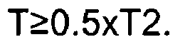
- the support 1 has a thickness T1 and in Figure 1B the support 1 has a thickness T2, however a thickness T of the matrix 3 may provide substantially a thickness of the support 1, i.e. the majority of the thicknesses T1 or T2 of the support 1 is formed from the thickness T of the matrix 3, and T is substantially constant even when the support 1 is subjected to a load L (as illustrated in Figure 1B ).
- T ⁇ 0.5 ⁇ T 1 and/or T ⁇ 0.5 ⁇ T 2.
- the matrix 3 also provides mechanical reinforcement to the at least one structure 4 and chemical stability to the at least one structure 4.
- the matrix 3 enables maintaining the structural stability of the open web structure 4.
- the matrix 3 enables maintaining the spaces between the interconnected elements of the open web structure 4.
- Each structure 4 comprises at least:
- Each structure 4 comprises a stiffer section 43 corresponding substantially to the core part 5 of the structure 4.
- the stiffer section 43 reinforces the structure 4 against over compression under the load L applied to the support 1, as illustrated in Figure 1B . It should be understood that, in some examples, the stiffer section 43 may extend outside the matrix 3.
- each structure 4 also comprises at least one more flexible section 42 corresponding substantially to the at least one connection part 6 of the structure 4.
- Each structure 4 is elastically deformable, and the more flexible section 42, substantially not embedded in the matrix 3, provides compliance with deformations the support 1 undergoes when subjected to the load L, as illustrated in Figure 1B with T2 ⁇ T1.
- the matrix 3 enables maintaining and enhancing the elastic compliancy of the open web structure 4. It should be understood that, in some examples, the more flexible section 42 may be embedded in the matrix 3.
- the at least one more flexible section 42 substantially provides the multiple points 44 of electrical contacts to the contact pad 2, as well as multiple conduction paths to and from the contact pad 2 (in combination with the stiffer section 43).
- the viscoelastic matrix 3 is made of a material comprising a hydrophobic elastomer.
- the matrix 3 may provide a stop layer and may seal the support 1 from moisture and other contaminants.
- the structure 4 comprises a structure made of a carbon-based material.
- the material of the carbon-based structure may comprise a carbon allotrope.
- the carbon allotrope may comprise at least one of:
- the CNT may be single-walled or may comprise a plurality of walls and diameters.
- Non-limiting examples include at least one of double-walled carbon nanotubes (DWNTs) and/or multi-walled carbon nanotubes (MWCNTs).
- DWNTs double-walled carbon nanotubes
- MWCNTs multi-walled carbon nanotubes
- the CNTs may be hybridized with other carbon allotropes, and non-limiting examples of other carbon allotropes include fullerenes, graphitic foliates, graphene, the carbon allotropes thus forming other morphologies such as carbon nanobuds, carbon peapods, graphenated CNTs, graphene and CNTs 3D nanoarchitectures.
- Non-limiting examples of 3D nanoarchitectures include scaffoldings, foams and networks, such as pillared graphene.
- CNTs may be connected by themselves and/or integrated with other carbon allotropes by junctions or cross-linking. All of the above combinations may be incorporated in glassy carbon.
- the carbon-based structure may comprise a highly-ordered network of CNT.
- the carbon-based structure 4 may comprise a random network 7 of CNT.
- the random network of CNT may include CNT sponges.
- the carbon-based structure may comprise a glassy carbon nanolattice 8 and/or a CNT nanolattice 8.
- the glassy carbon nanolattice 8 further comprises a thin layer of metal to enhance the electrical conductivity of the nanolattice.
- the thin layer of metal may comprise a thin layer of at least one of lead, platinum, gold or titanium, but other metals are envisaged.
- one or more types of CNTs may be chosen among different types of CNTs in order to obtain suitable mechanical and electrical properties of the one or more structures 4.
- the different types of CNTs include at least one of CNTs with different numbers of walls, different chiralities, different beam or string diameters and/or different surface chemistries. It should be understood that chirality may have an impact directly on electrical properties of the CNTs, but may also have an impact indirectly on a size and a stability of the CNTs. It should be understood that surface properties may have an impact on how the CNTs conduct electricity and on how the CNTs react between themselves, with other carbon allotropes and/or with the matrix. The surface properties may also contribute to the architecture topology and stability of the structure, and may contribute to integration of the structure within the surrounding matrix.
- the structure may comprise a structure made of nanowires and/or nanofibers, as non-limiting examples.
- the nanowires and/or nanofibers may be composed of at least one of:
- the structure may comprise a structure made of nanowires and/or nanofibers composed of insulators (non-limiting examples include SiO2 and TiO2).
- Non-conductive nanowires and/or nanofibers may be used to improve the mechanical properties of the structures.
- the stiffer section 43 may comprise thicker beams or strings 45 than beams or strings in the more flexible section 42 (e.g. Figures 2A and 2B and Figures 3A and 3B ). Alternatively or additionally, the stiffer section 43 may comprise more beams or strings 46 which are substantially perpendicular to the at least one electrical contact pad 2 than the more flexible section 42 (e.g. Figures 3A and 3B ). In some examples, the stiffer section 43 may comprise a higher density 47 of the web than the more flexible section 42 (e.g. Figures 2A and 2B ). Alternatively or additionally, the stiffer section 43 may comprise more interconnections of the web than the more flexible section 42 (e.g. Figures 2A and 2B ). Differences may include differences in the topology and interconnections between the carbon allotropes obtained through different cross-linkers and junctions, in order to form 3D architectures with different densities and suitable mechanical properties.
- the stiffer section 43 may comprise one or more different types of CNTs compared to CNTs in the more flexible section 42. Differences may include at least one of different number of walls, chirality, diameter and/or surface chemistry as explained above.
- the stiffer section 43 may comprise a different combination of carbon allotropes (CNTs, graphene and hybrids as already stated) compared to the more flexible section 42. Differences may also include differences in the topology and interconnections between the carbon allotropes obtained through different cross-linkers and junctions in order to form 3D architectures with different densities and suitable mechanical properties. Differences may also comprise differences in the surface properties of the carbon allotropes compared to the surface properties of the ones in the more flexible section 42. The surface properties may contribute to the architecture topology and stability of the structure as well as the proper integration of the structure with the surrounding matrix and the electrical conductivity of the structure. Alternatively or additionally, the stiffer section may comprise a higher density of CNT than the more flexible section. Alternatively or additionally, the stiffer section may comprise a higher density of a nanolattice than the more flexible section.
- the support 1 may be configured to support two arrays 20 of e.g. only one pad 2. As illustrated in Figures 1A and 1B , the support 1 may be configured to support only one array 20.
- the support 1 may be configured to be an interposer between two arrays 20 of at least one electrical contact pad 2.
- the arrays 20 illustrated in Figures 2A, 2B , 3A and 3B comprise only one pad 2, but it should be understood that each array 20 could comprise a plurality of pads 2.
- connection part 42 of the structure 4 may be connected to a first array 20 of the two arrays 20.
- the structure 4 further comprises a second connection part 48 which extends out of the insulating matrix 3 and is configured to be connected to a second array 20 of the two arrays 20.
- the plurality of electrical contact pads 2 may be separated by a pitch P.
- P may be such that: 0 ⁇ P ⁇ 0.3 mm (i.e. 300 ⁇ m).
- the pitch P may be such that:
- the pitch P may be larger than 0.3 mm (300 ⁇ m).
- the thickness T of the insulating viscoelastic matrix 3 may be such that: 0 ⁇ T ⁇ 0.3 mm (i.e. 300 ⁇ m).
- the methods of manufacturing of the support enable scalability of the support, such that, in some examples, the thickness T may be such that:
- the thickness T may be larger than 0.3 mm (300 ⁇ m).
- the disclosure also relates to electrical devices comprising the electrical support 1 of any aspects of the disclosure and at least one electrical contact pad connected to the connection part 42 (or 48 when present) of the structure 4 of the support 1.
- Figure 4 schematically illustrates a method 100 of manufacturing an electrical support for at least one electrical contact pad.
- the method 100 comprises:
- the manufacturing is performed such that the structure comprises at least a core part which is embedded within the insulating matrix, and at least one connection part which extends out of the insulating matrix and is configured to be connected to the electrical contact pad.
- the manufacturing is performed such that the structure comprises a stiffer section corresponding substantially to the core part of the structure and at least one more flexible section corresponding substantially to the at least one connection part of the structure.
- the method 100 may be performed to manufacture the support 1 of any aspects of the disclosure.
- the one or more structures may comprise one or more CNTs which may be single-walled or may comprise a plurality of walls and diameters.
- the CNTs may be hybridized with other carbon allotropes, and non-limiting examples of other carbon allotropes include fullerenes, graphitic foliates, graphene, the carbon allotropes thus forming other morphologies such as carbon nanobuds, carbon peapods, graphenated CNTs, a graphene and/or CNTs 3D nanoarchitectures.
- Non-limiting examples of 3D nanoarchitectures include scaffoldings, foams and networks, such as pillared graphene.
- CNTs may be connected by themselves and/or integrated with other carbon allotropes by junctions or cross-linking. All of the above combinations may be incorporated in glassy carbon.
- the one or more structure may also comprise a structure made of nanowires and/or nanofibers.
- manufacturing the one or more structures at S1 may comprise enabling the one or more structures to self-assemble in a highly-ordered network or a random network.
- manufacturing the one or more structures at S1 may comprise engineering one or more initial structures by 3D lithography and obtaining one or more final structures using pyrolysis.
- manufacturing the one or more structures at S1 and the matrix at S2 may comprise engineering one or more initial structures by 3D lithography by embedding the one or more structures inside an insulating viscoelastic matrix and obtaining one or more structures using pyrolysis.
- the method 100 enables scalability of the support to predetermined and desired dimensions. Alternatively or additionally, the method 100 enables engineering of the mechanical, chemical and/or conductive properties of the support to predetermined and desired properties.
- the manufacturing at S1 of the structure further comprises depositing a thin layer of metal on the glassy carbon nanolattice to enhance the electrical conductivity of the nanolattice.
- the thin layer of metal may comprise a thin layer of at least one of lead, platinum, gold or titanium, but other metals are envisaged.
- depositing the thin layer of metal may be performed by Atomic Layer Deposition, ALD, but other methods may be envisaged.
- the support of any aspects of the disclosure may be configured to be used in at least one of:
Landscapes
- Engineering & Computer Science (AREA)
- Manufacturing & Machinery (AREA)
- Carbon And Carbon Compounds (AREA)
- Laminated Bodies (AREA)
- Non-Insulated Conductors (AREA)
Abstract
Description
- The invention relates, but is not limited to, an electrical support for at least one electrical contact pad. The invention also relates to a method of manufacture of such a support.
- Known electrical supports enable electrical conduction to or from at least one electrical contact pad, such as a contact pad for a chip. Some supports may be used as interposers between printed circuit boards, PCB.
- Aspects and embodiments of the invention are set out in the appended claims. These and other aspects and embodiments of the invention are also described herein.
- Aspects of the disclosure will now be described, by way of example, with reference to the accompanying drawings in which:
-
Figure 1A is an elevation view, in a longitudinal cross section, which schematically illustrates an electrical support for at least one electrical contact pad according to the disclosure, not subjected to a load; -
Figure 1B is an elevation view, in a longitudinal cross section, which schematically illustrates the support ofFigure 1A subjected to a load; -
Figure 2A is an elevation view, in a longitudinal cross section, which schematically illustrates a first example electrical support according to the disclosure, not subjected to a load; -
Figure 2B is an elevation view, in a longitudinal cross section, which schematically illustrates the support ofFigure 2A subjected to a load; -
Figure 3A is an elevation view, in a longitudinal cross section, which schematically illustrates a second example electrical support according to the disclosure, not subjected to a load; -
Figure 3B is an elevation view, in a longitudinal cross section, which schematically illustrates the support ofFigure 3A subjected to a load; -
Figure 4 schematically illustrates example steps of a method of manufacture of a support of any one of the aspects of the disclosure. - In the drawings, similar elements bear identical numerical references.
- The disclosure relates but is not limited to an electrical support for at least one electrical contact pad. The support comprises an insulating viscoelastic matrix in which is partly embedded at least one elastically deformable structure made of a conductive material. Each of the structures forms an open web, such as a foam, a network, a scaffolding or a lattice. Each structure comprises a stiffer section corresponding substantially to a part of the structure which is embedded in the matrix and a more flexible section corresponding substantially to a part of the structure which is connected to the electrical contact pad, outside the matrix.
- The matrix provides substantially a thickness of the support, mechanical reinforcement to the structures and chemical stability to the structures.
- Each structure is conductive and the open web provides multiple points of electrical contacts to the contact pad, as well as multiple conduction paths to and from the contact pad.
- Each structure is elastically deformable and the more flexible section not embedded in the matrix provides compliance with deformations under which the support undergoes when subjected to a load. However the stiffer section reinforces the structure against over compression under the load and limits wear damage to the support.
- The matrix may comprise a hydrophobic material and may provide a stop layer and may seal the support from moisture and other contaminants.
-
Figures 1A and 1B schematically illustrate anelectrical support 1 for at least oneelectrical contact pad 2. - The
support 1 comprises an insulatingviscoelastic matrix 3. - The
support 1 also comprises at least one elasticallydeformable structure 4 made of a conductive material. - As illustrated in
Figures 1A and 1B , eachstructure 4 forms an open web. In the context of the present disclosure, an open web refers to interconnected elements leaving spaces between them, such as a foam, a network (such as a network of beams or strings), a scaffolding (such as a scaffolding of beams or strings) or a lattice (such as a lattice of beams or strings). - Each
structure 4 is conductive and the open web providesmultiple points 44 of electrical contacts to thecontact pad 2, as well as multiple conduction paths to and from thecontact pad 2. - Each
structure 4 is at least partly embedded in thematrix 3. InFigure 1A thesupport 1 has a thickness T1 and inFigure 1B thesupport 1 has a thickness T2, however a thickness T of thematrix 3 may provide substantially a thickness of thesupport 1, i.e. the majority of the thicknesses T1 or T2 of thesupport 1 is formed from the thickness T of thematrix 3, and T is substantially constant even when thesupport 1 is subjected to a load L (as illustrated inFigure 1B ). In some non-limiting examples,
- The
matrix 3 also provides mechanical reinforcement to the at least onestructure 4 and chemical stability to the at least onestructure 4. Thematrix 3 enables maintaining the structural stability of theopen web structure 4. Thematrix 3 enables maintaining the spaces between the interconnected elements of theopen web structure 4. - Each
structure 4 comprises at least: - a
core part 5 which is embedded within theinsulating matrix 3, and - at least one
connection part 6 which extends out of theinsulating matrix 3 and is configured to be connected to the at least oneelectrical contact pad 2. - Each
structure 4 comprises astiffer section 43 corresponding substantially to thecore part 5 of thestructure 4. Thestiffer section 43 reinforces thestructure 4 against over compression under the load L applied to thesupport 1, as illustrated inFigure 1B . It should be understood that, in some examples, thestiffer section 43 may extend outside thematrix 3. - Alternatively or additionally, each
structure 4 also comprises at least one moreflexible section 42 corresponding substantially to the at least oneconnection part 6 of thestructure 4. Eachstructure 4 is elastically deformable, and the moreflexible section 42, substantially not embedded in thematrix 3, provides compliance with deformations thesupport 1 undergoes when subjected to the load L, as illustrated inFigure 1B with T2<T1. Thematrix 3 enables maintaining and enhancing the elastic compliancy of theopen web structure 4. It should be understood that, in some examples, the moreflexible section 42 may be embedded in thematrix 3. - The at least one more
flexible section 42 substantially provides themultiple points 44 of electrical contacts to thecontact pad 2, as well as multiple conduction paths to and from the contact pad 2 (in combination with the stiffer section 43). - In some examples, the
viscoelastic matrix 3 is made of a material comprising a hydrophobic elastomer. Thematrix 3 may provide a stop layer and may seal thesupport 1 from moisture and other contaminants. - In some examples, the
structure 4 comprises a structure made of a carbon-based material. In such examples, the material of the carbon-based structure may comprise a carbon allotrope. The carbon allotrope may comprise at least one of: - one or more carbon nanotubes, CNT;
- one or more carbon nanobuds;
- one or more carbon peapods;
- one or more graphenated one or more CNTs;
- one or more 3D nanoarchitectures comprising a mix of graphene and CNTs;
- a glassy carbon;
- a graphene;
- one or more fullerenes;
- one or more graphitic foliates; and/or
- a carbon nanofoam.
- The CNT may be single-walled or may comprise a plurality of walls and diameters. Non-limiting examples include at least one of double-walled carbon nanotubes (DWNTs) and/or multi-walled carbon nanotubes (MWCNTs).
- As stated above, the CNTs may be hybridized with other carbon allotropes, and non-limiting examples of other carbon allotropes include fullerenes, graphitic foliates, graphene, the carbon allotropes thus forming other morphologies such as carbon nanobuds, carbon peapods, graphenated CNTs, graphene and CNTs 3D nanoarchitectures. Non-limiting examples of 3D nanoarchitectures include scaffoldings, foams and networks, such as pillared graphene. CNTs may be connected by themselves and/or integrated with other carbon allotropes by junctions or cross-linking. All of the above combinations may be incorporated in glassy carbon.
- In some examples, the carbon-based structure may comprise a highly-ordered network of CNT. Alternatively or additionally, as illustrated in
Figures 2A and 2B , the carbon-basedstructure 4 may comprise arandom network 7 of CNT. In some examples, the random network of CNT may include CNT sponges. - Alternatively or additionally, as illustrated in
Figures 3A and 3B , the carbon-based structure may comprise aglassy carbon nanolattice 8 and/or aCNT nanolattice 8. - In some examples, the
glassy carbon nanolattice 8 further comprises a thin layer of metal to enhance the electrical conductivity of the nanolattice. The thin layer of metal may comprise a thin layer of at least one of lead, platinum, gold or titanium, but other metals are envisaged. - Alternatively or additionally, one or more types of CNTs may be chosen among different types of CNTs in order to obtain suitable mechanical and electrical properties of the one or
more structures 4. The different types of CNTs include at least one of CNTs with different numbers of walls, different chiralities, different beam or string diameters and/or different surface chemistries. It should be understood that chirality may have an impact directly on electrical properties of the CNTs, but may also have an impact indirectly on a size and a stability of the CNTs. It should be understood that surface properties may have an impact on how the CNTs conduct electricity and on how the CNTs react between themselves, with other carbon allotropes and/or with the matrix. The surface properties may also contribute to the architecture topology and stability of the structure, and may contribute to integration of the structure within the surrounding matrix. - Alternatively or additionally, the structure may comprise a structure made of nanowires and/or nanofibers, as non-limiting examples. The nanowires and/or nanofibers may be composed of at least one of:
- one or more metals (non-limiting examples include silver, tungsten, nickel, copper, gold, zinc, platinum, tin and relative alloys);
- semiconductors (non-limiting examples include silicon, indium phosphide, gallium nitride or carbon); and/or
- superconductors (such as yttrium barium copper oxide YBCO).
- Alternatively or additionally, the structure may comprise a structure made of nanowires and/or nanofibers composed of insulators (non-limiting examples include SiO2 and TiO2). Non-conductive nanowires and/or nanofibers may be used to improve the mechanical properties of the structures.
- In some examples, the
stiffer section 43 may comprise thicker beams orstrings 45 than beams or strings in the more flexible section 42 (e.g.Figures 2A and 2B andFigures 3A and 3B ). Alternatively or additionally, thestiffer section 43 may comprise more beams orstrings 46 which are substantially perpendicular to the at least oneelectrical contact pad 2 than the more flexible section 42 (e.g.Figures 3A and 3B ). In some examples, thestiffer section 43 may comprise ahigher density 47 of the web than the more flexible section 42 (e.g.Figures 2A and 2B ). Alternatively or additionally, thestiffer section 43 may comprise more interconnections of the web than the more flexible section 42 (e.g.Figures 2A and 2B ). Differences may include differences in the topology and interconnections between the carbon allotropes obtained through different cross-linkers and junctions, in order to form 3D architectures with different densities and suitable mechanical properties. - Alternatively or additionally, the
stiffer section 43 may comprise one or more different types of CNTs compared to CNTs in the moreflexible section 42. Differences may include at least one of different number of walls, chirality, diameter and/or surface chemistry as explained above. - Alternatively or additionally, the
stiffer section 43 may comprise a different combination of carbon allotropes (CNTs, graphene and hybrids as already stated) compared to the moreflexible section 42. Differences may also include differences in the topology and interconnections between the carbon allotropes obtained through different cross-linkers and junctions in order to form 3D architectures with different densities and suitable mechanical properties. Differences may also comprise differences in the surface properties of the carbon allotropes compared to the surface properties of the ones in the moreflexible section 42. The surface properties may contribute to the architecture topology and stability of the structure as well as the proper integration of the structure with the surrounding matrix and the electrical conductivity of the structure.
Alternatively or additionally, the stiffer section may comprise a higher density of CNT than the more flexible section. Alternatively or additionally, the stiffer section may comprise a higher density of a nanolattice than the more flexible section. - As illustrated in
Figures 2A, 2B ,3A and 3B , thesupport 1 may be configured to support twoarrays 20 of e.g. only onepad 2. As illustrated inFigures 1A and 1B , thesupport 1 may be configured to support only onearray 20. - As illustrated in
Figures 2A, 2B ,3A and 3B , thesupport 1 may be configured to be an interposer between twoarrays 20 of at least oneelectrical contact pad 2. Thearrays 20 illustrated inFigures 2A, 2B ,3A and 3B comprise only onepad 2, but it should be understood that eacharray 20 could comprise a plurality ofpads 2. - As illustrated in
Figures 2A, 2B ,3A and 3B , theconnection part 42 of thestructure 4 may be connected to afirst array 20 of the twoarrays 20. Thestructure 4 further comprises asecond connection part 48 which extends out of the insulatingmatrix 3 and is configured to be connected to asecond array 20 of the twoarrays 20. - As illustrated in
Figures 1A and 1B , the plurality ofelectrical contact pads 2 may be separated by a pitch P. In some examples, P may be such that:
0 < P ≤ 0.3 mm (i.e. 300 µm). - As explained in greater detail below, methods of manufacturing of the support, according to the disclosure, enable scalability of the support, such that, in some examples, the pitch P may be such that:
- 0 < P ≤ 0.01 mm (10 µm), or
- 0 < P < 0.001 mm (i.e. submicron pitch).
- Other dimensions may be envisaged, and the pitch P may be larger than 0.3 mm (300 µm).
- Alternatively or additionally, the thickness T of the insulating
viscoelastic matrix 3 may be such that:
0 < T ≤ 0.3 mm (i.e. 300 µm). - As already stated, the methods of manufacturing of the support, according to the disclosure, enable scalability of the support, such that, in some examples, the thickness T may be such that:
- 0 < T ≤ 0.01 mm (10 µm), or
- 0 < T < 0.001 mm (i.e. submicron thickness).
- Other dimensions may be envisaged, and the thickness T may be larger than 0.3 mm (300 µm).
- The disclosure also relates to electrical devices comprising the
electrical support 1 of any aspects of the disclosure and at least one electrical contact pad connected to the connection part 42 (or 48 when present) of thestructure 4 of thesupport 1. -
Figure 4 schematically illustrates amethod 100 of manufacturing an electrical support for at least one electrical contact pad. - The
method 100 comprises: - manufacturing, at S1, at least one elastically deformable, open web structure made of a conductive material; and
- manufacturing, at S2, an insulating viscoelastic matrix.
- At S2, the manufacturing is performed such that the structure comprises at least a core part which is embedded within the insulating matrix, and at least one connection part which extends out of the insulating matrix and is configured to be connected to the electrical contact pad. At S2, the manufacturing is performed such that the structure comprises a stiffer section corresponding substantially to the core part of the structure and at least one more flexible section corresponding substantially to the at least one connection part of the structure.
- The
method 100 may be performed to manufacture thesupport 1 of any aspects of the disclosure. - As already stated, the one or more structures may comprise one or more CNTs which may be single-walled or may comprise a plurality of walls and diameters. The CNTs may be hybridized with other carbon allotropes, and non-limiting examples of other carbon allotropes include fullerenes, graphitic foliates, graphene, the carbon allotropes thus forming other morphologies such as carbon nanobuds, carbon peapods, graphenated CNTs, a graphene and/or CNTs 3D nanoarchitectures. Non-limiting examples of 3D nanoarchitectures include scaffoldings, foams and networks, such as pillared graphene. CNTs may be connected by themselves and/or integrated with other carbon allotropes by junctions or cross-linking. All of the above combinations may be incorporated in glassy carbon. The one or more structure may also comprise a structure made of nanowires and/or nanofibers.
- In some non-limiting examples, manufacturing the one or more structures at S1 may comprise enabling the one or more structures to self-assemble in a highly-ordered network or a random network. Alternatively or additionally, manufacturing the one or more structures at S1 may comprise engineering one or more initial structures by 3D lithography and obtaining one or more final structures using pyrolysis. Alternatively or additionally, manufacturing the one or more structures at S1 and the matrix at S2 may comprise engineering one or more initial structures by 3D lithography by embedding the one or more structures inside an insulating viscoelastic matrix and obtaining one or more structures using pyrolysis.
- The
method 100 enables scalability of the support to predetermined and desired dimensions. Alternatively or additionally, themethod 100 enables engineering of the mechanical, chemical and/or conductive properties of the support to predetermined and desired properties. - In some examples, the manufacturing at S1 of the structure further comprises depositing a thin layer of metal on the glassy carbon nanolattice to enhance the electrical conductivity of the nanolattice. The thin layer of metal may comprise a thin layer of at least one of lead, platinum, gold or titanium, but other metals are envisaged. In some non-limiting examples, depositing the thin layer of metal may be performed by Atomic Layer Deposition, ALD, but other methods may be envisaged.
- The support of any aspects of the disclosure may be configured to be used in at least one of:
- a Land Grid Array, LGA,
- a board-to-board connector, such as an interposer,
- a board-to-flex connector, such as an interposer,
- an application-specific integrated circuit, ASIC,
- a device with a pin count of up to several thousand I/O, and/or
- an anisotropic conductive film for flip-chip integrated circuit, IC, assembly.
- The above examples are non-limiting and other applications may be envisaged.
Claims (15)
- An electrical support for at least one electrical contact pad, comprising:an insulating viscoelastic matrix; andat least one elastically deformable structure made of a conductive material to form an open web, the at least one structure comprising at least:a core part which is embedded within the insulating matrix, andat least one connection part which extends out of the insulating matrix and is configured to be connected to the at least one electrical contact pad,wherein the structure comprises a stiffer section corresponding substantially to the core part of the structure and at least one more flexible section corresponding substantially to the at least one connection part of the structure.
- The support of claim 1, wherein the viscoelastic matrix is made of a material comprising a hydrophobic elastomer.
- The support of any one of the preceding claims, wherein the structure comprises a structure made of a carbon-based material, optionally wherein the material of the carbon-based structure comprises at least one carbon allotrope.
- The support of claim 3, wherein the at least one carbon allotrope comprises at least one of:one or more carbon nanotubes, CNTs;one or more carbon nanobuds;one or more carbon peapods;one or more graphenated one or more CNTs;one or more 3D nanoarchitectures comprising a mix of graphene and at least one CNT;a glassy carbon;a graphene;one or more fullerenes;one or more graphitic foliates; and/ora carbon nanofoam,optionally wherein the carbon-based structure comprises a highly-ordered or random network of CNTs, including CNT sponges, or optionally wherein the carbon-based structure comprises a glassy carbon nanolattice and/or a CNT nanolattice, optionally wherein the glassy carbon nanolattice further comprises a thin layer of metal to enhance the electrical conductivity of the nanolattice, optionally wherein the thin layer of metal comprises a thin layer of at least one of lead, platinum, gold or titanium.
- The support of any one of the preceding claims, wherein the structure comprises a structure made of nanowires and/or nanofibers, such as nanowires and/or nanofibers composed of at least one of:one or more metals;semiconductors; and/orsuperconductors.
- The support of any one of the preceding claims, wherein the stiffer section comprises at least one of:thicker beams or strings than beams or strings in the more flexible section; and/ormore beams or strings which are substantially perpendicular to the at least one electrical contact pad than the more flexible section;more interconnections of the web than the more flexible section; and/ora higher density of the web than the more flexible section.
- The support of any one of claims 4 to 6, wherein the stiffer section comprises at least one of:one or different types of CNTs compared to CNTs in the more flexible section, comprising at least one of:a different chirality of CNTs compared to a chirality of CNTs in the more flexible section; and/ora different number of walls for the CNTs compared to a number of walls for the CNTs in the more flexible section;a different diameter of CNTs compared to a diameter of CNTs in the more flexible section; and/ordifferent surface properties of CNTs compared to surface properties of CNTs in the more flexible section;a different combination of carbon allotropes compared to the more flexible section, including differences in the topology and interconnections between the carbon allotropes and/or differences in surface properties of carbon allotropes; and/ora higher density of CNT than the more flexible section; and/ora higher density of a nanolattice than the more flexible section.
- The support of any one of the preceding claims, configured to be an interposer between two arrays of at least one electrical contact pad, a first connection part of the structure being configured to be connected to a first array of the two arrays of the at least one electrical contact pad, and
wherein the structure further comprises a second connection part which extends out of the insulating matrix and is configured to be connected to a second array of the two arrays of the at least one electrical contact pad. - The support of any one of the preceding claims, configured for at least one array comprising a plurality of electrical contact pads separated by a pitch P, wherein P is such that:
0 < P ≤ 0.3 mm,optionally wherein the pitch P is such that:
0 < P ≤ 0.01 mm,optionally wherein P is such that:
0 < P < 0.001 mm, orwherein the insulating viscoelastic matrix has a thickness T, wherein T is such that:
0 < T ≤ 0.3 mm,optionally wherein the thickness T is such that:
0 < T ≤ 0.01 mm,optionally wherein the thickness T is such that:
0 < T < 0.001 mm. - The support of any one of the preceding claims, configured to be used in at least one of:a Land Grid Array, LGA,a board-to-board connector, such as an interposer,a board-to-flex connector, such as an interposer,an application-specific integrated circuit, ASIC,a device with a pin count of up to several thousand I/O,an anisotropic conductive film for flip-chip integrated circuit, IC, assembly.
- An electrical device, comprising:the electrical support of any one of the preceding claims; andat least one electrical contact pad connected to the connection part of the structure of the support.
- A method of manufacturing an electrical support for at least one electrical contact pad, comprising:manufacturing at least one elastically deformable, open web structure made of a conductive material; andmanufacturing an insulating viscoelastic matrix, such that the at least one structure comprises at least:a core part which is embedded within the insulating matrix, andat least one connection part which extends out of the insulating matrix and is configured to be connected to the electrical contact pad,wherein the structure comprises a stiffer section corresponding substantially to the core part of the structure and at least one more flexible section corresponding substantially to the at least one connection part of the structure.
- The method of claim 12, for manufacturing the support of any one of claims 1 to 10.
- The method of claim 12 or 13, wherein manufacturing the at least one structure comprises using a least one of:enabling one or more structures to self-assemble in a highly-ordered or random network; and/orengineering one or more initial structures by 3D lithography and obtaining one or more final structures using pyrolysis; and/orengineering one or more initial structures by 3D lithography by embedding the one or more initial structures inside an insulating viscoelastic matrix and obtaining one or more final structures using pyrolysis.
- The method of claim 14, wherein the manufacturing of the at least one structure further comprises depositing a thin layer of metal to enhance the electrical conductivity, optionally further comprising depositing the thin layer of metal by Atomic Layer Deposition, ALD.
Priority Applications (5)
| Application Number | Priority Date | Filing Date | Title |
|---|---|---|---|
| EP19425049.4A EP3761347B1 (en) | 2019-07-04 | 2019-07-04 | Open web electrical support for contact pad and method of manufacture |
| PCT/EP2020/068830 WO2021001537A1 (en) | 2019-07-04 | 2020-07-03 | Open web electrical support for contact pad and method of manufacture |
| CN202080061424.2A CN114830304A (en) | 2019-07-04 | 2020-07-03 | Open mesh electrical support for contact pads and method of manufacture |
| US17/623,769 US20220246510A1 (en) | 2019-07-04 | 2020-07-03 | Open web electrical support for contact pad and method of manufacture |
| US18/951,822 US20250140670A1 (en) | 2019-07-04 | 2024-11-19 | Open web electrical support for contact pad and method of manufacture |
Applications Claiming Priority (1)
| Application Number | Priority Date | Filing Date | Title |
|---|---|---|---|
| EP19425049.4A EP3761347B1 (en) | 2019-07-04 | 2019-07-04 | Open web electrical support for contact pad and method of manufacture |
Publications (3)
| Publication Number | Publication Date |
|---|---|
| EP3761347A1 true EP3761347A1 (en) | 2021-01-06 |
| EP3761347B1 EP3761347B1 (en) | 2025-11-19 |
| EP3761347C0 EP3761347C0 (en) | 2025-11-19 |
Family
ID=67847666
Family Applications (1)
| Application Number | Title | Priority Date | Filing Date |
|---|---|---|---|
| EP19425049.4A Active EP3761347B1 (en) | 2019-07-04 | 2019-07-04 | Open web electrical support for contact pad and method of manufacture |
Country Status (4)
| Country | Link |
|---|---|
| US (2) | US20220246510A1 (en) |
| EP (1) | EP3761347B1 (en) |
| CN (1) | CN114830304A (en) |
| WO (1) | WO2021001537A1 (en) |
Citations (8)
| Publication number | Priority date | Publication date | Assignee | Title |
|---|---|---|---|---|
| US20050142933A1 (en) * | 2003-12-17 | 2005-06-30 | Gottfried Beer | Flexible rewiring plate for semiconductor components, and process for producing it |
| US20050208785A1 (en) * | 2004-03-18 | 2005-09-22 | International Business Machines Corporation | Land grid array (LGA) interposer with adhesive-retained contacts and method of manufacture |
| US20050282409A1 (en) * | 2004-06-22 | 2005-12-22 | International Business Machines Corporation | Non-oriented wire in elastomer electrical contact |
| US20060234056A1 (en) * | 2005-04-14 | 2006-10-19 | Tsinghua University | Thermal interface material and method for making the same |
| EP2061077A2 (en) * | 2007-10-22 | 2009-05-20 | Fujitsu Limited | Sheet structure and method of manufacturing the same |
| US20110039459A1 (en) * | 2009-08-11 | 2011-02-17 | Yancey Jerry W | Solderless carbon nanotube and nanowire electrical contacts and methods of use thereof |
| WO2011123717A1 (en) * | 2010-03-31 | 2011-10-06 | Georgia Tech Research Corporation | Interconnect structures and methods of making the same |
| US20140302579A1 (en) * | 2011-10-07 | 2014-10-09 | Commissariat A L'Energie Atomique Et Aux | Device comprising a composite material and having nanotubes that are subjected to an electric field, and uses thereof |
Family Cites Families (10)
| Publication number | Priority date | Publication date | Assignee | Title |
|---|---|---|---|---|
| US4643499A (en) * | 1985-09-04 | 1987-02-17 | At&T Bell Laboratories | Component mounting apparatus |
| US4988306A (en) * | 1989-05-16 | 1991-01-29 | Labinal Components And Systems, Inc. | Low-loss electrical interconnects |
| US5599193A (en) * | 1994-08-23 | 1997-02-04 | Augat Inc. | Resilient electrical interconnect |
| US5701233A (en) * | 1995-01-23 | 1997-12-23 | Irvine Sensors Corporation | Stackable modules and multimodular assemblies |
| EP1061608A3 (en) * | 1999-05-10 | 2002-10-02 | Hirose Electric Co., Ltd. | Board to board electrical connectors |
| US6264476B1 (en) * | 1999-12-09 | 2001-07-24 | High Connection Density, Inc. | Wire segment based interposer for high frequency electrical connection |
| US6799977B2 (en) * | 2002-07-11 | 2004-10-05 | Hewlett-Packard Development Company, L.P. | Socket having foam metal contacts |
| US7029288B2 (en) * | 2003-03-24 | 2006-04-18 | Che-Yu Li | Electrical contact and connector and method of manufacture |
| US7510401B2 (en) * | 2006-10-12 | 2009-03-31 | Tessera, Inc. | Microelectronic component with foam-metal posts |
| IT201700100522A1 (en) * | 2017-09-07 | 2019-03-07 | Technoprobe Spa | Interface element for an electronic device test device and its manufacturing method |
-
2019
- 2019-07-04 EP EP19425049.4A patent/EP3761347B1/en active Active
-
2020
- 2020-07-03 CN CN202080061424.2A patent/CN114830304A/en active Pending
- 2020-07-03 US US17/623,769 patent/US20220246510A1/en not_active Abandoned
- 2020-07-03 WO PCT/EP2020/068830 patent/WO2021001537A1/en not_active Ceased
-
2024
- 2024-11-19 US US18/951,822 patent/US20250140670A1/en active Pending
Patent Citations (8)
| Publication number | Priority date | Publication date | Assignee | Title |
|---|---|---|---|---|
| US20050142933A1 (en) * | 2003-12-17 | 2005-06-30 | Gottfried Beer | Flexible rewiring plate for semiconductor components, and process for producing it |
| US20050208785A1 (en) * | 2004-03-18 | 2005-09-22 | International Business Machines Corporation | Land grid array (LGA) interposer with adhesive-retained contacts and method of manufacture |
| US20050282409A1 (en) * | 2004-06-22 | 2005-12-22 | International Business Machines Corporation | Non-oriented wire in elastomer electrical contact |
| US20060234056A1 (en) * | 2005-04-14 | 2006-10-19 | Tsinghua University | Thermal interface material and method for making the same |
| EP2061077A2 (en) * | 2007-10-22 | 2009-05-20 | Fujitsu Limited | Sheet structure and method of manufacturing the same |
| US20110039459A1 (en) * | 2009-08-11 | 2011-02-17 | Yancey Jerry W | Solderless carbon nanotube and nanowire electrical contacts and methods of use thereof |
| WO2011123717A1 (en) * | 2010-03-31 | 2011-10-06 | Georgia Tech Research Corporation | Interconnect structures and methods of making the same |
| US20140302579A1 (en) * | 2011-10-07 | 2014-10-09 | Commissariat A L'Energie Atomique Et Aux | Device comprising a composite material and having nanotubes that are subjected to an electric field, and uses thereof |
Also Published As
| Publication number | Publication date |
|---|---|
| US20250140670A1 (en) | 2025-05-01 |
| US20220246510A1 (en) | 2022-08-04 |
| CN114830304A (en) | 2022-07-29 |
| EP3761347B1 (en) | 2025-11-19 |
| EP3761347C0 (en) | 2025-11-19 |
| WO2021001537A1 (en) | 2021-01-07 |
Similar Documents
| Publication | Publication Date | Title |
|---|---|---|
| Li et al. | Carbon nanomaterials for next-generation interconnects and passives: Physics, status, and prospects | |
| US6856016B2 (en) | Method and apparatus using nanotubes for cooling and grounding die | |
| Jamond et al. | Piezo-generator integrating a vertical array of GaN nanowires | |
| Wang et al. | Fabrication and electrical and mechanical properties of carbon nanotube interconnections | |
| Xu et al. | Modeling, analysis, and design of graphene nano-ribbon interconnects | |
| Hu et al. | Tunable Schottky contacts in hybrid graphene–phosphorene nanocomposites | |
| EP2162910B1 (en) | A thermal interface material | |
| KR101004189B1 (en) | Methods of Forming Carbon Nanotube Architectures and Composites with High Electrical Conductivity and Thermal Conductivity and Structures Formed thereby | |
| US7960653B2 (en) | Conductive nanowires for electrical interconnect | |
| US10211758B2 (en) | Friction electric generator and manufacturing method thereof | |
| DE10359424B4 (en) | Redistribution board for narrow pitch semiconductor devices and method of making the same | |
| TWI730498B (en) | Connector for electrical connection | |
| Soga et al. | Carbon nanotube bumps for LSI interconnect | |
| KR101208032B1 (en) | Nano piezoelectric device and method of forming the same | |
| KR101858152B1 (en) | Heat radiation sheet and fabrication method thereof | |
| KR101110804B1 (en) | Method of forming a wiring structure | |
| Wilms et al. | Manipulation and conductivity measurements of gold nanowires | |
| US20250140670A1 (en) | Open web electrical support for contact pad and method of manufacture | |
| US11800602B1 (en) | Multilayered metal nanowire array | |
| KR20070089912A (en) | Electrical circuits having nanostructures and methods of contacting nanostructures | |
| JP6806328B2 (en) | Electronic device | |
| US11751367B2 (en) | Microelectronic package electrostatic discharge (ESD) protection | |
| Jiang et al. | Energy harvesting and temperature sensing thermoelectric devices based on the carbon template method | |
| Yuan et al. | 49‐3L: Late‐News Paper: Flexible and stretchable hybrid electronics systems for wearable applications | |
| Santini et al. | Growth and electrical characterization of horizontally aligned CNTs |
Legal Events
| Date | Code | Title | Description |
|---|---|---|---|
| PUAI | Public reference made under article 153(3) epc to a published international application that has entered the european phase |
Free format text: ORIGINAL CODE: 0009012 |
|
| STAA | Information on the status of an ep patent application or granted ep patent |
Free format text: STATUS: THE APPLICATION HAS BEEN PUBLISHED |
|
| AK | Designated contracting states |
Kind code of ref document: A1 Designated state(s): AL AT BE BG CH CY CZ DE DK EE ES FI FR GB GR HR HU IE IS IT LI LT LU LV MC MK MT NL NO PL PT RO RS SE SI SK SM TR |
|
| AX | Request for extension of the european patent |
Extension state: BA ME |
|
| STAA | Information on the status of an ep patent application or granted ep patent |
Free format text: STATUS: REQUEST FOR EXAMINATION WAS MADE |
|
| 17P | Request for examination filed |
Effective date: 20210705 |
|
| RBV | Designated contracting states (corrected) |
Designated state(s): AL AT BE BG CH CY CZ DE DK EE ES FI FR GB GR HR HU IE IS IT LI LT LU LV MC MK MT NL NO PL PT RO RS SE SI SK SM TR |
|
| GRAP | Despatch of communication of intention to grant a patent |
Free format text: ORIGINAL CODE: EPIDOSNIGR1 |
|
| STAA | Information on the status of an ep patent application or granted ep patent |
Free format text: STATUS: GRANT OF PATENT IS INTENDED |
|
| INTG | Intention to grant announced |
Effective date: 20250604 |
|
| GRAS | Grant fee paid |
Free format text: ORIGINAL CODE: EPIDOSNIGR3 |
|
| GRAA | (expected) grant |
Free format text: ORIGINAL CODE: 0009210 |
|
| STAA | Information on the status of an ep patent application or granted ep patent |
Free format text: STATUS: THE PATENT HAS BEEN GRANTED |
|
| AK | Designated contracting states |
Kind code of ref document: B1 Designated state(s): AL AT BE BG CH CY CZ DE DK EE ES FI FR GB GR HR HU IE IS IT LI LT LU LV MC MK MT NL NO PL PT RO RS SE SI SK SM TR |
|
| REG | Reference to a national code |
Ref country code: CH Ref legal event code: F10 Free format text: ST27 STATUS EVENT CODE: U-0-0-F10-F00 (AS PROVIDED BY THE NATIONAL OFFICE) Effective date: 20251119 Ref country code: GB Ref legal event code: FG4D |
|
| REG | Reference to a national code |
Ref country code: IE Ref legal event code: FG4D |
|
| U01 | Request for unitary effect filed |
Effective date: 20251125 |
|
| U07 | Unitary effect registered |
Designated state(s): AT BE BG DE DK EE FI FR IT LT LU LV MT NL PT RO SE SI Effective date: 20251201 |
|
| PG25 | Lapsed in a contracting state [announced via postgrant information from national office to epo] |
Ref country code: ES Free format text: LAPSE BECAUSE OF FAILURE TO SUBMIT A TRANSLATION OF THE DESCRIPTION OR TO PAY THE FEE WITHIN THE PRESCRIBED TIME-LIMIT Effective date: 20251119 |
|
| PG25 | Lapsed in a contracting state [announced via postgrant information from national office to epo] |
Ref country code: NO Free format text: LAPSE BECAUSE OF FAILURE TO SUBMIT A TRANSLATION OF THE DESCRIPTION OR TO PAY THE FEE WITHIN THE PRESCRIBED TIME-LIMIT Effective date: 20260219 |
|
| PG25 | Lapsed in a contracting state [announced via postgrant information from national office to epo] |
Ref country code: HR Free format text: LAPSE BECAUSE OF FAILURE TO SUBMIT A TRANSLATION OF THE DESCRIPTION OR TO PAY THE FEE WITHIN THE PRESCRIBED TIME-LIMIT Effective date: 20251119 |
|
| PG25 | Lapsed in a contracting state [announced via postgrant information from national office to epo] |
Ref country code: RS Free format text: LAPSE BECAUSE OF FAILURE TO SUBMIT A TRANSLATION OF THE DESCRIPTION OR TO PAY THE FEE WITHIN THE PRESCRIBED TIME-LIMIT Effective date: 20260219 |
|
| PG25 | Lapsed in a contracting state [announced via postgrant information from national office to epo] |
Ref country code: IS Free format text: LAPSE BECAUSE OF FAILURE TO SUBMIT A TRANSLATION OF THE DESCRIPTION OR TO PAY THE FEE WITHIN THE PRESCRIBED TIME-LIMIT Effective date: 20260319 |
|
| PG25 | Lapsed in a contracting state [announced via postgrant information from national office to epo] |
Ref country code: PL Free format text: LAPSE BECAUSE OF FAILURE TO SUBMIT A TRANSLATION OF THE DESCRIPTION OR TO PAY THE FEE WITHIN THE PRESCRIBED TIME-LIMIT Effective date: 20251119 |