EP2061077A2 - Sheet structure and method of manufacturing the same - Google Patents
Sheet structure and method of manufacturing the same Download PDFInfo
- Publication number
- EP2061077A2 EP2061077A2 EP08167274A EP08167274A EP2061077A2 EP 2061077 A2 EP2061077 A2 EP 2061077A2 EP 08167274 A EP08167274 A EP 08167274A EP 08167274 A EP08167274 A EP 08167274A EP 2061077 A2 EP2061077 A2 EP 2061077A2
- Authority
- EP
- European Patent Office
- Prior art keywords
- carbon nanotube
- bundles
- linear structure
- sheet
- substrate
- Prior art date
- Legal status (The legal status is an assumption and is not a legal conclusion. Google has not performed a legal analysis and makes no representation as to the accuracy of the status listed.)
- Granted
Links
- 238000004519 manufacturing process Methods 0.000 title claims description 58
- 125000004432 carbon atom Chemical group C* 0.000 claims abstract description 18
- 239000000758 substrate Substances 0.000 claims description 131
- 239000000463 material Substances 0.000 claims description 82
- 239000011248 coating agent Substances 0.000 claims description 55
- 238000000576 coating method Methods 0.000 claims description 55
- 229910052751 metal Inorganic materials 0.000 claims description 36
- 239000002184 metal Substances 0.000 claims description 36
- 230000003197 catalytic effect Effects 0.000 claims description 27
- 239000007788 liquid Substances 0.000 claims description 17
- 239000003054 catalyst Substances 0.000 claims description 7
- 238000004528 spin coating Methods 0.000 claims description 7
- 239000000945 filler Substances 0.000 claims description 2
- 238000001035 drying Methods 0.000 claims 2
- OKTJSMMVPCPJKN-UHFFFAOYSA-N Carbon Chemical compound [C] OKTJSMMVPCPJKN-UHFFFAOYSA-N 0.000 description 518
- 239000002041 carbon nanotube Substances 0.000 description 514
- 229910021393 carbon nanotube Inorganic materials 0.000 description 514
- 239000010408 film Substances 0.000 description 129
- 239000010410 layer Substances 0.000 description 108
- 239000004065 semiconductor Substances 0.000 description 27
- 239000010931 gold Substances 0.000 description 23
- 229920005989 resin Polymers 0.000 description 20
- 239000011347 resin Substances 0.000 description 20
- 238000000034 method Methods 0.000 description 16
- 239000010936 titanium Substances 0.000 description 16
- XEEYBQQBJWHFJM-UHFFFAOYSA-N iron Substances [Fe] XEEYBQQBJWHFJM-UHFFFAOYSA-N 0.000 description 14
- 229920002120 photoresistant polymer Polymers 0.000 description 14
- -1 acryl Chemical group 0.000 description 12
- PCHJSUWPFVWCPO-UHFFFAOYSA-N gold Chemical compound [Au] PCHJSUWPFVWCPO-UHFFFAOYSA-N 0.000 description 11
- 229910052737 gold Inorganic materials 0.000 description 11
- VYPSYNLAJGMNEJ-UHFFFAOYSA-N Silicium dioxide Chemical compound O=[Si]=O VYPSYNLAJGMNEJ-UHFFFAOYSA-N 0.000 description 10
- 239000003822 epoxy resin Substances 0.000 description 10
- 229920000647 polyepoxide Polymers 0.000 description 10
- ZWEHNKRNPOVVGH-UHFFFAOYSA-N 2-Butanone Chemical compound CCC(C)=O ZWEHNKRNPOVVGH-UHFFFAOYSA-N 0.000 description 9
- PXHVJJICTQNCMI-UHFFFAOYSA-N Nickel Chemical compound [Ni] PXHVJJICTQNCMI-UHFFFAOYSA-N 0.000 description 9
- 239000000470 constituent Substances 0.000 description 9
- 229910052738 indium Inorganic materials 0.000 description 9
- APFVFJFRJDLVQX-UHFFFAOYSA-N indium atom Chemical compound [In] APFVFJFRJDLVQX-UHFFFAOYSA-N 0.000 description 9
- 238000004380 ashing Methods 0.000 description 8
- 229910052814 silicon oxide Inorganic materials 0.000 description 8
- LFQSCWFLJHTTHZ-UHFFFAOYSA-N Ethanol Chemical compound CCO LFQSCWFLJHTTHZ-UHFFFAOYSA-N 0.000 description 7
- RTAQQCXQSZGOHL-UHFFFAOYSA-N Titanium Chemical compound [Ti] RTAQQCXQSZGOHL-UHFFFAOYSA-N 0.000 description 7
- 239000004020 conductor Substances 0.000 description 7
- 239000010949 copper Substances 0.000 description 7
- 230000005855 radiation Effects 0.000 description 7
- 238000004544 sputter deposition Methods 0.000 description 7
- 239000000126 substance Substances 0.000 description 7
- 229910052719 titanium Inorganic materials 0.000 description 7
- OKKJLVBELUTLKV-UHFFFAOYSA-N Methanol Chemical compound OC OKKJLVBELUTLKV-UHFFFAOYSA-N 0.000 description 6
- 230000003247 decreasing effect Effects 0.000 description 6
- BASFCYQUMIYNBI-UHFFFAOYSA-N platinum Substances [Pt] BASFCYQUMIYNBI-UHFFFAOYSA-N 0.000 description 6
- 229910052581 Si3N4 Inorganic materials 0.000 description 5
- QVGXLLKOCUKJST-UHFFFAOYSA-N atomic oxygen Chemical compound [O] QVGXLLKOCUKJST-UHFFFAOYSA-N 0.000 description 5
- 239000001301 oxygen Substances 0.000 description 5
- 229910052760 oxygen Inorganic materials 0.000 description 5
- HQVNEWCFYHHQES-UHFFFAOYSA-N silicon nitride Chemical compound N12[Si]34N5[Si]62N3[Si]51N64 HQVNEWCFYHHQES-UHFFFAOYSA-N 0.000 description 5
- RYGMFSIKBFXOCR-UHFFFAOYSA-N Copper Chemical compound [Cu] RYGMFSIKBFXOCR-UHFFFAOYSA-N 0.000 description 4
- XUIMIQQOPSSXEZ-UHFFFAOYSA-N Silicon Chemical compound [Si] XUIMIQQOPSSXEZ-UHFFFAOYSA-N 0.000 description 4
- NRTOMJZYCJJWKI-UHFFFAOYSA-N Titanium nitride Chemical compound [Ti]#N NRTOMJZYCJJWKI-UHFFFAOYSA-N 0.000 description 4
- 229910045601 alloy Inorganic materials 0.000 description 4
- 239000000956 alloy Substances 0.000 description 4
- 230000008859 change Effects 0.000 description 4
- 229910052802 copper Inorganic materials 0.000 description 4
- 230000000694 effects Effects 0.000 description 4
- 238000004050 hot filament vapor deposition Methods 0.000 description 4
- 239000007769 metal material Substances 0.000 description 4
- 238000000206 photolithography Methods 0.000 description 4
- 230000008569 process Effects 0.000 description 4
- 239000010703 silicon Substances 0.000 description 4
- 229910052710 silicon Inorganic materials 0.000 description 4
- 229920002050 silicone resin Polymers 0.000 description 4
- CSCPPACGZOOCGX-UHFFFAOYSA-N Acetone Chemical compound CC(C)=O CSCPPACGZOOCGX-UHFFFAOYSA-N 0.000 description 3
- KFZMGEQAYNKOFK-UHFFFAOYSA-N Isopropanol Chemical compound CC(C)O KFZMGEQAYNKOFK-UHFFFAOYSA-N 0.000 description 3
- BQCADISMDOOEFD-UHFFFAOYSA-N Silver Chemical compound [Ag] BQCADISMDOOEFD-UHFFFAOYSA-N 0.000 description 3
- PNEYBMLMFCGWSK-UHFFFAOYSA-N aluminium oxide Inorganic materials [O-2].[O-2].[O-2].[Al+3].[Al+3] PNEYBMLMFCGWSK-UHFFFAOYSA-N 0.000 description 3
- 229910052799 carbon Inorganic materials 0.000 description 3
- 238000004891 communication Methods 0.000 description 3
- 230000007423 decrease Effects 0.000 description 3
- 239000007789 gas Substances 0.000 description 3
- 239000011521 glass Substances 0.000 description 3
- 229910052742 iron Inorganic materials 0.000 description 3
- 229910052759 nickel Inorganic materials 0.000 description 3
- KDLHZDBZIXYQEI-UHFFFAOYSA-N palladium Substances [Pd] KDLHZDBZIXYQEI-UHFFFAOYSA-N 0.000 description 3
- 239000012466 permeate Substances 0.000 description 3
- 230000000717 retained effect Effects 0.000 description 3
- 229910052709 silver Inorganic materials 0.000 description 3
- 239000004332 silver Substances 0.000 description 3
- 229920001187 thermosetting polymer Polymers 0.000 description 3
- XKRFYHLGVUSROY-UHFFFAOYSA-N Argon Chemical compound [Ar] XKRFYHLGVUSROY-UHFFFAOYSA-N 0.000 description 2
- KRHYYFGTRYWZRS-UHFFFAOYSA-N Fluorane Chemical compound F KRHYYFGTRYWZRS-UHFFFAOYSA-N 0.000 description 2
- NBIIXXVUZAFLBC-UHFFFAOYSA-N Phosphoric acid Chemical compound OP(O)(O)=O NBIIXXVUZAFLBC-UHFFFAOYSA-N 0.000 description 2
- 239000000654 additive Substances 0.000 description 2
- 230000000996 additive effect Effects 0.000 description 2
- HSFWRNGVRCDJHI-UHFFFAOYSA-N alpha-acetylene Natural products C#C HSFWRNGVRCDJHI-UHFFFAOYSA-N 0.000 description 2
- 239000002482 conductive additive Substances 0.000 description 2
- 229920001940 conductive polymer Polymers 0.000 description 2
- 125000002534 ethynyl group Chemical group [H]C#C* 0.000 description 2
- 238000010438 heat treatment Methods 0.000 description 2
- 150000002576 ketones Chemical class 0.000 description 2
- 239000002923 metal particle Substances 0.000 description 2
- VNWKTOKETHGBQD-UHFFFAOYSA-N methane Chemical compound C VNWKTOKETHGBQD-UHFFFAOYSA-N 0.000 description 2
- 239000000203 mixture Substances 0.000 description 2
- 239000002048 multi walled nanotube Substances 0.000 description 2
- 239000010955 niobium Substances 0.000 description 2
- 229910052697 platinum Inorganic materials 0.000 description 2
- 238000005498 polishing Methods 0.000 description 2
- 229920000767 polyaniline Polymers 0.000 description 2
- 229920001721 polyimide Polymers 0.000 description 2
- 239000009719 polyimide resin Substances 0.000 description 2
- 229920000123 polythiophene Polymers 0.000 description 2
- 239000002994 raw material Substances 0.000 description 2
- 229910052594 sapphire Inorganic materials 0.000 description 2
- 239000010980 sapphire Substances 0.000 description 2
- 239000002356 single layer Substances 0.000 description 2
- 239000002109 single walled nanotube Substances 0.000 description 2
- 229910000679 solder Inorganic materials 0.000 description 2
- MZLGASXMSKOWSE-UHFFFAOYSA-N tantalum nitride Chemical compound [Ta]#N MZLGASXMSKOWSE-UHFFFAOYSA-N 0.000 description 2
- 239000010409 thin film Substances 0.000 description 2
- 239000004925 Acrylic resin Substances 0.000 description 1
- 229920000178 Acrylic resin Polymers 0.000 description 1
- XMWRBQBLMFGWIX-UHFFFAOYSA-N C60 fullerene Chemical compound C12=C3C(C4=C56)=C7C8=C5C5=C9C%10=C6C6=C4C1=C1C4=C6C6=C%10C%10=C9C9=C%11C5=C8C5=C8C7=C3C3=C7C2=C1C1=C2C4=C6C4=C%10C6=C9C9=C%11C5=C5C8=C3C3=C7C1=C1C2=C4C6=C2C9=C5C3=C12 XMWRBQBLMFGWIX-UHFFFAOYSA-N 0.000 description 1
- 229920000049 Carbon (fiber) Polymers 0.000 description 1
- 239000004593 Epoxy Substances 0.000 description 1
- VGGSQFUCUMXWEO-UHFFFAOYSA-N Ethene Chemical compound C=C VGGSQFUCUMXWEO-UHFFFAOYSA-N 0.000 description 1
- 239000005977 Ethylene Substances 0.000 description 1
- NTIZESTWPVYFNL-UHFFFAOYSA-N Methyl isobutyl ketone Chemical compound CC(C)CC(C)=O NTIZESTWPVYFNL-UHFFFAOYSA-N 0.000 description 1
- UIHCLUNTQKBZGK-UHFFFAOYSA-N Methyl isobutyl ketone Natural products CCC(C)C(C)=O UIHCLUNTQKBZGK-UHFFFAOYSA-N 0.000 description 1
- ZOKXTWBITQBERF-UHFFFAOYSA-N Molybdenum Chemical compound [Mo] ZOKXTWBITQBERF-UHFFFAOYSA-N 0.000 description 1
- 229910003087 TiOx Inorganic materials 0.000 description 1
- 229910008486 TiSix Inorganic materials 0.000 description 1
- GWEVSGVZZGPLCZ-UHFFFAOYSA-N Titan oxide Chemical compound O=[Ti]=O GWEVSGVZZGPLCZ-UHFFFAOYSA-N 0.000 description 1
- 238000005411 Van der Waals force Methods 0.000 description 1
- QCWXUUIWCKQGHC-UHFFFAOYSA-N Zirconium Chemical compound [Zr] QCWXUUIWCKQGHC-UHFFFAOYSA-N 0.000 description 1
- 239000000853 adhesive Substances 0.000 description 1
- 230000001070 adhesive effect Effects 0.000 description 1
- 150000001298 alcohols Chemical class 0.000 description 1
- 229910052782 aluminium Inorganic materials 0.000 description 1
- XAGFODPZIPBFFR-UHFFFAOYSA-N aluminium Chemical compound [Al] XAGFODPZIPBFFR-UHFFFAOYSA-N 0.000 description 1
- 229910000147 aluminium phosphate Inorganic materials 0.000 description 1
- 229910052786 argon Inorganic materials 0.000 description 1
- 238000004364 calculation method Methods 0.000 description 1
- 239000004917 carbon fiber Substances 0.000 description 1
- 229910017052 cobalt Inorganic materials 0.000 description 1
- 239000010941 cobalt Substances 0.000 description 1
- GUTLYIVDDKVIGB-UHFFFAOYSA-N cobalt atom Chemical compound [Co] GUTLYIVDDKVIGB-UHFFFAOYSA-N 0.000 description 1
- 230000008602 contraction Effects 0.000 description 1
- PMHQVHHXPFUNSP-UHFFFAOYSA-M copper(1+);methylsulfanylmethane;bromide Chemical compound Br[Cu].CSC PMHQVHHXPFUNSP-UHFFFAOYSA-M 0.000 description 1
- RKTYLMNFRDHKIL-UHFFFAOYSA-N copper;5,10,15,20-tetraphenylporphyrin-22,24-diide Chemical compound [Cu+2].C1=CC(C(=C2C=CC([N-]2)=C(C=2C=CC=CC=2)C=2C=CC(N=2)=C(C=2C=CC=CC=2)C2=CC=C3[N-]2)C=2C=CC=CC=2)=NC1=C3C1=CC=CC=C1 RKTYLMNFRDHKIL-UHFFFAOYSA-N 0.000 description 1
- 229910052593 corundum Inorganic materials 0.000 description 1
- 238000005520 cutting process Methods 0.000 description 1
- 238000005530 etching Methods 0.000 description 1
- 238000001704 evaporation Methods 0.000 description 1
- 229910003472 fullerene Inorganic materials 0.000 description 1
- 229910002804 graphite Inorganic materials 0.000 description 1
- 239000010439 graphite Substances 0.000 description 1
- 229910052735 hafnium Inorganic materials 0.000 description 1
- VBJZVLUMGGDVMO-UHFFFAOYSA-N hafnium atom Chemical compound [Hf] VBJZVLUMGGDVMO-UHFFFAOYSA-N 0.000 description 1
- 230000020169 heat generation Effects 0.000 description 1
- 229930195733 hydrocarbon Natural products 0.000 description 1
- 150000002430 hydrocarbons Chemical class 0.000 description 1
- 230000006872 improvement Effects 0.000 description 1
- 239000011810 insulating material Substances 0.000 description 1
- 150000002739 metals Chemical class 0.000 description 1
- 238000012986 modification Methods 0.000 description 1
- 230000004048 modification Effects 0.000 description 1
- 229910052750 molybdenum Inorganic materials 0.000 description 1
- 239000011733 molybdenum Substances 0.000 description 1
- 239000002071 nanotube Substances 0.000 description 1
- 239000002070 nanowire Substances 0.000 description 1
- 229910052758 niobium Inorganic materials 0.000 description 1
- GUCVJGMIXFAOAE-UHFFFAOYSA-N niobium atom Chemical compound [Nb] GUCVJGMIXFAOAE-UHFFFAOYSA-N 0.000 description 1
- 230000008520 organization Effects 0.000 description 1
- TWNQGVIAIRXVLR-UHFFFAOYSA-N oxo(oxoalumanyloxy)alumane Chemical compound O=[Al]O[Al]=O TWNQGVIAIRXVLR-UHFFFAOYSA-N 0.000 description 1
- 229910052763 palladium Inorganic materials 0.000 description 1
- 230000035699 permeability Effects 0.000 description 1
- 125000003012 phosphonothioyl group Chemical group [H]P(*)(*)=S 0.000 description 1
- 230000000704 physical effect Effects 0.000 description 1
- 238000005268 plasma chemical vapour deposition Methods 0.000 description 1
- 229920001296 polysiloxane Polymers 0.000 description 1
- 238000004382 potting Methods 0.000 description 1
- 239000000377 silicon dioxide Substances 0.000 description 1
- 238000006467 substitution reaction Methods 0.000 description 1
- 229910052715 tantalum Inorganic materials 0.000 description 1
- GUVRBAGPIYLISA-UHFFFAOYSA-N tantalum atom Chemical compound [Ta] GUVRBAGPIYLISA-UHFFFAOYSA-N 0.000 description 1
- 238000002230 thermal chemical vapour deposition Methods 0.000 description 1
- HLLICFJUWSZHRJ-UHFFFAOYSA-N tioxidazole Chemical compound CCCOC1=CC=C2N=C(NC(=O)OC)SC2=C1 HLLICFJUWSZHRJ-UHFFFAOYSA-N 0.000 description 1
- OGIDPMRJRNCKJF-UHFFFAOYSA-N titanium oxide Inorganic materials [Ti]=O OGIDPMRJRNCKJF-UHFFFAOYSA-N 0.000 description 1
- 229910021341 titanium silicide Inorganic materials 0.000 description 1
- WFKWXMTUELFFGS-UHFFFAOYSA-N tungsten Chemical compound [W] WFKWXMTUELFFGS-UHFFFAOYSA-N 0.000 description 1
- 229910052721 tungsten Inorganic materials 0.000 description 1
- 239000010937 tungsten Substances 0.000 description 1
- 229910052720 vanadium Inorganic materials 0.000 description 1
- LEONUFNNVUYDNQ-UHFFFAOYSA-N vanadium atom Chemical compound [V] LEONUFNNVUYDNQ-UHFFFAOYSA-N 0.000 description 1
- 238000001039 wet etching Methods 0.000 description 1
- 238000009736 wetting Methods 0.000 description 1
- 229910001845 yogo sapphire Inorganic materials 0.000 description 1
- 229910052726 zirconium Inorganic materials 0.000 description 1
Images


Classifications
-
- C—CHEMISTRY; METALLURGY
- C09—DYES; PAINTS; POLISHES; NATURAL RESINS; ADHESIVES; COMPOSITIONS NOT OTHERWISE PROVIDED FOR; APPLICATIONS OF MATERIALS NOT OTHERWISE PROVIDED FOR
- C09K—MATERIALS FOR MISCELLANEOUS APPLICATIONS, NOT PROVIDED FOR ELSEWHERE
- C09K5/00—Heat-transfer, heat-exchange or heat-storage materials, e.g. refrigerants; Materials for the production of heat or cold by chemical reactions other than by combustion
- C09K5/08—Materials not undergoing a change of physical state when used
-
- H—ELECTRICITY
- H01—ELECTRIC ELEMENTS
- H01L—SEMICONDUCTOR DEVICES NOT COVERED BY CLASS H10
- H01L23/00—Details of semiconductor or other solid state devices
- H01L23/34—Arrangements for cooling, heating, ventilating or temperature compensation ; Temperature sensing arrangements
- H01L23/36—Selection of materials, or shaping, to facilitate cooling or heating, e.g. heatsinks
- H01L23/367—Cooling facilitated by shape of device
-
- B—PERFORMING OPERATIONS; TRANSPORTING
- B82—NANOTECHNOLOGY
- B82B—NANOSTRUCTURES FORMED BY MANIPULATION OF INDIVIDUAL ATOMS, MOLECULES, OR LIMITED COLLECTIONS OF ATOMS OR MOLECULES AS DISCRETE UNITS; MANUFACTURE OR TREATMENT THEREOF
- B82B3/00—Manufacture or treatment of nanostructures by manipulation of individual atoms or molecules, or limited collections of atoms or molecules as discrete units
-
- H—ELECTRICITY
- H01—ELECTRIC ELEMENTS
- H01L—SEMICONDUCTOR DEVICES NOT COVERED BY CLASS H10
- H01L23/00—Details of semiconductor or other solid state devices
- H01L23/34—Arrangements for cooling, heating, ventilating or temperature compensation ; Temperature sensing arrangements
- H01L23/36—Selection of materials, or shaping, to facilitate cooling or heating, e.g. heatsinks
- H01L23/373—Cooling facilitated by selection of materials for the device or materials for thermal expansion adaptation, e.g. carbon
-
- H—ELECTRICITY
- H01—ELECTRIC ELEMENTS
- H01L—SEMICONDUCTOR DEVICES NOT COVERED BY CLASS H10
- H01L2224/00—Indexing scheme for arrangements for connecting or disconnecting semiconductor or solid-state bodies and methods related thereto as covered by H01L24/00
- H01L2224/01—Means for bonding being attached to, or being formed on, the surface to be connected, e.g. chip-to-package, die-attach, "first-level" interconnects; Manufacturing methods related thereto
- H01L2224/10—Bump connectors; Manufacturing methods related thereto
- H01L2224/15—Structure, shape, material or disposition of the bump connectors after the connecting process
- H01L2224/16—Structure, shape, material or disposition of the bump connectors after the connecting process of an individual bump connector
-
- H—ELECTRICITY
- H01—ELECTRIC ELEMENTS
- H01L—SEMICONDUCTOR DEVICES NOT COVERED BY CLASS H10
- H01L2224/00—Indexing scheme for arrangements for connecting or disconnecting semiconductor or solid-state bodies and methods related thereto as covered by H01L24/00
- H01L2224/73—Means for bonding being of different types provided for in two or more of groups H01L2224/10, H01L2224/18, H01L2224/26, H01L2224/34, H01L2224/42, H01L2224/50, H01L2224/63, H01L2224/71
- H01L2224/732—Location after the connecting process
- H01L2224/73251—Location after the connecting process on different surfaces
- H01L2224/73253—Bump and layer connectors
-
- H—ELECTRICITY
- H01—ELECTRIC ELEMENTS
- H01L—SEMICONDUCTOR DEVICES NOT COVERED BY CLASS H10
- H01L2924/00—Indexing scheme for arrangements or methods for connecting or disconnecting semiconductor or solid-state bodies as covered by H01L24/00
- H01L2924/01—Chemical elements
- H01L2924/01019—Potassium [K]
-
- H—ELECTRICITY
- H01—ELECTRIC ELEMENTS
- H01L—SEMICONDUCTOR DEVICES NOT COVERED BY CLASS H10
- H01L2924/00—Indexing scheme for arrangements or methods for connecting or disconnecting semiconductor or solid-state bodies as covered by H01L24/00
- H01L2924/01—Chemical elements
- H01L2924/01046—Palladium [Pd]
-
- H—ELECTRICITY
- H01—ELECTRIC ELEMENTS
- H01L—SEMICONDUCTOR DEVICES NOT COVERED BY CLASS H10
- H01L2924/00—Indexing scheme for arrangements or methods for connecting or disconnecting semiconductor or solid-state bodies as covered by H01L24/00
- H01L2924/01—Chemical elements
- H01L2924/01078—Platinum [Pt]
-
- H—ELECTRICITY
- H01—ELECTRIC ELEMENTS
- H01L—SEMICONDUCTOR DEVICES NOT COVERED BY CLASS H10
- H01L2924/00—Indexing scheme for arrangements or methods for connecting or disconnecting semiconductor or solid-state bodies as covered by H01L24/00
- H01L2924/01—Chemical elements
- H01L2924/01079—Gold [Au]
-
- H—ELECTRICITY
- H01—ELECTRIC ELEMENTS
- H01L—SEMICONDUCTOR DEVICES NOT COVERED BY CLASS H10
- H01L2924/00—Indexing scheme for arrangements or methods for connecting or disconnecting semiconductor or solid-state bodies as covered by H01L24/00
- H01L2924/049—Nitrides composed of metals from groups of the periodic table
- H01L2924/0494—4th Group
- H01L2924/04941—TiN
-
- H—ELECTRICITY
- H01—ELECTRIC ELEMENTS
- H01L—SEMICONDUCTOR DEVICES NOT COVERED BY CLASS H10
- H01L2924/00—Indexing scheme for arrangements or methods for connecting or disconnecting semiconductor or solid-state bodies as covered by H01L24/00
- H01L2924/15—Details of package parts other than the semiconductor or other solid state devices to be connected
- H01L2924/161—Cap
- H01L2924/1615—Shape
- H01L2924/16152—Cap comprising a cavity for hosting the device, e.g. U-shaped cap
Definitions
- the present invention relates to a sheet structure and a method of manufacturing the same, more specifically, a sheet structure comprising a linear structure of carbon atoms oriented vertical to the sheet surface and its manufacturing method, and an electronic instrument using such a sheet structure.
- the electronic parts used in the CPUs (Central Processing Units), etc. of servers, personal computers, etc. are needed to have high radiation efficiency of heat generated by semiconductor elements.
- the structure that a heat spreader made of a material of a high specific thermal conductivity, such as copper or another, is disposed over the semiconductor element with a thermal conductive sheet, such as indium sheet or another, disposed immediately above the semiconductor element interposed therebetween.
- the linear structure of carbon atoms which is typically the carbon nanotube.
- the carbon nanotube not only has a very high thermal conductivity (1500 W/m ⁇ K) but also is superior in flexibility and heat resistance, and has high potential as a heat radiation material.
- thermal conductive sheet using carbon nanotubes As a thermal conductive sheet using carbon nanotubes, a thermal conductive sheet including carbon nanotubes dispersed in a resin, a thermal conductive sheet including carbon nanotube bundles orientationally grown on a substrate, which are buried with a resin, etc. are proposed.
- a sheet structure having: a plurality of linear structure bundles each of which has a plurality of linear structures of carbon atoms arranged, spaced from each other at a first gap and which are arranged at a second gap which is larger than the first gap; and a filling layer filled in the first gap and the second gap and supporting the plurality of linear structure bundles.
- a sheet structure having: a plurality of linear structure bundles each of which has a plurality of linear structures of carbon atoms arranged, spaced from each other at a first gap and which are arranged at a second gap which is larger than the first gap; and a filling layer filled in the first gap and the second gap and supporting the plurality of linear structure bundles, the plurality of linear structure bundles having those of a first group which are tapered with ends on one surface being smaller than ends on the other surface and those of a second group which are tapered with ends on said other surface being smaller than ends of said one surface.
- an electronic instrument having: a sheet structure having: a plurality of linear structure bundles each of which has a plurality of linear structures of carbon atoms arranged, spaced from each other at a first gap and which are arranged at a second gap which is larger than the first gap; and a filling layer filled in the first gap and the second gap and supporting the plurality of linear structure bundles.
- a method of manufacturing a sheet structure having: forming a catalytic metal film in a plurality of regions of a substrate, which are spaced from each other; forming a plurality of linear structure bundles having a plurality of linear structures of carbon atoms in the respective plurality of regions by growing liner structures of carbon atoms with the catalytic metal film as a catalyst; filling a filling material between the linear structure bundles and between the line structures to form a filling layer of the filling material; and removing the substrate.
- a method of manufacturing a sheet structure having: forming on a first substrate first linear structure bundles in respective plural regions spaced from each other; forming on a second substrate second linear structure bundles in respective plural regions spaced from each other; bonding the first substrate and the second substrate to each other with a surface of the first substrate with the first linear structure bundles formed on and a surface of the second substrate with the second linear structure bundles formed on opposed to each other to thereby engage the first linear structure bundles and the second linear structure bundles with each other and to fill gaps; filling a filling material between the first linear structure bundles and the second linear structure bundles and between the linear structures to thereby form a filling layer; and removing the first substrate and the second substrate.
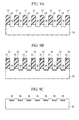
- FIGs. 1A and 1B are a plan view and a diagrammatic sectional view illustrating a structure of the carbon nanotube sheet according to the present embodiment.
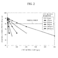
- FIG. 2 is a graph illustrating a relationship between the thermal conductivity of the carbon nanotube sheet according to the present embodiment.
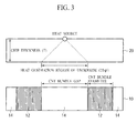
- FIG. 3 is a view explaining the gap of the carbon nanotube bundles of the carbon nanotube sheet according to the present embodiment.
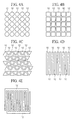
- FIGs. 4A-4E are plan views illustrating configurations of the carbon nanotube bundles of the carbon nanotube sheet according to the present embodiment.
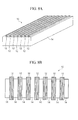
- FIGs. 5A-5E are diagrammatic sectional views illustrating the structures of the carbon nanotube sheet according to the present embodiment.
- FIGs. 6A-7D are sectional views illustrating a method of manufacturing the carbon nanotube sheet according to the present embodiment.
- the carbon nanotube sheet 10 has the structure that a plurality of carbon nanotube bundles 12 are arranged at a gap from each other, and the gaps are filled with a filling layer 14 of a resin material or another.
- each carbon nanotube bundle 12 is formed, extended perpendicularly to the surface of the sheet and contains a plurality of carbon nanotubes oriented vertically to the surface of the sheet.
- the carbon nanotube can be a single-walled carbon nanotube or a multi-walled carbon nanotube.
- the density of the carbon nanotubes contained in the carbon nanotube bundle 12 is not especially limited but can be set preferably at not less than about 1 ⁇ 10 10 tubes/cm 2 from the view point of heat radiation and electric conduction.
- the length of the carbon nanotube bundle 12 (the thickness of the sheet) is decided by applications of the carbon nanotube sheet 10. It is not especially limited but can be set preferably at a value of about 5 - 500 ⁇ m.
- gaps are formed between the carbon nanotube bundles 12, and the filling layer 14 is formed in the gaps. This is for improving the permeability of a filling material to be the filling layer 14, suppressing the configuration changes, such as horizontal falls, etc. to retain the original orientation of the carbon nanotubes (refer to the manufacturing method which will be described later).
- the gap required between the carbon nanotube bundles 12 varies depending on the viscosity, etc. of the filling material to be the filling layer 14 and cannot be unconditionally decided.
- the gap can be set at a width sufficiently larger than a gap between the carbon nanotubes forming each carbon nanotube bundle 12, preferable at a value of about 0.1 - 200 ⁇ m.
- the gap between the carbon nanotube bundles 12 is larger, the surface density of the carbon nanotubes in the sheet surface decreases, i.e., the thermal conductivity of the sheet decreases.
- the surface density of the carbon nanotubes in the sheet surface varies, also depending on a size of the carbon nanotube bundles 12. Accordingly, the gap between the carbon nanotube bundles 12 can be set suitably for a thermal conductivity required for the sheet in consideration of a size of the carbon nanotube bundles 12.
- FIG. 2 is a graph of one of the relationships between the thermal conductivity of the sheet, and the size and the gap of the carbon nanotube bundles 12.
- FIG. 2 shows the result of the calculation made for carbon nanotube bundles 12 formed in a region of the plane pattern in which the circles are arranged in the close-packed type as illustrated in FIG. 1A with the carbon nanotube density in the carbon nanotube bundle 12 being 1 ⁇ 10 11 tubes/cm 2 and the thermal conductivity of the carbon nanotube per one tube being 1000 W/m ⁇ K.
- the size of the carbon nanotube bundles (CNT bundle) 12 is a diameter of a circles in the region where the carbon nanotube bundle 12 is formed.
- the gap of the carbon nanotube bundles 12 is a minimum distance between the circles of the region where the carbon nanotube bundles 12 are formed and their adjacent circles.
- the dotted line indicates the thermal conductivity of the conventionally used indium sheet.
- the thermal conductivity of the carbon nanotube sheet 10 largely depends on the size and the gap of the carbon nanotube bundles 12 and increases as the size of the carbon nanotube bundles 12 is larger and as the gap of the carbon nanotube bundles 12 is smaller.
- the gap of the CNT bundles is not more than about 4 ⁇ m when the diameter of the CNT bundles 12 is 50 ⁇ m, at not more than about 7 ⁇ m when the diameter of the CNT bundles 12 is 100 ⁇ m, at not more than about 14 ⁇ m when the diameter of the CNT bundles 12 is 200 ⁇ m, at not more than about 36 ⁇ m when the diameter of the CNT bundles 12 is 500 ⁇ m, at not more than about 72 ⁇ m when the diameter of the CNT bundles 12 is 1000 ⁇ m, and at not more than about 151 ⁇ m when the diameter of the CNT bundles 12 is 2000 ⁇ m.
- the whole chip does not generate heat but generates heat at the hot spot (heat generation source) as the center.
- the heat generating region of the chip 10 underside when the hot spot is located near the surface of the chip 20, the heat generating region of the chip 10 underside, where heat is generated by the heat spot, is a 2T ⁇ region when the thickness of the chip 20 is T.
- the thickness of the chip 20 is 100 ⁇ m
- the heat generating region of the underside will be about 200 ⁇ m.
- the carbon nanotube bundles 12 to be the radiation path is present essentially in the 200 ⁇ m ⁇ region.
- the gap of the carbon nanotube bundles 12 is set at not more than 200 ⁇ m.
- the plane shape of the respective carbon nanotube bundles 12 is not limited to the circle illustrated in FIG. 1A .
- the plane shape of the carbon nanotube bundles 12 can be polygons other than circular, e.g., triangle, quadrangle, hexagon, etc.
- the layout of a plurality of the carbon nanotube bundles 12 is not limited to the circular close-packed layout as illustrated in FIG. 1A .
- the carbon nanotube bundles 12 may be laid out at the respective lattice points of the tetragonal lattice.
- the carbon nanotube bundles 12 of a triangular plane shape may be arranged upside down with respect to the adjacent one in each row.
- the carbon nanotube bundles 12 may be arranged in the stripe pattern.
- the carbon nanotube bundles 12 may be arranged in a comb-pattern.
- the carbon nanotube bundles 12 have the upper ends and the lower ends not covered by the filling layer 14, whereby when the carbon nanotube sheet 10 is brought into contact with a heat radiator or a heat generator, the carbon nanotube bundles 12 are in direct contact with the heat radiator or the heat generator, which can largely improve the thermal conductivity.
- the carbon nanotube also has electric conductivity, and the carbon nanotube bundles 12 have the upper ends and the lower ends exposed, which makes it possible to use the carbon nanotube bundles 12 also as interconnections passed through the sheet. That is, the carbon nanotube sheet 10 according to the present embodiment can be used not only as a thermal conductive sheet but also as the vertical interconnecting sheet.
- the height of the carbon nanotube bundles 12 and the thickness of the filling layer 14 may be the same, as illustrated in FIG. 5A .
- one ends of the carbon nanotube bundles 12 may be lower than the surface of the filling layer 14.
- one ends of the carbon nanotube bundles 12 may be higher than the surface of the filling layer 14.
- Such configurations can be respectively formed by varying the material of the filling layer 14 and forming conditions (refer to the manufacturing method described below).
- the configuration of FIG. 5B is expected to mitigate stresses exerted to the carbon nanotube bundles 12 by the filling layer 14 when the carbon nanotube sheet 10 is arranged between a heat radiator and a heat generator in press-contact therewith.
- the configuration of FIG. 5C is expected to improve the close contact of the carbon nanotube bundles 12 to the heat radiator and the heat generator to improve the thermal conductivity.
- the relationship between the height of the carbon nanotube bundles 12 and the thickness of the filling layer 14 is set suitably in accordance with applications of the carbon nanotube sheet 10 and stresses, etc. exerted to the carbon nanotube sheet 10.
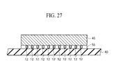
- a coating film 18 connected to the ends of the carbon nanotube bundles 12 may be provided on at least one surface of the carbon nanotube sheet 10.
- the coating film 18 is not especially limited as long as the coating film 18 is formed of a material whose thermal conductivity is higher than that of the material forming the filling layer 14.
- a material having electric conductivity e.g., a metal, an alloy or others can be used.
- the constituent material of the coating film copper (Cu), nickel (Ni), gold (Au) or others, can be used.
- the coating film 18 may not have essentially a single layer structure and may have a two-layer structure, or a three- or more-layer structure, e.g., the layer structure of titanium (Ti) and gold (Au).
- the film thickness of the coating film 18 is not especially limited.
- the film thickness of the coating film is suitably decided, depending on characteristics required of the carbon nanotube sheet 10 and a constituent material of the coating film 18.
- the coating film 18 of high thermal conductivity is provided, whereby the contact area of the carbon nanotube sheet 10 with respect to a mounted body (a heat radiator or a heat generator) can be increased with respect to the carbon nanotube sheet 10 without the coating film 18.
- a mounted body a heat radiator or a heat generator
- the thermal conductivity of the carbon nanotube sheet 10 can be increased.
- the electric conductivity can be increased.
- the coating film 18 is formed on one surface of the carbon nanotube sheet 10 illustrated in FIG. 5A , but the coating film 18 may be formed on both surfaces of the carbon nanotube sheet 10.
- the coating film 18 may be formed on one surface or both surfaces of the carbon nanotube sheet 10 illustrated in FIG. 5B or FIG. 5C .
- the constituent material of the filling layer 14 is not especially limited as long as the material has the property that the material is liquid when filling the spaces between the carbon nanotubes and can be hardened later.
- the organic filling materials acryl resin, epoxy resin, silicone resin, polyimide resin, etc. can be used.
- insulating film forming compositions by using spin coating such as SOG (Spin On Glass), etc.
- Metal materials such as indium, solder, metal pastes (e.g., silver paste), etc., can be also used.
- Conductive polymers such as polyaniline, polythiophene, etc., can be used.
- an additive may be mixed as required.
- a highly thermally conductive material or a highly electrically conductive material for example, is considered.
- a highly thermally conductive additive is mixed in the filling layer 14, whereby the thermal conductivity of a part of the filling layer 14 can be improved, and the thermal conductivity of the carbon nanotube sheet as a whole can be improved.
- a highly electrically conductive additive is mixed in the filer layer 14, whereby the electrical conductivity of a part of the filling layer 14 can be improved, and the electric conductivity of the carbon nanotube sheet 10 as a whole can be improved.
- a low thermally conductive insulating material such as an organic filling material or another, for example, is used as the filling layer 14.
- a low thermally conductive insulating material such as an organic filling material or another, for example
- carbon nanotube, a metal material, aluminum nitride, silica, alumina, graphite, fullerene or others can be used.
- highly electrically conductive material, carbon nanotube, a metal material, etc. can be used.
- the coating film 18 When the filling layer 14 is formed of a reflowable material, in addition to the effects of improving the thermal conductivity and/or the electrical conductivity of the carbon nanotube sheet 10, the coating film 18 also exhibits an effect for suppressing the carbon nanotubes of the carbon nanotube bundles 12 to loose.
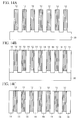
- a substrate 30 to be used as the base for forming the carbon nanotube sheet 10 is prepared ( FIG. 6A ).
- a semiconductor substrate such as a silicon substrate or another, an alumina (sapphire) substrate, an MgO substrate, a glass substrate or another can be used.
- Such substrates may have thin film formed on.
- a silicon substrate with an about 300 nm-thickness silicon oxide film formed on can be used.
- the substrate 30 is to be peeled after the carbon nanotube sheet 10 has been formed.
- the substrate 30 has at least the surface to contact the carbon nanotube sheet 10 is formed of a material which is easily peelable from the carbon nanotube sheet 10 or a material which can be selectively etched with respect to the carbon nanotube sheet 10.
- acryl resin when used as the material of the filling layer 14, a material which is less adhesive to acryl resin, e.g., silicon oxide film, silicon nitride film or another is formed, whereby the carbon nanotube sheet 10 can be easily peeled.
- the surface of the substrate 30 is formed of a material, such as silicon oxide film, silicon nitride film or another, which can be selectively etched with respect to the carbon nanotube sheet 10, whereby the film is etched off, and the carbon nanotube sheet 10 can be released from the substrate 30.
- a photoresist film 32 is formed by spin coating method ( FIG. 6B ).
- openings 34 exposing the regions for the carbon nanotube bundles 12 to be formed in are formed by photolithography ( FIG. 6C ).
- the pattern of the openings 34 is the pattern of, e.g., FIG. 1A .
- the diameter of the openings 34 (the diameter of the region for the carbon nanotube bundles 12 to be formed in) is, e.g., 100 ⁇ m, and the gap between the openings 34 (the gap between the carbon nanotube bundles 12) is, e.g., 20 ⁇ m.
- the pattern of the openings formed in the photoresist film 32 can be various patterns illustrated in, e.g., FIGs. 4A to 4E other than the pattern of FIG. 1A .
- a 2.5 nm-thickness Fe (iron) film is formed by, e.g., sputtering method to form a catalytic metal film 36 of Fe ( FIG. 6D ).
- the catalytic metal film 36 is formed on the photoresist film 32 and on the substrate 30 in the openings 34.
- Co cobalt
- Ni nickel
- Au gold
- Ag silver
- Pt platinum
- an alloy containing at least one of them can be used other than Fe.
- metal particles formed with a size controlled in advance with a DMA (Differential Mobility Analyzer) or others can be used other than the metal film. In this case as well, the metal species can be the same as that of the thin film.
- a film of Mo (molybdenum), Ti (titanium), Hf (hafnium), Zr (zirconium), Nb (niobium), V (vanadium), TaN (tantalum nitride), TiSi x (titanium silicide), Al (aluminum), Al 2 O 3 (aluminum oxide), TiO x (titanium oxide), Ta (tantalum), W (tungsten), Cu (copper), Au (gold), Pt (platinum), Pd (palladium), TiN (titanium nitride) or an alloy containing at least one of them may be formed.
- the layer structure of Fe (2.5 nm)/Al (10 nm), the layer structure of Co (2.6 nm)/TiN (5 nm), etc. can be used.
- the layer structure of, e.g., Co (average diameter: 3.8 nm)/TiN (5 nm) can be used.
- the catalytic metal film 36 on the photoresist film 32 is removed by lift-off together with the photoresist film 32 to leave the catalytic metal film 36 selectively on the substrate 30 in the regions for the carbon nanotube bundles 12 to be formed on ( FIG. 7A ).
- the catalytic metal film 36 is left selectively in the regions for the carbon nanotube bundles 12 to be formed on, but the process for selectively forming the catalytic metal film 36 is not limited to the above.
- a metal mask having openings in the regions for the carbon nanotube bundles 12 to be formed in may be used. With the surface of the substrate 30 covered by the metal mask, the catalytic metal is sputtered to thereby form the catalytic metal film 36 selectively in the regions for the carbon nanotube bundles 12 to be formed on.
- carbon nanotubes are grown with the catalytic metal film 36 as the catalyst by, e.g., hot filament CVD method.
- the conditions for growing the carbon nanotubes are, e.g., the raw material gas: the mixed gas of acetylene and argon (partial pressure ratio 1:9), the total gas pressure in the film forming chamber: 1 kPa, the hot filament temperature: 1000 °C, and the growing period of time: 20 minutes.
- the raw material gas the mixed gas of acetylene and argon (partial pressure ratio 1:9)
- the total gas pressure in the film forming chamber 1 kPa
- the hot filament temperature 1000 °C
- the growing period of time 20 minutes.
- the carbon nanotubes may be grown another film forming process, such as thermal CVD method, remote plasma CVD method or others.
- the grown carbon nanotubes may be single-walled carbon nanotubes.
- As the carbon raw material other than acetylene, hydrocarbons, such as methane, ethylene, etc., and alcohols, such as ethanol, methanol, etc., and others may be used.
- carbon nanotube bundles 12 containing a plurality of carbon nanotubes oriented in the normal direction of the substrate 30 (vertically) are selectively formed on the regions of the substrate 30, where the catalytic metal film 36 is formed ( FIG. 7B ).
- the carbon nanotube density inside the carbon nanotube bundles 12 is about 1 ⁇ 10 11 tubes/cm 2 .
- a filling material to be the filling layer 14 is applied by, e.g., spin coating method.
- the viscosity of the coating solution and the rotation number of the spin coater are suitably set so that the filling material does not cover the tops of the carbon nanotube bundles 12.
- acryl resin when acryl resin is used as the filling material, to make the height of the carbon nanotube bundles 12 and the thickness of the filling layer 14 substantially equal to each other (see FIG. 5A ), it can be realized by, e.g., applying acrylic resin of a 440 mPa ⁇ s viscosity under the conditions of 2000 rpm and 20 seconds.
- the thickness of the filling layer 14 is made smaller than the height of the carbon nanotube bundles 12 (see FIG. 5C ), it can be realized, e.g., by applying acryl resin of a 440 mPa ⁇ s viscosity under the conditions of 4000 rpm and 20 seconds. Otherwise, it can be realized by, e.g., applying acryl resin diluted to 80 wt% with an MEK (methyl ethyl ketone) solution under the conditions of 2000 rpm and 20 seconds.
- MEK methyl ethyl ketone
- the upper surfaces of the carbon nanotubes bundles 12 may be exposed by ashing method or others after the filling material has been formed, covering the tops of the carbon nanotube bundles 12 (refer to a second embodiment).
- the filling material is not especially limited as long as the filling material is liquid and then hardenable.
- the organic filling materials acryl resin, epoxy resin, silicone resin, polyimide resin, etc. can be used.
- insulating film forming compositions by using spin coating such as SOG (Spin On Glass), etc.
- Metal materials such as indium, solder, metal pastes (e.g., silver paste), etc., can be also used.
- the applied filling material In forming the filling layer 14, because of a plurality of the carbon nanotube bundles 12 formed on the substrate 30 with gaps therebetween, the applied filling material first spread on the substrate 30 along the gaps. Then, the filling material goes on permeating into the carbon nanotube bundles 12.
- the carbon nanotubes are formed on the entire surface of the substrate 30, when the filling material permeates into the carbon nanotube, the discrete carbon nanotubes coagulate with each other, and the carbon nanotubes lose the orientation they have originally retained and tend to have configuration changes, e.g., to fall horizontally.
- the filling material filled in advance between the carbon nanotube bundles 12 acts as the supporter for retaining the configuration of the carbon nanotubes when the filling material permeates into the carbon nanotube bundles 12 and prevents the configuration changes of the carbon nanotube bundles 12.
- the filling layer 14 can be formed with the orientation of the carbon nanotube bundles 12 retained.
- a gap required between the carbon nanotube bundles 12 varies, depending on a kind, viscosity, etc. of the filling material and cannot be unconditionally decided.
- the inventors of the present invention made studies and confirmed that a gap of not less than 0.1 ⁇ m can prevent the configuration change of the carbon nanotube bundles 12.
- the resin layer 14 may be formed by immersing the substrate 30 in a solution of the filling material (the so-called dip method). In this case as well, the gap provided between the carbon nanotube bundles 12 can prevent the configuration change of the carbon nanotube bundles 12.
- the filling material is hardened to form the filling layer 14 of the filling material ( FIG. 7C ).
- the filler can be hardened by light irradiation.
- a thermosetting material such as epoxy resin, silicone resin or others
- the filling material can be hardened by thermal processing.
- Epoxy resin can be thermoset, e.g., by 1 hour of heat processing of 150 °C.
- Silicone resin can be thermoset, e.g., by 1 hour of heat processing of 200 °C.
- the filling layer 14 on the carbon nanotube bundles 12 may be removed by CMP (Chemical Mechanical Polishing) or oxygen plasma ashing.
- the carbon nanotube bundles 12 and the filling layer 14 are peeled from the substrate 20, and the carbon nanotube sheet 10 is obtained ( FIG. 7D ).
- the surface of the substrate 30 being formed of a material which is able to easily peel the carbon nanotube sheet 10
- the silicon oxide film or silicon nitride film, for example is formed on the surface of the substrate 30, and the filling layer 14 is formed of acryl resin, the carbon nanotube sheet 10 can be easily peeled from the substrate 30.
- the carbon nanotube sheet 10 can be easily peeled form the substrate 30.
- the carbon nanotube sheet 10 can be peeled from the substrate 30 by removing the silicon oxide film or the silicon nitride film by wet etching using, e.g., diluted hydrofluoric acid, boiled phosphoric acid or others.
- the substrate 30 With the surface of the substrate 30 being formed of a material which can neither easily peel the carbon nanotube sheet 10 nor is selectively removed, when the substrate 30 is a sapphire substrate, and the filling layer 14 is formed of silicone-based resin, for example, a sharp cutting tool is inserted into between the substrate 30 and the carbon nanotube sheet 10 to thereby peel the carbon nanotube sheet 10 from the substrate 30.
- the carbon nanotube bundles 12 Before peeled, the carbon nanotube bundles 12 have been in direct contact with the substrate, so that the carbon nanotube bundles 12 are exposed on the peeled surface thereof on the side of the substrate 30. Accordingly, the carbon nanotube sheet 10 manufactured by the above-described manufacturing method can have both ends of the carbon nanotube bundles 12 exposed on both surfaces of the sheet.
- regions where the carbon nanotube bundles 12 are formed are relatively recessed due to the volume contraction ratio difference between the filling material and the carbon nanotubes. That is, the ends of the carbon nanotube bundles 12 on the surface of the carbon nanotube sheet 10 which has been in contact with the substrate 30 are recessed from the surface of the filling layer 14 (see FIG. 5B ). These recesses can be utilized to mitigate stresses due to thermal expansion and can play the role of supporting the adhesion.
- a coating film 18 is formed on one surface or both surfaces of the carbon nanotube sheet 10 (see FIG. 5D ).
- the coating film 18 can be formed by, e.g., sputtering method.
- the coating film 18 of the layer film of, e.g., a 10 nm-thickness titanium (Ti) film and, e.g., a 50 nm-thickness gold (Au) film can be used.
- a plurality of the carbon nanotube bundles are formed on the substrate, spaced from each other, and then the filling material is filled to form the filling layer which supports the carbon nanotube bundles, whereby the configuration change of the carbon nanotube bundles in forming the filling layer can be prevented.
- the carbon nanotube sheet including the carbon nanotube bundles oriented in the direction of thickness of the sheet can be easily formed.
- the carbon nanotube bundles can have both ends exposed in the filling layer, which can improve the thermal conductivity and the electric conductivity with respect to an object for the carbon nanotube sheet to be mounted on.
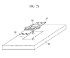
- the carbon nanotube sheet and the method of manufacturing the same according to a second embodiment will be explained with reference to FIGs. 8A to 11B .
- the same members of the present embodiment as the carbon nanotube sheet and the method of manufacturing the same according to the first embodiment illustrated in FIGs. 1A to 7D are represented by the same reference numbers not to repeat or to simplify their explanation.
- FIG. 8A is a perspective view illustrating a structure of the carbon nanotube sheet according to the present embodiment.
- FIG. 8B is a diagrammatic sectional view illustrating the structure of the carbon nanotube sheet according to the present embodiment.
- FIGs. 9A-11B are sectional views illustrating a method of manufacturing the carbon nanotube sheet according to the present embodiment.
- the carbon nanotube sheet 10 comprises carbon nanotube bundles 12 of a stripe-shaped pattern buried by a filling layer 14. As illustrated in FIG. 8B , the ends of the carbon nanotube bundles 12 are positioned higher than the surface of the filling layer 14 on both surfaces of the sheet.
- Such structure of the carbon nanotube sheet 10 permits the carbon nanotube bundles 12 to be easily and surely connected a heat radiator or a heat generator when the carbon nanotube sheet 10 is brought into contact with the heat radiator or the heat generator, whereby the thermal conductive efficiency can be largely improved.
- the carbon nanotube sheet 10 is used as a conductive sheet, the carbon nanotube sheet 10 can be easily and surely connected to other interconnection structures, whereby the contact resistance can be largely reduced.
- the projection amount of the carbon nanotube bundles 12 with respect to the filling layer 14 is sufficiently not more than about 1 ⁇ m (e.g., about 500 nm) from the viewpoint of ensuring the connection to another structure.
- the manufacturing method according to the present embodiment, which will be described later, can easily control the projection amount of the carbon nanotube bundles 12.
- the carbon nanotube bundles 12 have the ends projected with respect to the filling layer 14 on both sides of the sheet but may have the ends projected on only one side of the sheet.
- the plane pattern of the carbon nanotube bundles 12, the constituent material of the filling layer 14, the conditions for forming the carbon nanotube bundles 12 and the filling layer 14, the film thickness and other property value, etc. which are applicable to the carbon nanotube sheet 10 according to the present embodiment are the same as in carbon nanotube sheet according to the first embodiment.
- a substrate 30 to be used as the base for manufacturing the carbon nanotube sheet 10 is prepared.
- a silicon substrate with, e.g., an about 1 ⁇ m-thickness silicon oxide film formed on is used.
- a photoresist film 30 having openings 34 for exposing the regions for the carbon nanotube bundles 12 to be formed in is formed.
- the substrate 30 is anisotropically etched to form concaves 38 of an about 500 nm-depth in the surface of the substrate 30 ( FIG. 9A ).
- the concaves 38 are formed in the regions of the substrate 30, where the carbon nanotube bundles 12 are to be formed.
- the width of the concaves 38 can be, set at, e.g., 100 ⁇ m, and the gap between the concaves 38 can be set at, e.g., 20 ⁇ m.
- the width and the gap of the concaves 38 are set suitably in accordance with a thermal conductivity, etc. necessary for the carbon nanotube sheet 10.
- the depth of the concaves 38 corresponds to the projection amount of the carbon nanotube sheet 12 with respect to the filling layer 14. Accordingly, the depth of the concaves 38 is suitably set, whereby the projection amount of the carbon nanotube bundles 12 with respect to the filling layer 14 can be controlled.
- a 2.5 nm-thickness Fe (iron) film for example, is formed to form a catalytic metal film 36 of Fe ( FIG. 9B ).
- the catalytic metal film 36 is formed on the photoresist film 32 and in the concaves 38 of the substrate 30.
- the catalytic metal film 36 on the photoresist film 32 is lifted off together with the photoresist film 32 to leave the catalytic metal film 36 selectively in the concaves 38 of the substrate 30 ( FIG. 9C ).
- carbon nanotubes are grown by, e.g., hot filament CVD method.
- the carbon nanotube bundles 12 containing a plurality of carbon nanotubes oriented in the direction of the normal of the substrate 30 are selectively grown in the region of the concaves 38 ( FIG. 10A ).
- epoxy resin for example, is applied by, e.g., spin coating method, and then thermal processing of, e.g., 150 °C is made for 1 hour to cure the epoxy resin.
- thermal processing of, e.g., 150 °C is made for 1 hour to cure the epoxy resin.
- the filling layer of epoxy resin is formed ( FIG. 10B ).
- an upper part of the filling layer 14 is removed by, e.g., ashing using oxygen plasma to expose upper ends of the carbon nanotube bundles 12 ( FIG. 11A ).
- the conditions for the ashing can be, e.g., the power: 200 W and the period of time: 10 minutes.
- the upper part of the filling layer 14 may be removed by heating in an oxygen atmosphere in place of the ashing with oxygen plasma.
- the ashing selective ratio of the filling layer 14 to the carbon nanotube bundles 12 is about 1.26. Accordingly, the upper part of the filling layer 14 is ashed, whereby the upper ends of the carbon nanotube bundles 12 can be higher than the surface of the filling layer 14.
- the etching rate of the filling layer 14 is suitably set, whereby the projection amount of the carbon nanotube bundles 12 with respect to the filling layer 14 can be controlled.
- the upper ends of the carbon nanotube bundles 12 may be exposed by, e.g., chemical mechanical polishing.
- the filling layer 14 is formed, covering the upper ends of the carbon nanotube bundles 12, but as in the first embodiment, the upper ends of the carbon nanotube bundles 12 may be exposed by controlling the application conditions of the filling layer 14. In this case, the step of FIG. 11A is not required. It is sufficient that the upper ends of the carbon nanotube bundles 12 are exposed in the step of FIG. 11A , When the upper ends of the carbon nanotube bundles 12 of only one surface of the sheet is projected.
- the carbon nanotube bundles 12 and the resin layer 14 are peeled from the substrate 30, and the carbon nanotube sheet 10 having the carbon nanotube bundles 12 projected with respect to the surface of the filling layer 12 on both surfaces of the sheet is formed ( FIG. 11B ).
- the carbon nanotube sheet having the ends of the carbon nanotube bundles projected with respect to the surface of the filling layer can be easily manufactured.
- Such carbon nanotube sheet can further improve the thermal conductivity and the electric conductivity with respect to an object to be mounted on.
- the carbon nanotube sheet and the method of manufacturing the same according to a third embodiment will be explained with reference to FIGs. 12A to 14C .
- the same members of the present embodiment as those of the carbon nanotube sheet and the method of manufacturing the same according to the first and the second embodiments illustrated in FIGs. 1A to 11B are represented by the same reference numbers not to repeat or to simplify their explanation.
- FIG. 12A is a perspective view illustrating a structure of the carbon nanotube sheet according to the present embodiment.
- FIG. 12B is a diagrammatic sectional view illustrating the structure of the carbon nanotube sheet according to the present embodiment.
- FIGs. 13A-13C and 14A-14C are sectional views illustrating a method of manufacturing the carbon nanotube sheet according to the present embodiment.
- the carbon nanotube sheet 10 comprises carbon nanotube bundles 12 of a stripe-shaped pattern buried by a filling layer 14.
- the ends of the carbon nanotube sheet 12 are lower than the surface of the filling layer 14 on one surface of the sheet. The ends of the carbon nanotube bundles 12 are not covered by the filling layer 14.
- Such structure of the carbon nanotube sheet 10 permits the carbon nanotube sheet 10 to be connected directly to a heat radiator or a heat generator when the carbon nanotube sheet 10 is brought into contact with the heat radiator or the heat generator, whereby the thermal conductive efficiency can be largely improved.
- the carbon nanotube sheet 10 can be connected directly to other interconnection structures, and the contact resistance can be largely decreased.
- the carbon nanotube sheet 10 is disposed between the heat radiator and the heat generator in close contact, stresses to be exerted to the carbon nanotube bundles 12 could be mitigated by the filling layer 14.
- the plane pattern of the carbon nanotube bundles 12, the constituent material of the filling layer 14, the conditions for forming the carbon nanotube bundles 12 and the filling layer 14, the film thickness and other property values, etc. which are applicable to the carbon nanotube sheet 10 according to the present embodiment are the same as those of the carbon nanotube sheet according to the first embodiment.
- a substrate 30 as the base for forming the carbon nanotube sheet 10 is prepared.
- a silicon substrate with an about 1 ⁇ m-thickness silicon oxide film formed on is used.
- a 2.5 nm-thickness Fe (iron) film is formed over the substrate 30 by, e.g., sputtering method to form a catalytic metal film 36 of Fe ( FIG. 13A ).
- a photoresist film 32 covering the regions for the carbon nanotube bundles 12 to be formed in and exposing the rest region is formed by photolithography.
- the catalytic metal film 36 and the substrate 30 are anisotropically etched to form the concaves 38 of an about 500 nm-depth in the surface of the substrate 30 ( FIG. 13B ).
- the concaves 38 are formed in the regions other than the regions for the carbon nanotube bundles 12 to be formed on.
- the width of the concaves 38 can be set at, e.g., 20 ⁇ m, and the gap of the concaves 38 can be set at, e.g., 100 ⁇ m.
- the width and the gap of the concaves 38 are set suitably in accordance with a thermal conductivity, etc. required for the carbon nanotube sheet 10.
- the photoresist film 32 is removed ( FIG. 13C ).
- carbon nanotubes are grown by, e.g., hot filament CVD method.
- the carbon nanotube bundles 12 containing a plurality of the carbon nanotubes oriented in the direction of the normal of the substrate 30 are formed selectively on the regions of the substrate other than the regions for the concaves 38 to be formed in ( FIG. 14A ).
- epoxy resin for example
- thermal processing e.g., of 150 °C is made for 1 hour to harden the epoxy resin.
- the filling layer 14 of epoxy resin is formed.
- the filling layer 14 is formed also in the concaves 38 of the substrate 30 ( FIG. 14B ).
- the surfaces of the carbon nanotube bundles 12 and the surface of the filling layer 14 are flash with each other, but the ends of the carbon nanotube bundles 12 may be projected with respect to the surface of the filling layer 14.
- the process for forming such configuration is the same as in the first and the second embodiments.
- the carbon nanotube bundles 12 and the resin layer 14 are peeled from the substrate 30, and the carbon nanotube sheet 10 having the ends of the carbon nanotube bundles 12 positioned on one surface of the sheet lower than the surface of the filling layer 14 is obtained ( FIG. 14C ).
- the carbon nanotube sheet comprising the carbon nanotube bundles having the ends recessed with respect to the surface of the filling layer can be easily formed.
- stresses exerted to the carbon nanotube bundles can be mitigated by the filling layer.
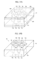
- the carbon nanotube sheet and the method of manufacturing the same according to a fourth embodiment will be explained with reference to FIGs. 15A to 19B .
- the same members of the present embodiment as those of the carbon nanotube sheet and the method of manufacturing the same according to the first to the third embodiments illustrated in FIGs. 1A to 14C are represented by the same reference numbers not to repeat or to simplify their explanation.
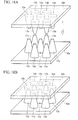
- FIG. 15A is a plan view illustrating a structure of the carbon nanotube sheet according to the present embodiment.
- FIG. 15B is a diagrammatic sectional view illustrating the structure of the carbon nanotube sheet according to the present embodiment.
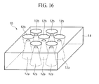
- FIG. 16 is a perspective view illustrating the structure of the carbon nanotube sheet according to the present embodiment.
- FIGs.17A-17C, 18A-18B and 19A-19B are views illustrating a method of manufacturing the carbon nanotube sheet according to the present embodiment.
- the carbon nanotube sheet 10 according to the present embodiment is the same as the carbon nanotube sheet according to the first to the third embodiments in that a plurality of carbon nanotube bundles 12a, 12b are arranged spaced from each other with a gap, and a filling layer 14 of a resin material or others is filled in the gaps.
- each of the plural carbon nanotube bundles 12 has a tapered configuration having the diameter of one end smaller than the diameter of the other end.
- Each of the carbon nanotube bundles 12a, 12b has the tapered configurations defined by the gaps between the carbon nanotubes gradually decreased from the end of the larger diameter toward the end of the smaller diameter. In other words, the number of the carbon nanotubes does not substantially change between the side of the larger diameter of the carbon nanotube bundles 12a, 12b and the side of the smaller diameter of the carbon nanotube bundles 12a, 12b.
- the plurality of carbon nanotube bundles 12 are divided in the carbon nanotube bundles 12a having a smaller diameter on one surface of the carbon nanotube sheet 10, and the carbon nanotube bundles 12b having a smaller diameter on the other surface of the carbon nanotube sheet 10. As exemplified in FIGs. 15B and 16 , the carbon nanotube bundles 12a and the carbon nanotube bundles 12b are arranged alternately so as to engage with each other and fill the gaps.
- the carbon nanotube sheet 10 is viewed from one surface of the carbon nanotube sheet 10, as exemplified in FIG. 15A and FIG. 15B , the smaller-diameter ends of the carbon nanotube bundles 12a and the large-diameter ends of the carbon nanotube bundles 12b are exposed. As illustrated in FIG. 15B , on the other surface of carbon nanotube sheet 10, the large-diameter ends of the carbon nanotube bundles 12a and the smaller-diameter ends of the carbon nanotube bundles 12b are exposed.
- Such carbon nanotube bundles 12a, 12b are used to thereby increase the number of the carbon nanotubes per a unit area of the carbon nanotube sheet 10 (the surface density of the carbon nanotubes).
- the diameters of the large-diameter ends of the carbon nanotube bundles 12b and the arrangement gap thereof are the same as those of the carbon nanotube bundles 12 of the carbon nanotube sheet according to the first embodiment illustrated in FIG. 1A
- the same number of the carbon nanotube bundles 12a can be further arranged in the gaps between the carbon nanotube bundles 12b. That is, the surface density of the carbon nanotubes of the carbon nanotube sheet 10 can be doubled. Thus, the thermal conductivity and electric conductivity of the carbon nanotube sheet 10 can be drastically increased.
- a catalytic metal film 36 is formed on a substrate 30a in the regions for the carbon nanotube bundles 12 to be formed in ( FIG. 17A ).
- the substrate 30a is the same as the substrate 30 of the first to the third embodiments.
- carbon nanotubes are grown with the catalytic metal film 36 as the catalyst by, e.g., hot filament CVD method.
- the carbon nanotube bundles 12 of a plurality of carbon nanotubes oriented in the normal direction of the substrate 30a are formed selectively over the substrate 30a in the regions where the catalytic metal film 36 has been formed ( FIG. 17B ).
- the substrate 30a with the carbon nanotube bundles 12 formed on is immersed in a liquid and dried.
- the carbon nanotube bundles 12 are immersed in the liquid, the gaps between the carbon nanotubes are filled with the liquid.
- attractive forces work due to the surface tension between the adjacent carbon nanotubes.
- the ends of the carbon nanotube bundles 12, which are on the side of the substrate 30a are retained by the substrate 30a, and the gaps between the carbon nanotubes are not changed.
- the forward ends of the carbon nanotubes being not secured, the gaps between the carbon nanotubes goes on gradually decreasing.
- the carbon nanotube bundle 12 after the liquid has been dried become the tapered nanotube bundles 12a having the diameter of the forward ends smaller than the diameter of the ends on the side of the substrate 30a ( FIG. 17C ).
- the liquid to be used in tapering the carbon nanotube bundles 12 is not especially limited as long as the liquid has good wetting to the carbon nanotubes and is evaporable at a temperature which is not so high as to break the carbon nanotubes.
- an organic chemical liquid such as alcohol-based chemical liquid, ketone-based chemical liquid or others can be used.
- the alcohol-based chemical liquid is not especially limited and can be, e.g., isopropyl alcohol, ethanol, methanol, etc.
- the ketone-based chemical liquid is not especially limited and can be, e.g., acetone, methyl ethyl ketone, methyl isobutyl ketone, etc.
- the tapered carbon nanotube bundles 12b are formed on a substrate 30b.
- the substrate 30a and the substrate 30b are bonded with each other with the surface of the substrate 30a, where the carbon nanotube bundles 12a are formed, and the surface of the substrate 30b, where the carbon nanotube bundles 12b are formed opposed to each other ( FIGs. 18A and 18B ).
- the carbon nanotube bundles 12a, 12b are laid out alternately so as to engage with each other and fill the gaps, whereby the carbon nanotube bundles 12a fill the gaps between the carbon nanotube bundles 12b, and the carbon nanotube bundles 12b fill the gaps between the carbon nanotube bundles 12a.
- the forward ends of the carbon nanotube bundles 12a contacts the surface of the substrate 30b, and the forward ends of the carbon nanotube bundles 12b contact the surface of the substrate 30a.
- the layout regions of the carbon nanotube bundles 12a, 12b are not limited to those of the present embodiment as long as the layout regions can mutually fill their gaps and can be suitably changed.
- the shape and the area of the regions for the carbon nanotube bundles 12a to be formed in and the shape and the area of the regions for the carbon nanotube bundles 12b to be formed in may be different from each other, and the layout of the carbon nanotube bundles 12a and that of the carbon nanotube bundles 12b may be different from each other.
- a filling material to be the filling layer 14 is filled between the substrate 30a and the substrate 30b, and the filling layer 14 is filled between the carbon nanotube bundles 12a, 12b ( FIG. 19A ).
- the ends of the carbon nanotube bundles 12a, 12b, which are in direct contact with the substrates 30a, 30b, are not covered by the filling layer 14.
- the effect of preventing the cohesion of the carbon nanotubes is the same as in the first embodiment.
- the carbon nanotube bundles 12a, 12b, and the filling layer 14 are peeled from the substrates 30a. 30b, and the carbon nanotube sheet 10 is obtained ( FIG. 19B ).
- the filling layer 14 is subjected to etching-back, etc. to project the ends of the carbon nanotube bundles 12a, 12b from the surface of the filling layer 14.
- the carbon nanotube sheet including the carbon nanotube bundles having a smaller diameter on one surface and the carbon nanotube bundles having a smaller diameter on the other surface is formed, whereby the surface density of the carbon nanotubes can be drastically increased.
- the thermal conductivity and/or the electrical conductivity of the carbon nanotube sheet can be drastically improved.
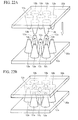
- the carbon nanotube sheet and the method of manufacturing the same according to a fifth embodiment will be explained with reference to FIGs. 20 to 22B .
- the same members of the present embodiment as those of the carbon nanotube sheet and the method of manufacturing the same according to the first to the fourth embodiments illustrated in FIGs. 1A to 19B are represented by the same reference numbers not to repeat or to simplify their explanation.
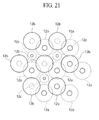
- FIG. 20 is a plan view illustrating the structure of the carbon nanotube sheet according to the fourth embodiment.
- FIG. 21 is a plan view illustrating a structure of the carbon nanotube sheet according to the present embodiment.
- FIGs. 22A-22B are views illustrating the method of manufacturing the carbon nanotube sheet according to the present embodiment.
- the two substrates 30a, 30b having the circular regions for the carbon nanotube bundles 12a, 12b formed in the close-packed type arrangement are bonded to each other to thereby improve the surface density of the carbon nanotubes.
- the plane layout of the carbon nanotube bundles 12a, 12b after bonded has regions 16 where the carbon nanotube bundles 12a, 12b are not arranged. More carbon nanotube bundles are arranged in these regions 16, whereby the surface density of the carbon nanotubes can be further improved.
- FIG. 21 illustrates the plane layout of the carbon nanotube bundles 12a, 12b and carbon nanotube bundles 12c arranged further in the regions 16 of the carbon nanotube sheet according to the present embodiment.
- the diameter of the carbon nanotube bundles corresponds to the areas of the regions 16 and is different from the diameters of the carbon nanotube bundles 12a, 12b.
- the surplus gaps which cannot be filled by the carbon nanotube bundles 12a, 12b are filled by the carbon nanotube bundles 12c, whereby the surface density of the carbon nanotubes can be further improved, which leads to the improvement of the thermal conductivity and electric conductivity of the carbon nanotube sheet.
- the carbon nanotube bundles 12c can be formed on the substrate side 30a concurrently with forming the carbon nanotube bundles 12a as exemplified in FIGs. 22A and 22B . Otherwise, all the carbon nanotube bundles 12c may be formed on the substrate 30b side, or the carbon nanotube bundles 12c may be formed on the substrate 30a side and the substrate 30b side.
- the present embodiment is explained by means of the carbon nanotube sheet according to the fourth embodiment, in which the regions for the carbon nanotube bundles 12a, 12b to be formed in are close-packed type arrangement, but the layout the method according to the present embodiment is applicable to is not limited to this.
- the carbon nanotube bundles 12c may be additionally arranged so as to fill the gaps.
- the carbon nanotube bundles for filling surplus gaps are arranged in addition to the carbon nanotube bundles having a smaller diameter on the side of one surface and the carbon nanotube bundles having a smaller diameter on the side of the other surface, whereby the surface density of the carbon nanotubes can be further increased.
- the thermal conductivity and/or the electrical conductivity of the carbon nanotube sheet can be drastically improved.
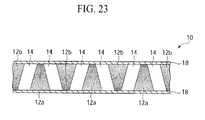
- the carbon nanotube sheet and the method of manufacturing the same according to a sixth embodiment will be explained with reference to FIG. 23 .
- the same members of the present embodiment as those of the carbon nanotube sheet and the method of manufacturing the same according to the first to the fifth embodiments illustrated in FIGs. 1A to 22B are represented by the same reference numbers not to repeat or to simplify their explanation.
- FIG. 23 is a diagrammatic sectional view illustrating a structure of the carbon nanotube sheet according to the present embodiment.
- the carbon nanotube sheet 10 according to the present embodiment is the same as the carbon nanotube sheet according to the fourth and the fifth embodiments in that the tapered carbon nanotube bundles 12a, 12b are formed in the filling layer 14.
- the carbon nanotube sheet 10 further includes coating film 18 on both surfaces thereof, connected to the ends of the carbon nanotube bundles 12a, 12b.
- the coating film 18 provided on both surfaces of the sheet is not especially limited as long as the coating film 18 is formed of a material whose thermal conductivity is higher than that of the material forming the filling layer 14.
- a material having electric conductivity e.g., a metal, an alloy or others can be used.
- the constituent material of the coating film copper (Cu), nickel (Ni), gold (Au) or others, can be used.
- the coating film 18 may not have essentially a single layer structure and may have a two-layer structure, or a three- or more-layer structure, e.g., the layer structure of titanium (Ti) and gold (Au).
- the film thickness of the coating film 18 is not especially limited.
- the film thickness of the coating film 18 is suitably decided, depending on characteristics required of the carbon nanotube sheet 10 and a constituent material of the coating film 18.
- the coating film 18 of high thermal conductivity is provided, whereby the contact area of the carbon nanotube sheet 10 with respect to a mounted body (a radiator or a heater) can be increased with respect to the carbon nanotube sheet 10 without the coating film 18.
- a mounted body a radiator or a heater
- the thermal contact resistance between the carbon nanotube bundles 12a, 12b and a mounted body is deceased, and the thermal conductivity of the carbon nanotube sheet 10 can be increased.
- the electric conductivity can be increased.
- the coating film 18 can be formed by, e.g., sputtering method after the step illustrated in FIG. 19B of the method of manufacturing the carbon nanotube sheet according to, e.g., the fourth embodiment.
- the coating film 18 of the layer film of, e.g., a 10 nm-thickness titanium (Ti) film and, e.g., a 50 nm-thickness gold (Au) film can be used.
- the coating film of a high thermal conductive material is formed on both surfaces of the sheet in contact with the ends of the carbon nanotube bundles, whereby the thermal contact resistance and the contact resistance between the sheet and a mounted body can be drastically decreased.
- the thermal conductivity and the electric conductivity of the carbon nanotube sheet can be improved.
- the carbon nanotube sheet and the method of manufacturing the same according to a seventh embodiment will be explained with reference to FIGs. 24 to 25D .
- the same members of the present embodiment as those of the carbon nanotube sheet and the method of manufacturing the same according to the first to the sixth embodiments illustrated in FIGs. 1A to 23 are represented by the same reference numbers not to repeat or to simplify their explanation.
- FIG. 24 is a diagrammatic sectional view illustrating a structure of the carbon nanotube sheet according to the present embodiment.
- FIGs. 25A-25D are views illustrating a method of manufacturing the carbon nanotube sheet according to the present embodiment.
- the carbon nanotube sheet 10 according to the present embodiment is the same as the carbon nanotube sheet according to the fourth and the fifth embodiments in that the tapered carbon nanotube bundles 12a, 12b are formed in the filling layer 14.
- the carbon nanotube sheet 10 according to the present embodiment further includes a coating film 18a formed along the surfaces of the carbon nanotube bundles 12a, a coating film 18b formed along the surfaces of the carbon nanotube bundles 12b, a coating film 18c formed entirely on one surface of the sheet and a coating film 18d formed entirely on the other surface of the sheet.
- the coating films 18a, 18b, 18c, 18d are formed of a material whose thermal conductivity is higher than the constituent material of the filling layer 14, as is the coating film 18 of the sixth embodiment.
- the coating films are formed of an electric conductive material.
- the coating films 18a, 18b, 18c, 18d are provided, whereby the contact area of the carbon nanotube sheet 10 with respect to a mounted body can be increased in comparison with that of the carbon nanotube sheet 10 without the coating film 18.
- the thermal contact resistance between the carbon nanotube bundles 12a, 12b with the mounted body is decreased, ad the thermal conductivity of the carbon nanotube sheet 10 can be increased.
- the electric conductivity can be increased.
- the tapered carbon nanotube bundles 12a are formed over the substrate 30a ( FIG. 25A ).
- a 10 nm-thickness titanium (Ti) film, for example, and a 50 nm-thickness gold (Au) film, for example, are deposited on the entire surface by, e.g., sputtering method to form the coating film 18a of the layer film of Au/Ti ( FIG. 25B ).
- tapered carbon nanotube bundles 12b and the coating film 18b are formed.
- the substrate 30a and the substrate 30b are bonded to each other ( FIG. 25C ).
- a pressure is applied to the substrate 30a and the substrate 30b while heating the substrates, whereby the coating films 18a, 18b can be hot-press bonded with each other at the upper ends of the carbon nanotube bundles 12a, 12b, and the connection between the coating films 18a, 18b can be ensured.
- the filling material to be the filling layer 14 is buried by potting method between the substrate 30a and the substrate 30b to thereby fill the filling layer 14 between the carbon nanotube bundles 12a, 12b.
- the ends of the carbon nanotube bundles 12a, 12b, which are in direct contact with the substrates 30a, 30b, are never coated with the filling layer 14.
- the effect of preventing the cohesion of the carbon nanotubes is the same as in the first embodiment.
- the substrate 30a, 30b are peeled.
- a 10 nm-thickness titanium (Ti) film, for example, and a 50 nm-thickness gold (Au) film, for example, are deposited on both surfaces of the sheet by, e.g., sputtering method.
- the coating films 18c, 18d of the layer film of Au/Ti are formed ( FIG. 25D ).
- the coating films of a material of high thermal conductivity are formed in contact with the ends of the carbon nanotube bundles, whereby the thermal contact resistance and the electric contact resistance between the sheet and a mounted body can be drastically decreased.
- the thermal conductivity and electric conductivity of the carbon nanotube sheet can be improved.
- the electronic instrument according to a eighth embodiment will be explained with reference to FIG. 26 .
- FIG. 26 is a diagrammatic sectional view illustrating a structure of the electronic instrument according to the present embodiment.
- a semiconductor element 46 such as a CPU, is mounted over the circuit board 40 of, e.g., a multi-level interconnection substrate.
- the semiconductor element 46 is electrically connected to the circuit board 40, and an underfill 44 is filled between the circuit board 40 and the semiconductor element 46.
- a heat spreader 50 for diffusing heat from the semiconductor element 46 is formed, covering the semiconductor element 46. Between the semiconductor element 46 and the heat spreader 50, the carbon nanotube sheet 52 is formed.
- a heat sink 54 for radiating heat conducted to the heat spreader is formed. Between the heat spreader 50 and the heat sink 54, the carbon nanotube sheet 52 is formed.
- the carbon nanotube sheets 48, 52 are disposed respectively between the semiconductor element 46 and the heat spreader 50 and between the heat spreader 50 and the heat sink 54.
- the disclosed carbon nanotube sheets have the carbon nanotube bundles 12 oriented vertically to the surface of the sheet, and has very high vertical thermal conductivity.
- the disclosed carbon nanotube sheets are used as the thermal conductive sheets formed between the semiconductor element 46 and the heat spreader 50 and between the heat spreader 50 and the heat sink 54, whereby the heat generated by the semiconductor element 46 can be conducted effectively to the heat spreader 50 and the heat sink 54, and the heat radiating efficiency can be improved.
- the reliability of the electronic instrument can be improved.
- the carbon nanotube sheet comprising the carbon nanotube bundles oriented in the direction of thickness of the sheet is disposed between the semiconductor element and the heat spreader and between the heat spreader and heat sink, whereby the thermal conductivity between them can be large improved.
- the heat radiating efficiency of radiating the heat generated by the semiconductor element can be improved, and the reliability of the electronic instrument can be improved.
- the electronic instrument according to a ninth embodiment will be explained with reference to FIG. 27 .
- FIG. 27 is a diagrammatic sectional view illustrating a structure of the electronic instrument according to the present embodiment.
- a semiconductor element 46 of, e.g., a CPU is mounted over the circuit board 40 of, e.g., a multi-level interconnection substrate. Between the circuit board 40 and the semiconductor element 46, the carbon nanotube sheet 56 is formed. The circuit board 40 and the semiconductor element 46 are electrically connected to each other via the carbon nanotube bundles 12 of the carbon nanotube sheet 56.
- the carbon nanotube sheet 56 is disposed between the circuit board 40 and the semiconductor element 46.
- the disclosed carbon nanotube sheets include the carbon nanotube bundles 12 oriented vertical to the film surface of the sheet and having the ends thereof exposed on both surfaces of the sheet.
- the carbon nanotube is also an electric conductor which is used as an interconnecting material.
- the disclosed carbon nanotube sheets are used as the vertical interconnecting sheet formed between the circuit board 40 and the semiconductor element 46, whereby the circuit board 40 and the semiconductor device 46 can be electrically connected to each other.
- the disclosed carbon nanotube sheet having the carbon nanotube bundles oriented in the direction of film thickness of the sheet is disposed between the circuit board and the semiconductor element, whereby both can be electrically connected to each other.
- the electronic instrument according to a tenth embodiment will be explained with reference to FIG. 28 .
- FIG. 28 is a diagrammatic sectional view illustrating a structure of the electronic instrument according to the present embodiment.
- an HPA (High Power Amplifier) 60 used in radio communication stations is incorporated in a package 62 and is connected to a heat sink 64 on the underside of the package 62. Heat generated by the HPA 60 is radiated to the heat sink 64 through the underside of the package 62.
- Package 62 is also used as the electric ground and must be electrically connected to the heat sink 64. For the connection between the package 62 and the heat sink 64, it is preferable that a material having a good electric and thermal conductivity is used.
- the carbon nanotube sheet 66 is used, whereby the package 62 and the heat sink 64 can be electrically connected to each other. Heat generated by the HPA 60 can be efficiently conducted to the heat sink 64, whereby the heat radiating efficiency can be increased. Thus, the reliability of the electronic instrument can be improved.
- the carbon nanotube sheet having the carbon nanotube bundles oriented in the direction of film thickness of the sheet is disposed between the package of the HPA and the heat sink, whereby the thermal conductivity between them can be largely increased.
- the thermal conductive efficiency of the heat generated by the HPA can be increased.
- the HPA and the heat sink as the ground can be also electrically connected to each other.
- the sheet structure using the plurality of bundles of linear structures of carbon atoms the carbon nanotube sheet using the plurality of carbon nanotube bundles are disclosed, but the sheet structure using the plurality of bundles of linear structures of carbon atoms is not limited to this.
- the linear structures of carbon atoms are applicable widely to the sheet structure.
- the linear structures of carbon atoms are, other than the carbon nanotubes, carbon nanowires, carbon rods, carbon fibers. These linear structures are different from the carbon nanotubes in size but are the same as the carbon nanotubes. These linear structures are also applicable to the sheet structure.
- two substrates with the tapered carbon nanotube bundles formed on are bonded to each other to form the carbon nanotube sheet, but it is not essentially necessary that the carbon nanotube bundles 12a, 12b are tapered.
- the carbon nanotube bundles are tapered so as to improve the surface density of the carbon nanotube.
- the carbon nanotube bundles 12a, 12b are tapered.
- the both of carbon nanotube bundles 12a, 12b are tapered.
- One of the carbon nanotube bundles 12a and the carbon nanotube bundles 12b may be tapered.
- the coating film having the thermal conductivity higher than the filling material is formed on the surfaces of the carbon nanotube sheet according to the fourth embodiment.
- the coating film may be also formed on the surfaces of the carbon nanotube sheets according to the first to the third embodiments.
- the uses of the carbon nanotube sheet described in the above embodiments are not essential.
- the disclosed carbon nanotube sheets are applicable, as the thermal conductive sheet, to, e.g., radiation sheets of CPUs, HPSs for radio communication stations, HPAs for radio communication terminals, high power switches for electric cars, servers, personal computers, etc.
- the high allowable current density of the carbon nanotube sheet can be utilized to be applied to the vertical interconnecting sheets and various applications using the vertical interconnecting sheets.
Abstract
Description
- The present invention relates to a sheet structure and a method of manufacturing the same, more specifically, a sheet structure comprising a linear structure of carbon atoms oriented vertical to the sheet surface and its manufacturing method, and an electronic instrument using such a sheet structure.
- The electronic parts used in the CPUs (Central Processing Units), etc. of servers, personal computers, etc. are needed to have high radiation efficiency of heat generated by semiconductor elements. For the effective radiation of the heat generated in the semiconductor elements, the structure that a heat spreader made of a material of a high specific thermal conductivity, such as copper or another, is disposed over the semiconductor element with a thermal conductive sheet, such as indium sheet or another, disposed immediately above the semiconductor element interposed therebetween.
- However, due to the recent large increase in demand for rare metals, the price of indium has gone up, and substitute materials which are less expensive than indium are desired. In terms of the physical properties, it cannot be said that the specific thermal conductivity of indium (50 W/m·K) is high. To more effectively radiate the heat generated by the semiconductor elements, materials of higher thermal conductivities are desired.
- In such background, as a material whose thermal conductivity is higher than indium, the linear structure of carbon atoms, which is typically the carbon nanotube, is noted. The carbon nanotube not only has a very high thermal conductivity (1500 W/m·K) but also is superior in flexibility and heat resistance, and has high potential as a heat radiation material.
- As a thermal conductive sheet using carbon nanotubes, a thermal conductive sheet including carbon nanotubes dispersed in a resin, a thermal conductive sheet including carbon nanotube bundles orientationally grown on a substrate, which are buried with a resin, etc. are proposed.
- However, in the proposed thermal conductive sheets, the higher thermal conductivity of the carbon nanotube cannot be sufficiently utilized.
- It is desirable to provide a sheet structure of a very high thermal conductivity and electric conductivity, which uses a linear structure of carbon atoms and its manufacturing method, and an electronic instrument using the sheet structure.
- According to an embodiment of a first aspect of the present invention, there is provided a sheet structure having: a plurality of linear structure bundles each of which has a plurality of linear structures of carbon atoms arranged, spaced from each other at a first gap and which are arranged at a second gap which is larger than the first gap; and a filling layer filled in the first gap and the second gap and supporting the plurality of linear structure bundles.
- According to an embodiment of a second aspect of the present invention, there is provided a sheet structure having: a plurality of linear structure bundles each of which has a plurality of linear structures of carbon atoms arranged, spaced from each other at a first gap and which are arranged at a second gap which is larger than the first gap; and a filling layer filled in the first gap and the second gap and supporting the plurality of linear structure bundles, the plurality of linear structure bundles having those of a first group which are tapered with ends on one surface being smaller than ends on the other surface and those of a second group which are tapered with ends on said other surface being smaller than ends of said one surface.
- According to an embodiment of a third aspect of the present invention, there is provided an electronic instrument having: a sheet structure having: a plurality of linear structure bundles each of which has a plurality of linear structures of carbon atoms arranged, spaced from each other at a first gap and which are arranged at a second gap which is larger than the first gap; and a filling layer filled in the first gap and the second gap and supporting the plurality of linear structure bundles.
- According to an embodiment of a fourth aspect of the present invention, there is provided a method of manufacturing a sheet structure having: forming a catalytic metal film in a plurality of regions of a substrate, which are spaced from each other; forming a plurality of linear structure bundles having a plurality of linear structures of carbon atoms in the respective plurality of regions by growing liner structures of carbon atoms with the catalytic metal film as a catalyst; filling a filling material between the linear structure bundles and between the line structures to form a filling layer of the filling material; and removing the substrate.
- According to an embodiment of a fifth aspect of the present invention, there is provided a method of manufacturing a sheet structure having: forming on a first substrate first linear structure bundles in respective plural regions spaced from each other; forming on a second substrate second linear structure bundles in respective plural regions spaced from each other; bonding the first substrate and the second substrate to each other with a surface of the first substrate with the first linear structure bundles formed on and a surface of the second substrate with the second linear structure bundles formed on opposed to each other to thereby engage the first linear structure bundles and the second linear structure bundles with each other and to fill gaps; filling a filling material between the first linear structure bundles and the second linear structure bundles and between the linear structures to thereby form a filling layer; and removing the first substrate and the second substrate.
- Advantages of embodiments of the invention will be set forth in the description which follows, and in part will be apparent from the description, or may be learned by practice of the invention. Advantages of embodiments of the invention may be realized and attained by means of the elements and combinations particularly pointed out in the appended claims.
- It is to be understood that both the foregoing general description and the following detailed description are exemplary and explanatory only and are not restrictive of the invention, as claimed.
-
-
FIG. 1A is a plan view illustrating a structure of the carbon nanotube sheet according to a first embodiment of the present invention; -
FIG. 1B is a diagrammatic sectional view illustrating the structure of the carbon nanotube sheet according to the first embodiment of the present invention; -
FIG. 2 is a graph illustrating a relationship between the thermal conductivity of the carbon nanotube sheet according to the first embodiment of the present invention and the gap of the carbon nanotube bundles; -
FIG. 3 is a view explaining the gap of the carbon nanotube bundles of the carbon nanotube sheet according to the first embodiment of the present invention; -
FIGs. 4A-4E are plan views illustrating configurations of the carbon nanotube bundles of the carbon nanotube sheet according to the first embodiment of the present invention; -
FIGs. 5A-5E are diagrammatic sectional views illustrating structures of the carbon nanotube sheet according to the first embodiment of the present invention; -
FIGs. 6A-6D and 7A-7D are sectional views illustrating a method of manufacturing the carbon nanotube sheet according to the first embodiment of the present invention; -
FIG. 8A is a perspective view illustrating a structure of the carbon nanotube sheet according to a second embodiment of the present invention; -
FIG. 8B is a diagrammatic sectional view illustrating the structure of the carbon nanotube sheet according to the second embodiment of the present invention; -
FIGs. 9A-9C, 10A-10B and 11A-11B are sectional views illustrating a method of manufacturing the carbon nanotube sheet according to the second embodiment of the present invention; -
FIG. 12A is a perspective view illustrating a structure of the carbon nanotube sheet according to a third embodiment of the present invention; -
FIG. 12B is a diagrammatic sectional view illustrating the structure of the carbon nanotube sheet according to the third embodiment of the present invention; -
FIGs. 13A-13C and 14A-14C are sectional views illustrating a method of manufacturing the carbon nanotube sheet according to the third embodiment of the present invention; -
FIG. 15A is a plan view illustrating a structure of the carbon nanotube sheet according to a fourth embodiment of the present invention; -
FIG. 15B is a diagrammatic sectional view illustrating the structure of the carbon nanotube sheet according to the fourth embodiment of the present invention; -
FIG. 16 is a perspective view illustrating the structure of the carbon nanotube sheet according to the fourth embodiment of the present invention; -
FIGs. 17A-17C, 18A-18B and 19A-19B are views illustrating a method of manufacturing the carbon nanotube sheet according to the fourth embodiment of the present invention; -
FIG. 20 is a plan view illustrating the structure of the carbon nanotube sheet according to the fourth embodiment of the present invention; -
FIG. 21 is a plan view illustrating a structure of the carbon nanotube sheet according to a fifth embodiment of the present invention; -
FIGs. 22A-22B are views illustrating a method of manufacturing the carbon nanotube sheet according to the fifth embodiment of the present invention; -
FIG. 23 is a diagrammatic sectional view illustrating a structure of the carbon nanotube sheet according to a sixth embodiment of the present invention; -
FIG. 24 is a diagrammatic sectional view illustrating a structure of the carbon nanotube sheet according to a seventh embodiment of the present invention; -
FIGs. 25A-25D are views illustrating a method of manufacturing the carbon nanotube sheet according to the seventh embodiment of the present invention; -
FIG. 26 is a diagrammatic sectional view illustrating a structure of the electronic instrument according to an eighth embodiment of the present invention. -
FIG. 27 is a diagrammatic sectional view illustrating a structure of the electronic instrument according to a ninth embodiment of the present invention. -
FIG. 28 is a perspective view illustrating a structure of the electronic instrument according to a tenth embodiment of the present invention. - The carbon nanotube sheet and the method of manufacturing the same according to a first embodiment will be explained with reference to
FIGs. 1 to 7D . -
FIGs. 1A and 1B are a plan view and a diagrammatic sectional view illustrating a structure of the carbon nanotube sheet according to the present embodiment.FIG. 2 is a graph illustrating a relationship between the thermal conductivity of the carbon nanotube sheet according to the present embodiment.FIG. 3 is a view explaining the gap of the carbon nanotube bundles of the carbon nanotube sheet according to the present embodiment.FIGs. 4A-4E are plan views illustrating configurations of the carbon nanotube bundles of the carbon nanotube sheet according to the present embodiment.FIGs. 5A-5E are diagrammatic sectional views illustrating the structures of the carbon nanotube sheet according to the present embodiment.FIGs. 6A-7D are sectional views illustrating a method of manufacturing the carbon nanotube sheet according to the present embodiment. - First, the structure of the carbon nanotube sheet according to the present embodiment will be explained with reference to
FIGS. 1A and 1B . - As illustrated in
FIG. 1A , thecarbon nanotube sheet 10 according to the present embodiment has the structure that a plurality of carbon nanotube bundles 12 are arranged at a gap from each other, and the gaps are filled with afilling layer 14 of a resin material or another. - As illustrated in
FIG. 1B , eachcarbon nanotube bundle 12 is formed, extended perpendicularly to the surface of the sheet and contains a plurality of carbon nanotubes oriented vertically to the surface of the sheet. The carbon nanotube can be a single-walled carbon nanotube or a multi-walled carbon nanotube. The density of the carbon nanotubes contained in thecarbon nanotube bundle 12 is not especially limited but can be set preferably at not less than about 1×10¹⁰ tubes/cm2 from the view point of heat radiation and electric conduction. - The length of the carbon nanotube bundle 12 (the thickness of the sheet) is decided by applications of the
carbon nanotube sheet 10. It is not especially limited but can be set preferably at a value of about 5 - 500 µm. - In the
carbon nanotube sheet 10 according to the present embodiment, gaps are formed between the carbon nanotube bundles 12, and thefilling layer 14 is formed in the gaps. This is for improving the permeability of a filling material to be the fillinglayer 14, suppressing the configuration changes, such as horizontal falls, etc. to retain the original orientation of the carbon nanotubes (refer to the manufacturing method which will be described later). - The gap required between the carbon nanotube bundles 12 varies depending on the viscosity, etc. of the filling material to be the filling
layer 14 and cannot be unconditionally decided. The gap can be set at a width sufficiently larger than a gap between the carbon nanotubes forming eachcarbon nanotube bundle 12, preferable at a value of about 0.1 - 200 µm. However, as the gap between the carbon nanotube bundles 12 is larger, the surface density of the carbon nanotubes in the sheet surface decreases, i.e., the thermal conductivity of the sheet decreases. The surface density of the carbon nanotubes in the sheet surface varies, also depending on a size of the carbon nanotube bundles 12. Accordingly, the gap between the carbon nanotube bundles 12 can be set suitably for a thermal conductivity required for the sheet in consideration of a size of the carbon nanotube bundles 12. -
FIG. 2 is a graph of one of the relationships between the thermal conductivity of the sheet, and the size and the gap of the carbon nanotube bundles 12.FIG. 2 shows the result of the calculation made for carbon nanotube bundles 12 formed in a region of the plane pattern in which the circles are arranged in the close-packed type as illustrated inFIG. 1A with the carbon nanotube density in thecarbon nanotube bundle 12 being 1×10¹¹ tubes/cm2 and the thermal conductivity of the carbon nanotube per one tube being 1000 W/m·K. The size of the carbon nanotube bundles (CNT bundle) 12 is a diameter of a circles in the region where thecarbon nanotube bundle 12 is formed. The gap of the carbon nanotube bundles 12 is a minimum distance between the circles of the region where the carbon nanotube bundles 12 are formed and their adjacent circles. In the graph, the dotted line indicates the thermal conductivity of the conventionally used indium sheet. - As shown in
FIG. 2 , the thermal conductivity of thecarbon nanotube sheet 10 largely depends on the size and the gap of the carbon nanotube bundles 12 and increases as the size of the carbon nanotube bundles 12 is larger and as the gap of the carbon nanotube bundles 12 is smaller. - For the
carbon nanotube sheet 10 ofFIG. 2 , to obtain thecarbon nanotube sheet 10 of the thermal conductivity equal to the indium sheet or higher (about 80 W/m·K), it is necessary to set the gap of the CNT bundles at not more than about 4 µm when the diameter of the CNT bundles 12 is 50 µm, at not more than about 7 µm when the diameter of the CNT bundles 12 is 100 µm, at not more than about 14 µm when the diameter of the CNT bundles 12 is 200 µm, at not more than about 36 µm when the diameter of the CNT bundles 12 is 500 µm, at not more than about 72 µm when the diameter of the CNT bundles 12 is 1000 µm, and at not more than about 151 µm when the diameter of the CNT bundles 12 is 2000 µm. - When the semiconductor chip of a CPU or another as the heat generator is considered, during the operation of the semiconductor chip, the whole chip does not generate heat but generates heat at the hot spot (heat generation source) as the center. As illustrated in
FIG. 3 , when the hot spot is located near the surface of thechip 20, the heat generating region of thechip 10 underside, where heat is generated by the heat spot, is a 2Tφ region when the thickness of thechip 20 is T. For example, the thickness of thechip 20 is 100 µm, the heat generating region of the underside will be about 200 µm. At this time, for the radiation from the underside of thechip 20, it is preferable that the carbon nanotube bundles 12 to be the radiation path is present essentially in the 200 µmφ region. In consideration that it is rare the chip thickness is smaller than 100 µm, preferably, the gap of the carbon nanotube bundles 12 is set at not more than 200 µm. - The plane shape of the respective carbon nanotube bundles 12 is not limited to the circle illustrated in
FIG. 1A . The plane shape of the carbon nanotube bundles 12 can be polygons other than circular, e.g., triangle, quadrangle, hexagon, etc. - The layout of a plurality of the carbon nanotube bundles 12 is not limited to the circular close-packed layout as illustrated in
FIG. 1A . For example, as illustrated inFIGs. 4A and 4B , the carbon nanotube bundles 12 may be laid out at the respective lattice points of the tetragonal lattice. As illustrated inFIG. 4C , the carbon nanotube bundles 12 of a triangular plane shape may be arranged upside down with respect to the adjacent one in each row. As illustrated inFIG. 4D , the carbon nanotube bundles 12 may be arranged in the stripe pattern. As illustrated inFIG. 4E , the carbon nanotube bundles 12 may be arranged in a comb-pattern. - In the
carbon nanotube sheet 16 according to the present embodiment, the carbon nanotube bundles 12 have the upper ends and the lower ends not covered by the fillinglayer 14, whereby when thecarbon nanotube sheet 10 is brought into contact with a heat radiator or a heat generator, the carbon nanotube bundles 12 are in direct contact with the heat radiator or the heat generator, which can largely improve the thermal conductivity. - The carbon nanotube also has electric conductivity, and the carbon nanotube bundles 12 have the upper ends and the lower ends exposed, which makes it possible to use the carbon nanotube bundles 12 also as interconnections passed through the sheet. That is, the
carbon nanotube sheet 10 according to the present embodiment can be used not only as a thermal conductive sheet but also as the vertical interconnecting sheet. - The height of the carbon nanotube bundles 12 and the thickness of the filling layer 14 (both are thickness-wise lengths of the sheet) may be the same, as illustrated in
FIG. 5A . As illustrated inFIG. 5B , one ends of the carbon nanotube bundles 12 may be lower than the surface of thefilling layer 14. As illustrated inFIG. 5C , one ends of the carbon nanotube bundles 12 may be higher than the surface of thefilling layer 14. Such configurations can be respectively formed by varying the material of thefilling layer 14 and forming conditions (refer to the manufacturing method described below). - The configuration of
FIG. 5B is expected to mitigate stresses exerted to the carbon nanotube bundles 12 by the fillinglayer 14 when thecarbon nanotube sheet 10 is arranged between a heat radiator and a heat generator in press-contact therewith. On the other hand, the configuration ofFIG. 5C is expected to improve the close contact of the carbon nanotube bundles 12 to the heat radiator and the heat generator to improve the thermal conductivity. Preferably, the relationship between the height of the carbon nanotube bundles 12 and the thickness of thefilling layer 14 is set suitably in accordance with applications of thecarbon nanotube sheet 10 and stresses, etc. exerted to thecarbon nanotube sheet 10. - As shown in
FIG. 5D , acoating film 18 connected to the ends of the carbon nanotube bundles 12 may be provided on at least one surface of thecarbon nanotube sheet 10. Thecoating film 18 is not especially limited as long as thecoating film 18 is formed of a material whose thermal conductivity is higher than that of the material forming thefilling layer 14. When thecarbon nanotube sheet 10 is used for electric conduction, a material having electric conductivity, e.g., a metal, an alloy or others can be used. As the constituent material of thecoating film 18, copper (Cu), nickel (Ni), gold (Au) or others, can be used. Thecoating film 18 may not have essentially a single layer structure and may have a two-layer structure, or a three- or more-layer structure, e.g., the layer structure of titanium (Ti) and gold (Au). - The film thickness of the
coating film 18 is not especially limited. Preferably, the film thickness of the coating film is suitably decided, depending on characteristics required of thecarbon nanotube sheet 10 and a constituent material of thecoating film 18. - The
coating film 18 of high thermal conductivity is provided, whereby the contact area of thecarbon nanotube sheet 10 with respect to a mounted body (a heat radiator or a heat generator) can be increased with respect to thecarbon nanotube sheet 10 without thecoating film 18. Thus, the thermal contact resistance between the carbon nanotube bundles 12 and the mounted body is deceased, and the thermal conductivity of thecarbon nanotube sheet 10 can be increased. In using thecarbon nanotube sheet 10 as a conductive sheet, the electric conductivity can be increased. - In the
carbon nanotube sheet 10 illustrated inFIG. 5D , thecoating film 18 is formed on one surface of thecarbon nanotube sheet 10 illustrated inFIG. 5A , but thecoating film 18 may be formed on both surfaces of thecarbon nanotube sheet 10. Thecoating film 18 may be formed on one surface or both surfaces of thecarbon nanotube sheet 10 illustrated inFIG. 5B or FIG. 5C . - The constituent material of the
filling layer 14 is not especially limited as long as the material has the property that the material is liquid when filling the spaces between the carbon nanotubes and can be hardened later. To give examples, as the organic filling materials, acryl resin, epoxy resin, silicone resin, polyimide resin, etc. can be used. As the inorganic filling materials, insulating film forming compositions by using spin coating, such as SOG (Spin On Glass), etc., can be used. Metal materials, such as indium, solder, metal pastes (e.g., silver paste), etc., can be also used. Conductive polymers, such as polyaniline, polythiophene, etc., can be used. - To the
filling layer 14, an additive may be mixed as required. As the additive, a highly thermally conductive material or a highly electrically conductive material, for example, is considered. A highly thermally conductive additive is mixed in thefilling layer 14, whereby the thermal conductivity of a part of thefilling layer 14 can be improved, and the thermal conductivity of the carbon nanotube sheet as a whole can be improved. When thecarbon nanotube sheet 10 is used as an electrically conductive sheet, a highly electrically conductive additive is mixed in thefiler layer 14, whereby the electrical conductivity of a part of thefilling layer 14 can be improved, and the electric conductivity of thecarbon nanotube sheet 10 as a whole can be improved. This is especially effective when a low thermally conductive insulating material, such as an organic filling material or another, for example, is used as thefilling layer 14. As the highly thermally conductive material, carbon nanotube, a metal material, aluminum nitride, silica, alumina, graphite, fullerene or others can be used. As the highly electrically conductive material, carbon nanotube, a metal material, etc. can be used. - When the
filling layer 14 is formed of a reflowable material, in addition to the effects of improving the thermal conductivity and/or the electrical conductivity of thecarbon nanotube sheet 10, thecoating film 18 also exhibits an effect for suppressing the carbon nanotubes of the carbon nanotube bundles 12 to loose. - Next, the method of manufacturing the carbon nanotube sheet according to the present embodiment will be explained with reference to
FIGs. 6A to 7D . - First, a
substrate 30 to be used as the base for forming thecarbon nanotube sheet 10 is prepared (FIG. 6A ). As thesubstrate 30, a semiconductor substrate, such as a silicon substrate or another, an alumina (sapphire) substrate, an MgO substrate, a glass substrate or another can be used. Such substrates may have thin film formed on. For example, a silicon substrate with an about 300 nm-thickness silicon oxide film formed on can be used. - The
substrate 30 is to be peeled after thecarbon nanotube sheet 10 has been formed. For this use of thesubstrate 30, it is preferable that thesubstrate 30 has at least the surface to contact thecarbon nanotube sheet 10 is formed of a material which is easily peelable from thecarbon nanotube sheet 10 or a material which can be selectively etched with respect to thecarbon nanotube sheet 10. - Specifically, when acryl resin is used as the material of the
filling layer 14, a material which is less adhesive to acryl resin, e.g., silicon oxide film, silicon nitride film or another is formed, whereby thecarbon nanotube sheet 10 can be easily peeled. Otherwise, the surface of thesubstrate 30 is formed of a material, such as silicon oxide film, silicon nitride film or another, which can be selectively etched with respect to thecarbon nanotube sheet 10, whereby the film is etched off, and thecarbon nanotube sheet 10 can be released from thesubstrate 30. - Then, on the
substrate 30, aphotoresist film 32 is formed by spin coating method (FIG. 6B ). - Then, in the
photoresist film 32,openings 34 exposing the regions for the carbon nanotube bundles 12 to be formed in are formed by photolithography (FIG. 6C ). The pattern of theopenings 34 is the pattern of, e.g.,FIG. 1A . The diameter of the openings 34 (the diameter of the region for the carbon nanotube bundles 12 to be formed in) is, e.g., 100 µm, and the gap between the openings 34 (the gap between the carbon nanotube bundles 12) is, e.g., 20 µm. The pattern of the openings formed in thephotoresist film 32 can be various patterns illustrated in, e.g.,FIGs. 4A to 4E other than the pattern ofFIG. 1A . - Then, a 2.5 nm-thickness Fe (iron) film, for example, is formed by, e.g., sputtering method to form a
catalytic metal film 36 of Fe (FIG. 6D ). Thecatalytic metal film 36 is formed on thephotoresist film 32 and on thesubstrate 30 in theopenings 34. - As the catalytic metal, Co (cobalt), Ni (nickel), Au (gold), Ag (silver), Pt (platinum) or an alloy containing at least one of them can be used other than Fe. As the catalyst, metal particles formed with a size controlled in advance with a DMA (Differential Mobility Analyzer) or others can be used other than the metal film. In this case as well, the metal species can be the same as that of the thin film.
- As the base film of such catalytic metal, a film of Mo (molybdenum), Ti (titanium), Hf (hafnium), Zr (zirconium), Nb (niobium), V (vanadium), TaN (tantalum nitride), TiSix (titanium silicide), Al (aluminum), Al2O3 (aluminum oxide), TiOx (titanium oxide), Ta (tantalum), W (tungsten), Cu (copper), Au (gold), Pt (platinum), Pd (palladium), TiN (titanium nitride) or an alloy containing at least one of them may be formed. For example, the layer structure of Fe (2.5 nm)/Al (10 nm), the layer structure of Co (2.6 nm)/TiN (5 nm), etc. can be used. When the metal particles are used, the layer structure of, e.g., Co (average diameter: 3.8 nm)/TiN (5 nm) can be used.
- Then, the
catalytic metal film 36 on thephotoresist film 32 is removed by lift-off together with thephotoresist film 32 to leave thecatalytic metal film 36 selectively on thesubstrate 30 in the regions for the carbon nanotube bundles 12 to be formed on (FIG. 7A ). - In the above, by the lift-off using photolithography, the
catalytic metal film 36 is left selectively in the regions for the carbon nanotube bundles 12 to be formed on, but the process for selectively forming thecatalytic metal film 36 is not limited to the above. For example, a metal mask having openings in the regions for the carbon nanotube bundles 12 to be formed in may be used. With the surface of thesubstrate 30 covered by the metal mask, the catalytic metal is sputtered to thereby form thecatalytic metal film 36 selectively in the regions for the carbon nanotube bundles 12 to be formed on. - Then, over the
substrate 30, carbon nanotubes are grown with thecatalytic metal film 36 as the catalyst by, e.g., hot filament CVD method. The conditions for growing the carbon nanotubes are, e.g., the raw material gas: the mixed gas of acetylene and argon (partial pressure ratio 1:9), the total gas pressure in the film forming chamber: 1 kPa, the hot filament temperature: 1000 °C, and the growing period of time: 20 minutes. Thus, multi-walled carbon nanotubes of 3 - 6 walls (average: about 4 walls), a 4 - 8 nm-diameter (average: about 6 nm) and an 80 µm-length (growth rate: 4 µm/min) can be grown. The carbon nanotubes may be grown another film forming process, such as thermal CVD method, remote plasma CVD method or others. The grown carbon nanotubes may be single-walled carbon nanotubes. As the carbon raw material, other than acetylene, hydrocarbons, such as methane, ethylene, etc., and alcohols, such as ethanol, methanol, etc., and others may be used. - Thus, carbon nanotube bundles 12 containing a plurality of carbon nanotubes oriented in the normal direction of the substrate 30 (vertically) are selectively formed on the regions of the
substrate 30, where thecatalytic metal film 36 is formed (FIG. 7B ). In the carbon nanotube bundles 12 formed under the above-described growing conditions, the carbon nanotube density inside the carbon nanotube bundles 12 is about 1×10¹¹ tubes/cm2. - Next, a filling material to be the filling
layer 14 is applied by, e.g., spin coating method. At this time, the viscosity of the coating solution and the rotation number of the spin coater are suitably set so that the filling material does not cover the tops of the carbon nanotube bundles 12. - For example, when acryl resin is used as the filling material, to make the height of the carbon nanotube bundles 12 and the thickness of the
filling layer 14 substantially equal to each other (seeFIG. 5A ), it can be realized by, e.g., applying acrylic resin of a 440 mPa·s viscosity under the conditions of 2000 rpm and 20 seconds. - When the thickness of the
filling layer 14 is made smaller than the height of the carbon nanotube bundles 12 (seeFIG. 5C ), it can be realized, e.g., by applying acryl resin of a 440 mPa·s viscosity under the conditions of 4000 rpm and 20 seconds. Otherwise, it can be realized by, e.g., applying acryl resin diluted to 80 wt% with an MEK (methyl ethyl ketone) solution under the conditions of 2000 rpm and 20 seconds. - The upper surfaces of the carbon nanotubes bundles 12 may be exposed by ashing method or others after the filling material has been formed, covering the tops of the carbon nanotube bundles 12 (refer to a second embodiment).
- The filling material is not especially limited as long as the filling material is liquid and then hardenable. Specifically, as the organic filling materials, acryl resin, epoxy resin, silicone resin, polyimide resin, etc. can be used. As the inorganic filling materials, insulating film forming compositions by using spin coating, such as SOG (Spin On Glass), etc., can be used. Metal materials, such as indium, solder, metal pastes (e.g., silver paste), etc., can be also used. Conductive polymers, such as polyaniline, polythiophene, etc., can be also used.
- In forming the
filling layer 14, because of a plurality of the carbon nanotube bundles 12 formed on thesubstrate 30 with gaps therebetween, the applied filling material first spread on thesubstrate 30 along the gaps. Then, the filling material goes on permeating into the carbon nanotube bundles 12. - If the carbon nanotubes are formed on the entire surface of the
substrate 30, when the filling material permeates into the carbon nanotube, the discrete carbon nanotubes coagulate with each other, and the carbon nanotubes lose the orientation they have originally retained and tend to have configuration changes, e.g., to fall horizontally. - However, as in the present embodiment, providing a gap between the carbon nanotube bundles 12 allows the filling material to spread allover the surface of the
substrate 30 and then permeate into the carbon nanotube bundles 12. Accordingly, the filling material filled in advance between the carbon nanotube bundles 12 acts as the supporter for retaining the configuration of the carbon nanotubes when the filling material permeates into the carbon nanotube bundles 12 and prevents the configuration changes of the carbon nanotube bundles 12. Thus, the fillinglayer 14 can be formed with the orientation of the carbon nanotube bundles 12 retained. - A gap required between the carbon nanotube bundles 12 varies, depending on a kind, viscosity, etc. of the filling material and cannot be unconditionally decided. The inventors of the present invention made studies and confirmed that a gap of not less than 0.1 µm can prevent the configuration change of the carbon nanotube bundles 12.
- The
resin layer 14 may be formed by immersing thesubstrate 30 in a solution of the filling material (the so-called dip method). In this case as well, the gap provided between the carbon nanotube bundles 12 can prevent the configuration change of the carbon nanotube bundles 12. - Next, the filling material is hardened to form the
filling layer 14 of the filling material (FIG. 7C ). For example, when a photo-curable material, such as acryl resin or others, is used as the filling material, the filler can be hardened by light irradiation. When a thermosetting material, such as epoxy resin, silicone resin or others, is used as the filling material, the filling material can be hardened by thermal processing. Epoxy resin can be thermoset, e.g., by 1 hour of heat processing of 150 °C. Silicone resin can be thermoset, e.g., by 1 hour of heat processing of 200 °C. - After the
filling layer 14 has been hardened, when the upper ends of the carbon nanotube bundles 12 are not sufficiently exposed or are covered by the fillinglayer 14, the fillinglayer 14 on the carbon nanotube bundles 12 may be removed by CMP (Chemical Mechanical Polishing) or oxygen plasma ashing. - Next, the carbon nanotube bundles 12 and the
filling layer 14 are peeled from thesubstrate 20, and thecarbon nanotube sheet 10 is obtained (FIG. 7D ). - At this time, with the surface of the
substrate 30 being formed of a material which is able to easily peel thecarbon nanotube sheet 10, when the silicon oxide film or silicon nitride film, for example, is formed on the surface of thesubstrate 30, and thefilling layer 14 is formed of acryl resin, thecarbon nanotube sheet 10 can be easily peeled from thesubstrate 30. - Otherwise, with a layer which cannot easily peel the
carbon nanotube sheet 10 but can be etched selectively with respect to thecarbon nanotube sheet 10, when silicon oxide film or silicon nitride film is formed on the surface of thesubstrate 10, and thefilling layer 14 is formed of acryl resin, for example, thecarbon nanotube sheet 10 can be easily peeled form thesubstrate 30. Thecarbon nanotube sheet 10 can be peeled from thesubstrate 30 by removing the silicon oxide film or the silicon nitride film by wet etching using, e.g., diluted hydrofluoric acid, boiled phosphoric acid or others. - With the surface of the
substrate 30 being formed of a material which can neither easily peel thecarbon nanotube sheet 10 nor is selectively removed, when thesubstrate 30 is a sapphire substrate, and thefilling layer 14 is formed of silicone-based resin, for example, a sharp cutting tool is inserted into between thesubstrate 30 and thecarbon nanotube sheet 10 to thereby peel thecarbon nanotube sheet 10 from thesubstrate 30. - Before peeled, the carbon nanotube bundles 12 have been in direct contact with the substrate, so that the carbon nanotube bundles 12 are exposed on the peeled surface thereof on the side of the
substrate 30. Accordingly, thecarbon nanotube sheet 10 manufactured by the above-described manufacturing method can have both ends of the carbon nanotube bundles 12 exposed on both surfaces of the sheet. - When the filling material is acryl resin, in the process of the acryl resin being hardened, regions where the carbon nanotube bundles 12 are formed are relatively recessed due to the volume contraction ratio difference between the filling material and the carbon nanotubes. That is, the ends of the carbon nanotube bundles 12 on the surface of the
carbon nanotube sheet 10 which has been in contact with thesubstrate 30 are recessed from the surface of the filling layer 14 (seeFIG. 5B ). These recesses can be utilized to mitigate stresses due to thermal expansion and can play the role of supporting the adhesion. - Then, as required, a
coating film 18 is formed on one surface or both surfaces of the carbon nanotube sheet 10 (seeFIG. 5D ). Thecoating film 18 can be formed by, e.g., sputtering method. Thecoating film 18 of the layer film of, e.g., a 10 nm-thickness titanium (Ti) film and, e.g., a 50 nm-thickness gold (Au) film can be used. - As described above, according to the present embodiment, a plurality of the carbon nanotube bundles are formed on the substrate, spaced from each other, and then the filling material is filled to form the filling layer which supports the carbon nanotube bundles, whereby the configuration change of the carbon nanotube bundles in forming the filling layer can be prevented. Thus, the carbon nanotube sheet including the carbon nanotube bundles oriented in the direction of thickness of the sheet can be easily formed. The carbon nanotube bundles can have both ends exposed in the filling layer, which can improve the thermal conductivity and the electric conductivity with respect to an object for the carbon nanotube sheet to be mounted on.
- The carbon nanotube sheet and the method of manufacturing the same according to a second embodiment will be explained with reference to
FIGs. 8A to 11B . The same members of the present embodiment as the carbon nanotube sheet and the method of manufacturing the same according to the first embodiment illustrated inFIGs. 1A to 7D are represented by the same reference numbers not to repeat or to simplify their explanation. -
FIG. 8A is a perspective view illustrating a structure of the carbon nanotube sheet according to the present embodiment.FIG. 8B is a diagrammatic sectional view illustrating the structure of the carbon nanotube sheet according to the present embodiment.FIGs. 9A-11B are sectional views illustrating a method of manufacturing the carbon nanotube sheet according to the present embodiment. - First, the structure of the carbon nanotube sheet according to the present embodiment will be explained with reference to
FIGs. 8A and 8B . - As illustrated in
FIG. 8A , thecarbon nanotube sheet 10 according to the present embodiment comprises carbon nanotube bundles 12 of a stripe-shaped pattern buried by afilling layer 14. As illustrated inFIG. 8B , the ends of the carbon nanotube bundles 12 are positioned higher than the surface of thefilling layer 14 on both surfaces of the sheet. - Such structure of the
carbon nanotube sheet 10 permits the carbon nanotube bundles 12 to be easily and surely connected a heat radiator or a heat generator when thecarbon nanotube sheet 10 is brought into contact with the heat radiator or the heat generator, whereby the thermal conductive efficiency can be largely improved. When thecarbon nanotube sheet 10 is used as a conductive sheet, thecarbon nanotube sheet 10 can be easily and surely connected to other interconnection structures, whereby the contact resistance can be largely reduced. - In the surface of another structure for the
carbon nanotube sheet 10 according to the present embodiment to be contacted, surface concaves and convexes which are to engage with the surface convexes and concaves of thecarbon nanotube sheet 10 are formed, whereby the concaves and convexes of both are engaged with each other, and the connection with high close contact can be obtained. The stripe-shaped convex and concave pattern of thecarbon nanotube sheet 10 according to the present embodiment will be a pattern suitable for such use. - The projection amount of the carbon nanotube bundles 12 with respect to the
filling layer 14 is sufficiently not more than about 1 µm (e.g., about 500 nm) from the viewpoint of ensuring the connection to another structure. The manufacturing method according to the present embodiment, which will be described later, can easily control the projection amount of the carbon nanotube bundles 12. - In the example illustrated in
FIGs. 8A and 8B , the carbon nanotube bundles 12 have the ends projected with respect to thefilling layer 14 on both sides of the sheet but may have the ends projected on only one side of the sheet. The plane pattern of the carbon nanotube bundles 12, the constituent material of thefilling layer 14, the conditions for forming the carbon nanotube bundles 12 and thefilling layer 14, the film thickness and other property value, etc. which are applicable to thecarbon nanotube sheet 10 according to the present embodiment are the same as in carbon nanotube sheet according to the first embodiment. - Next, the method of manufacturing the carbon nanotube sheet according to the present embodiment will be explained with reference to
FIGs. 9A to 11B . The detailed conditions for manufacturing the carbon nanotube sheet according to the present embodiment are the same as in the first embodiment. - First, a
substrate 30 to be used as the base for manufacturing thecarbon nanotube sheet 10 is prepared. As thesubstrate 30, a silicon substrate with, e.g., an about 1 µm-thickness silicon oxide film formed on is used. - Next, over the
substrate 30, by photolithography, aphotoresist film 30 havingopenings 34 for exposing the regions for the carbon nanotube bundles 12 to be formed in is formed. - Next, with the
photoresist film 32 as the mask, thesubstrate 30 is anisotropically etched to formconcaves 38 of an about 500 nm-depth in the surface of the substrate 30 (FIG. 9A ). Theconcaves 38 are formed in the regions of thesubstrate 30, where the carbon nanotube bundles 12 are to be formed. The width of theconcaves 38 can be, set at, e.g., 100 µm, and the gap between theconcaves 38 can be set at, e.g., 20 µm. Preferably, the width and the gap of theconcaves 38 are set suitably in accordance with a thermal conductivity, etc. necessary for thecarbon nanotube sheet 10. - The depth of the
concaves 38 corresponds to the projection amount of thecarbon nanotube sheet 12 with respect to thefilling layer 14. Accordingly, the depth of theconcaves 38 is suitably set, whereby the projection amount of the carbon nanotube bundles 12 with respect to thefilling layer 14 can be controlled. - Then, by, e.g., sputtering method, a 2.5 nm-thickness Fe (iron) film, for example, is formed to form a
catalytic metal film 36 of Fe (FIG. 9B ). Thecatalytic metal film 36 is formed on thephotoresist film 32 and in theconcaves 38 of thesubstrate 30. - Then, the
catalytic metal film 36 on thephotoresist film 32 is lifted off together with thephotoresist film 32 to leave thecatalytic metal film 36 selectively in theconcaves 38 of the substrate 30 (FIG. 9C ). - Next, over the
substrate 30, with the catalytic metal film 35 as the catalyst, carbon nanotubes are grown by, e.g., hot filament CVD method. Thus, the carbon nanotube bundles 12 containing a plurality of carbon nanotubes oriented in the direction of the normal of thesubstrate 30 are selectively grown in the region of the concaves 38 (FIG. 10A ). - Then, epoxy resin, for example, is applied by, e.g., spin coating method, and then thermal processing of, e.g., 150 °C is made for 1 hour to cure the epoxy resin. Thus, the filling layer of epoxy resin is formed (
FIG. 10B ). - Next, an upper part of the
filling layer 14 is removed by, e.g., ashing using oxygen plasma to expose upper ends of the carbon nanotube bundles 12 (FIG. 11A ). The conditions for the ashing can be, e.g., the power: 200 W and the period of time: 10 minutes. The upper part of thefilling layer 14 may be removed by heating in an oxygen atmosphere in place of the ashing with oxygen plasma. - When epoxy is used as the
filling layer 14, the ashing selective ratio of thefilling layer 14 to the carbon nanotube bundles 12 is about 1.26. Accordingly, the upper part of thefilling layer 14 is ashed, whereby the upper ends of the carbon nanotube bundles 12 can be higher than the surface of thefilling layer 14. The etching rate of thefilling layer 14 is suitably set, whereby the projection amount of the carbon nanotube bundles 12 with respect to thefilling layer 14 can be controlled. - Before the ashing using oxygen plasma, the upper ends of the carbon nanotube bundles 12 may be exposed by, e.g., chemical mechanical polishing.
- In the present embodiment, the filling
layer 14 is formed, covering the upper ends of the carbon nanotube bundles 12, but as in the first embodiment, the upper ends of the carbon nanotube bundles 12 may be exposed by controlling the application conditions of thefilling layer 14. In this case, the step ofFIG. 11A is not required. It is sufficient that the upper ends of the carbon nanotube bundles 12 are exposed in the step ofFIG. 11A , When the upper ends of the carbon nanotube bundles 12 of only one surface of the sheet is projected. - Then, the carbon nanotube bundles 12 and the
resin layer 14 are peeled from thesubstrate 30, and thecarbon nanotube sheet 10 having the carbon nanotube bundles 12 projected with respect to the surface of thefilling layer 12 on both surfaces of the sheet is formed (FIG. 11B ). - As described above, according to the present embodiment, the carbon nanotube sheet having the ends of the carbon nanotube bundles projected with respect to the surface of the filling layer can be easily manufactured. Such carbon nanotube sheet can further improve the thermal conductivity and the electric conductivity with respect to an object to be mounted on.
- The carbon nanotube sheet and the method of manufacturing the same according to a third embodiment will be explained with reference to
FIGs. 12A to 14C . The same members of the present embodiment as those of the carbon nanotube sheet and the method of manufacturing the same according to the first and the second embodiments illustrated inFIGs. 1A to 11B are represented by the same reference numbers not to repeat or to simplify their explanation. -
FIG. 12A is a perspective view illustrating a structure of the carbon nanotube sheet according to the present embodiment.FIG. 12B is a diagrammatic sectional view illustrating the structure of the carbon nanotube sheet according to the present embodiment.FIGs. 13A-13C and 14A-14C are sectional views illustrating a method of manufacturing the carbon nanotube sheet according to the present embodiment. - First, the structure of the carbon nanotube sheet according to the present embodiment will be explained with reference to
FIGs. 12A and 12B . - As illustrated in
FIG. 12A , thecarbon nanotube sheet 10 according to the present embodiment comprises carbon nanotube bundles 12 of a stripe-shaped pattern buried by afilling layer 14. As illustrated inFIG. 12B , the ends of thecarbon nanotube sheet 12 are lower than the surface of thefilling layer 14 on one surface of the sheet. The ends of the carbon nanotube bundles 12 are not covered by the fillinglayer 14. - Such structure of the
carbon nanotube sheet 10 permits thecarbon nanotube sheet 10 to be connected directly to a heat radiator or a heat generator when thecarbon nanotube sheet 10 is brought into contact with the heat radiator or the heat generator, whereby the thermal conductive efficiency can be largely improved. When thecarbon nanotube sheet 10 is used as a conductive sheet, thecarbon nanotube sheet 10 can be connected directly to other interconnection structures, and the contact resistance can be largely decreased. As described in the first embodiment, thecarbon nanotube sheet 10 is disposed between the heat radiator and the heat generator in close contact, stresses to be exerted to the carbon nanotube bundles 12 could be mitigated by the fillinglayer 14. - Surface concaves and convexes which are to be engaged with the surface concaves and convexes of the
carbon nanotube sheet 10 are formed in the surface of another structure to be contacted with thecarbon nanotube sheet 10 according to the present embodiment, whereby the concaves and the convexes are engaged with each other in close contact. The stripe-shaped concave and convex pattern of thecarbon nanotube sheet 10 according to the present embodiment will be a suitable pattern for such use. - The plane pattern of the carbon nanotube bundles 12, the constituent material of the
filling layer 14, the conditions for forming the carbon nanotube bundles 12 and thefilling layer 14, the film thickness and other property values, etc. which are applicable to thecarbon nanotube sheet 10 according to the present embodiment are the same as those of the carbon nanotube sheet according to the first embodiment. - Then, the method of manufacturing the carbon nanotube sheet according to the present embodiment will be explained with reference to
FIGs. 13A and14C . The detailed conditions for manufacturing thecarbon nanotube sheet 10 according to the present embodiment are the same as those of the first embodiment. - First, a
substrate 30 as the base for forming thecarbon nanotube sheet 10 is prepared. As thesubstrate 30, a silicon substrate with an about 1 µm-thickness silicon oxide film formed on is used. - Next, a 2.5 nm-thickness Fe (iron) film is formed over the
substrate 30 by, e.g., sputtering method to form acatalytic metal film 36 of Fe (FIG. 13A ). - Next, over the
substrate 30, aphotoresist film 32 covering the regions for the carbon nanotube bundles 12 to be formed in and exposing the rest region is formed by photolithography. - Then, with the
photoresist film 32 as the mask, thecatalytic metal film 36 and thesubstrate 30 are anisotropically etched to form theconcaves 38 of an about 500 nm-depth in the surface of the substrate 30 (FIG. 13B ). Theconcaves 38 are formed in the regions other than the regions for the carbon nanotube bundles 12 to be formed on. The width of theconcaves 38 can be set at, e.g., 20 µm, and the gap of theconcaves 38 can be set at, e.g., 100 µm. Preferably, the width and the gap of theconcaves 38 are set suitably in accordance with a thermal conductivity, etc. required for thecarbon nanotube sheet 10. - Next, by, e.g., ashing, the
photoresist film 32 is removed (FIG. 13C ). - Then, with the
catalytic metal film 36 as the catalyst, carbon nanotubes are grown by, e.g., hot filament CVD method. Thus, the carbon nanotube bundles 12 containing a plurality of the carbon nanotubes oriented in the direction of the normal of thesubstrate 30 are formed selectively on the regions of the substrate other than the regions for theconcaves 38 to be formed in (FIG. 14A ). - Then, by, e.g., spin coating, epoxy resin, for example, is applied, and then thermal processing, e.g., of 150 °C is made for 1 hour to harden the epoxy resin. Thus, the filling
layer 14 of epoxy resin is formed. The fillinglayer 14 is formed also in theconcaves 38 of the substrate 30 (FIG. 14B ). - In
FIG. 14B , the surfaces of the carbon nanotube bundles 12 and the surface of thefilling layer 14 are flash with each other, but the ends of the carbon nanotube bundles 12 may be projected with respect to the surface of thefilling layer 14. The process for forming such configuration is the same as in the first and the second embodiments. - Next, the carbon nanotube bundles 12 and the
resin layer 14 are peeled from thesubstrate 30, and thecarbon nanotube sheet 10 having the ends of the carbon nanotube bundles 12 positioned on one surface of the sheet lower than the surface of thefilling layer 14 is obtained (FIG. 14C ). As described above, according to the present embodiment, the carbon nanotube sheet comprising the carbon nanotube bundles having the ends recessed with respect to the surface of the filling layer can be easily formed. Thus, when the carbon nanotube sheet is press-contacted to an object for the carbon nanotube sheet to be mounted on, stresses exerted to the carbon nanotube bundles can be mitigated by the filling layer. - The carbon nanotube sheet and the method of manufacturing the same according to a fourth embodiment will be explained with reference to
FIGs. 15A to 19B . The same members of the present embodiment as those of the carbon nanotube sheet and the method of manufacturing the same according to the first to the third embodiments illustrated inFIGs. 1A to 14C are represented by the same reference numbers not to repeat or to simplify their explanation. -
FIG. 15A is a plan view illustrating a structure of the carbon nanotube sheet according to the present embodiment.FIG. 15B is a diagrammatic sectional view illustrating the structure of the carbon nanotube sheet according to the present embodiment.FIG. 16 is a perspective view illustrating the structure of the carbon nanotube sheet according to the present embodiment.FIGs.17A-17C, 18A-18B and 19A-19B are views illustrating a method of manufacturing the carbon nanotube sheet according to the present embodiment. - First, the structure of the carbon nanotube sheet according to the present embodiment will be explained with reference to
FIGs. 15A to 16 . - As illustrated in
FIGs. 15A to 16 , thecarbon nanotube sheet 10 according to the present embodiment is the same as the carbon nanotube sheet according to the first to the third embodiments in that a plurality ofcarbon nanotube bundles filling layer 14 of a resin material or others is filled in the gaps. - In the
carbon nanotube sheet 10 according to the present embodiment, each of the plural carbon nanotube bundles 12 has a tapered configuration having the diameter of one end smaller than the diameter of the other end. Each of thecarbon nanotube bundles carbon nanotube bundles carbon nanotube bundles - The plurality of carbon nanotube bundles 12 are divided in the
carbon nanotube bundles 12a having a smaller diameter on one surface of thecarbon nanotube sheet 10, and the carbon nanotube bundles 12b having a smaller diameter on the other surface of thecarbon nanotube sheet 10. As exemplified inFIGs. 15B and16 , thecarbon nanotube bundles 12a and the carbon nanotube bundles 12b are arranged alternately so as to engage with each other and fill the gaps. - As the
carbon nanotube sheet 10 is viewed from one surface of thecarbon nanotube sheet 10, as exemplified inFIG. 15A and FIG. 15B , the smaller-diameter ends of thecarbon nanotube bundles 12a and the large-diameter ends of the carbon nanotube bundles 12b are exposed. As illustrated inFIG. 15B , on the other surface ofcarbon nanotube sheet 10, the large-diameter ends of thecarbon nanotube bundles 12a and the smaller-diameter ends of the carbon nanotube bundles 12b are exposed. - Such
carbon nanotube bundles - For example, when it is assumed that the diameters of the large-diameter ends of the carbon nanotube bundles 12b and the arrangement gap thereof are the same as those of the carbon nanotube bundles 12 of the carbon nanotube sheet according to the first embodiment illustrated in
FIG. 1A , as illustrated inFIG. 15A , in the gaps between the carbon nanotube bundles 12b, the same number of thecarbon nanotube bundles 12a can be further arranged. That is, the surface density of the carbon nanotubes of thecarbon nanotube sheet 10 can be doubled. Thus, the thermal conductivity and electric conductivity of thecarbon nanotube sheet 10 can be drastically increased. - Next, the method of manufacturing the carbon nanotube sheet according to the present embodiment will be explained with reference to
FIGs 17A to 19B . - First, in the same way as in the method of manufacturing the carbon nanotube sheet according to, e.g., the first embodiment, a
catalytic metal film 36 is formed on asubstrate 30a in the regions for the carbon nanotube bundles 12 to be formed in (FIG. 17A ). Thesubstrate 30a is the same as thesubstrate 30 of the first to the third embodiments. - Next, over the
substrate 30a, carbon nanotubes are grown with thecatalytic metal film 36 as the catalyst by, e.g., hot filament CVD method. Thus, the carbon nanotube bundles 12 of a plurality of carbon nanotubes oriented in the normal direction of thesubstrate 30a are formed selectively over thesubstrate 30a in the regions where thecatalytic metal film 36 has been formed (FIG. 17B ). - Then, the
substrate 30a with the carbon nanotube bundles 12 formed on is immersed in a liquid and dried. When the carbon nanotube bundles 12 are immersed in the liquid, the gaps between the carbon nanotubes are filled with the liquid. In this state, as the liquid goes on evaporating, with the decrease of the volume of the liquid between the carbon nanotubes, attractive forces work due to the surface tension between the adjacent carbon nanotubes. The ends of the carbon nanotube bundles 12, which are on the side of thesubstrate 30a are retained by thesubstrate 30a, and the gaps between the carbon nanotubes are not changed. However, with the forward ends of the carbon nanotubes being not secured, the gaps between the carbon nanotubes goes on gradually decreasing. When the gaps between the carbon nanotubes have sufficiently small, the carbon nanotubes are secured with the van der Waals force. Thus, thecarbon nanotube bundle 12 after the liquid has been dried become thetapered nanotube bundles 12a having the diameter of the forward ends smaller than the diameter of the ends on the side of thesubstrate 30a (FIG. 17C ). - The liquid to be used in tapering the carbon nanotube bundles 12 is not especially limited as long as the liquid has good wetting to the carbon nanotubes and is evaporable at a temperature which is not so high as to break the carbon nanotubes. For example, an organic chemical liquid, such as alcohol-based chemical liquid, ketone-based chemical liquid or others can be used. The alcohol-based chemical liquid is not especially limited and can be, e.g., isopropyl alcohol, ethanol, methanol, etc. The ketone-based chemical liquid is not especially limited and can be, e.g., acetone, methyl ethyl ketone, methyl isobutyl ketone, etc.
- Then, in the same way as illustrated in
FIGs. 17A to 17C , the tapered carbon nanotube bundles 12b are formed on asubstrate 30b. - Next, the
substrate 30a and thesubstrate 30b are bonded with each other with the surface of thesubstrate 30a, where thecarbon nanotube bundles 12a are formed, and the surface of thesubstrate 30b, where the carbon nanotube bundles 12b are formed opposed to each other (FIGs. 18A and 18B ). - At this time, the
carbon nanotube bundles carbon nanotube bundles 12a fill the gaps between the carbon nanotube bundles 12b, and the carbon nanotube bundles 12b fill the gaps between thecarbon nanotube bundles 12a. The forward ends of the carbon nanotube bundles 12a contacts the surface of thesubstrate 30b, and the forward ends of the carbon nanotube bundles 12b contact the surface of thesubstrate 30a. - The layout regions of the
carbon nanotube bundles carbon nanotube bundles 12a and that of the carbon nanotube bundles 12b may be different from each other. - Then, a filling material to be the filling
layer 14 is filled between thesubstrate 30a and thesubstrate 30b, and thefilling layer 14 is filled between thecarbon nanotube bundles FIG. 19A ). At this time, the ends of thecarbon nanotube bundles substrates layer 14. The effect of preventing the cohesion of the carbon nanotubes is the same as in the first embodiment. - Then, in the same way as in the method of manufacturing the carbon nanotube sheet according to the first embodiment, the
carbon nanotube bundles filling layer 14 are peeled from thesubstrates 30a. 30b, and thecarbon nanotube sheet 10 is obtained (FIG. 19B ). - Next, as required, the filling
layer 14 is subjected to etching-back, etc. to project the ends of thecarbon nanotube bundles filling layer 14. - As described above, according to the present embodiment, the carbon nanotube sheet including the carbon nanotube bundles having a smaller diameter on one surface and the carbon nanotube bundles having a smaller diameter on the other surface is formed, whereby the surface density of the carbon nanotubes can be drastically increased. Thus, the thermal conductivity and/or the electrical conductivity of the carbon nanotube sheet can be drastically improved.
- The carbon nanotube sheet and the method of manufacturing the same according to a fifth embodiment will be explained with reference to
FIGs. 20 to 22B . The same members of the present embodiment as those of the carbon nanotube sheet and the method of manufacturing the same according to the first to the fourth embodiments illustrated inFIGs. 1A to 19B are represented by the same reference numbers not to repeat or to simplify their explanation. -
FIG. 20 is a plan view illustrating the structure of the carbon nanotube sheet according to the fourth embodiment.FIG. 21 is a plan view illustrating a structure of the carbon nanotube sheet according to the present embodiment.FIGs. 22A-22B are views illustrating the method of manufacturing the carbon nanotube sheet according to the present embodiment. - In the carbon nanotube sheet and the method of manufacturing the same according to the fourth embodiment, the two
substrates carbon nanotube bundles FIG. 20 , the plane layout of thecarbon nanotube bundles regions 16 where thecarbon nanotube bundles regions 16, whereby the surface density of the carbon nanotubes can be further improved. -
FIG. 21 illustrates the plane layout of thecarbon nanotube bundles regions 16 of the carbon nanotube sheet according to the present embodiment. The diameter of the carbon nanotube bundles corresponds to the areas of theregions 16 and is different from the diameters of thecarbon nanotube bundles - Thus, the surplus gaps which cannot be filled by the
carbon nanotube bundles carbon nanotube bundles 12c, whereby the surface density of the carbon nanotubes can be further improved, which leads to the improvement of the thermal conductivity and electric conductivity of the carbon nanotube sheet. - The carbon nanotube bundles 12c can be formed on the
substrate side 30a concurrently with forming thecarbon nanotube bundles 12a as exemplified inFIGs. 22A and 22B . Otherwise, all thecarbon nanotube bundles 12c may be formed on thesubstrate 30b side, or thecarbon nanotube bundles 12c may be formed on thesubstrate 30a side and thesubstrate 30b side. - The present embodiment is explained by means of the carbon nanotube sheet according to the fourth embodiment, in which the regions for the
carbon nanotube bundles carbon nanotube bundles 12a formed on thesubstrate 30a and thecarbon nanotube bundles 12b formed on thesubstrate 30b are generated, thecarbon nanotube bundles 12c may be additionally arranged so as to fill the gaps. - As described above, according to the present embodiment, the carbon nanotube bundles for filling surplus gaps are arranged in addition to the carbon nanotube bundles having a smaller diameter on the side of one surface and the carbon nanotube bundles having a smaller diameter on the side of the other surface, whereby the surface density of the carbon nanotubes can be further increased. Thus, the thermal conductivity and/or the electrical conductivity of the carbon nanotube sheet can be drastically improved.
- The carbon nanotube sheet and the method of manufacturing the same according to a sixth embodiment will be explained with reference to
FIG. 23 . The same members of the present embodiment as those of the carbon nanotube sheet and the method of manufacturing the same according to the first to the fifth embodiments illustrated inFIGs. 1A to 22B are represented by the same reference numbers not to repeat or to simplify their explanation. -
FIG. 23 is a diagrammatic sectional view illustrating a structure of the carbon nanotube sheet according to the present embodiment. - The
carbon nanotube sheet 10 according to the present embodiment is the same as the carbon nanotube sheet according to the fourth and the fifth embodiments in that the taperedcarbon nanotube bundles filling layer 14. Thecarbon nanotube sheet 10 further includescoating film 18 on both surfaces thereof, connected to the ends of thecarbon nanotube bundles - The
coating film 18 provided on both surfaces of the sheet is not especially limited as long as thecoating film 18 is formed of a material whose thermal conductivity is higher than that of the material forming thefilling layer 14. When thecarbon nanotube sheet 10 is used for electric conduction, a material having electric conductivity, e.g., a metal, an alloy or others can be used. As the constituent material of thecoating film 18, copper (Cu), nickel (Ni), gold (Au) or others, can be used. Thecoating film 18 may not have essentially a single layer structure and may have a two-layer structure, or a three- or more-layer structure, e.g., the layer structure of titanium (Ti) and gold (Au). - The film thickness of the
coating film 18 is not especially limited. Preferably, the film thickness of thecoating film 18 is suitably decided, depending on characteristics required of thecarbon nanotube sheet 10 and a constituent material of thecoating film 18. - The
coating film 18 of high thermal conductivity is provided, whereby the contact area of thecarbon nanotube sheet 10 with respect to a mounted body (a radiator or a heater) can be increased with respect to thecarbon nanotube sheet 10 without thecoating film 18. Thus, the thermal contact resistance between thecarbon nanotube bundles carbon nanotube sheet 10 can be increased. In using thecarbon nanotube sheet 10 as an electric conductive sheet, the electric conductivity can be increased. - The
coating film 18 can be formed by, e.g., sputtering method after the step illustrated inFIG. 19B of the method of manufacturing the carbon nanotube sheet according to, e.g., the fourth embodiment. Thecoating film 18 of the layer film of, e.g., a 10 nm-thickness titanium (Ti) film and, e.g., a 50 nm-thickness gold (Au) film can be used. - As described above, according to the present embodiment, the coating film of a high thermal conductive material is formed on both surfaces of the sheet in contact with the ends of the carbon nanotube bundles, whereby the thermal contact resistance and the contact resistance between the sheet and a mounted body can be drastically decreased. Thus, the thermal conductivity and the electric conductivity of the carbon nanotube sheet can be improved.
- The carbon nanotube sheet and the method of manufacturing the same according to a seventh embodiment will be explained with reference to
FIGs. 24 to 25D . The same members of the present embodiment as those of the carbon nanotube sheet and the method of manufacturing the same according to the first to the sixth embodiments illustrated inFIGs. 1A to 23 are represented by the same reference numbers not to repeat or to simplify their explanation. -
FIG. 24 is a diagrammatic sectional view illustrating a structure of the carbon nanotube sheet according to the present embodiment.FIGs. 25A-25D are views illustrating a method of manufacturing the carbon nanotube sheet according to the present embodiment. - First, the structure of the carbon nanotube sheet according to the present embodiment will be explained with reference to
FIG. 24 . - The
carbon nanotube sheet 10 according to the present embodiment is the same as the carbon nanotube sheet according to the fourth and the fifth embodiments in that the taperedcarbon nanotube bundles filling layer 14. Thecarbon nanotube sheet 10 according to the present embodiment further includes acoating film 18a formed along the surfaces of thecarbon nanotube bundles 12a, acoating film 18b formed along the surfaces of the carbon nanotube bundles 12b, acoating film 18c formed entirely on one surface of the sheet and acoating film 18d formed entirely on the other surface of the sheet. - The
coating films filling layer 14, as is thecoating film 18 of the sixth embodiment. When thecarbon nanotube sheet 10 is used in electric conduction use, the coating films are formed of an electric conductive material. - The
coating films carbon nanotube sheet 10 with respect to a mounted body can be increased in comparison with that of thecarbon nanotube sheet 10 without thecoating film 18. Thus, the thermal contact resistance between thecarbon nanotube bundles carbon nanotube sheet 10 can be increased. When thecarbon nanotube sheet 10 is used as the conductive sheet, the electric conductivity can be increased. - Next, the method of manufacturing the carbon nanotube sheet according to the present embodiment will be explained with reference to
FIGs. 25A to 25D . - First, in the same way as in the method of manufacturing the carbon nanotube sheet according to, e.g., the fourth embodiment illustrated in
FIGs. 17A to 17C , the taperedcarbon nanotube bundles 12a are formed over thesubstrate 30a (FIG. 25A ). - Next, a 10 nm-thickness titanium (Ti) film, for example, and a 50 nm-thickness gold (Au) film, for example, are deposited on the entire surface by, e.g., sputtering method to form the
coating film 18a of the layer film of Au/Ti (FIG. 25B ). - In the same way, over the
substrate 30b, tapered carbon nanotube bundles 12b and thecoating film 18b are formed. - Next, in the same way as in the method of manufacturing the carbon nanotube sheet according to, e.g., the fourth embodiment illustrated in
FIGs. 18A and 18B , thesubstrate 30a and thesubstrate 30b are bonded to each other (FIG. 25C ). - At this time, preferably, at least the surfaces of the
coating films substrate 30a and thesubstrate 30b while heating the substrates, whereby thecoating films carbon nanotube bundles films - Then, the filling material to be the filling
layer 14 is buried by potting method between thesubstrate 30a and thesubstrate 30b to thereby fill thefilling layer 14 between thecarbon nanotube bundles carbon nanotube bundles substrates filling layer 14. The effect of preventing the cohesion of the carbon nanotubes is the same as in the first embodiment. - Then, in the same way as in the method of manufacturing the carbon nanotube sheet according to, e.g., the first embodiment, the
substrate - Next, in the same way as in the method of manufacturing the carbon nanotube sheet according to, e.g., the sixth embodiment, a 10 nm-thickness titanium (Ti) film, for example, and a 50 nm-thickness gold (Au) film, for example, are deposited on both surfaces of the sheet by, e.g., sputtering method. Thus, the
coating films FIG. 25D ). - Thus, the
carbon nanotube sheet 10 according to the present embodiment is completed. - As described above, according to the present embodiment, on both surfaces of the sheet, the coating films of a material of high thermal conductivity are formed in contact with the ends of the carbon nanotube bundles, whereby the thermal contact resistance and the electric contact resistance between the sheet and a mounted body can be drastically decreased. Thus, the thermal conductivity and electric conductivity of the carbon nanotube sheet can be improved.
- The electronic instrument according to a eighth embodiment will be explained with reference to
FIG. 26 . -
FIG. 26 is a diagrammatic sectional view illustrating a structure of the electronic instrument according to the present embodiment. - In the present embodiment, an electronic instrument using the carbon nanotube sheet according to the first to the seventh embodiments as a thermal conductive sheet will be explained.
- Over the
circuit board 40 of, e.g., a multi-level interconnection substrate, asemiconductor element 46, such as a CPU, is mounted. Thesemiconductor element 46 is electrically connected to thecircuit board 40, and anunderfill 44 is filled between thecircuit board 40 and thesemiconductor element 46. - Over the
semiconductor element 46, aheat spreader 50 for diffusing heat from thesemiconductor element 46 is formed, covering thesemiconductor element 46. Between thesemiconductor element 46 and theheat spreader 50, thecarbon nanotube sheet 52 is formed. - Over the
heat spreader 50, aheat sink 54 for radiating heat conducted to the heat spreader is formed. Between theheat spreader 50 and theheat sink 54, thecarbon nanotube sheet 52 is formed. - As described above, in the electronic instrument according to the present embodiment, the
carbon nanotube sheets semiconductor element 46 and theheat spreader 50 and between theheat spreader 50 and theheat sink 54. - As described in the first to the seventh embodiments, the disclosed carbon nanotube sheets have the carbon nanotube bundles 12 oriented vertically to the surface of the sheet, and has very high vertical thermal conductivity.
- The disclosed carbon nanotube sheets are used as the thermal conductive sheets formed between the
semiconductor element 46 and theheat spreader 50 and between theheat spreader 50 and theheat sink 54, whereby the heat generated by thesemiconductor element 46 can be conducted effectively to theheat spreader 50 and theheat sink 54, and the heat radiating efficiency can be improved. Thus, the reliability of the electronic instrument can be improved. - As described above, according to the present embodiment, the carbon nanotube sheet comprising the carbon nanotube bundles oriented in the direction of thickness of the sheet is disposed between the semiconductor element and the heat spreader and between the heat spreader and heat sink, whereby the thermal conductivity between them can be large improved. Thus, the heat radiating efficiency of radiating the heat generated by the semiconductor element can be improved, and the reliability of the electronic instrument can be improved.
- The electronic instrument according to a ninth embodiment will be explained with reference to
FIG. 27 . -
FIG. 27 is a diagrammatic sectional view illustrating a structure of the electronic instrument according to the present embodiment. - In the present embodiment, an electronic instrument using the carbon nanotube sheet according to the first to the fifth embodiments as the vertical interconnecting sheet will be explained.
- Over the
circuit board 40 of, e.g., a multi-level interconnection substrate, asemiconductor element 46 of, e.g., a CPU is mounted. Between thecircuit board 40 and thesemiconductor element 46, thecarbon nanotube sheet 56 is formed. Thecircuit board 40 and thesemiconductor element 46 are electrically connected to each other via the carbon nanotube bundles 12 of thecarbon nanotube sheet 56. - As described above, in the electronic instrument according to the present embodiment, the
carbon nanotube sheet 56 is disposed between thecircuit board 40 and thesemiconductor element 46. - As described in the first to the seventh embodiments, the disclosed carbon nanotube sheets include the carbon nanotube bundles 12 oriented vertical to the film surface of the sheet and having the ends thereof exposed on both surfaces of the sheet. The carbon nanotube is also an electric conductor which is used as an interconnecting material.
- Accordingly, the disclosed carbon nanotube sheets are used as the vertical interconnecting sheet formed between the
circuit board 40 and thesemiconductor element 46, whereby thecircuit board 40 and thesemiconductor device 46 can be electrically connected to each other. - As described above, according to the present embodiment, the disclosed carbon nanotube sheet having the carbon nanotube bundles oriented in the direction of film thickness of the sheet is disposed between the circuit board and the semiconductor element, whereby both can be electrically connected to each other.
- The electronic instrument according to a tenth embodiment will be explained with reference to
FIG. 28 . -
FIG. 28 is a diagrammatic sectional view illustrating a structure of the electronic instrument according to the present embodiment. - In the present embodiment, an electronic instrument including the carbon nanotube sheet according to the first to the seventh embodiments used a thermal conductve sheet functioning also as an electrically conductive sheet will be explained.
- As illustrated in
FIG. 28 , an HPA (High Power Amplifier) 60 used in radio communication stations is incorporated in apackage 62 and is connected to aheat sink 64 on the underside of thepackage 62. Heat generated by theHPA 60 is radiated to theheat sink 64 through the underside of thepackage 62.Package 62 is also used as the electric ground and must be electrically connected to theheat sink 64. For the connection between thepackage 62 and theheat sink 64, it is preferable that a material having a good electric and thermal conductivity is used. - In the junction between the
package 62 and theheat sink 64, as illustrated inFIG. 28 , thecarbon nanotube sheet 66 is used, whereby thepackage 62 and theheat sink 64 can be electrically connected to each other. Heat generated by theHPA 60 can be efficiently conducted to theheat sink 64, whereby the heat radiating efficiency can be increased. Thus, the reliability of the electronic instrument can be improved. - As described above, according to the present embodiment, the carbon nanotube sheet having the carbon nanotube bundles oriented in the direction of film thickness of the sheet is disposed between the package of the HPA and the heat sink, whereby the thermal conductivity between them can be largely increased. Thus, the thermal conductive efficiency of the heat generated by the HPA can be increased. Thus, the reliability of the electronic instrument can be improved. The HPA and the heat sink as the ground can be also electrically connected to each other.
- The present invention is not limited to the above-described embodiments and can cover other various modifications.
- For example, in the above-described amendments, as the examples of the sheet structure using the plurality of bundles of linear structures of carbon atoms, the carbon nanotube sheet using the plurality of carbon nanotube bundles are disclosed, but the sheet structure using the plurality of bundles of linear structures of carbon atoms is not limited to this. The linear structures of carbon atoms are applicable widely to the sheet structure. The linear structures of carbon atoms are, other than the carbon nanotubes, carbon nanowires, carbon rods, carbon fibers. These linear structures are different from the carbon nanotubes in size but are the same as the carbon nanotubes. These linear structures are also applicable to the sheet structure.
- In the fourth to the seventh embodiments, two substrates with the tapered carbon nanotube bundles formed on are bonded to each other to form the carbon nanotube sheet, but it is not essentially necessary that the
carbon nanotube bundles carbon nanotube bundles carbon nanotube bundles carbon nanotube bundles 12a and the carbon nanotube bundles 12b may be tapered. - In the sixth and the seventh embodiments, the coating film having the thermal conductivity higher than the filling material is formed on the surfaces of the carbon nanotube sheet according to the fourth embodiment. The coating film may be also formed on the surfaces of the carbon nanotube sheets according to the first to the third embodiments.
- The constituent material and the manufacturing conditions described in the above-described embodiments are not essential and can be changed suitably for purposes.
- The uses of the carbon nanotube sheet described in the above embodiments are not essential. The disclosed carbon nanotube sheets are applicable, as the thermal conductive sheet, to, e.g., radiation sheets of CPUs, HPSs for radio communication stations, HPAs for radio communication terminals, high power switches for electric cars, servers, personal computers, etc. The high allowable current density of the carbon nanotube sheet can be utilized to be applied to the vertical interconnecting sheets and various applications using the vertical interconnecting sheets.
- All examples and conditional language recited herein are intended for pedagogical purpose to aid the reader in understanding the principles of the invention and the concepts contributed by the inventor to furthering the art, and are to be construed as being without limitation to such specifically recited examples and conditions, nor does the organization of such examples in the specification relate to a showing of the superiority and inferiority of the invention. Although the embodiments of the present invention have been described in detail, it should be understood that the various changes, substitutions, and alternations could be made hereto without departing from the spirit and scope of the invention.
Claims (15)
- A sheet structure comprising:a plurality of linear structure bundles each of which comprises a plurality of linear structures of carbon atoms arranged, spaced from each other at a first gap and which are arranged at a second gap which is larger than the first gap; anda filling layer filled in the first gap and the second gap and supporting the plurality of linear structure bundles.
- A sheet structure comprising:a plurality of linear structure bundles each of which comprises a plurality of linear structures of carbon atoms arranged, spaced from each other at a first gap and which are arranged at a second gap which is larger than the first gap; anda filling layer filled in the first gap and the second gap and supporting the plurality of linear structure bundles,the plurality of linear structure bundles comprising those of a first group which are tapered with ends on one surface being smaller than ends on the other surface and those of a second group which are tapered with ends on said other surface being smaller than ends of said one surface.
- The sheet structure according to claim 2, wherein
the linear structure bundles of the first group and the linear structure bundles of the second group are respectively arranged so as to engage with each other and fill gaps. - The sheet structure according to claim 3, wherein
the plurality of linear structure bundles further comprises a third group of the linear structure bundles for filling surplus gaps which cannot be filled the linear structure bundles contained in the first group and the linear structure bundles contained in the second group. - The sheet structure according to any one of claims 2 to 4, further comprising:a first coating film formed on surfaces of the linear structure bundles of the first group and having a higher thermal conductivity than the filling layer; anda second coating film formed on surfaces of the linear structure bundles of the second group and having a higher thermal conductivity than the filling layer.
- The sheet structure according to any one of claims 1 to 5, wherein
each of the plurality of linear structures forming the plurality of linear structure bundles is oriented in a thickness direction of the filling layer. - The sheet structure according to any one of claims 1 to 6, further comprising:a third coating film connected to ends of the linear structure bundles and having a higher thermal conductivity than the filling layer.
- An electronic instrument comprising:a sheet structure comprising:a plurality of linear structure bundles each of which comprises a plurality of linear structures of carbon atoms arranged, spaced from each other at a first gap and which are arranged at a second gap which is larger than the first gap; anda filling layer filled in the first gap and the second gap and supporting the plurality of linear structure bundles.
- The electronic instrument according to claim 8, wherein
the plurality of linear structure bundles comprises those of a first group which are tapered with ends on one surface being smaller than ends on the other surface and those of a second group which are tapered with ends on said other surface being smaller than ends of said one surface. - A method of manufacturing a sheet structure comprising:forming a catalytic metal film in a plurality of regions of a substrate, which are spaced from each other;forming a plurality of linear structure bundles comprising a plurality of linear structures of carbon atoms in the respective plurality of regions by growing liner structures of carbon atoms with the catalytic metal film as a catalyst;filling a filling material between the linear structure bundles and between the line structures to form a filling layer of the filling material; andremoving the substrate.
- The method of manufacturing a sheet structure according to claim 10, wherein
in forming the filling layer, the filler is formed by spin coating, and
a viscosity and/or a rotation number for applying the filling material are controlled so that the ends of the linear structure bundles are exposed. - A method of manufacturing a sheet structure comprising:forming on a first substrate first linear structure bundles in respective plural regions spaced from each other;forming on a second substrate second linear structure bundles in respective plural regions spaced from each other;bonding the first substrate and the second substrate to each other with a surface of the first substrate with the first linear structure bundles formed on and a surface of the second substrate with the second linear structure bundles formed on opposed to each other to thereby engage the first linear structure bundles and the second linear structure bundles with each other and to fill gaps;filling a filling material between the first linear structure bundles and the second linear structure bundles and between the linear structures to thereby form a filling layer; andremoving the first substrate and the second substrate.
- The method of manufacturing a sheet structure according to claim 12, further comprising:after forming the first linear structure bundles, immersing the first linear structure bundles in a liquid and drying to thereby taper the first linear structure bundles upwardly decreasingly; andafter forming the second linear structure bundles, immersing the second linear structure bundles in a liquid and drying to thereby taper the second linear structure bundles upwardly decreasingly.
- The method of manufacturing a sheet structure according to claim 12, further comprising:after forming the first linear structure bundles, forming on the first substrate with the first linear structure bundles formed on a first coating film whose thermal conductivity is higher than the filling material; andafter forming second linear structure bundles, forming on the second substrate with the second linear structure bundles formed on a second coating film whose thermal conductivity is higher than the filling material.
- The method of manufacturing a sheet structure according to claim 14, further comprising after removing the substrates,
forming on a surface a third coating film whose thermal conductivity is higher than the filling material.
Applications Claiming Priority (2)
| Application Number | Priority Date | Filing Date | Title |
|---|---|---|---|
| JP2007273584 | 2007-10-22 | ||
| JP2008241413A JP5104688B2 (en) | 2007-10-22 | 2008-09-19 | Sheet-like structure, method for producing the same, and electronic device |
Publications (3)
| Publication Number | Publication Date |
|---|---|
| EP2061077A2 true EP2061077A2 (en) | 2009-05-20 |
| EP2061077A3 EP2061077A3 (en) | 2009-12-09 |
| EP2061077B1 EP2061077B1 (en) | 2015-11-11 |
Family
ID=40205386
Family Applications (1)
| Application Number | Title | Priority Date | Filing Date |
|---|---|---|---|
| EP08167274.3A Active EP2061077B1 (en) | 2007-10-22 | 2008-10-22 | Sheet structure and method of manufacturing the same |
Country Status (2)
| Country | Link |
|---|---|
| EP (1) | EP2061077B1 (en) |
| KR (1) | KR101111127B1 (en) |
Cited By (6)
| Publication number | Priority date | Publication date | Assignee | Title |
|---|---|---|---|---|
| EP2070978A3 (en) * | 2007-12-14 | 2010-06-02 | Tsing Hua University | Carbon nanotube-based composite material and method for fabricating same |
| US20100304101A1 (en) * | 2009-05-26 | 2010-12-02 | Wei Lin | Stuctures including carbon nanotubes, methods of making structures, and methods of using structures |
| US7947145B2 (en) | 2007-12-21 | 2011-05-24 | Tsinghua University | Method for making carbon nanotube composite |
| US8603585B2 (en) | 2007-12-14 | 2013-12-10 | Tsinghua University | Method for making carbon nanotube composite |
| WO2015161879A1 (en) * | 2014-04-24 | 2015-10-29 | Sht Smart High Tech Ab | Method of manufacturing a flexible substrate with carbon nanotube vias and corresponding flexible substrate |
| EP3761347A1 (en) * | 2019-07-04 | 2021-01-06 | Hypertac S.p.a. | Open web electrical support for contact pad and method of manufacture |
Citations (11)
| Publication number | Priority date | Publication date | Assignee | Title |
|---|---|---|---|---|
| US6311769B1 (en) * | 1999-11-08 | 2001-11-06 | Space Systems/Loral, Inc. | Thermal interface materials using thermally conductive fiber and polymer matrix materials |
| US6407922B1 (en) * | 2000-09-29 | 2002-06-18 | Intel Corporation | Heat spreader, electronic package including the heat spreader, and methods of manufacturing the heat spreader |
| US20040265489A1 (en) * | 2003-06-25 | 2004-12-30 | Dubin Valery M. | Methods of fabricating a composite carbon nanotube thermal interface device |
| US20050145367A1 (en) * | 2003-12-31 | 2005-07-07 | Hannah Eric C. | Thermal interface |
| US20060219689A1 (en) * | 2005-03-31 | 2006-10-05 | Tsinghua University | Thermal interface material and method for making the same |
| US20060234056A1 (en) * | 2005-04-14 | 2006-10-19 | Tsinghua University | Thermal interface material and method for making the same |
| US20070004081A1 (en) * | 2005-06-30 | 2007-01-04 | Hon Hai Precision Industry Co., Ltd. | Method for manufacturing a thermal interface material |
| JP2007009213A (en) * | 2005-07-01 | 2007-01-18 | Kofukin Seimitsu Kogyo (Shenzhen) Yugenkoshi | Heat conductive material and method for preparation of the same |
| US20070134599A1 (en) * | 2005-12-14 | 2007-06-14 | Intel Corporation | In-situ functionalization of carbon nanotubes |
| US20070155136A1 (en) * | 2005-12-30 | 2007-07-05 | Intel Corporation | Carbon nanotube and metal thermal interface material, process of making same, packages containing same, and systems containing same |
| WO2007111107A1 (en) * | 2006-03-24 | 2007-10-04 | Fujitsu Limited | Device structure of carbon fiber and process for producing the same |
-
2008
- 2008-10-16 KR KR1020080101452A patent/KR101111127B1/en active IP Right Grant
- 2008-10-22 EP EP08167274.3A patent/EP2061077B1/en active Active
Patent Citations (11)
| Publication number | Priority date | Publication date | Assignee | Title |
|---|---|---|---|---|
| US6311769B1 (en) * | 1999-11-08 | 2001-11-06 | Space Systems/Loral, Inc. | Thermal interface materials using thermally conductive fiber and polymer matrix materials |
| US6407922B1 (en) * | 2000-09-29 | 2002-06-18 | Intel Corporation | Heat spreader, electronic package including the heat spreader, and methods of manufacturing the heat spreader |
| US20040265489A1 (en) * | 2003-06-25 | 2004-12-30 | Dubin Valery M. | Methods of fabricating a composite carbon nanotube thermal interface device |
| US20050145367A1 (en) * | 2003-12-31 | 2005-07-07 | Hannah Eric C. | Thermal interface |
| US20060219689A1 (en) * | 2005-03-31 | 2006-10-05 | Tsinghua University | Thermal interface material and method for making the same |
| US20060234056A1 (en) * | 2005-04-14 | 2006-10-19 | Tsinghua University | Thermal interface material and method for making the same |
| US20070004081A1 (en) * | 2005-06-30 | 2007-01-04 | Hon Hai Precision Industry Co., Ltd. | Method for manufacturing a thermal interface material |
| JP2007009213A (en) * | 2005-07-01 | 2007-01-18 | Kofukin Seimitsu Kogyo (Shenzhen) Yugenkoshi | Heat conductive material and method for preparation of the same |
| US20070134599A1 (en) * | 2005-12-14 | 2007-06-14 | Intel Corporation | In-situ functionalization of carbon nanotubes |
| US20070155136A1 (en) * | 2005-12-30 | 2007-07-05 | Intel Corporation | Carbon nanotube and metal thermal interface material, process of making same, packages containing same, and systems containing same |
| WO2007111107A1 (en) * | 2006-03-24 | 2007-10-04 | Fujitsu Limited | Device structure of carbon fiber and process for producing the same |
Cited By (9)
| Publication number | Priority date | Publication date | Assignee | Title |
|---|---|---|---|---|
| EP2070978A3 (en) * | 2007-12-14 | 2010-06-02 | Tsing Hua University | Carbon nanotube-based composite material and method for fabricating same |
| US8603585B2 (en) | 2007-12-14 | 2013-12-10 | Tsinghua University | Method for making carbon nanotube composite |
| US7947145B2 (en) | 2007-12-21 | 2011-05-24 | Tsinghua University | Method for making carbon nanotube composite |
| US20100304101A1 (en) * | 2009-05-26 | 2010-12-02 | Wei Lin | Stuctures including carbon nanotubes, methods of making structures, and methods of using structures |
| US8702897B2 (en) * | 2009-05-26 | 2014-04-22 | Georgia Tech Research Corporation | Structures including carbon nanotubes, methods of making structures, and methods of using structures |
| WO2015161879A1 (en) * | 2014-04-24 | 2015-10-29 | Sht Smart High Tech Ab | Method of manufacturing a flexible substrate with carbon nanotube vias and corresponding flexible substrate |
| US9941198B2 (en) | 2014-04-24 | 2018-04-10 | Sht Smart High-Tech Ab | Method of manufacturing a flexible substrate with carbon nanotube vias and corresponding flexible substrate |
| EP3761347A1 (en) * | 2019-07-04 | 2021-01-06 | Hypertac S.p.a. | Open web electrical support for contact pad and method of manufacture |
| WO2021001537A1 (en) * | 2019-07-04 | 2021-01-07 | Hypertac S.P.A. | Open web electrical support for contact pad and method of manufacture |
Also Published As
| Publication number | Publication date |
|---|---|
| EP2061077A3 (en) | 2009-12-09 |
| KR101111127B1 (en) | 2012-03-14 |
| EP2061077B1 (en) | 2015-11-11 |
| KR20090040847A (en) | 2009-04-27 |
Similar Documents
| Publication | Publication Date | Title |
|---|---|---|
| US8743546B2 (en) | Sheet structure and method of manufacturing the same | |
| US8749979B2 (en) | Sheet structure and method of manufacturing sheet structure | |
| JP5506657B2 (en) | Sheet-like structure, semiconductor device, and carbon structure growth method | |
| JP5239768B2 (en) | Heat dissipating material, electronic equipment and manufacturing method thereof | |
| JP6132768B2 (en) | Heat dissipation material and manufacturing method thereof | |
| EP2061077B1 (en) | Sheet structure and method of manufacturing the same | |
| JP5013116B2 (en) | Sheet-like structure, method for producing the same, and electronic device | |
| JP5447117B2 (en) | Manufacturing method of electronic equipment | |
| JP5343620B2 (en) | Heat dissipation material and method for manufacturing the same, electronic device and method for manufacturing the same | |
| JP2011035046A (en) | Sheet-like structure, and method of manufacturing the same | |
| JP5768786B2 (en) | Sheet-like structure and electronic device | |
| JP5786986B2 (en) | Method for growing carbon structure and method for producing sheet-like structure | |
| JP5864486B2 (en) | Sheet-like structure and method for producing the same | |
| JP2010280528A (en) | Sheet-like structure and method for manufacturing the same |
Legal Events
| Date | Code | Title | Description |
|---|---|---|---|
| PUAI | Public reference made under article 153(3) epc to a published international application that has entered the european phase |
Free format text: ORIGINAL CODE: 0009012 |
|
| AK | Designated contracting states |
Kind code of ref document: A2 Designated state(s): AT BE BG CH CY CZ DE DK EE ES FI FR GB GR HR HU IE IS IT LI LT LU LV MC MT NL NO PL PT RO SE SI SK TR |
|
| AX | Request for extension of the european patent |
Extension state: AL BA MK RS |
|
| PUAL | Search report despatched |
Free format text: ORIGINAL CODE: 0009013 |
|
| AK | Designated contracting states |
Kind code of ref document: A3 Designated state(s): AT BE BG CH CY CZ DE DK EE ES FI FR GB GR HR HU IE IS IT LI LT LU LV MC MT NL NO PL PT RO SE SI SK TR |
|
| AX | Request for extension of the european patent |
Extension state: AL BA MK RS |
|
| 17P | Request for examination filed |
Effective date: 20100604 |
|
| AKX | Designation fees paid |
Designated state(s): DE FR GB |
|
| 17Q | First examination report despatched |
Effective date: 20110202 |
|
| GRAP | Despatch of communication of intention to grant a patent |
Free format text: ORIGINAL CODE: EPIDOSNIGR1 |
|
| INTG | Intention to grant announced |
Effective date: 20150602 |
|
| GRAS | Grant fee paid |
Free format text: ORIGINAL CODE: EPIDOSNIGR3 |
|
| GRAA | (expected) grant |
Free format text: ORIGINAL CODE: 0009210 |
|
| AK | Designated contracting states |
Kind code of ref document: B1 Designated state(s): DE FR GB |
|
| REG | Reference to a national code |
Ref country code: GB Ref legal event code: FG4D |
|
| REG | Reference to a national code |
Ref country code: DE Ref legal event code: R096 Ref document number: 602008041089 Country of ref document: DE |
|
| REG | Reference to a national code |
Ref country code: DE Ref legal event code: R097 Ref document number: 602008041089 Country of ref document: DE |
|
| PLBE | No opposition filed within time limit |
Free format text: ORIGINAL CODE: 0009261 |
|
| STAA | Information on the status of an ep patent application or granted ep patent |
Free format text: STATUS: NO OPPOSITION FILED WITHIN TIME LIMIT |
|
| REG | Reference to a national code |
Ref country code: FR Ref legal event code: PLFP Year of fee payment: 9 |
|
| 26N | No opposition filed |
Effective date: 20160812 |
|
| REG | Reference to a national code |
Ref country code: FR Ref legal event code: PLFP Year of fee payment: 10 |
|
| REG | Reference to a national code |
Ref country code: FR Ref legal event code: PLFP Year of fee payment: 11 |
|
| PGFP | Annual fee paid to national office [announced via postgrant information from national office to epo] |
Ref country code: GB Payment date: 20230831 Year of fee payment: 16 |
|
| PGFP | Annual fee paid to national office [announced via postgrant information from national office to epo] |
Ref country code: FR Payment date: 20230911 Year of fee payment: 16 |
|
| PGFP | Annual fee paid to national office [announced via postgrant information from national office to epo] |
Ref country code: DE Payment date: 20230830 Year of fee payment: 16 |