EP3760919B1 - Backlight unit and display device comprising same - Google Patents
Backlight unit and display device comprising same Download PDFInfo
- Publication number
- EP3760919B1 EP3760919B1 EP19913093.1A EP19913093A EP3760919B1 EP 3760919 B1 EP3760919 B1 EP 3760919B1 EP 19913093 A EP19913093 A EP 19913093A EP 3760919 B1 EP3760919 B1 EP 3760919B1
- Authority
- EP
- European Patent Office
- Prior art keywords
- diffusion layer
- light diffusion
- top surface
- backlight unit
- led package
- Prior art date
- Legal status (The legal status is an assumption and is not a legal conclusion. Google has not performed a legal analysis and makes no representation as to the accuracy of the status listed.)
- Active
Links
Images


Classifications
-
- H—ELECTRICITY
- H10—SEMICONDUCTOR DEVICES; ELECTRIC SOLID-STATE DEVICES NOT OTHERWISE PROVIDED FOR
- H10W—GENERIC PACKAGES, INTERCONNECTIONS, CONNECTORS OR OTHER CONSTRUCTIONAL DETAILS OF DEVICES COVERED BY CLASS H10
- H10W90/00—Package configurations
-
- G—PHYSICS
- G02—OPTICS
- G02B—OPTICAL ELEMENTS, SYSTEMS OR APPARATUS
- G02B6/00—Light guides; Structural details of arrangements comprising light guides and other optical elements, e.g. couplings
- G02B6/0001—Light guides; Structural details of arrangements comprising light guides and other optical elements, e.g. couplings specially adapted for lighting devices or systems
- G02B6/0011—Light guides; Structural details of arrangements comprising light guides and other optical elements, e.g. couplings specially adapted for lighting devices or systems the light guides being planar or of plate-like form
- G02B6/0033—Means for improving the coupling-out of light from the light guide
- G02B6/005—Means for improving the coupling-out of light from the light guide provided by one optical element, or plurality thereof, placed on the light output side of the light guide
- G02B6/0051—Diffusing sheet or layer
-
- G—PHYSICS
- G02—OPTICS
- G02F—OPTICAL DEVICES OR ARRANGEMENTS FOR THE CONTROL OF LIGHT BY MODIFICATION OF THE OPTICAL PROPERTIES OF THE MEDIA OF THE ELEMENTS INVOLVED THEREIN; NON-LINEAR OPTICS; FREQUENCY-CHANGING OF LIGHT; OPTICAL LOGIC ELEMENTS; OPTICAL ANALOGUE/DIGITAL CONVERTERS
- G02F1/00—Devices or arrangements for the control of the intensity, colour, phase, polarisation or direction of light arriving from an independent light source, e.g. switching, gating or modulating; Non-linear optics
- G02F1/01—Devices or arrangements for the control of the intensity, colour, phase, polarisation or direction of light arriving from an independent light source, e.g. switching, gating or modulating; Non-linear optics for the control of the intensity, phase, polarisation or colour
- G02F1/13—Devices or arrangements for the control of the intensity, colour, phase, polarisation or direction of light arriving from an independent light source, e.g. switching, gating or modulating; Non-linear optics for the control of the intensity, phase, polarisation or colour based on liquid crystals, e.g. single liquid crystal display cells
- G02F1/133—Constructional arrangements; Operation of liquid crystal cells; Circuit arrangements
- G02F1/1333—Constructional arrangements; Manufacturing methods
- G02F1/1335—Structural association of cells with optical devices, e.g. polarisers or reflectors
- G02F1/1336—Illuminating devices
- G02F1/133602—Direct backlight
- G02F1/133603—Direct backlight with LEDs
-
- F—MECHANICAL ENGINEERING; LIGHTING; HEATING; WEAPONS; BLASTING
- F21—LIGHTING
- F21V—FUNCTIONAL FEATURES OR DETAILS OF LIGHTING DEVICES OR SYSTEMS THEREOF; STRUCTURAL COMBINATIONS OF LIGHTING DEVICES WITH OTHER ARTICLES, NOT OTHERWISE PROVIDED FOR
- F21V7/00—Reflectors for light sources
- F21V7/0083—Array of reflectors for a cluster of light sources, e.g. arrangement of multiple light sources in one plane
-
- G—PHYSICS
- G02—OPTICS
- G02B—OPTICAL ELEMENTS, SYSTEMS OR APPARATUS
- G02B6/00—Light guides; Structural details of arrangements comprising light guides and other optical elements, e.g. couplings
- G02B6/0001—Light guides; Structural details of arrangements comprising light guides and other optical elements, e.g. couplings specially adapted for lighting devices or systems
- G02B6/0011—Light guides; Structural details of arrangements comprising light guides and other optical elements, e.g. couplings specially adapted for lighting devices or systems the light guides being planar or of plate-like form
- G02B6/0066—Light guides; Structural details of arrangements comprising light guides and other optical elements, e.g. couplings specially adapted for lighting devices or systems the light guides being planar or of plate-like form characterised by the light source being coupled to the light guide
- G02B6/0073—Light emitting diode [LED]
-
- G—PHYSICS
- G02—OPTICS
- G02F—OPTICAL DEVICES OR ARRANGEMENTS FOR THE CONTROL OF LIGHT BY MODIFICATION OF THE OPTICAL PROPERTIES OF THE MEDIA OF THE ELEMENTS INVOLVED THEREIN; NON-LINEAR OPTICS; FREQUENCY-CHANGING OF LIGHT; OPTICAL LOGIC ELEMENTS; OPTICAL ANALOGUE/DIGITAL CONVERTERS
- G02F1/00—Devices or arrangements for the control of the intensity, colour, phase, polarisation or direction of light arriving from an independent light source, e.g. switching, gating or modulating; Non-linear optics
- G02F1/01—Devices or arrangements for the control of the intensity, colour, phase, polarisation or direction of light arriving from an independent light source, e.g. switching, gating or modulating; Non-linear optics for the control of the intensity, phase, polarisation or colour
- G02F1/13—Devices or arrangements for the control of the intensity, colour, phase, polarisation or direction of light arriving from an independent light source, e.g. switching, gating or modulating; Non-linear optics for the control of the intensity, phase, polarisation or colour based on liquid crystals, e.g. single liquid crystal display cells
- G02F1/133—Constructional arrangements; Operation of liquid crystal cells; Circuit arrangements
- G02F1/1333—Constructional arrangements; Manufacturing methods
- G02F1/1335—Structural association of cells with optical devices, e.g. polarisers or reflectors
- G02F1/1336—Illuminating devices
- G02F1/133602—Direct backlight
- G02F1/133605—Direct backlight including specially adapted reflectors
-
- G—PHYSICS
- G02—OPTICS
- G02F—OPTICAL DEVICES OR ARRANGEMENTS FOR THE CONTROL OF LIGHT BY MODIFICATION OF THE OPTICAL PROPERTIES OF THE MEDIA OF THE ELEMENTS INVOLVED THEREIN; NON-LINEAR OPTICS; FREQUENCY-CHANGING OF LIGHT; OPTICAL LOGIC ELEMENTS; OPTICAL ANALOGUE/DIGITAL CONVERTERS
- G02F1/00—Devices or arrangements for the control of the intensity, colour, phase, polarisation or direction of light arriving from an independent light source, e.g. switching, gating or modulating; Non-linear optics
- G02F1/01—Devices or arrangements for the control of the intensity, colour, phase, polarisation or direction of light arriving from an independent light source, e.g. switching, gating or modulating; Non-linear optics for the control of the intensity, phase, polarisation or colour
- G02F1/13—Devices or arrangements for the control of the intensity, colour, phase, polarisation or direction of light arriving from an independent light source, e.g. switching, gating or modulating; Non-linear optics for the control of the intensity, phase, polarisation or colour based on liquid crystals, e.g. single liquid crystal display cells
- G02F1/133—Constructional arrangements; Operation of liquid crystal cells; Circuit arrangements
- G02F1/1333—Constructional arrangements; Manufacturing methods
- G02F1/1335—Structural association of cells with optical devices, e.g. polarisers or reflectors
- G02F1/1336—Illuminating devices
- G02F1/133602—Direct backlight
- G02F1/133606—Direct backlight including a specially adapted diffusing, scattering or light controlling members
-
- H—ELECTRICITY
- H10—SEMICONDUCTOR DEVICES; ELECTRIC SOLID-STATE DEVICES NOT OTHERWISE PROVIDED FOR
- H10H—INORGANIC LIGHT-EMITTING SEMICONDUCTOR DEVICES HAVING POTENTIAL BARRIERS
- H10H20/00—Individual inorganic light-emitting semiconductor devices having potential barriers, e.g. light-emitting diodes [LED]
- H10H20/80—Constructional details
- H10H20/85—Packages
- H10H20/855—Optical field-shaping means, e.g. lenses
-
- F—MECHANICAL ENGINEERING; LIGHTING; HEATING; WEAPONS; BLASTING
- F21—LIGHTING
- F21Y—INDEXING SCHEME ASSOCIATED WITH SUBCLASSES F21K, F21L, F21S and F21V, RELATING TO THE FORM OR THE KIND OF THE LIGHT SOURCES OR OF THE COLOUR OF THE LIGHT EMITTED
- F21Y2115/00—Light-generating elements of semiconductor light sources
- F21Y2115/10—Light-emitting diodes [LED]
-
- G—PHYSICS
- G02—OPTICS
- G02F—OPTICAL DEVICES OR ARRANGEMENTS FOR THE CONTROL OF LIGHT BY MODIFICATION OF THE OPTICAL PROPERTIES OF THE MEDIA OF THE ELEMENTS INVOLVED THEREIN; NON-LINEAR OPTICS; FREQUENCY-CHANGING OF LIGHT; OPTICAL LOGIC ELEMENTS; OPTICAL ANALOGUE/DIGITAL CONVERTERS
- G02F1/00—Devices or arrangements for the control of the intensity, colour, phase, polarisation or direction of light arriving from an independent light source, e.g. switching, gating or modulating; Non-linear optics
- G02F1/01—Devices or arrangements for the control of the intensity, colour, phase, polarisation or direction of light arriving from an independent light source, e.g. switching, gating or modulating; Non-linear optics for the control of the intensity, phase, polarisation or colour
- G02F1/13—Devices or arrangements for the control of the intensity, colour, phase, polarisation or direction of light arriving from an independent light source, e.g. switching, gating or modulating; Non-linear optics for the control of the intensity, phase, polarisation or colour based on liquid crystals, e.g. single liquid crystal display cells
- G02F1/133—Constructional arrangements; Operation of liquid crystal cells; Circuit arrangements
- G02F1/1333—Constructional arrangements; Manufacturing methods
- G02F1/1335—Structural association of cells with optical devices, e.g. polarisers or reflectors
- G02F1/1336—Illuminating devices
- G02F1/133602—Direct backlight
- G02F1/133606—Direct backlight including a specially adapted diffusing, scattering or light controlling members
- G02F1/133607—Direct backlight including a specially adapted diffusing, scattering or light controlling members the light controlling member including light directing or refracting elements, e.g. prisms or lenses
-
- G—PHYSICS
- G02—OPTICS
- G02F—OPTICAL DEVICES OR ARRANGEMENTS FOR THE CONTROL OF LIGHT BY MODIFICATION OF THE OPTICAL PROPERTIES OF THE MEDIA OF THE ELEMENTS INVOLVED THEREIN; NON-LINEAR OPTICS; FREQUENCY-CHANGING OF LIGHT; OPTICAL LOGIC ELEMENTS; OPTICAL ANALOGUE/DIGITAL CONVERTERS
- G02F1/00—Devices or arrangements for the control of the intensity, colour, phase, polarisation or direction of light arriving from an independent light source, e.g. switching, gating or modulating; Non-linear optics
- G02F1/01—Devices or arrangements for the control of the intensity, colour, phase, polarisation or direction of light arriving from an independent light source, e.g. switching, gating or modulating; Non-linear optics for the control of the intensity, phase, polarisation or colour
- G02F1/13—Devices or arrangements for the control of the intensity, colour, phase, polarisation or direction of light arriving from an independent light source, e.g. switching, gating or modulating; Non-linear optics for the control of the intensity, phase, polarisation or colour based on liquid crystals, e.g. single liquid crystal display cells
- G02F1/133—Constructional arrangements; Operation of liquid crystal cells; Circuit arrangements
- G02F1/1333—Constructional arrangements; Manufacturing methods
- G02F1/1335—Structural association of cells with optical devices, e.g. polarisers or reflectors
- G02F1/1336—Illuminating devices
- G02F1/133614—Illuminating devices using photoluminescence, e.g. phosphors illuminated by UV or blue light
-
- H—ELECTRICITY
- H10—SEMICONDUCTOR DEVICES; ELECTRIC SOLID-STATE DEVICES NOT OTHERWISE PROVIDED FOR
- H10H—INORGANIC LIGHT-EMITTING SEMICONDUCTOR DEVICES HAVING POTENTIAL BARRIERS
- H10H20/00—Individual inorganic light-emitting semiconductor devices having potential barriers, e.g. light-emitting diodes [LED]
- H10H20/80—Constructional details
- H10H20/85—Packages
- H10H20/851—Wavelength conversion means
- H10H20/8514—Wavelength conversion means characterised by their shape, e.g. plate or foil
Definitions
- the present disclosure relates to a backlight unit and a display device having the same.
- LCD liquid crystal display device
- PDP plasma display panel
- ELD electro luminescent display
- OLED organic light emitting diode
- VFD vacuum fluorescent display
- Some of the display devices may include a backlight unit to emit light to a display panel.
- the backlight unit is classified into an edge type backlight unit and a direct type backlight unit depending on the position of a light source.
- the edge type backlight unit excellently represents the uniformity of light, because light sources are disposed on left and right side surfaces or left and right side surfaces of the display panel and the light is uniformly dispersed on the front surface of the display panel using a light guide plate.
- the direct type backlight unit may be mainly used for a large scale display requiring higher brightness, because a plurality of light sources are disposed under the display panel and a light efficiency is more excellently represented as compared to that of the edge type backlight unit.
- Korean Patent Registration No. 10-1832311 B1 discloses a display device having a backlight unit, and the display device includes a backlight unit including a reflector, a light source module, and a lens.
- the lens may be mounted between the light source module and the reflector to surround the light source module, after manufactured separately from each of the light source and the reflector.
- CN 104 696 780 A1 relates to a direct type backlight module and its light source assembly.
- US 2013/013252 A1 relates to a light-emitting device, a display apparatus, and a method for designing a reflective member.
- the process and the time to insert the lens into the reflector may be required, and image quality may be degraded when the light source module and the lens are misaligned from each other in optical axis.
- the whole thickness of the backlight unit may be increased.
- the present disclosure is to provide a backlight unit capable of simplifying the assembling process, reducing the manufacturing time, and minimizing image quality, and a display device having the same.
- the present disclosure is to provide a backlight unit which can be realized in slim size, and a display device having the same.
- a backlight unit may include a plurality of light emitting units, and a reflector having a reflector unit formed to have a space to receive each of the plurality of light emitting units.
- Each light emitting unit may include an LED package mounted on a substrate, and a light diffusion layer formed on an opposite surface of the substrate in the LED package, formed with a groove in a top surface, and having an outer circumference which faces an inner surface of the reflector unit.
- a plurality of reflector units may be integrally foamed in the reflector.
- the space is expanded as the space is away from the substrate.
- a wall defining the space surrounds an outer circumference of the LED package and an outer circumference of the light diffusion layer.
- the LED package may include an LED chip light source, and a phosphor to surround a top surface and an outer circumference of the LED chip light source.
- the light diffusion layer may be formed on a top surface of the phosphor.
- the light diffusion layer may be a TiO 2 coating layer applied to the top surface of the phosphor.
- a shape of a longitudinal-section of the groove may be a triangular shape, and may extend in a stripe shape from one end of the light diffusion layer to an opposite end of the light diffusion layer.
- the groove may have a cross shape when viewed from above the light diffusion layer.
- An inner surface of the wall may include an inclined surface inclined with respect to an optical axis direction of the light emitting unit.
- Each of a boundary between the LED package and the light diffusion layer and a top surface of the light diffusion layer faces the inclined surface.
- Each of a bottom surface of the LED package, a boundary between the LED package and the light diffusion layer, and a top surface of the light diffusion layer may be spaced apart from the wall.
- a first distance between the bottom surface of the LED package and the wall may be shorter than a second distance between the boundary and the wall.
- a third distance between the top surface of the light diffusion layer and the wall may be longer than the second distance.
- a display device having a backlight unit may include a display panel, an optical sheet which faces the display panel, the backlight unit to emit light toward the optical sheet.
- the top surface of the light diffusion layer constituting the backlight unit may face the optical sheet.
- the top surface of the light diffusion layer may be a flat surface, a groove may be formed in the top surface of the light diffusion layer, and the distance between the top surface of the light diffusion layer and the optical sheet may be uniform.
- the light emitting unit includes the light diffusion layer integrally formed with the LED package to diffuse the light to the reflector, and the light diffused around the light diffusion layer is reflected from the reflector, thereby simplifying the assembly process and shortening the manufacturing time as compared to when a separate lens is installed instead of the light diffusion layer.
- the light diffusion layer is integrally formed with the LED package, compactness may be realized as compared to when the separate lens is mounted instead of the light diffusion layer, and the slim backlight unit may be realized.
- FIG. 1 is an exploded perspective view of a display device having a backlight unit according to an embodiment of the present disclosure.
- FIG. 2 is a front view of a backlight unit in an upright state according to an embodiment of the present disclosure.
- FIG. 3 is a side view of a reflector in an upright state according to an embodiment of the present disclosure.
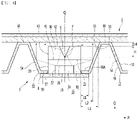
- FIG. 4 is a cross-sectional view of a backlight unit laid down according to an embodiment of the present disclosure.
- a display device may include a display panel 1 to display an image, an optical sheet 2 which faces the display panel 1, and a backlight unit 3 to emit light toward the optical sheet 2.
- the display panel 1 may be an LCD panel or an LED panel, and may be provided in various types as long as displaying an image by light emitted from the backlight unit 3.
- the optical sheet 2 may be formed the form of the combination of a plurality of sheets, and may include, for example, at least one diffusion sheet and at least one prism sheet.
- the backlight unit 3 includes an LED package 20 (hereinafter, referred to as an LED package) serving as a light source.
- the backlight unit 3 may be a top view type backlight unit in which a direction (Q, hereinafter, referred to as an optical axis direction) of light emitted from the LED package 20 is directed toward the display panel 1.
- the optical axis direction "Q" may be in a vertical direction on the basis of when the display device is laid down, and the optical axis direction "Q" may be a front-rear direction on the basis of when the display device is in an upright state.
- the backlight unit 3 includes at least one substrate 8, a plurality of light emitting units 10, and a reflector 50.
- the backlight unit 3 may further include a case 7, and at least one substrate 7 may be mounted in the case 7.
- the substrate 7 may be a PCB.
- the substrate 8 may be mounted in the case 7 to correspond to the light emitting unit 10 in a 1: 1 correspondence, and may be mounted, in number smaller than the number of light emitting units 10, in the case 7.
- a plurality of light emitting units 10 may be mounted on the PCB 8.
- the backlight unit 3 may include a plurality of PCBs 8 on which a plurality of light emitting units 10 are mounted.
- Each of the plurality of light emitting units 10 may be mounted on the substrate 8.
- the reflector 50 includes a reflector unit 52 to receive the light emitting unit 10 therein.
- the reflector unit 52 is formed to be larger than the light emitting unit 10, and the light emitting unit 10 is received in a space "S" defined inside the reflector unit 52, and the reflector unit 52 surrounds the outer circumference of the light emitting unit 10.
- the outer circumference of the light emitting unit 10 may be defined with an outer circumference of the LED package 10 and an outer circumference of a light diffusion layer 40, which are to be described later.
- the light emitting unit 10 and the reflector unit 52 correspond to each other at the ratio of 1:1, and the backlight unit 3 has one light emitting unit 10 received in one reflector unit 52.
- the reflector 50 includes a plurality of reflector units 52 to receive a plurality of light emitting units 10.
- the reflector 50 includes a plurality of reflector units 52 having spaces "S" for receiving a plurality of light emitting units 10, respectively.
- the reflector 50 may have a rectangular shape in an outer edge thereof.
- the plurality of reflector units 52 may be consecutively formed in the front-rear direction and a left-right direction, and the plurality of light emitting units 10 may be spaced apart from each other in the front-rear direction and the left-right direction.
- the plurality of reflector units 52 When the backlight unit 3 is in the upright state in the vertical direction, the plurality of reflector units 52 may be consecutively formed in the vertical direction and the left-right direction, and the plurality of light emitting units 10 may be spaced apart from each other in the vertical direction and the left-right direction.
- Each of the plurality of light emitting units 10 includes an LED package 20 and the light diffusion layer 4C integrally formed with the LED package 20.
- a bottom surface 21 of the LED package 20 is mounted on a top surface of the substrate 8, the top surface of the LED package 20 is an opposite surface 22 to the bottom surface 21 of the LED package 20, and the top surface of the LED package 20 is a surface which faces the light diffusion layer 40.
- the LED package 20 may include an LED chip light source 24 and a phosphor 30.
- the LED chip light source 24 may include a blue LED chip
- the phosphor 30 may be a yellow phosphor covering the blue LED chip.
- the LED chip light source 24 may include a blue LED chip
- the phosphor 30 may include all of a yellow phosphor, a red phosphor, and a green phosphor.
- a bottom surface of the LED chip light source 24 may make contact with the top surface of the substrate 8.
- a top surface 26 and a circumferential surface 27 of the LED chip light source 24 may be covered by the phosphor 30, and the phosphor 30 may surround the top surface 26 and an outer circumference 27 of the LED chip light source 24.
- the phosphor 30 may be in a polygonal shape, for example, in a hexahedron shape.
- the bottom surface of the LED chip light source 24 and the bottom surface of the phosphor 30 may form the bottom surface 21 of the LED package 20.
- the top surface of the phosphor 30 may be the top surface 22 of the LED package 20, and the outer circumference of the phosphor 30 may be the outer circumference 23 of the LED package 20.
- the light diffusion layer 40 which widely diffuses light emitted from the LED package 20 to the surroundings, may be formed of a material and a shape capable of diffusing the light to the surroundings.
- the light diffusion layer 40 is formed on the opposite surface 22 of the substrate 8 of the LED package 20.
- the light diffusion layer 40 may cover the top surface 22 of the LED package 20.
- the light diffusion layer 40 may be formed on a top surface of the phosphor 30.
- the area of the bottom surface 41 of the light diffusion layer 40 may be equal to the area of the top surface of the LED package 20.
- the bottom surface 41 of the light diffusion layer 40 may be integrated with the top surface 22 of the LED package 20, that is, the top surface of the phosphor 30, and the bottom surface 41 of the light diffusion layer 40 and the top surface 22 of the LED package 20 may be substantially the same surface, and this surface may be a boundary between the light diffusion layer 40 and the LED package 20.
- the top surface 42 of the light diffusion layer 40 faces the optical sheet 2, and the outer circumference 43 of the light diffusion layer 40 faces the inner surface 53 of the reflector unit 52.
- the light diffusion layer 40 includes a circumferential surface 43 connecting the bottom surface 41 to the top surface 42.
- the light diffusion layer 40 may be substantially in a hexahedron shape.
- the circumferential surface 43 of the light diffusion layer 40 may include four sides of a left side, a right side, a front side, and a rear side.
- the circumferential surface 43 of the light diffusion layer 40 may face the inner surface 53 of the reflector unit 52 in a direction perpendicular to the optical axis "Q".
- the light diffusion layer 40 may include a TiO 2 coating layer applied to the top surface of the phosphor 30.
- a groove “G” is formed in the top surface 42 of the light diffusion layer 40.
- the shape of the longitudinal-section of the groove “G” may be triangular, and may extend in a stripe shape from one end of the light diffusion layer 40 to an opposite end of the light diffusion layer 40.
- a part, which includes the groove "G", of the light diffusion layer 40 may include a pair of inclined surfaces which faces in a direction "R" perpendicular to the optical axis direction "Q", and bottom surfaces of the pair of inclined surfaces may be connected to each other while forming a V shape.
- the inclined surface may be formed to have an acute angle with respect to an extension line extending in the optical axis direction "Q" from a vertex to which the pair of inclined surfaces are connected.
- each of the pair of inclined surfaces forming the groove "G" and the top surface 42 of the light diffusion layer 40 may be formed to have an obtuse angle.
- the groove “G” may be cross-shaped when viewed from above the light diffusion layer 40 on the basis of when the backlight unit is laid down in the horizontal direction.
- the groove “G” may include a first groove “G1” having a long stripe shape extending in the vertical direction on the basis of when the backlight unit is in the upright state, and a second groove “G2” having a long stripe shape extending in the left-right direction.
- the first groove “G1" may cross the second groove "G2".
- the top surface 42 of the light diffusion layer 40 may be a flat surface instead of a curved surface.
- the groove “G” formed in the top surface 42 of the light diffusion layer 40 is recessed in the flat surface.
- the groove “G” may be recessed at an equal depth “H” (see FIG. 4 ) in the top surface 42 of the light diffusion layer 34 while extending lengthwise of the groove "G".
- the top surface 42 of the light diffusion layer 40 may be defined as a part without the groove "G" when viewed from above the light diffusion layer 40, and the distance "L4" (see FIG. 4 ) between the top surface 42 of the light diffusion layer 40 and the optical sheet 2 may be constant
- a distance "L4" between the top surface 42 of the light diffusion layer 40 and the optical sheet 2 may be the distance in the vertical direction (i.e., the optical axis direction Q), and the top surface 42 of the light diffusion layer 40 may be at the equal distance from the optical sheet 2 regardless of the position.
- the plurality of reflector units 52 constituting the reflector 50 may be integrally formed.
- the reflector 50 may be a foaming reflector in which the plurality of reflector units 52 are integrally foamed.
- Each of the plurality of reflector units 52 includes a wall 54 for defining the space "S".
- the wall 54 for forming the space "S" surrounds the outer circumference 23 of the LED package 20 and the outer circumference 43 of the light diffusion layer 40.
- the space “S” is formed to be more expanded, as the space “S" farther away from the substrate 8.
- the wall 54 may be in a three-dimensional shape.
- the wall 54 may include a left wall, a right wall, a front wall, and a rear wall on the basis of when the backlight unit is laid down in the horizontal direction, and the space "S" surrounded by the left wall, the right wall, the front wall, and the rear wall may be defined as a space for receiving the light emitting unit 10.
- the wall 54 may include a left wall, a right wall, a front wall, and a rear wall on the basis of when the backlight unit is in the upright state in the vertical direction, and the space "S" surrounded by the left wall, the right wall, the front wall, and the rear wall may be defined as a space for receiving the light emitting unit 10.
- An inner surface 53 of the wall 54 may include an inclined surface inclined with respect to the optical axis direction "Q" of the light emitting unit 20.
- the inclined surface may be formed at an acute angle with respect to the optical axis direction "Q".
- an outer surface 55 of the wall 54 may be spaced from an outer surface 55 of a wall 54 of the adjacent another reflector unit 52.
- the inner surface 53 of the wall 54 may be an inclined surface substantially, and the inner surface 53 of the wall 54 and the inclined surface are assigned with the same reference numeral '53'.
- the wall 54 may be inclined with respect to the optical axis direction "Q", like the inclined surface 53. Such a wall 54 may be formed at an acute angle with respect to the optical axis direction "Q".
- Each of the plurality of reflector units 52 may further include a base 56 extending from the wall 54, and one surface 56A of the base 56 which faces the optical sheet 2.
- the base 56 may be formed in a direction "R" perpendicular to the optical axis direction "Q".
- the base 56 may be formed therein with a hole 57 to surround a portion of the outer circumference 23 of the LED package 20. That is, each of the plurality of reflector units 52 may include the wall 54 and the base 56.
- each reflector unit 52 may be directly connected to the wall 54 of the adjacent reflector unit 52, and the wall 54 of each reflector unit 52 may be connected with the wall 54 of the adjacent another reflector unit 52 through an additional connecting body 5
- the plurality of reflector units 52 may be spaced apart from each other through the connecting body 58.
- the plurality of reflector units 52 and the connecting body 58 may be integrally foamed, and the connecting body 58 may be substantially formed in a lattice shape.
- the boundary between the LED package 20 and the light diffusion layer 40 and each top surface 22 of the light diffusion layer 40 may face the inclined surface 53.
- the boundary between the LED package 20 and the light diffusion layer 40 may be the top surface 22 of the LED package 20 and may be the bottom surface 41 of the light diffusion layer 40.
- the boundary between the LED package 20 and the light diffusion layer 40 will be described with reference numeral '41', and will be named a "boundary 41" for the illustrative purpose.
- the bottom surface 21 of the LED package 20, the boundary 41 between the LED package 20 and the light diffusion layer 40, and the top surface 42 of the light diffusion layer 40 may be spaced apart from the wall 44.
- a first distance "L1" between the bottom surface 21 of the LED package 20 and the wall 44 is shorter than a second distance 'L2' between the boundary 41 and the wall 44, and the third distance 'L3' between the top surface 42 of the light diffusion layer 40 and the wall 44 may be longer than the second distance 'L2'.
- Each of the first distance 'L1', the second distance 'L2', and the third distance 'L3' may be a distance in the direction 'R' perpendicular to the optical axis direction 'Q'.
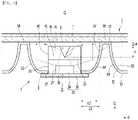
- FIG. 5 is a front view of a backlight unit laid down according to another embodiment of the present disclosure.
- the shape of a wall 53' of the reflector unit 52 may be different from the shape of a wall 53 of the reflector unit 52 as illustrated in FIG. 4 .
- An inner surface 53 ' of the reflector unit 52 may be a curved surface, and a wall 54 ' of the reflector unit 52 may be formed to have the shape of being gently curved at a lower portion thereof and sharply curved toward an upper portion thereof.
- the outer surface 55 ' of the reflector unit 52 may be also be curved.
- such a reflector unit 52 may be in a hemispherical shape.
- the reflector unit 52 may be formed in the center thereof with a hole 57 to surround a portion of an outer circumferential surface of the LED package 20.
- the substrate 8, the LED package 20, the light diffusion layer 40, and the optical sheet 2 are identical to or similar to those of the backlight unit illustrated in FIG. 4 . Accordingly, the following description will be made with the same reference numerals to avoid redundancy.
- Each of the outer circumference 23 of the LED package 20 and the outer circumference 43 of the light diffusion layer 40 may face the inner surface 53', which is formed in the curved shape, of the reflector unit 52 in a direction perpendicular to the optical axis direction "Q".
Landscapes
- Physics & Mathematics (AREA)
- Nonlinear Science (AREA)
- General Physics & Mathematics (AREA)
- Optics & Photonics (AREA)
- Mathematical Physics (AREA)
- Chemical & Material Sciences (AREA)
- Crystallography & Structural Chemistry (AREA)
- Engineering & Computer Science (AREA)
- General Engineering & Computer Science (AREA)
- Microelectronics & Electronic Packaging (AREA)
- Planar Illumination Modules (AREA)
Description
- The present disclosure relates to a backlight unit and a display device having the same.
- As the information society is developed, the demand for a display device is increasing in various forms. In match to the demand, various display devices, such as a liquid crystal display device (LCD), a plasma display panel (PDP), an electro luminescent display (ELD), an organic light emitting diode (OLED), and a vacuum fluorescent display (VFD), have been studied and used.
- Some of the display devices may include a backlight unit to emit light to a display panel.
- The backlight unit is classified into an edge type backlight unit and a direct type backlight unit depending on the position of a light source.
- The edge type backlight unit excellently represents the uniformity of light, because light sources are disposed on left and right side surfaces or left and right side surfaces of the display panel and the light is uniformly dispersed on the front surface of the display panel using a light guide plate.
- Meanwhile, the direct type backlight unit may be mainly used for a large scale display requiring higher brightness, because a plurality of light sources are disposed under the display panel and a light efficiency is more excellently represented as compared to that of the edge type backlight unit.
-
Korean Patent Registration No. 10-1832311 B1 (published on Feb. 26, 2018 -
CN 104 696 780 A1 relates to a direct type backlight module and its light source assembly. -
US 2013/013252 A1 relates to a light-emitting device, a display apparatus, and a method for designing a reflective member. - The invention is defined by the claims.
- According to the backlight unit of the related art, the process and the time to insert the lens into the reflector may be required, and image quality may be degraded when the light source module and the lens are misaligned from each other in optical axis.
- According to the backlight unit of the related art, when the lens has a thicker thickness, the whole thickness of the backlight unit may be increased.
- The present disclosure is to provide a backlight unit capable of simplifying the assembling process, reducing the manufacturing time, and minimizing image quality, and a display device having the same.
- The present disclosure is to provide a backlight unit which can be realized in slim size, and a display device having the same.
- According to an embodiment of the present disclosure, a backlight unit may include a plurality of light emitting units, and a reflector having a reflector unit formed to have a space to receive each of the plurality of light emitting units.
- Each light emitting unit may include an LED package mounted on a substrate, and a light diffusion layer formed on an opposite surface of the substrate in the LED package, formed with a groove in a top surface, and having an outer circumference which faces an inner surface of the reflector unit.
- A plurality of reflector units may be integrally foamed in the reflector.
- The space is expanded as the space is away from the substrate.
- A wall defining the space surrounds an outer circumference of the LED package and an outer circumference of the light diffusion layer.
- The LED package may include an LED chip light source, and a phosphor to surround a top surface and an outer circumference of the LED chip light source.
- The light diffusion layer may be formed on a top surface of the phosphor.
- The light diffusion layer may be a TiO2 coating layer applied to the top surface of the phosphor.
- A shape of a longitudinal-section of the groove may be a triangular shape, and may extend in a stripe shape from one end of the light diffusion layer to an opposite end of the light diffusion layer.
- The groove may have a cross shape when viewed from above the light diffusion layer.
- An inner surface of the wall may include an inclined surface inclined with respect to an optical axis direction of the light emitting unit.
- Each of a boundary between the LED package and the light diffusion layer and a top surface of the light diffusion layer faces the inclined surface.
- Each of a bottom surface of the LED package, a boundary between the LED package and the light diffusion layer, and a top surface of the light diffusion layer may be spaced apart from the wall.
- A first distance between the bottom surface of the LED package and the wall may be shorter than a second distance between the boundary and the wall.
- A third distance between the top surface of the light diffusion layer and the wall may be longer than the second distance.
- According to an embodiment of the present disclosure, a display device having a backlight unit may include a display panel, an optical sheet which faces the display panel, the backlight unit to emit light toward the optical sheet. In addition, the top surface of the light diffusion layer constituting the backlight unit may face the optical sheet. The top surface of the light diffusion layer may be a flat surface, a groove may be formed in the top surface of the light diffusion layer, and the distance between the top surface of the light diffusion layer and the optical sheet may be uniform.
- According to an embodiment of the present disclosure, the light emitting unit includes the light diffusion layer integrally formed with the LED package to diffuse the light to the reflector, and the light diffused around the light diffusion layer is reflected from the reflector, thereby simplifying the assembly process and shortening the manufacturing time as compared to when a separate lens is installed instead of the light diffusion layer.
- In addition, since the light diffusion layer is integrally formed with the LED package, compactness may be realized as compared to when the separate lens is mounted instead of the light diffusion layer, and the slim backlight unit may be realized.
-
-
FIG. 1 is an exploded perspective view of a display device having a backlight unit according to an embodiment of the present disclosure. -
FIG. 2 is a front view of a backlight unit in an upright state according to an embodiment of the present disclosure. -
FIG. 3 is a side view of a reflector in an upright state according to an embodiment of the present disclosure. -
FIG. 4 is a cross-sectional view of a backlight unit laid down according to an embodiment of the present disclosure. -
FIG. 5 is a front view of a backlight unit laid down according to another embodiment of the present disclosure. - Hereinafter, the detailed embodiment of the present disclosure will be described in detail with reference to accompanying drawings.
-
FIG. 1 is an exploded perspective view of a display device having a backlight unit according to an embodiment of the present disclosure.FIG. 2 is a front view of a backlight unit in an upright state according to an embodiment of the present disclosure.FIG. 3 is a side view of a reflector in an upright state according to an embodiment of the present disclosure.FIG. 4 is a cross-sectional view of a backlight unit laid down according to an embodiment of the present disclosure. - A display device may include a display panel 1 to display an image, an
optical sheet 2 which faces the display panel 1, and abacklight unit 3 to emit light toward theoptical sheet 2. - The display panel 1 may be an LCD panel or an LED panel, and may be provided in various types as long as displaying an image by light emitted from the
backlight unit 3. - The
optical sheet 2 may be formed the form of the combination of a plurality of sheets, and may include, for example, at least one diffusion sheet and at least one prism sheet. - The
backlight unit 3 includes an LED package 20 (hereinafter, referred to as an LED package) serving as a light source. In addition, thebacklight unit 3 may be a top view type backlight unit in which a direction (Q, hereinafter, referred to as an optical axis direction) of light emitted from theLED package 20 is directed toward the display panel 1. - According to the present specification, the optical axis direction "Q" may be in a vertical direction on the basis of when the display device is laid down, and the optical axis direction "Q" may be a front-rear direction on the basis of when the display device is in an upright state.
- The
backlight unit 3 includes at least onesubstrate 8, a plurality oflight emitting units 10, and areflector 50. - The
backlight unit 3 may further include acase 7, and at least onesubstrate 7 may be mounted in thecase 7. Thesubstrate 7 may be a PCB. - The
substrate 8 may be mounted in thecase 7 to correspond to thelight emitting unit 10 in a 1: 1 correspondence, and may be mounted, in number smaller than the number oflight emitting units 10, in thecase 7. A plurality oflight emitting units 10 may be mounted on thePCB 8. Thebacklight unit 3 may include a plurality ofPCBs 8 on which a plurality of light emittingunits 10 are mounted. - Each of the plurality of light emitting
units 10 may be mounted on thesubstrate 8. - The
reflector 50 includes areflector unit 52 to receive thelight emitting unit 10 therein. Thereflector unit 52 is formed to be larger than thelight emitting unit 10, and thelight emitting unit 10 is received in a space "S" defined inside thereflector unit 52, and thereflector unit 52 surrounds the outer circumference of thelight emitting unit 10. - In this case, the outer circumference of the
light emitting unit 10 may be defined with an outer circumference of theLED package 10 and an outer circumference of alight diffusion layer 40, which are to be described later. - The
light emitting unit 10 and thereflector unit 52 correspond to each other at the ratio of 1:1, and thebacklight unit 3 has onelight emitting unit 10 received in onereflector unit 52. - The
reflector 50 includes a plurality ofreflector units 52 to receive a plurality of light emittingunits 10. - The
reflector 50 includes a plurality ofreflector units 52 having spaces "S" for receiving a plurality of light emittingunits 10, respectively. - The
reflector 50 may have a rectangular shape in an outer edge thereof. - When the
backlight unit 3 is laid down in the horizontal direction, the plurality ofreflector units 52 may be consecutively formed in the front-rear direction and a left-right direction, and the plurality of light emittingunits 10 may be spaced apart from each other in the front-rear direction and the left-right direction. - When the
backlight unit 3 is in the upright state in the vertical direction, the plurality ofreflector units 52 may be consecutively formed in the vertical direction and the left-right direction, and the plurality of light emittingunits 10 may be spaced apart from each other in the vertical direction and the left-right direction. - Each of the plurality of light emitting
units 10 includes anLED package 20 and the light diffusion layer 4C integrally formed with theLED package 20. - Referring to
FIG. 4 , abottom surface 21 of theLED package 20 is mounted on a top surface of thesubstrate 8, the top surface of theLED package 20 is anopposite surface 22 to thebottom surface 21 of theLED package 20, and the top surface of theLED package 20 is a surface which faces thelight diffusion layer 40. - The
LED package 20 may include an LEDchip light source 24 and aphosphor 30. - For example, in the
LED package 20, the LEDchip light source 24 may include a blue LED chip, and thephosphor 30 may be a yellow phosphor covering the blue LED chip. - For another example, in the
LED package 20, the LEDchip light source 24 may include a blue LED chip, and thephosphor 30 may include all of a yellow phosphor, a red phosphor, and a green phosphor. - A bottom surface of the LED
chip light source 24 may make contact with the top surface of thesubstrate 8. Atop surface 26 and acircumferential surface 27 of the LEDchip light source 24 may be covered by thephosphor 30, and thephosphor 30 may surround thetop surface 26 and anouter circumference 27 of the LEDchip light source 24. - The
phosphor 30 may be in a polygonal shape, for example, in a hexahedron shape. - The bottom surface of the LED
chip light source 24 and the bottom surface of thephosphor 30 may form thebottom surface 21 of theLED package 20. - The top surface of the
phosphor 30 may be thetop surface 22 of theLED package 20, and the outer circumference of thephosphor 30 may be theouter circumference 23 of theLED package 20. - The
light diffusion layer 40, which widely diffuses light emitted from theLED package 20 to the surroundings, may be formed of a material and a shape capable of diffusing the light to the surroundings. - The
light diffusion layer 40 is formed on theopposite surface 22 of thesubstrate 8 of theLED package 20. Thelight diffusion layer 40 may cover thetop surface 22 of theLED package 20. Thelight diffusion layer 40 may be formed on a top surface of thephosphor 30. The area of thebottom surface 41 of thelight diffusion layer 40 may be equal to the area of the top surface of theLED package 20. - The
bottom surface 41 of thelight diffusion layer 40 may be integrated with thetop surface 22 of theLED package 20, that is, the top surface of thephosphor 30, and thebottom surface 41 of thelight diffusion layer 40 and thetop surface 22 of theLED package 20 may be substantially the same surface, and this surface may be a boundary between thelight diffusion layer 40 and theLED package 20. - The
top surface 42 of thelight diffusion layer 40 faces theoptical sheet 2, and theouter circumference 43 of thelight diffusion layer 40 faces theinner surface 53 of thereflector unit 52. - The
light diffusion layer 40 includes acircumferential surface 43 connecting thebottom surface 41 to thetop surface 42. Thelight diffusion layer 40 may be substantially in a hexahedron shape. In the case, thecircumferential surface 43 of thelight diffusion layer 40 may include four sides of a left side, a right side, a front side, and a rear side. Thecircumferential surface 43 of thelight diffusion layer 40 may face theinner surface 53 of thereflector unit 52 in a direction perpendicular to the optical axis "Q". - The
light diffusion layer 40 may include a TiO2 coating layer applied to the top surface of thephosphor 30. - A groove "G" is formed in the
top surface 42 of thelight diffusion layer 40. The shape of the longitudinal-section of the groove "G" may be triangular, and may extend in a stripe shape from one end of thelight diffusion layer 40 to an opposite end of thelight diffusion layer 40. - A part, which includes the groove "G", of the
light diffusion layer 40 may include a pair of inclined surfaces which faces in a direction "R" perpendicular to the optical axis direction "Q", and bottom surfaces of the pair of inclined surfaces may be connected to each other while forming a V shape. The inclined surface may be formed to have an acute angle with respect to an extension line extending in the optical axis direction "Q" from a vertex to which the pair of inclined surfaces are connected. - In addition, each of the pair of inclined surfaces forming the groove "G" and the
top surface 42 of thelight diffusion layer 40 may be formed to have an obtuse angle. - The groove "G" may be cross-shaped when viewed from above the
light diffusion layer 40 on the basis of when the backlight unit is laid down in the horizontal direction. The groove "G" may include a first groove "G1" having a long stripe shape extending in the vertical direction on the basis of when the backlight unit is in the upright state, and a second groove "G2" having a long stripe shape extending in the left-right direction. The first groove "G1" may cross the second groove "G2". - The
top surface 42 of thelight diffusion layer 40 may be a flat surface instead of a curved surface. The groove "G" formed in thetop surface 42 of thelight diffusion layer 40 is recessed in the flat surface. The groove "G" may be recessed at an equal depth "H" (seeFIG. 4 ) in thetop surface 42 of the light diffusion layer 34 while extending lengthwise of the groove "G". - The
top surface 42 of thelight diffusion layer 40 may be defined as a part without the groove "G" when viewed from above thelight diffusion layer 40, and the distance "L4" (seeFIG. 4 ) between thetop surface 42 of thelight diffusion layer 40 and theoptical sheet 2 may be constant - In this case, a distance "L4" between the
top surface 42 of thelight diffusion layer 40 and theoptical sheet 2 may be the distance in the vertical direction (i.e., the optical axis direction Q), and thetop surface 42 of thelight diffusion layer 40 may be at the equal distance from theoptical sheet 2 regardless of the position. - The plurality of
reflector units 52 constituting thereflector 50 may be integrally formed. Thereflector 50 may be a foaming reflector in which the plurality ofreflector units 52 are integrally foamed. - Each of the plurality of
reflector units 52 includes awall 54 for defining the space "S". - The
wall 54 for forming the space "S" surrounds theouter circumference 23 of theLED package 20 and theouter circumference 43 of thelight diffusion layer 40. - The space "S" is formed to be more expanded, as the space "S" farther away from the
substrate 8. Thewall 54 may be in a three-dimensional shape. - The
wall 54 may include a left wall, a right wall, a front wall, and a rear wall on the basis of when the backlight unit is laid down in the horizontal direction, and the space "S" surrounded by the left wall, the right wall, the front wall, and the rear wall may be defined as a space for receiving thelight emitting unit 10. - The
wall 54 may include a left wall, a right wall, a front wall, and a rear wall on the basis of when the backlight unit is in the upright state in the vertical direction, and the space "S" surrounded by the left wall, the right wall, the front wall, and the rear wall may be defined as a space for receiving thelight emitting unit 10. - An
inner surface 53 of thewall 54 may include an inclined surface inclined with respect to the optical axis direction "Q" of thelight emitting unit 20. The inclined surface may be formed at an acute angle with respect to the optical axis direction "Q". - Meanwhile, an
outer surface 55 of thewall 54 may be spaced from anouter surface 55 of awall 54 of the adjacent anotherreflector unit 52. Theinner surface 53 of thewall 54 may be an inclined surface substantially, and theinner surface 53 of thewall 54 and the inclined surface are assigned with the same reference numeral '53'. - The
wall 54 may be inclined with respect to the optical axis direction "Q", like theinclined surface 53. Such awall 54 may be formed at an acute angle with respect to the optical axis direction "Q". - Each of the plurality of
reflector units 52 may further include a base 56 extending from thewall 54, and onesurface 56A of the base 56 which faces theoptical sheet 2. The base 56 may be formed in a direction "R" perpendicular to the optical axis direction "Q". The base 56 may be formed therein with ahole 57 to surround a portion of theouter circumference 23 of theLED package 20. That is, each of the plurality ofreflector units 52 may include thewall 54 and thebase 56. - Meanwhile, in the
reflector 50, thewall 54 of eachreflector unit 52 may be directly connected to thewall 54 of theadjacent reflector unit 52, and thewall 54 of eachreflector unit 52 may be connected with thewall 54 of the adjacent anotherreflector unit 52 through an additional connecting body 5 In this case, the plurality ofreflector units 52 may be spaced apart from each other through the connectingbody 58. - The plurality of
reflector units 52 and the connectingbody 58 may be integrally foamed, and the connectingbody 58 may be substantially formed in a lattice shape. - The boundary between the
LED package 20 and thelight diffusion layer 40 and eachtop surface 22 of thelight diffusion layer 40 may face theinclined surface 53. - The boundary between the
LED package 20 and thelight diffusion layer 40 may be thetop surface 22 of theLED package 20 and may be thebottom surface 41 of thelight diffusion layer 40. Hereinafter, for the convenience of explanation, the boundary between theLED package 20 and thelight diffusion layer 40 will be described with reference numeral '41', and will be named a "boundary 41" for the illustrative purpose. - The
bottom surface 21 of theLED package 20, theboundary 41 between theLED package 20 and thelight diffusion layer 40, and thetop surface 42 of thelight diffusion layer 40 may be spaced apart from the wall 44. - A first distance "L1" between the
bottom surface 21 of theLED package 20 and the wall 44 is shorter than a second distance 'L2' between theboundary 41 and the wall 44, and the third distance 'L3' between thetop surface 42 of thelight diffusion layer 40 and the wall 44 may be longer than the second distance 'L2'. - Each of the first distance 'L1', the second distance 'L2', and the third distance 'L3' may be a distance in the direction 'R' perpendicular to the optical axis direction 'Q'.
-
FIG. 5 is a front view of a backlight unit laid down according to another embodiment of the present disclosure. - According to the present embodiment, the shape of a wall 53' of the
reflector unit 52 may be different from the shape of awall 53 of thereflector unit 52 as illustrated inFIG. 4 . An inner surface 53 ' of thereflector unit 52 may be a curved surface, and a wall 54 ' of thereflector unit 52 may be formed to have the shape of being gently curved at a lower portion thereof and sharply curved toward an upper portion thereof. The outer surface 55 ' of thereflector unit 52 may be also be curved. For example, such areflector unit 52 may be in a hemispherical shape. - The
reflector unit 52 may be formed in the center thereof with ahole 57 to surround a portion of an outer circumferential surface of theLED package 20. - The
substrate 8, theLED package 20, thelight diffusion layer 40, and theoptical sheet 2 are identical to or similar to those of the backlight unit illustrated inFIG. 4 . Accordingly, the following description will be made with the same reference numerals to avoid redundancy. - Each of the
outer circumference 23 of theLED package 20 and theouter circumference 43 of thelight diffusion layer 40 may face the inner surface 53', which is formed in the curved shape, of thereflector unit 52 in a direction perpendicular to the optical axis direction "Q". - Hereinabove, although the present disclosure has been described with reference to exemplary embodiments and the accompanying drawings, the present disclosure is not limited thereto, but may be variously modified and altered by those skilled in the art to which the present disclosure pertains without departing from the scope of the present disclosure claimed in the following claims.
- Therefore, the exemplary embodiments of the present disclosure are provided to explain the present disclosure, but the present disclosure is not limited by the embodiments.
Claims (10)
- A backlight unit (3) comprising:a plurality of light emitting units (10); anda reflector (50) including a plurality of reflector units (52) formed to have spaces (S) for receiving the plurality of light emitting units (10), respectively,wherein each light emitting unit (10) includes:an LED package (20) mounted on a substrate (8), the LED package (20) having a bottom surface (21) facing the substrate (8) and a top surface (22) opposite to the bottom surface (21);wherein each space (S) is formed by a wall (54) which surrounds the outer circumference of a corresponding LED package and is formed in an expanding shape which is larger at an end that is away from the substrate (8); andcharacterized in that each light emitting unit further includes:a light diffusion layer (40) comprising a bottom surface (41), an outer circumferential surface (43) and a top surface (42), the light diffusion layer including a groove (G) formed in its top surface (42), the light diffusion layer (40) being formed on the top surface of the LED package (20) and wherein the outer circumferential surface (43) of the light diffusion layer (40) faces an inner surface (53) of the reflector unit (52),and is surrounded by the corresponding wall (54) of the reflector unit (53).
- The backlight unit of claim 1, wherein the LED package (20) includes:an LED chip light source (24); anda phosphor (30) to surround a top surface (26) and an outer circumference (27) of the LED chip light source (24), andwherein the light diffusion layer (40) is formed on a top surface of the phosphor (30).
- The backlight unit of claim 2, wherein the light diffusion layer (40) is a TiO2 coating layer applied to the top surface of the phosphor (30).
- The backlight unit of claim 1, wherein a shape of a longitudinal-section of the groove (G) is a triangular shape, and extends in a stripe shape from one end of the light diffusion layer (40) to an opposite end of the light diffusion layer (40) .
- The backlight unit of claim 1, wherein the groove (G) has a cross shape when viewed from above the light diffusion layer (40) .
- The backlight unit of claim 1, wherein an inner surface of the wall (44) includes an inclined surface (53) inclined with respect to an optical axis direction of the light emitting unit (10).
- The backlight unit of claim 1, wherein each of a bottom surface of the LED package (20), a boundary (41) between the LED package (20) and the light diffusion layer (40), and a top surface (42) of the light diffusion layer (40) is spaced apart from the wall (44),wherein a first distance (L1) between the bottom surface (21) of the LED package (20) and the wall (44) is shorter than a second distance (L2) between the boundary (41) and the wall (44), andwherein a third distance (L3) between the top surface (42) of the light diffusion layer (40) and the wall (44) is longer than the second distance (L2).
- A display device having a backlight unit (3) according to any one of claims 1 to 7, the display device comprising:a display panel (1);an optical sheet (2) configured to face the display panel (1); andwherein the top surface (42) of the light diffusion layer (40) is a flat surface,except at the location where the groove (G) is formed in the top surface (42) of the light diffusion layer (40), andwherein a distance between the top surface (42) of the light diffusion layer (40) not comprising the groove (G) and the optical sheet (2) is uniform.
- The display device of claim 8, wherein the LED package (20) includes:an LED chip light source (24); anda phosphor (30) to surround a top surface (26) and an outer circumference (27) of the LED chip light source (24), andwherein the light diffusion layer (40) is formed on a top surface of the phosphor (30).
- The display device of claim 8, wherein the light diffusion layer (40) is a TiO2 coating layer applied to the top surface of the phosphor (30).
Applications Claiming Priority (1)
| Application Number | Priority Date | Filing Date | Title |
|---|---|---|---|
| PCT/KR2019/001337 WO2020158976A1 (en) | 2019-01-31 | 2019-01-31 | Backlight unit and display device comprising same |
Publications (3)
| Publication Number | Publication Date |
|---|---|
| EP3760919A1 EP3760919A1 (en) | 2021-01-06 |
| EP3760919A4 EP3760919A4 (en) | 2022-01-19 |
| EP3760919B1 true EP3760919B1 (en) | 2023-01-11 |
Family
ID=71842230
Family Applications (1)
| Application Number | Title | Priority Date | Filing Date |
|---|---|---|---|
| EP19913093.1A Active EP3760919B1 (en) | 2019-01-31 | 2019-01-31 | Backlight unit and display device comprising same |
Country Status (4)
| Country | Link |
|---|---|
| US (1) | US11557578B2 (en) |
| EP (1) | EP3760919B1 (en) |
| KR (1) | KR102477178B1 (en) |
| WO (1) | WO2020158976A1 (en) |
Families Citing this family (12)
| Publication number | Priority date | Publication date | Assignee | Title |
|---|---|---|---|---|
| WO2021035496A1 (en) * | 2019-08-26 | 2021-03-04 | 京东方科技集团股份有限公司 | Backlight module and display apparatus |
| KR102711189B1 (en) * | 2019-11-15 | 2024-09-30 | 엘지디스플레이 주식회사 | Back light unit and display device using the same |
| JP7295437B2 (en) * | 2019-11-29 | 2023-06-21 | 日亜化学工業株式会社 | light emitting device |
| KR102696037B1 (en) * | 2020-01-22 | 2024-08-19 | 삼성디스플레이 주식회사 | Backlight unit and Display device having the same |
| CN112526786B (en) * | 2020-11-27 | 2022-09-27 | 北海惠科光电技术有限公司 | Color film substrate, display panel and display device |
| JP7580029B2 (en) * | 2021-02-25 | 2024-11-11 | 日亜化学工業株式会社 | Light-emitting device and surface light source |
| EP4418040A4 (en) * | 2021-10-13 | 2025-08-20 | Lg Electronics Inc | Display device |
| CN114153095A (en) | 2021-12-02 | 2022-03-08 | 上海中航光电子有限公司 | Backlight module, preparation method thereof and display device |
| CN114236905A (en) * | 2021-12-14 | 2022-03-25 | 武汉华星光电技术有限公司 | Backlight module and liquid crystal display device |
| CN114253029B (en) * | 2021-12-21 | 2023-12-12 | 天马微电子股份有限公司 | Backlight module and display device |
| US12510781B2 (en) * | 2022-03-31 | 2025-12-30 | Hefei Boe Optoelectronics Technology Co., Ltd. | Backlight module and display device |
| JP7866179B2 (en) * | 2022-03-31 | 2026-05-27 | 日亜化学工業株式会社 | Planar light source, liquid crystal display device |
Family Cites Families (12)
| Publication number | Priority date | Publication date | Assignee | Title |
|---|---|---|---|---|
| US6871982B2 (en) * | 2003-01-24 | 2005-03-29 | Digital Optics International Corporation | High-density illumination system |
| JP2004319340A (en) | 2003-04-17 | 2004-11-11 | Kawaguchiko Seimitsu Co Ltd | Backlight unit |
| JP4600257B2 (en) | 2005-11-25 | 2010-12-15 | ソニー株式会社 | Light guide plate, backlight device, manufacturing method thereof, and liquid crystal display device |
| WO2010053193A1 (en) * | 2008-11-10 | 2010-05-14 | シャープ株式会社 | Light-emitting device, surface light source, and display device |
| KR101832311B1 (en) | 2011-06-24 | 2018-02-26 | 엘지이노텍 주식회사 | Display apparatus |
| JP5386551B2 (en) * | 2011-07-06 | 2014-01-15 | シャープ株式会社 | Light emitting device, display device, and reflecting member design method |
| EP3591463B1 (en) | 2011-09-09 | 2022-11-02 | Lg Innotek Co., Ltd. | Lighting unit |
| EP2958096B1 (en) * | 2013-02-14 | 2020-08-26 | LG Electronics Inc. | Display device |
| CN103148449B (en) * | 2013-03-25 | 2015-03-18 | 苏州奥浦迪克光电技术有限公司 | LED (light emitting diode) lens with direct-lit type liquid crystal backlight |
| CN104696780B (en) | 2013-12-05 | 2017-04-26 | 富泰华精密电子(郑州)有限公司 | Backlight module and light source assembly thereof |
| KR102203950B1 (en) * | 2014-02-05 | 2021-01-19 | 삼성디스플레이 주식회사 | Light source module, backlight assembly including the same, and display device including the light source module |
| WO2020067495A1 (en) * | 2018-09-28 | 2020-04-02 | 日亜化学工業株式会社 | Light emitting module and method for producing same |
-
2019
- 2019-01-31 US US17/044,307 patent/US11557578B2/en active Active
- 2019-01-31 EP EP19913093.1A patent/EP3760919B1/en active Active
- 2019-01-31 KR KR1020207026547A patent/KR102477178B1/en active Active
- 2019-01-31 WO PCT/KR2019/001337 patent/WO2020158976A1/en not_active Ceased
Also Published As
| Publication number | Publication date |
|---|---|
| US11557578B2 (en) | 2023-01-17 |
| KR20200111269A (en) | 2020-09-28 |
| EP3760919A4 (en) | 2022-01-19 |
| KR102477178B1 (en) | 2022-12-13 |
| US20210074693A1 (en) | 2021-03-11 |
| EP3760919A1 (en) | 2021-01-06 |
| WO2020158976A1 (en) | 2020-08-06 |
Similar Documents
| Publication | Publication Date | Title |
|---|---|---|
| US11557578B2 (en) | Backlight unit and display device comprising same | |
| US7837360B2 (en) | Optical module | |
| EP1684111B1 (en) | Surface light emitting apparatus | |
| JP6776140B2 (en) | Lighting device | |
| US8480251B2 (en) | Backlight assembly having LEDs and side reflectors and display apparatus having the same | |
| KR101098338B1 (en) | Optic package, optic lens and backlight assembly and display device having the optic package | |
| JP4661735B2 (en) | Surface light source device | |
| JP6685745B2 (en) | Display device | |
| JP5066572B2 (en) | Backlight unit and liquid crystal display device including the same | |
| JP2019091036A (en) | Deformed liquid crystal light emitting device | |
| KR102473400B1 (en) | Back light unit and display device comprising it | |
| US10534219B2 (en) | Array of point light sources contained within segmented reflective partitions | |
| JP2013218940A (en) | Light-emitting module, lighting device including the same, and display device | |
| JP4635863B2 (en) | Surface emitting device | |
| JP2006156231A (en) | Backlight | |
| US9052542B2 (en) | Light source package and backlight unit including the light source package | |
| KR100986541B1 (en) | Light unit and display device having same | |
| CN104712965A (en) | Backlight assembly and display divece having the same | |
| JP5030204B2 (en) | Light emitting diode light source, backlight and liquid crystal display | |
| KR20160078038A (en) | Display apparatus | |
| KR100785448B1 (en) | Light guide plate having a bottom surface with convex surfaces and a backlight panel adopting the same | |
| KR200351685Y1 (en) | backlight panel for color control display | |
| KR20140061006A (en) | Backlight unit and display device having the same | |
| KR20070108501A (en) | Light guide plate having a bottom surface with convex surfaces and a backlight panel adopting the same | |
| KR20190031364A (en) | Light guide plate and backlight unit having the same |
Legal Events
| Date | Code | Title | Description |
|---|---|---|---|
| STAA | Information on the status of an ep patent application or granted ep patent |
Free format text: STATUS: THE INTERNATIONAL PUBLICATION HAS BEEN MADE |
|
| PUAI | Public reference made under article 153(3) epc to a published international application that has entered the european phase |
Free format text: ORIGINAL CODE: 0009012 |
|
| STAA | Information on the status of an ep patent application or granted ep patent |
Free format text: STATUS: REQUEST FOR EXAMINATION WAS MADE |
|
| 17P | Request for examination filed |
Effective date: 20200929 |
|
| AK | Designated contracting states |
Kind code of ref document: A1 Designated state(s): AL AT BE BG CH CY CZ DE DK EE ES FI FR GB GR HR HU IE IS IT LI LT LU LV MC MK MT NL NO PL PT RO RS SE SI SK SM TR |
|
| AX | Request for extension of the european patent |
Extension state: BA ME |
|
| REG | Reference to a national code |
Ref country code: DE Ref legal event code: R079 Ref document number: 602019024432 Country of ref document: DE Free format text: PREVIOUS MAIN CLASS: F21V0008000000 Ipc: G02F0001133570 |
|
| A4 | Supplementary search report drawn up and despatched |
Effective date: 20211217 |
|
| RIC1 | Information provided on ipc code assigned before grant |
Ipc: F21V 8/00 20060101ALI20211213BHEP Ipc: G02F 1/13357 20060101AFI20211213BHEP |
|
| DAV | Request for validation of the european patent (deleted) | ||
| DAX | Request for extension of the european patent (deleted) | ||
| GRAP | Despatch of communication of intention to grant a patent |
Free format text: ORIGINAL CODE: EPIDOSNIGR1 |
|
| STAA | Information on the status of an ep patent application or granted ep patent |
Free format text: STATUS: GRANT OF PATENT IS INTENDED |
|
| INTG | Intention to grant announced |
Effective date: 20220831 |
|
| GRAS | Grant fee paid |
Free format text: ORIGINAL CODE: EPIDOSNIGR3 |
|
| GRAA | (expected) grant |
Free format text: ORIGINAL CODE: 0009210 |
|
| STAA | Information on the status of an ep patent application or granted ep patent |
Free format text: STATUS: THE PATENT HAS BEEN GRANTED |
|
| AK | Designated contracting states |
Kind code of ref document: B1 Designated state(s): AL AT BE BG CH CY CZ DE DK EE ES FI FR GB GR HR HU IE IS IT LI LT LU LV MC MK MT NL NO PL PT RO RS SE SI SK SM TR |
|
| REG | Reference to a national code |
Ref country code: GB Ref legal event code: FG4D |
|
| REG | Reference to a national code |
Ref country code: CH Ref legal event code: EP |
|
| REG | Reference to a national code |
Ref country code: DE Ref legal event code: R096 Ref document number: 602019024432 Country of ref document: DE |
|
| REG | Reference to a national code |
Ref country code: IE Ref legal event code: FG4D |
|
| REG | Reference to a national code |
Ref country code: AT Ref legal event code: REF Ref document number: 1543774 Country of ref document: AT Kind code of ref document: T Effective date: 20230215 |
|
| REG | Reference to a national code |
Ref country code: LT Ref legal event code: MG9D |
|
| REG | Reference to a national code |
Ref country code: NL Ref legal event code: MP Effective date: 20230111 |
|
| REG | Reference to a national code |
Ref country code: AT Ref legal event code: MK05 Ref document number: 1543774 Country of ref document: AT Kind code of ref document: T Effective date: 20230111 |
|
| PG25 | Lapsed in a contracting state [announced via postgrant information from national office to epo] |
Ref country code: NL Free format text: LAPSE BECAUSE OF FAILURE TO SUBMIT A TRANSLATION OF THE DESCRIPTION OR TO PAY THE FEE WITHIN THE PRESCRIBED TIME-LIMIT Effective date: 20230111 |
|
| PG25 | Lapsed in a contracting state [announced via postgrant information from national office to epo] |
Ref country code: RS Free format text: LAPSE BECAUSE OF FAILURE TO SUBMIT A TRANSLATION OF THE DESCRIPTION OR TO PAY THE FEE WITHIN THE PRESCRIBED TIME-LIMIT Effective date: 20230111 Ref country code: PT Free format text: LAPSE BECAUSE OF FAILURE TO SUBMIT A TRANSLATION OF THE DESCRIPTION OR TO PAY THE FEE WITHIN THE PRESCRIBED TIME-LIMIT Effective date: 20230511 Ref country code: NO Free format text: LAPSE BECAUSE OF FAILURE TO SUBMIT A TRANSLATION OF THE DESCRIPTION OR TO PAY THE FEE WITHIN THE PRESCRIBED TIME-LIMIT Effective date: 20230411 Ref country code: LV Free format text: LAPSE BECAUSE OF FAILURE TO SUBMIT A TRANSLATION OF THE DESCRIPTION OR TO PAY THE FEE WITHIN THE PRESCRIBED TIME-LIMIT Effective date: 20230111 Ref country code: LT Free format text: LAPSE BECAUSE OF FAILURE TO SUBMIT A TRANSLATION OF THE DESCRIPTION OR TO PAY THE FEE WITHIN THE PRESCRIBED TIME-LIMIT Effective date: 20230111 Ref country code: HR Free format text: LAPSE BECAUSE OF FAILURE TO SUBMIT A TRANSLATION OF THE DESCRIPTION OR TO PAY THE FEE WITHIN THE PRESCRIBED TIME-LIMIT Effective date: 20230111 Ref country code: ES Free format text: LAPSE BECAUSE OF FAILURE TO SUBMIT A TRANSLATION OF THE DESCRIPTION OR TO PAY THE FEE WITHIN THE PRESCRIBED TIME-LIMIT Effective date: 20230111 Ref country code: AT Free format text: LAPSE BECAUSE OF FAILURE TO SUBMIT A TRANSLATION OF THE DESCRIPTION OR TO PAY THE FEE WITHIN THE PRESCRIBED TIME-LIMIT Effective date: 20230111 |
|
| PG25 | Lapsed in a contracting state [announced via postgrant information from national office to epo] |
Ref country code: SE Free format text: LAPSE BECAUSE OF FAILURE TO SUBMIT A TRANSLATION OF THE DESCRIPTION OR TO PAY THE FEE WITHIN THE PRESCRIBED TIME-LIMIT Effective date: 20230111 Ref country code: PL Free format text: LAPSE BECAUSE OF FAILURE TO SUBMIT A TRANSLATION OF THE DESCRIPTION OR TO PAY THE FEE WITHIN THE PRESCRIBED TIME-LIMIT Effective date: 20230111 Ref country code: IS Free format text: LAPSE BECAUSE OF FAILURE TO SUBMIT A TRANSLATION OF THE DESCRIPTION OR TO PAY THE FEE WITHIN THE PRESCRIBED TIME-LIMIT Effective date: 20230511 Ref country code: GR Free format text: LAPSE BECAUSE OF FAILURE TO SUBMIT A TRANSLATION OF THE DESCRIPTION OR TO PAY THE FEE WITHIN THE PRESCRIBED TIME-LIMIT Effective date: 20230412 Ref country code: FI Free format text: LAPSE BECAUSE OF FAILURE TO SUBMIT A TRANSLATION OF THE DESCRIPTION OR TO PAY THE FEE WITHIN THE PRESCRIBED TIME-LIMIT Effective date: 20230111 |
|
| REG | Reference to a national code |
Ref country code: CH Ref legal event code: PL |
|
| PG25 | Lapsed in a contracting state [announced via postgrant information from national office to epo] |
Ref country code: LU Free format text: LAPSE BECAUSE OF NON-PAYMENT OF DUE FEES Effective date: 20230131 |
|
| REG | Reference to a national code |
Ref country code: BE Ref legal event code: MM Effective date: 20230131 |
|
| REG | Reference to a national code |
Ref country code: DE Ref legal event code: R097 Ref document number: 602019024432 Country of ref document: DE |
|
| PG25 | Lapsed in a contracting state [announced via postgrant information from national office to epo] |
Ref country code: SM Free format text: LAPSE BECAUSE OF FAILURE TO SUBMIT A TRANSLATION OF THE DESCRIPTION OR TO PAY THE FEE WITHIN THE PRESCRIBED TIME-LIMIT Effective date: 20230111 Ref country code: RO Free format text: LAPSE BECAUSE OF FAILURE TO SUBMIT A TRANSLATION OF THE DESCRIPTION OR TO PAY THE FEE WITHIN THE PRESCRIBED TIME-LIMIT Effective date: 20230111 Ref country code: MC Free format text: LAPSE BECAUSE OF FAILURE TO SUBMIT A TRANSLATION OF THE DESCRIPTION OR TO PAY THE FEE WITHIN THE PRESCRIBED TIME-LIMIT Effective date: 20230111 Ref country code: LI Free format text: LAPSE BECAUSE OF NON-PAYMENT OF DUE FEES Effective date: 20230131 Ref country code: EE Free format text: LAPSE BECAUSE OF FAILURE TO SUBMIT A TRANSLATION OF THE DESCRIPTION OR TO PAY THE FEE WITHIN THE PRESCRIBED TIME-LIMIT Effective date: 20230111 Ref country code: DK Free format text: LAPSE BECAUSE OF FAILURE TO SUBMIT A TRANSLATION OF THE DESCRIPTION OR TO PAY THE FEE WITHIN THE PRESCRIBED TIME-LIMIT Effective date: 20230111 Ref country code: CZ Free format text: LAPSE BECAUSE OF FAILURE TO SUBMIT A TRANSLATION OF THE DESCRIPTION OR TO PAY THE FEE WITHIN THE PRESCRIBED TIME-LIMIT Effective date: 20230111 Ref country code: CH Free format text: LAPSE BECAUSE OF NON-PAYMENT OF DUE FEES Effective date: 20230131 |
|
| PLBE | No opposition filed within time limit |
Free format text: ORIGINAL CODE: 0009261 |
|
| STAA | Information on the status of an ep patent application or granted ep patent |
Free format text: STATUS: NO OPPOSITION FILED WITHIN TIME LIMIT |
|
| PG25 | Lapsed in a contracting state [announced via postgrant information from national office to epo] |
Ref country code: SK Free format text: LAPSE BECAUSE OF FAILURE TO SUBMIT A TRANSLATION OF THE DESCRIPTION OR TO PAY THE FEE WITHIN THE PRESCRIBED TIME-LIMIT Effective date: 20230111 Ref country code: BE Free format text: LAPSE BECAUSE OF NON-PAYMENT OF DUE FEES Effective date: 20230131 |
|
| 26N | No opposition filed |
Effective date: 20231012 |
|
| PG25 | Lapsed in a contracting state [announced via postgrant information from national office to epo] |
Ref country code: SI Free format text: LAPSE BECAUSE OF FAILURE TO SUBMIT A TRANSLATION OF THE DESCRIPTION OR TO PAY THE FEE WITHIN THE PRESCRIBED TIME-LIMIT Effective date: 20230111 Ref country code: IE Free format text: LAPSE BECAUSE OF NON-PAYMENT OF DUE FEES Effective date: 20230131 |
|
| PG25 | Lapsed in a contracting state [announced via postgrant information from national office to epo] |
Ref country code: IT Free format text: LAPSE BECAUSE OF FAILURE TO SUBMIT A TRANSLATION OF THE DESCRIPTION OR TO PAY THE FEE WITHIN THE PRESCRIBED TIME-LIMIT Effective date: 20230111 |
|
| PG25 | Lapsed in a contracting state [announced via postgrant information from national office to epo] |
Ref country code: BG Free format text: LAPSE BECAUSE OF FAILURE TO SUBMIT A TRANSLATION OF THE DESCRIPTION OR TO PAY THE FEE WITHIN THE PRESCRIBED TIME-LIMIT Effective date: 20230111 |
|
| PG25 | Lapsed in a contracting state [announced via postgrant information from national office to epo] |
Ref country code: BG Free format text: LAPSE BECAUSE OF FAILURE TO SUBMIT A TRANSLATION OF THE DESCRIPTION OR TO PAY THE FEE WITHIN THE PRESCRIBED TIME-LIMIT Effective date: 20230111 |
|
| PG25 | Lapsed in a contracting state [announced via postgrant information from national office to epo] |
Ref country code: CY Free format text: LAPSE BECAUSE OF FAILURE TO SUBMIT A TRANSLATION OF THE DESCRIPTION OR TO PAY THE FEE WITHIN THE PRESCRIBED TIME-LIMIT; INVALID AB INITIO Effective date: 20190131 |
|
| PG25 | Lapsed in a contracting state [announced via postgrant information from national office to epo] |
Ref country code: HU Free format text: LAPSE BECAUSE OF FAILURE TO SUBMIT A TRANSLATION OF THE DESCRIPTION OR TO PAY THE FEE WITHIN THE PRESCRIBED TIME-LIMIT; INVALID AB INITIO Effective date: 20190131 |
|
| PG25 | Lapsed in a contracting state [announced via postgrant information from national office to epo] |
Ref country code: TR Free format text: LAPSE BECAUSE OF FAILURE TO SUBMIT A TRANSLATION OF THE DESCRIPTION OR TO PAY THE FEE WITHIN THE PRESCRIBED TIME-LIMIT Effective date: 20230111 |
|
| PGFP | Annual fee paid to national office [announced via postgrant information from national office to epo] |
Ref country code: GB Payment date: 20251208 Year of fee payment: 8 |
|
| PGFP | Annual fee paid to national office [announced via postgrant information from national office to epo] |
Ref country code: FR Payment date: 20251209 Year of fee payment: 8 |
|
| PGFP | Annual fee paid to national office [announced via postgrant information from national office to epo] |
Ref country code: DE Payment date: 20251208 Year of fee payment: 8 |