EP3759819B1 - Electronic power switch drive module - Google Patents
Electronic power switch drive module Download PDFInfo
- Publication number
- EP3759819B1 EP3759819B1 EP19706682.2A EP19706682A EP3759819B1 EP 3759819 B1 EP3759819 B1 EP 3759819B1 EP 19706682 A EP19706682 A EP 19706682A EP 3759819 B1 EP3759819 B1 EP 3759819B1
- Authority
- EP
- European Patent Office
- Prior art keywords
- circuit
- power switch
- power semiconductor
- electronic power
- switch drive
- Prior art date
- Legal status (The legal status is an assumption and is not a legal conclusion. Google has not performed a legal analysis and makes no representation as to the accuracy of the status listed.)
- Active
Links
Images



Classifications
-
- H—ELECTRICITY
- H03—ELECTRONIC CIRCUITRY
- H03K—PULSE TECHNIQUE
- H03K17/00—Electronic switching or gating, i.e. not by contact-making and –breaking
- H03K17/08—Modifications for protecting switching circuit against overcurrent or overvoltage
- H03K17/082—Modifications for protecting switching circuit against overcurrent or overvoltage by feedback from the output to the control circuit
- H03K17/0828—Modifications for protecting switching circuit against overcurrent or overvoltage by feedback from the output to the control circuit in composite switches
-
- G—PHYSICS
- G01—MEASURING; TESTING
- G01R—MEASURING ELECTRIC VARIABLES; MEASURING MAGNETIC VARIABLES
- G01R15/00—Details of measuring arrangements of the types provided for in groups G01R17/00 - G01R29/00, G01R33/00 - G01R33/26 or G01R35/00
- G01R15/14—Adaptations providing voltage or current isolation, e.g. for high-voltage or high-current networks
- G01R15/18—Adaptations providing voltage or current isolation, e.g. for high-voltage or high-current networks using inductive devices, e.g. transformers
- G01R15/181—Adaptations providing voltage or current isolation, e.g. for high-voltage or high-current networks using inductive devices, e.g. transformers using coils without a magnetic core, e.g. Rogowski coils
-
- G—PHYSICS
- G01—MEASURING; TESTING
- G01R—MEASURING ELECTRIC VARIABLES; MEASURING MAGNETIC VARIABLES
- G01R15/00—Details of measuring arrangements of the types provided for in groups G01R17/00 - G01R29/00, G01R33/00 - G01R33/26 or G01R35/00
- G01R15/14—Adaptations providing voltage or current isolation, e.g. for high-voltage or high-current networks
- G01R15/20—Adaptations providing voltage or current isolation, e.g. for high-voltage or high-current networks using galvano-magnetic devices, e.g. Hall-effect devices, i.e. measuring a magnetic field via the interaction between a current and a magnetic field, e.g. magneto resistive or Hall effect devices
- G01R15/202—Adaptations providing voltage or current isolation, e.g. for high-voltage or high-current networks using galvano-magnetic devices, e.g. Hall-effect devices, i.e. measuring a magnetic field via the interaction between a current and a magnetic field, e.g. magneto resistive or Hall effect devices using Hall-effect devices
-
- G—PHYSICS
- G01—MEASURING; TESTING
- G01R—MEASURING ELECTRIC VARIABLES; MEASURING MAGNETIC VARIABLES
- G01R15/00—Details of measuring arrangements of the types provided for in groups G01R17/00 - G01R29/00, G01R33/00 - G01R33/26 or G01R35/00
- G01R15/14—Adaptations providing voltage or current isolation, e.g. for high-voltage or high-current networks
- G01R15/20—Adaptations providing voltage or current isolation, e.g. for high-voltage or high-current networks using galvano-magnetic devices, e.g. Hall-effect devices, i.e. measuring a magnetic field via the interaction between a current and a magnetic field, e.g. magneto resistive or Hall effect devices
- G01R15/207—Constructional details independent of the type of device used
-
- H—ELECTRICITY
- H03—ELECTRONIC CIRCUITRY
- H03K—PULSE TECHNIQUE
- H03K17/00—Electronic switching or gating, i.e. not by contact-making and –breaking
- H03K17/51—Electronic switching or gating, i.e. not by contact-making and –breaking characterised by the components used
- H03K17/90—Electronic switching or gating, i.e. not by contact-making and –breaking characterised by the components used by the use, as active elements, of galvano-magnetic devices, e.g. Hall-effect devices
-
- H—ELECTRICITY
- H02—GENERATION; CONVERSION OR DISTRIBUTION OF ELECTRIC POWER
- H02M—APPARATUS FOR CONVERSION BETWEEN AC AND AC, BETWEEN AC AND DC, OR BETWEEN DC AND DC, AND FOR USE WITH MAINS OR SIMILAR POWER SUPPLY SYSTEMS; CONVERSION OF DC OR AC INPUT POWER INTO SURGE OUTPUT POWER; CONTROL OR REGULATION THEREOF
- H02M1/00—Details of apparatus for conversion
- H02M1/0003—Details of control, feedback or regulation circuits
- H02M1/0009—Devices or circuits for detecting current in a converter
-
- H—ELECTRICITY
- H03—ELECTRONIC CIRCUITRY
- H03K—PULSE TECHNIQUE
- H03K2217/00—Indexing scheme related to electronic switching or gating, i.e. not by contact-making or -breaking covered by H03K17/00
- H03K2217/0027—Measuring means of, e.g. currents through or voltages across the switch
Definitions
- the present invention relates to a power semiconductor unit and an electronic power switch drive module therefor.
- electronics switches are used to make and to break electrical connections in circuit arrangements such as half bridges, anti-parallel or series connected switches or simply to connect a load to a power source, for instance applying periodical switching with frequency ranges from hundreds of Hertz to millions of Hertz.
- Electronic switches for power semiconductor units include IGBTs (insulated gate bipolar transistor), FETs (Field Effect Transistor), MOSFETs (Metal Oxide Semiconductor Field Effect Transistor), and various known semiconductor switches that can be arranged in topologies such as a half bridge, three level, matrix and other such semiconductors switch configurations.
- gate drive circuits which may include additional functions such as electrical insulation and bi-directional communication through an insulation barrier:
- Such circuits are typically known as gate drive units (GDU) for semiconductor components such as MOSFETs and IGBTs, whereby the gate drive supplies pulse shaped current waveforms in order to obtain switching times in a range of tenths of microseconds down to nanoseconds for state of the art technology using semiconductors such as SiC or GaN.
- Gate drive units may also perform other functions such as protection against overcurrent. This function can be obtained by measuring the voltage across the semiconductors which increases with higher currents.
- a fast current measuring transducer is advantageous because it is typically more stable over time and over typical operating temperature ranges, and allows switching devices to be operated closer to their known limits.
- an isolated current transducer mounted downstream of the power semiconductor unit and measuring the current flowing in an output conductor of the device may be installed.
- the current transducer is isolated from the power semiconductor unit and may be connected to a control unit of the power semiconductor unit.
- the provision of an isolated current transducer mounted downstream of the power semiconductor unit increases manufacturing and installation costs.
- a measuring shunt resistor however causes energy dissipation and possible thermoelectric offset depending on the range of output voltages. Resistive shunts may also have poor frequency response due to parasitic mutual inductances.
- Japanese Patent document JP2017158407A discloses a motor driver where the the current sensors are Rogowski coils allowing for better detection of faster transients.
- an electronic power switch drive control module for a power semiconductor unit, comprising an electronic power switch drive and a current transducer mounted on one or more circuit boards.
- the electronic power switch drive comprises at least one circuit portion for controlling at least one electronic power switch of a power semiconductor module of said power semiconductor unit.
- the current transducer is configured to be coupled to an output of the power semiconductor module for measuring an output current of the power semiconductor module, said at least one circuit portion connected to an output potential (Vout) of the output current to be measured.
- the current transducer comprises at least one magnetic field sensor, the current transducer being connected to said at least one circuit portion of the electronic power switch drive at said output potential in a non-isolated manner, said at least one circuit portion comprising a control logic circuit (20f) configured for connection to a control board (9) of said power semiconductor module (3), a measurement output signal of the the current transducer being fed into the control logic circuit.
- the current transducer comprises at least one magnetic field sensor, the current transducer being connected to said at least one circuit portion of the electronic power switch drive at said output potential in a non-isolated manner
- the electronic power switch drive module comprises a circuit board on which both the gate drive circuit and current transducer are mounted and interconnected, said circuit board configured to be mounted directly on the power semiconductor module between input terminals and output terminals of the semiconductor module.
- the current transducer comprises a plurality of discrete magnetic field sensors mounted on a portion of a circuit board surrounding a passage formed in the circuit board configured for receiving therethrough the output conductor, the current transducer being connected to said at least one circuit portion of the electronic power switch drive at said output potential in a non-isolated manner.
- the current transducer comprises a passage formed in a current transducer portion of said one or more circuit boards, the passage configured for extension of an output conductor of the power semiconductor module therethrough.
- a Rogowski coil is formed on said current transducer portion of the one or more circuit boards surrounding said passage.
- the current transducer comprises at least one discrete magnetic field sensor mounted on a current transducer portion of the one or more circuit boards.
- the current transducer comprises a plurality of discrete magnetic field sensors mounted on a portion of the circuit board surrounding a passage formed in the portion circuit board configured for receiving therethrough the output conductor.
- At least one of the said discrete magnetic fields sensors is a magnetic field gradient sensor.
- the discrete magnetic field sensor may be a Hall effect sensor.
- the current transducer comprises a signal processing circuit connected to the Rogowski coil magnetic field sensor and to the discrete magnetic field sensors, the signal processing circuit combining the signal of the Rogowski magnetic field sensor and the discrete magnetic field sensors for generating a measurement signal of the output current.
- the electronic power switch drive module comprises a single circuit board on which both the gate drive circuit and current transducer are mounted.
- the electronic power switch drive module may comprise connection studs for connecting the electronic power switch drive module to the power semiconductor module .
- the electronic power switch drive module may comprise a signal or data communication interface for connection to a control unit of the power semiconductor unit.
- At least one circuit portion comprises a local protection circuit connected to an output of the current transducer, the local protection circuit connected to drive circuits of transistors of the power semiconductor module.
- the gate drive circuit comprises an isolated connection to an interface circuit for data, power or both data and power connection to the power semiconductor module.
- a power semiconductor unit comprising an electronic power switch drive module as set forth above, and a power semiconductor module, the electronic power switch drive module being mounted on the power semiconductor module.
- the power semiconductor unit may comprise direct current input terminals on one end of the power semiconductor unit and output terminals arranged on an opposite end of the power semiconductor unit, the electronic power switch drive module being mounted on the power semiconductor module between the input terminals and output terminals.
- the power semiconductor unit is an IGBT device.
- a power semiconductor unit 1 comprises a power semiconductor module 3 and an electronic power switch drive module 2 mounted and connected to the power semiconductor module.
- the power semiconductor module 3 may for instance be in the form of an insulated gate bipolar transistor (IGBT) half bridge module, comprising a power input 5 and a power output 7.
- the power input 5 may comprise input DC (direct current) terminals 5a-, 5a+ for connection to positive and negative conductors of a direct current supply.
- the power output 7 comprises at least one output terminal 7a for at least one phase of an alternating voltage current.
- the waveform of the output current may have various shapes frequencies and amplitudes depending on the intended application for the power semiconductor unit.
- the power semiconductor unit may be implemented for use for instance in inverters for motor drives, inverters for grid connected photovoltaic plants, frequency converters for wind turbines and other power semiconductor applications.
- the power semiconductor module may have two, three or more output terminals for a plurality of output phases.
- the input and output terminals may each be provided with a conductive pad and a threaded connection for a clamping bolt connection to a corresponding input or output conductor.
- the output conductor may for instance be in a form of a bus bar 11 that is bolted to the corresponding output terminal 7a.
- Other known interconnection means may be used such as clamping terminals, welding, soldering, plug and socket, and other per se known connection systems.
- the electronic power switch drive module 2 comprises a gate drive 6 and a current transducer 8.
- the electronic power switch drive module 2 comprises at least one circuit board 4.
- the gate drive 6 and current transducer 8 are mounted on said at least one circuit board 4.
- the circuit board 4, or more than one circuit board 4 comprises a gate drive portion 4a and a current transducer portion 4b.
- the current transducer portion 4b comprises an output conductor passage 24 through which the conductor of the power output 7 extends through.
- the passage 24 may be completely formed within the circuit board (as illustrated) or may only be partially surrounded (not shown) by the circuit board, for instance the circuit board may comprise a slot extending from an edge of the circuit board that forms the passage, such that the circuit board partially surrounds the passage.
- the output terminals 7a of the power output 7 extend through the passage 24 whereas in the embodiment of figures 3a to 3c the bus bar 11 extends through the passage 24.
- the output conductor extends through the passage 24 such that a magnetic field induced by the current flowing through the output conductor may be captured by a magnetic field sensor mounted on the circuit board 4 adjacent and/or surrounding the passage 24.
- the Rogowski coil sensor is best implemented surrounding the output conductor, but the discrete magnetic field sensors may be in an arrangement that is not surrounding the output conductor.
- the Rogowski coil sensor preferably surrounds the output conductor fully, forming an essentially closed configuration around the output conductor.
- the rogowski coil may surround the output conductor partially, for instance if the passage is formed as a slot or indent extending from an edge of the circuit board, the Rogowski coil formed on the circuit board surrounds the output conductor partially.
- power semiconductor modules within the scope of the invention include electronic switching devices other than IGBTs (even though these are the most common today).
- the electronic power switch may be a transistor, a thyristor, or other per se known electronic power switches.
- the use of the term "gate” herein thus includes the conventional meaning of a transistor gate, but in the more general context of an electronic power switch is intended to take the meaning of the control input of the switch.
- a gate driver should thus be understood more generally as an electronic power switch driver circuit.
- the gate drive 6 comprises a circuit with circuit components that executes one or more, or all, of the following functions:
- the connection between the gate drive 6 and the power semiconductor module 3 is provided via internal connections 10 that may include DC negative and positive connections 10a-, 10a+, an NTC connection 10b, a low side gate connection 10c, a high side emitter connection 10d, and a high side gate connection 10e.
- the internal connections may advantageously be provided in the form of conductive studs or bolts that ensure accurate spacing of the circuit board relative to the power semiconductor module and good electrical contact therebetween in a robust assembly.
- Other per se known connection techniques between the circuit board 4 and terminals of the power semiconductor module 3 may however be employed within the scope of the invention, for instance via soldered or welded contacts, spring contacts, press fit contacts and other per se known connection systems.
- the circuit board 4 may be overmolded or partially overmolded with an insulating material, for instance overmolded with injection or transfer molding processes to cover surface areas of the circuit board provided with conductor traces and active circuit components in a thermoplastic or thermosetting polymer.
- the insulating material may also comprise a potting material filled over the circuit board or potions thereof.
- the electronic power switch drive module further comprises external connectors 12 for connection to external components, for instance a signal connector 12a and a power supply connector 12b.
- the gate drive 6 may comprise a high side drive circuit 20 and the low side drive circuit 18 connected by an interface circuit 22 to a semiconductor device control board 9 of the power semiconductor module 3 via the internal connections 10.
- the high side drive circuit and low side drive circuit may advantageously be connected to the interface circuit 22 via an isolated connection 34.
- the high side drive circuit and low side drive circuit are connected to the interface 22 via inductive isolated connections 34a.
- Inductive isolation serves to transfer power to supply the isolated gate driver, and transfer information.
- Power transfer can be achieved by applying an AC voltage, in a frequency range from several kHz to several MHz, to the terminals of the primary winding of the transformer.
- One or several mutually isolated secondary windings can be magnetically coupled to the same primary winding, and the AC voltages appearing on the secondary side can then be rectified, filtered and regulated to produce the required DC voltages to supply the gate drive electronics.
- the electronics generating the AC voltage can provide sufficient current to transfer the power required for the gate drive operation, often several Watts.
- the information to be transferred can be either sampled digital data, or continuous time digital data, e.g. when changing the state of a switch.
- the information transfer may also be based on applying an AC voltage to the primary winding, but characteristics of the AC waveform are modulated to convey information, such as the timing of a pulse edge, or the amplitude, frequency, duty cycle or phase of a pulse sequence.
- the modulation scheme may also have provisions to apply voltages with the sole purpose of maintaining zero average voltage at the inductor terminal. It is also possible to use a given inductively coupled circuit for bidirectional communication, e.g. in a half-duplex scheme where each side uses the same transformer alternatively, or in a sequence depending on the information transmitted.
- the inductively coupled devices may be transformers with wirewound coils and magnetic cores or transformers with windings realized as PCB traces, either in the PCB of the GDU or on a separate PCB, with or without magnetic material.
- the high side drive circuit and low side drive circuit are connected to the interface 22 via digital isolated connections 34b. While isolated power transmission is preferably realized inductively, isolated transmission of information can be realized practically with several other means in addition to inductive isolation, like optical isolation, capacitive isolation.
- the high side drive circuit 20 comprises a gate drive circuit portion 20a driving a gate of the high side transistor 13a, a power supply unit (PSU) 20 and a local protection circuit 20c.
- the high side circuit portion 20 may further comprise a temperature monitoring circuit 20d and a desaturation monitoring circuit 20e to measure desaturation between the collector and emitter of the transistor 30a.
- the desaturation monitoring circuit may be connected to the local protection circuit 20c to signal a desaturation of the transistor 13a.
- a signal from the current transducer 8 and the local protection circuit 20c may be fed into a control logic circuit 20f that is connected via a communication circuit 20g to a control board 9 of the power semiconductor module.
- the low side circuit portion 18 and high side circuit portion 20 are related to two-level inverters, however the invention also applies to multi-level inverters greater than two levels, whereby the lowest switch would correspond to a "low side switch” of a two level inverter, and the other switches may be considered to be on the high side, forming "high side switches” since their gate drive needs to well insulated against high dv / dt changes because their emitters are not at a constant potential.
- a "high side" switch having its emitter connected to an output potential V out at which the output current is being measured.
- the current transducer is thus connected to at least one circuit portion of the gate drive connected to the output potential V out at which the output current is being measured, in a non-isolated manner.
- the current transducer 8 comprises at least one magnetic field sensor 16a, 16b arranged to measure a magnetic field induced by the output current.
- the current transducer comprises a plurality of magnetic field sensors 16a, 16b.
- the plurality of magnetic field sensors may advantageously include a Rogowski coil sensor 16b mounted around the output conductor 7, either around the output terminals 7a as illustrated in the embodiment of figure 3b or around the output conductor such as the output bus bar 11 as illustrated in the embodiment of figure 4 .
- the Rogowski coil sensor 16b may comprise conductive circuit traces within or on the circuit board surrounding the passage 24. In a preferred embodiment, the circuit traces form a Rogowski coil that fully or substantially fully surrounds the passage 24.
- the current transducer 8 may further advantageously comprise one or a plurality of discrete magnetic field sensors 16a, for instance in a form of Hall effect sensors, mounted on the circuit board.
- the one or more discrete magnetic field sensors 16a mounted on the circuit board 4, and the Rogowski coil sensor 16a allow the current transducer to have a wide frequency operating range and also enables high speed detection of an overload or fault.
- a plurality of discrete magnetic field sensors 16a are mounted around the output conductor passage 24 in a spatially distributed manner, preferably in a substantially evenly distributed manner, to reduce the influence of external fields (compared to a magnetic field sensor that is not positioned in a distributed manner around the central passage) while amplifying the measurement signal.
- the current transducer may have two sensors, one on opposite sides of the output conductor, but preferably the current transducer comprises at least four, more preferably six, eight or more spaced apart and substantially evenly distributed discrete magnetic field sensors around the output conductor passage 24.
- the discrete magnetic field sensor may comprise a magnetic field gradient sensor that is inserted in a cavity or orifice 15 in the output conductor 11.
- the magnetic field gradient sensor may for instance comprise or consist in a pair of oppositely arranged Hall sensors configured to measure a gradient of the magnetic field generated by the output current flowing in the output conductor.
- the functioning principle of a magnetic field gradient sensor to measure a primary current is per se known and shall not be further described herein.
- the magnetic field gradient sensor 16a' may advantageously be mounted on the circuit board 4 that is positioned below the bus bar 11 for a simple and economical assembly of the various components.
- the Rogowski coil 16b may be mounted on a circuit board portion 4b that is separate from the gate drive circuit board portion 4a, connected thereto for instance by a flexible connecting cable 32 or other form of electrical interconnect.
- the current transducer circuit board portion 4b is arranged orthogonal to the gate drive circuit board portion 4a, but the skilled person will appreciate that the circuit board portion 4b may be arranged parallel to the gate drive circuit board portion or at any other angle or disposition depending on the geometry of the output conductor arrangement.
- the separate circuit board portion 4b comprising the full current transducer, includes a main portion orthogonal to the gate drive circuit board portion 4a and a complementary circuit board portion 4b' orthogonal to the main portion 4b and carrying the discrete magnetic field sensor, for instance a gradient magnetic field sensor inserted in an orifice in the output conductor bar 11.
- the discrete magnetic field sensors may be mounted on the circuit board portion 4b, surrounding the output conductor bar 11.
- the Rogowski coil magnetic field sensor 16b and discrete magnetic field sensor(s) 16a, 16a' are interconnected to a signal processing circuit 30 for generating a measurement of the output current from one or both of the current sensors as function of the operating frequency and/or current amplitude.
- a plurality of discrete magnetic field sensors 16a may be connected to a summing circuit 30a, as is per se known in the art, to generate the measurement of the magnetic field representative of the output current.
- the output signals of the plurality of discrete magnetic field sensors may be processed for instance to generate a weighted sum corresponding to a signal proportional to the measured current.
- the current transducer combined with the gate drive in an electronic power switch drive module directly connected to the power semiconductor module enables a fast and low loss control of the semiconductor power device with feedback from the output.
- the non-isolated current transducer within the electronic power switch drive modules reduces the number of components (compared to an external current transducer) and removes the need for isolation, whereby the current transducer may be supplied with the same power supply as the high side drive of the electronic power switch drive module.
- Direct integration of the current transducer within the drive control unit also enables very fast response in case of fault or overload thus forming excellent overcurrent protection.
- the magnetic field detectors employed within the scope of the invention may comprise various magnetic field sensors and combinations of magnetic field sensors such as fluxgate and magnetoresistive sensors, and may include soft magnetic elements to concentrate or change the direction of impinging magnetic fields. Such magnetic elements may be realized as macroscopic parts placed at the PCB level, or integrated in a package, or realized with a wafer level process as integrated magnetic concentrators.
- the magnetic field sensors may include systems to operate with a local feedback coil resulting in near zero flux operation to compensate for sensitivity variations and nonlinearities.
- the field magnetic sensors may measure the magnetic field in a direction perpendicular to the plane of the substrate or parallel to the plane of the substrate, and be mounted accordingly in packages to be soldered on a PCB, or as semiconductor dies embedded inside a the PCB.
- the isolated transmission of the current measurement data to the power semiconductor unit control board may implement inductive, capacitive, radio, or optical transmission technologies, and can be either a dedicated isolator carrying only this information or a take place over an isolator used to transmit a combination of data back to the control unit.
- This information can include gate supply voltage, VCE, status of protection circuits, current, temperatures (e.g. if temperature is available per chip in addition of per IGBT module).
- Various information and data may be combined (e.g. into a frame) and transmitted over a single isolated channel. This combination may be performed by a logic circuit, e.g. a microcontroller, DSP, FPGA or CPLD, that may perform this and other functions associated with the gate drive unit.
- Isolation housesing, potting
- countering dv/dt from the voltage swing of the output bus bar e.g. in the form of shielding, differential transmission, receivers with high CM immunity
- Digital data transmission is however economical, and it is thus an advantage to combine the low insertion loss advantage of a magnetically coupled current transducer with the low isolation cost and elimination of dv/dt effects of digital isolation.
- a Rogowski coil has a low power supply requirement, enabling a supply through the isolated gate driver power supply, making it easier to interconnect than previous separate transducer arrangements.
- the combined gate drive and current transducer in a single device facilitates bus bar design, system design and enables system level cost savings for the power semiconductor unit.
- Power semiconductor unit 1 e.g. insulated gate bipolar transistor IGBT assembly
Landscapes
- Physics & Mathematics (AREA)
- General Physics & Mathematics (AREA)
- Engineering & Computer Science (AREA)
- Power Engineering (AREA)
- Power Conversion In General (AREA)
- Electronic Switches (AREA)
- Measuring Instrument Details And Bridges, And Automatic Balancing Devices (AREA)
- Inverter Devices (AREA)
Description
- The present invention relates to a power semiconductor unit and an electronic power switch drive module therefor.
- In power electronics, electronics switches are used to make and to break electrical connections in circuit arrangements such as half bridges, anti-parallel or series connected switches or simply to connect a load to a power source, for instance applying periodical switching with frequency ranges from hundreds of Hertz to millions of Hertz. Electronic switches for power semiconductor units include IGBTs (insulated gate bipolar transistor), FETs (Field Effect Transistor), MOSFETs (Metal Oxide Semiconductor Field Effect Transistor), and various known semiconductor switches that can be arranged in topologies such as a half bridge, three level, matrix and other such semiconductors switch configurations.
- For many power semiconductor units, it is advantageous to have a very fast switching in order to reduce the transition time between on and off states where losses occur. In order to obtain fast switching times, power semiconductor units are typically provided with gate drive circuits which may include additional functions such as electrical insulation and bi-directional communication through an insulation barrier: Such circuits are typically known as gate drive units (GDU) for semiconductor components such as MOSFETs and IGBTs, whereby the gate drive supplies pulse shaped current waveforms in order to obtain switching times in a range of tenths of microseconds down to nanoseconds for state of the art technology using semiconductors such as SiC or GaN. Gate drive units may also perform other functions such as protection against overcurrent. This function can be obtained by measuring the voltage across the semiconductors which increases with higher currents. A fast current measuring transducer is advantageous because it is typically more stable over time and over typical operating temperature ranges, and allows switching devices to be operated closer to their known limits.
- In conventional power semiconductor units, an isolated current transducer mounted downstream of the power semiconductor unit and measuring the current flowing in an output conductor of the device may be installed. The current transducer is isolated from the power semiconductor unit and may be connected to a control unit of the power semiconductor unit. The provision of an isolated current transducer mounted downstream of the power semiconductor unit increases manufacturing and installation costs. It is also known to connect a measuring shunt resistor to the supply voltage of a gate drive. A measuring shunt resistor however causes energy dissipation and possible thermoelectric offset depending on the range of output voltages. Resistive shunts may also have poor frequency response due to parasitic mutual inductances.
- Japanese Patent document
JP2017158407A - In view of the foregoing it is an objective to this invention to provide an electronic power switch drive module for a power semiconductor unit that is reliable, accurate, and enables fast semiconductor switching times.
- It is advantageous to provide an electronic power switch drive module for a power semiconductor unit that is economical to produce and use.
- It is advantageous to provide an electronic power switch drive module for a power semiconductor unit that has low energy dissipation.
- It is advantageous to provide an electronic power switch drive module for a power semiconductor unit that can operate over a wide range of frequencies.
- It is advantageous to provide an electronic power switch drive module for a power semiconductor unit that can operate at very high frequencies.
- It is advantageous to provide an electronic power switch drive module for a power semiconductor unit that enables fast overcurrent protection.
- Objects of this invention have been achieved by providing an electronic power switch drive module for a power semiconductor unit according to
claim 1. - Disclosed herein is an electronic power switch drive control module for a power semiconductor unit, comprising an electronic power switch drive and a current transducer mounted on one or more circuit boards. The electronic power switch drive comprises at least one circuit portion for controlling at least one electronic power switch of a power semiconductor module of said power semiconductor unit. The current transducer is configured to be coupled to an output of the power semiconductor module for measuring an output current of the power semiconductor module, said at least one circuit portion connected to an output potential (Vout) of the output current to be measured.
- According to first aspect of the invention, the current transducer comprises at least one magnetic field sensor, the current transducer being connected to said at least one circuit portion of the electronic power switch drive at said output potential in a non-isolated manner, said at least one circuit portion comprising a control logic circuit (20f) configured for connection to a control board (9) of said power semiconductor module (3), a measurement output signal of the the current transducer being fed into the control logic circuit.
- According to a second aspect of the invention, the current transducer comprises at least one magnetic field sensor, the current transducer being connected to said at least one circuit portion of the electronic power switch drive at said output potential in a non-isolated manner, wherein the electronic power switch drive module comprises a circuit board on which both the gate drive circuit and current transducer are mounted and interconnected, said circuit board configured to be mounted directly on the power semiconductor module between input terminals and output terminals of the semiconductor module.
- According to a third aspect of the invention, the current transducer comprises a plurality of discrete magnetic field sensors mounted on a portion of a circuit board surrounding a passage formed in the circuit board configured for receiving therethrough the output conductor, the current transducer being connected to said at least one circuit portion of the electronic power switch drive at said output potential in a non-isolated manner.
- In an advantageous embodiment, the electronic power switch drive is a transistor gate drive and the at least one electronic power switch is a transistor.
- The current transducer comprises a passage formed in a current transducer portion of said one or more circuit boards, the passage configured for extension of an output conductor of the power semiconductor module therethrough.
- A Rogowski coil is formed on said current transducer portion of the one or more circuit boards surrounding said passage.
- The current transducer comprises at least one discrete magnetic field sensor mounted on a current transducer portion of the one or more circuit boards.
- In an advantageous embodiment, the current transducer comprises a plurality of discrete magnetic field sensors mounted on a portion of the circuit board surrounding a passage formed in the portion circuit board configured for receiving therethrough the output conductor.
- In an embodiment, at least one of the said discrete magnetic fields sensors is a magnetic field gradient sensor.
- In an advantageous embodiment, the discrete magnetic field sensor may be a Hall effect sensor.
- The current transducer comprises a signal processing circuit connected to the Rogowski coil magnetic field sensor and to the discrete magnetic field sensors, the signal processing circuit combining the signal of the Rogowski magnetic field sensor and the discrete magnetic field sensors for generating a measurement signal of the output current.
- In an advantageous embodiment, the electronic power switch drive module comprises a single circuit board on which both the gate drive circuit and current transducer are mounted.
- In an advantageous embodiment, the electronic power switch drive module may comprise connection studs for connecting the electronic power switch drive module to the power semiconductor module .
- In an advantageous embodiment, the electronic power switch drive module may comprise a signal or data communication interface for connection to a control unit of the power semiconductor unit.
- In an advantageous embodiment, at least one circuit portion comprises a local protection circuit connected to an output of the current transducer, the local protection circuit connected to drive circuits of transistors of the power semiconductor module.
- In an advantageous embodiment, the gate drive circuit comprises an isolated connection to an interface circuit for data, power or both data and power connection to the power semiconductor module.
- Also disclosed herein is a power semiconductor unit comprising an electronic power switch drive module as set forth above, and a power semiconductor module, the electronic power switch drive module being mounted on the power semiconductor module.
- In an advantageous embodiment, the power semiconductor unit may comprise direct current input terminals on one end of the power semiconductor unit and output terminals arranged on an opposite end of the power semiconductor unit, the electronic power switch drive module being mounted on the power semiconductor module between the input terminals and output terminals.
- In an embodiment, the power semiconductor unit is an IGBT device.
- Further objects and advantageous features of the invention will be apparent from the claims and the following detailed description of embodiments of the invention in relation to the annexed drawings in which:
-
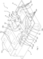
Figure 1 is a simplified schematic perspective view of a power semiconductor unit (with an insulation covering removed) with an electronic power switch drive module according to an embodiment of the invention; -
Figure 2 is a simplified schematic perspective view of an electronic power switch drive module of the embodiment offigure 1 ; -
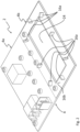
Figure 3a is a simplified schematic perspective view of an electronic power switch drive module according to another embodiment of the invention; -
Figure 3b is a simplified schematic perspective view of a portion of a power semiconductor unit comprising the electronic power switch drive module offigure 3a ; -
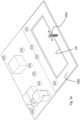
Figure 3c is a simplified schematic perspective cross sectional view of the embodiment offigure 3b ; -
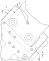
Figure 4 is a simplified schematic perspective view of a power semiconductor unit with an electronic power switch drive module according to another embodiment of the invention; -
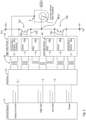
Figure 5 is a simplified block circuit diagram of a power semiconductor unit with an electronic power switch drive module according to an embodiment of the invention; -
Figure 6 is a simplified block circuit diagram of a power semiconductor unit with an electronic power switch drive module according to another embodiment of the invention; -
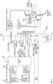
Figure 7 is a more detailed circuit diagram of an electronic power switch drive module for a power semiconductor unit, according to an embodiment of the invention. - Referring to the figures, a
power semiconductor unit 1 comprises apower semiconductor module 3 and an electronic powerswitch drive module 2 mounted and connected to the power semiconductor module. - The
power semiconductor module 3 may for instance be in the form of an insulated gate bipolar transistor (IGBT) half bridge module, comprising a power input 5 and apower output 7. The power input 5 may comprise input DC (direct current)terminals 5a-, 5a+ for connection to positive and negative conductors of a direct current supply. Thepower output 7 comprises at least oneoutput terminal 7a for at least one phase of an alternating voltage current. The waveform of the output current may have various shapes frequencies and amplitudes depending on the intended application for the power semiconductor unit. The power semiconductor unit may be implemented for use for instance in inverters for motor drives, inverters for grid connected photovoltaic plants, frequency converters for wind turbines and other power semiconductor applications. - The power semiconductor module may have two, three or more output terminals for a plurality of output phases.
- The input and output terminals may each be provided with a conductive pad and a threaded connection for a clamping bolt connection to a corresponding input or output conductor. The output conductor may for instance be in a form of a
bus bar 11 that is bolted to thecorresponding output terminal 7a. Other known interconnection means may be used such as clamping terminals, welding, soldering, plug and socket, and other per se known connection systems. - The electronic power
switch drive module 2 comprises a gate drive 6 and acurrent transducer 8. The electronic powerswitch drive module 2 comprises at least onecircuit board 4. The gate drive 6 andcurrent transducer 8 are mounted on said at least onecircuit board 4. Thecircuit board 4, or more than onecircuit board 4, comprises agate drive portion 4a and acurrent transducer portion 4b. In the illustrated embodiments, thecurrent transducer portion 4b comprises anoutput conductor passage 24 through which the conductor of thepower output 7 extends through. Thepassage 24 may be completely formed within the circuit board (as illustrated) or may only be partially surrounded (not shown) by the circuit board, for instance the circuit board may comprise a slot extending from an edge of the circuit board that forms the passage, such that the circuit board partially surrounds the passage. In the embodiments offigures 1 and2 , theoutput terminals 7a of thepower output 7 extend through thepassage 24 whereas in the embodiment offigures 3a to 3c thebus bar 11 extends through thepassage 24. Generally, the output conductor extends through thepassage 24 such that a magnetic field induced by the current flowing through the output conductor may be captured by a magnetic field sensor mounted on thecircuit board 4 adjacent and/or surrounding thepassage 24. It may be noted that the Rogowski coil sensor is best implemented surrounding the output conductor, but the discrete magnetic field sensors may be in an arrangement that is not surrounding the output conductor. The Rogowski coil sensor preferably surrounds the output conductor fully, forming an essentially closed configuration around the output conductor. In variants the rogowski coil may surround the output conductor partially, for instance if the passage is formed as a slot or indent extending from an edge of the circuit board, the Rogowski coil formed on the circuit board surrounds the output conductor partially. - It may be noted that power semiconductor modules within the scope of the invention include electronic switching devices other than IGBTs (even though these are the most common today). In this regard, the electronic power switch may be a transistor, a thyristor, or other per se known electronic power switches. The use of the term "gate" herein thus includes the conventional meaning of a transistor gate, but in the more general context of an electronic power switch is intended to take the meaning of the control input of the switch. A gate driver should thus be understood more generally as an electronic power switch driver circuit.
- The gate drive 6 comprises a circuit with circuit components that executes one or more, or all, of the following functions:
- Receive a signal from the control unit to turn on or off the switch within a given time
- Control the rise and fall times of the output voltage to comply both with constraints on power dissipation and EMI (electromagnetic interference)
- Provide fast protection of the power semiconductor switch
- Identify desaturation events by monitoring the voltage across the switch (e.g. VCE for IGBT)
- Identify overload events by monitoring the output current
- In cases where a Rogowski coil or other inductive system is used to achieve a high measurement bandwidth, this high bandwidth channel can be monitored with low latency by a local protection system to react quickly to an overload or short circuit event, as a replacement or complement or in combination with the desaturation measurement used to identify situations in which the switches need to be turned off quickly to avoid their destruction
- Provide status information to the control board to facilitate system level protection
- Monitor semiconductor switch die temperature e.g. integrated diodes
- Monitor DCB (direct copper bonded) substrate temperature e.g. through an NTC (Negative temperature coefficient) resistor
- Monitor whether local protection was triggered
- Monitor Local gate drive supply voltage
- Monitor Switching delay, by monitoring the voltage and current response to the gate drive command
- Provide information to enable condition monitoring and predictive maintenance
- Perform closed loop control of the gate drive waveform to control the output current waveform, e.g. to match the switching characteristics of paralleled modules
- Perform closed loop control of the gate drive waveform to control the slope of the output voltage to fulfill EMI and switching loss requirements
- Provide local communication to other gate drive units in the same switching "sub-unit" (the switches in a half bridge, 3 level switch, matrix, must act in concert to ensure proper operation, e.g. prevent shoot through by enforcing safeguards like dead-time.
- Implement the output side of an isolated power supply to power the GDU and current transducer.
- These functions may advantageously be effected on a
single circuit board 4 or a single circuit board potion. The connection between the gate drive 6 and thepower semiconductor module 3 is provided viainternal connections 10 that may include DC negative andpositive connections 10a-, 10a+, anNTC connection 10b, a lowside gate connection 10c, a highside emitter connection 10d, and a highside gate connection 10e. The internal connections may advantageously be provided in the form of conductive studs or bolts that ensure accurate spacing of the circuit board relative to the power semiconductor module and good electrical contact therebetween in a robust assembly. Other per se known connection techniques between thecircuit board 4 and terminals of thepower semiconductor module 3 may however be employed within the scope of the invention, for instance via soldered or welded contacts, spring contacts, press fit contacts and other per se known connection systems. - In order to reduce creepage distances and clearances, the
circuit board 4 may be overmolded or partially overmolded with an insulating material, for instance overmolded with injection or transfer molding processes to cover surface areas of the circuit board provided with conductor traces and active circuit components in a thermoplastic or thermosetting polymer. The insulating material may also comprise a potting material filled over the circuit board or potions thereof. - The electronic power switch drive module further comprises external connectors 12 for connection to external components, for instance a
signal connector 12a and apower supply connector 12b. - As best illustrated in
figure 5 , the gate drive 6 may comprise a highside drive circuit 20 and the lowside drive circuit 18 connected by aninterface circuit 22 to a semiconductordevice control board 9 of thepower semiconductor module 3 via theinternal connections 10. - The high side drive circuit and low side drive circuit may advantageously be connected to the
interface circuit 22 via anisolated connection 34. - In an embodiment illustrated in
figure 5 , the high side drive circuit and low side drive circuit are connected to theinterface 22 via inductive isolated connections 34a. Inductive isolation serves to transfer power to supply the isolated gate driver, and transfer information. Power transfer can be achieved by applying an AC voltage, in a frequency range from several kHz to several MHz, to the terminals of the primary winding of the transformer. One or several mutually isolated secondary windings can be magnetically coupled to the same primary winding, and the AC voltages appearing on the secondary side can then be rectified, filtered and regulated to produce the required DC voltages to supply the gate drive electronics. Within theinterface 22, the electronics generating the AC voltage can provide sufficient current to transfer the power required for the gate drive operation, often several Watts. The information to be transferred can be either sampled digital data, or continuous time digital data, e.g. when changing the state of a switch. The information transfer may also be based on applying an AC voltage to the primary winding, but characteristics of the AC waveform are modulated to convey information, such as the timing of a pulse edge, or the amplitude, frequency, duty cycle or phase of a pulse sequence. The modulation scheme may also have provisions to apply voltages with the sole purpose of maintaining zero average voltage at the inductor terminal. It is also possible to use a given inductively coupled circuit for bidirectional communication, e.g. in a half-duplex scheme where each side uses the same transformer alternatively, or in a sequence depending on the information transmitted. In all cases, the inductively coupled devices may be transformers with wirewound coils and magnetic cores or transformers with windings realized as PCB traces, either in the PCB of the GDU or on a separate PCB, with or without magnetic material. - In a variant illustrated in
figure 6 , the high side drive circuit and low side drive circuit are connected to theinterface 22 via digitalisolated connections 34b. While isolated power transmission is preferably realized inductively, isolated transmission of information can be realized practically with several other means in addition to inductive isolation, like optical isolation, capacitive isolation. - The high
side drive circuit 20 comprises a gatedrive circuit portion 20a driving a gate of thehigh side transistor 13a, a power supply unit (PSU) 20 and alocal protection circuit 20c. The highside circuit portion 20 may further comprise atemperature monitoring circuit 20d and adesaturation monitoring circuit 20e to measure desaturation between the collector and emitter of thetransistor 30a. The desaturation monitoring circuit may be connected to thelocal protection circuit 20c to signal a desaturation of thetransistor 13a. - A signal from the
current transducer 8 and thelocal protection circuit 20c may be fed into acontrol logic circuit 20f that is connected via acommunication circuit 20g to acontrol board 9 of the power semiconductor module. - In the illustrated embodiments, the low
side circuit portion 18 and highside circuit portion 20 are related to two-level inverters, however the invention also applies to multi-level inverters greater than two levels, whereby the lowest switch would correspond to a "low side switch" of a two level inverter, and the other switches may be considered to be on the high side, forming "high side switches" since their gate drive needs to well insulated against high dv/dt changes because their emitters are not at a constant potential. - In a two or greater level inverter, there is a "high side" switch having its emitter connected to an output potential Vout at which the output current is being measured. In the present invention, the current transducer is thus connected to at least one circuit portion of the gate drive connected to the output potential Vout at which the output current is being measured, in a non-isolated manner.
- In the embodiments illustrated, the
current transducer 8 comprises at least onemagnetic field sensor - In an advantageous embodiment, the current transducer comprises a plurality of
magnetic field sensors Rogowski coil sensor 16b mounted around theoutput conductor 7, either around theoutput terminals 7a as illustrated in the embodiment offigure 3b or around the output conductor such as theoutput bus bar 11 as illustrated in the embodiment offigure 4 . TheRogowski coil sensor 16b may comprise conductive circuit traces within or on the circuit board surrounding thepassage 24. In a preferred embodiment, the circuit traces form a Rogowski coil that fully or substantially fully surrounds thepassage 24. - The
current transducer 8 may further advantageously comprise one or a plurality of discretemagnetic field sensors 16a, for instance in a form of Hall effect sensors, mounted on the circuit board. The one or more discretemagnetic field sensors 16a mounted on thecircuit board 4, and theRogowski coil sensor 16a, allow the current transducer to have a wide frequency operating range and also enables high speed detection of an overload or fault. - In the embodiment illustrated in
figure 2 , a plurality of discretemagnetic field sensors 16a are mounted around theoutput conductor passage 24 in a spatially distributed manner, preferably in a substantially evenly distributed manner, to reduce the influence of external fields (compared to a magnetic field sensor that is not positioned in a distributed manner around the central passage) while amplifying the measurement signal. The current transducer may have two sensors, one on opposite sides of the output conductor, but preferably the current transducer comprises at least four, more preferably six, eight or more spaced apart and substantially evenly distributed discrete magnetic field sensors around theoutput conductor passage 24. - As illustrated in the
figures 3a to 3c , in a variant, the discrete magnetic field sensor may comprise a magnetic field gradient sensor that is inserted in a cavity ororifice 15 in theoutput conductor 11. The magnetic field gradient sensor may for instance comprise or consist in a pair of oppositely arranged Hall sensors configured to measure a gradient of the magnetic field generated by the output current flowing in the output conductor. The functioning principle of a magnetic field gradient sensor to measure a primary current is per se known and shall not be further described herein. - In the illustrated embodiment, the magnetic
field gradient sensor 16a' may advantageously be mounted on thecircuit board 4 that is positioned below thebus bar 11 for a simple and economical assembly of the various components. - As illustrated in embodiment
figure 4 , theRogowski coil 16b may be mounted on acircuit board portion 4b that is separate from the gate drivecircuit board portion 4a, connected thereto for instance by a flexible connectingcable 32 or other form of electrical interconnect. In the illustrated embodiment offigure 4 , the current transducercircuit board portion 4b is arranged orthogonal to the gate drivecircuit board portion 4a, but the skilled person will appreciate that thecircuit board portion 4b may be arranged parallel to the gate drive circuit board portion or at any other angle or disposition depending on the geometry of the output conductor arrangement. In thefigure 4 illustrated embodiment, the separatecircuit board portion 4b comprising the full current transducer, includes a main portion orthogonal to the gate drivecircuit board portion 4a and a complementarycircuit board portion 4b' orthogonal to themain portion 4b and carrying the discrete magnetic field sensor, for instance a gradient magnetic field sensor inserted in an orifice in theoutput conductor bar 11. In a variant, the discrete magnetic field sensors may be mounted on thecircuit board portion 4b, surrounding theoutput conductor bar 11. - The Rogowski coil
magnetic field sensor 16b and discrete magnetic field sensor(s) 16a, 16a' are interconnected to asignal processing circuit 30 for generating a measurement of the output current from one or both of the current sensors as function of the operating frequency and/or current amplitude. A plurality of discretemagnetic field sensors 16a may be connected to a summingcircuit 30a, as is per se known in the art, to generate the measurement of the magnetic field representative of the output current. The output signals of the plurality of discrete magnetic field sensors may be processed for instance to generate a weighted sum corresponding to a signal proportional to the measured current. - Advantageously, the current transducer combined with the gate drive in an electronic power switch drive module directly connected to the power semiconductor module enables a fast and low loss control of the semiconductor power device with feedback from the output. The non-isolated current transducer within the electronic power switch drive modules reduces the number of components (compared to an external current transducer) and removes the need for isolation, whereby the current transducer may be supplied with the same power supply as the high side drive of the electronic power switch drive module. Direct integration of the current transducer within the drive control unit also enables very fast response in case of fault or overload thus forming excellent overcurrent protection.
- It may be noted that the magnetic field detectors employed within the scope of the invention may comprise various magnetic field sensors and combinations of magnetic field sensors such as fluxgate and magnetoresistive sensors, and may include soft magnetic elements to concentrate or change the direction of impinging magnetic fields. Such magnetic elements may be realized as macroscopic parts placed at the PCB level, or integrated in a package, or realized with a wafer level process as integrated magnetic concentrators. The magnetic field sensors may include systems to operate with a local feedback coil resulting in near zero flux operation to compensate for sensitivity variations and nonlinearities. The field magnetic sensors may measure the magnetic field in a direction perpendicular to the plane of the substrate or parallel to the plane of the substrate, and be mounted accordingly in packages to be soldered on a PCB, or as semiconductor dies embedded inside a the PCB.
- The isolated transmission of the current measurement data to the power semiconductor unit control board may implement inductive, capacitive, radio, or optical transmission technologies, and can be either a dedicated isolator carrying only this information or a take place over an isolator used to transmit a combination of data back to the control unit. This information can include gate supply voltage, VCE, status of protection circuits, current, temperatures (e.g. if temperature is available per chip in addition of per IGBT module). Various information and data may be combined (e.g. into a frame) and transmitted over a single isolated channel. This combination may be performed by a logic circuit, e.g. a microcontroller, DSP, FPGA or CPLD, that may perform this and other functions associated with the gate drive unit.
- Advantages of the proposed invention include :
- low dissipation
- good frequency response (compared to di/dt component in low value shunts caused by parasitic mutual inductances)
- no thermoelectric offset (compared to shunt resistors with low full scale output voltage)
- no magnetic core losses, no hysteresis, low mass
- for the magnetic field gradient sensor variant : low consumption, low cost
- for the combined magnetic field gradient sensor and full PCB Rogowski coil: avoid frequency response issues of pure gradient sensor due to skin and proximity effect resulting in frequency dependent changes in current density distribution, which result in varying magnetic coupling with the gradient sensor and changes in sensitivity
- Isolation (housing, potting) and countering dv/dt from the voltage swing of the output bus bar (e.g. in the form of shielding, differential transmission, receivers with high CM immunity) are cost drivers for a current transducer. Digital data transmission is however economical, and it is thus an advantage to combine the low insertion loss advantage of a magnetically coupled current transducer with the low isolation cost and elimination of dv/dt effects of digital isolation.
- In addition, a Rogowski coil has a low power supply requirement, enabling a supply through the isolated gate driver power supply, making it easier to interconnect than previous separate transducer arrangements.
- The combined gate drive and current transducer in a single device facilitates bus bar design, system design and enables system level cost savings for the power semiconductor unit.
- Moreover, fast current measurement with a Rogowski coil sensor enables effective overcurrent protection schemes and closed loop control of transistor switching.
-
Power semiconductor unit 1
(e.g. insulated gate bipolar transistor IGBT assembly) -
Semiconductor Module 3
(e.g. IGBT half bridge module)- Input 5
Input DC terminals -ve, +ve 5a-, 5a+ -
Output 7
Output terminals 7a -
Bus bar 11
Sensor Cavity 15 - Semiconductor
device control board 9 -
Electronic power switch - (
e.g Transistor
- Input 5
- Electronic power switch
drive control module 2 - (e.g. Gate drive control module 2)
-
Circuit board 4- Electronic power
switch drive portion 4a - (e.g.
Gate drive portion 4a) -
Current transducer portion 4b -
Output conductor passage 24 - Interconnection 32 (e.g. flex cable)
- Electronic power
- Electronic power switch drive 6
- (e.g. Gate Drive 6)
-
Internal connections 10- DC -ve, +ve
connections 10a-, 10a+ -
NTC connection 10b - Low
side gate connection 10c - High
side emitter connection 10d - High
side gate connection 10e
- DC -ve, +ve
- External connectors 12
-
Signal connector 12a -
Power supply connector 12b
-
- Circuit components
Transformer 14 - Circuit portion(s) 18, 20
- First (e.g Low side)
circuit portion 18- Drive
circuit 18a - Power supply (PSU) 18b
- Local protection circuit 18c
- Drive
- Second (e.g. High side)
circuit portion 20- Drive
circuit 20a - Power supply (PSU) 20b
-
Local protection circuit 20c -
Temperature monitoring circuit 20d -
Desaturation monitoring circuit 20e -
Control logic circuit 20f -
Communication circuit 20g- Transmitter (Serializer, isolated data transmitter)
- Receiver (Deserializer, isolated data transmitter)
-
Connection isolator 34-
Digital connection isolator 34b - Inductive connection isolator 34a
-
- Drive
- First (e.g Low side)
-
Interface 22
-
-
Current transducer 8- Magnetic field Sensors
-
Hall effect sensor 16a
Gradient sensor 16a' - Rogowski coil sensor (PCB Rogowski coil) 16b
-
Signal processing circuit 30
Summingcircuit 30a
-
Claims (12)
- An electronic power switch drive control module (2) for a power semiconductor unit (1), comprising an electronic power switch drive (6) and a current transducer (8) mounted on one or more circuit boards (4), the electronic power switch drive comprising at least one circuit portion (20) for controlling at least one electronic power switch (13a) of a power semiconductor module (3) of said power semiconductor unit (1), the current transducer (8) configured to be coupled to an output (7) of the power semiconductor module (3) for measuring an output current of the power semiconductor module, said at least one circuit portion (20) being a high side drive circuit connected to an output potential ( Vout) of the output current to be measured, said electronic power switch drive (6) further comprising a low side drive circuit (18), the current transducer comprises a Rogowski coil (16b) surrounding a passage (24) formed in a current transducer portion (4b) of said one or more circuit boards, the passage configured for extension of an output conductor of the power semiconductor module therethrough, and at least one discrete magnetic field sensor (16a, 16a') mounted on said current transducer portion (4b), the current transducer being connected to said at least one high side drive circuit of the electronic power switch drive at said output potential in a non-isolated manner, said at least one high side drive circuit comprising a control logic circuit (20f) configured for connection to a control board (9) of said power semiconductor module (3), a measurement output signal of the current transducer being fed into the control logic circuit, said high side drive circuit (20) and low side drive circuit (18) connected via an isolated connection (34) to an interface circuit (22) connected to said control board (9), and wherein the current transducer comprises a signal processing circuit (30) connected to the Rogowski coil magnetic field sensor and to the at least one discrete magnetic field sensor, the signal processing circuit combining the signal of the Rogowski magnetic field sensor and the at least one discrete magnetic field sensor for generating a measurement signal of the output current.
- The electronic power switch drive module according to claim 1 wherein said electronic power switch drive is a transistor gate drive (6) and said at least one electronic power switch is a transistor (13a).
- The electronic power switch drive module according to any preceding claim wherein the current transducer comprises a plurality of discrete magnetic field sensors mounted on a portion of the circuit board surrounding a passage (24) formed in the portion circuit board configured for receiving therethrough the output conductor (7).
- The electronic power switch drive module according to any preceding claim wherein at least one of the said discrete magnetic fields sensors is a magnetic field gradient sensor.
- The electronic power switch drive module according to any preceding claim wherein the discrete magnetic field sensor is a Hall effect sensor.
- The electronic power switch drive module according to any preceding claim wherein the electronic power switch drive module comprises a single circuit board on which both the gate drive circuit and current transducer are mounted.
- The electronic power switch drive module according to any preceding claim comprising connection studs for connecting the electronic power switch drive module (2) to the power semiconductor module (3).
- The electronic power switch drive module according to any preceding claim comprising a signal or data communication interface (20g) for connection to a control unit of the power semiconductor unit (1).
- The electronic power switch drive module according to any preceding claim wherein said at least one circuit portion (20) comprises a local protection circuit (20c) connected to an output of the current transducer (8), the local protection circuit connected to drive circuits of transistors (13a, 13b) of the power semiconductor module (3).
- The electronic power switch drive module according to any preceding claim wherein the gate drive circuit (6) comprises an isolated connection (34) to said interface circuit (22) for data, power or both data and power connection to the power semiconductor module (3).
- A power semiconductor unit (1) comprising an electronic power switch drive module (2) according to any preceding claim and a power semiconductor module (3), the electronic power switch drive module being mounted on the power semiconductor module (3) wherein the power semiconductor unit is an IGBT device.
- The power semiconductor unit according to the preceding claim comprising direct current input terminals (5a-, 5a+) on one end of the power semiconductor unit (1) and output terminals (7a) arranged on an opposite end of the power semiconductor unit (1), the electronic power switch drive module (2) being mounted on the power semiconductor module (3) between the input terminals and output terminals.
Applications Claiming Priority (2)
| Application Number | Priority Date | Filing Date | Title |
|---|---|---|---|
| EP18159316.1A EP3534538A1 (en) | 2018-02-28 | 2018-02-28 | Electronic power switch drive module |
| PCT/EP2019/054788 WO2019166455A2 (en) | 2018-02-28 | 2019-02-27 | Electronic power switch drive module |
Publications (3)
| Publication Number | Publication Date |
|---|---|
| EP3759819A2 EP3759819A2 (en) | 2021-01-06 |
| EP3759819B1 true EP3759819B1 (en) | 2025-03-19 |
| EP3759819C0 EP3759819C0 (en) | 2025-03-19 |
Family
ID=61557060
Family Applications (2)
| Application Number | Title | Priority Date | Filing Date |
|---|---|---|---|
| EP18159316.1A Withdrawn EP3534538A1 (en) | 2018-02-28 | 2018-02-28 | Electronic power switch drive module |
| EP19706682.2A Active EP3759819B1 (en) | 2018-02-28 | 2019-02-27 | Electronic power switch drive module |
Family Applications Before (1)
| Application Number | Title | Priority Date | Filing Date |
|---|---|---|---|
| EP18159316.1A Withdrawn EP3534538A1 (en) | 2018-02-28 | 2018-02-28 | Electronic power switch drive module |
Country Status (5)
| Country | Link |
|---|---|
| US (1) | US11955958B2 (en) |
| EP (2) | EP3534538A1 (en) |
| JP (1) | JP7230048B2 (en) |
| CN (1) | CN111886802B (en) |
| WO (1) | WO2019166455A2 (en) |
Families Citing this family (13)
| Publication number | Priority date | Publication date | Assignee | Title |
|---|---|---|---|---|
| JP6791180B2 (en) * | 2018-03-01 | 2020-11-25 | Tdk株式会社 | Sensor |
| DE102019102567B3 (en) * | 2019-02-01 | 2020-03-05 | Dr. Ing. H.C. F. Porsche Aktiengesellschaft | Sensor device for measuring direct and alternating currents |
| US11571803B2 (en) | 2019-05-30 | 2023-02-07 | Milwaukee Electric Tool Corporation | Power tool with combined chip for wireless communications and power tool control |
| EP3982404A1 (en) * | 2020-10-07 | 2022-04-13 | Infineon Technologies Austria AG | Semiconductor module |
| US20240098927A1 (en) * | 2020-12-07 | 2024-03-21 | Valeo Eautomotive Germany Gmbh | Electrical device, inverter, electric drive, vehicle and manufacturing methods |
| JP7767750B2 (en) * | 2021-06-30 | 2025-11-12 | 富士電機株式会社 | Integrated circuits and power modules |
| DE102021211423A1 (en) * | 2021-10-11 | 2023-04-13 | Robert Bosch Gesellschaft mit beschränkter Haftung | Inverter for an electric machine |
| DE102022100034B3 (en) * | 2022-01-03 | 2023-05-04 | Infineon Technologies Ag | POWER ELECTRONIC SYSTEM, METHOD OF MAKING A POWER ELECTRONIC SYSTEM AND METHOD OF PROTECTING A HALF-BRIDGE CIRCUIT AGAINST OVERLOAD OR OVERCURRENT |
| EP4210209A1 (en) | 2022-01-10 | 2023-07-12 | Hamilton Sundstrand Corporation | Current detection in electrical power converters |
| KR102521738B1 (en) * | 2023-03-14 | 2023-04-17 | (주)에너담 | Non-Powered Switch Type Current Sensor |
| JP2024147883A (en) * | 2023-04-04 | 2024-10-17 | ミネベアパワーデバイス株式会社 | Power conversion device, overcurrent detection circuit, and semiconductor module |
| EP4443735A1 (en) * | 2023-04-06 | 2024-10-09 | Hamilton Sundstrand Corporation | Multilevel power converter |
| CN118353365A (en) * | 2024-03-11 | 2024-07-16 | 华为数字能源技术有限公司 | Power backup device and photovoltaic system |
Citations (1)
| Publication number | Priority date | Publication date | Assignee | Title |
|---|---|---|---|---|
| US6366076B1 (en) * | 1997-04-21 | 2002-04-02 | Liaisons Electroniques-Mecaniques Lem Sa | Device with wide passband for measuring electric current intensity in a conductor |
Family Cites Families (18)
| Publication number | Priority date | Publication date | Assignee | Title |
|---|---|---|---|---|
| JPH0729739Y2 (en) * | 1989-01-06 | 1995-07-05 | 株式会社三陽電機製作所 | FET drive circuit |
| JP2979930B2 (en) * | 1993-10-28 | 1999-11-22 | 富士電機株式会社 | Power semiconductor device package |
| JP2001045741A (en) * | 1999-08-03 | 2001-02-16 | Hitachi Ltd | Power conversion device using hard drive GTO |
| JP4731418B2 (en) * | 2006-07-10 | 2011-07-27 | 三菱電機株式会社 | Semiconductor module |
| JP5029900B2 (en) * | 2007-11-20 | 2012-09-19 | アイシン・エィ・ダブリュ株式会社 | Motor control device |
| CN103392067B (en) * | 2011-01-21 | 2016-02-24 | 维斯塔斯风力系统集团公司 | Wind turbine fault detection circuit and method |
| JP5508357B2 (en) * | 2011-07-29 | 2014-05-28 | 日立オートモティブシステムズ株式会社 | Power converter |
| JP5928430B2 (en) * | 2013-10-03 | 2016-06-01 | トヨタ自動車株式会社 | Current sensor, power converter |
| EP2955849A1 (en) * | 2014-06-11 | 2015-12-16 | CT-Concept Technologie GmbH | Device for generating a dynamic reference signal for a driver circuit for a semiconductor power switch |
| DE102015009092A1 (en) * | 2014-07-18 | 2016-01-21 | Technische Universität Braunschweig | Device and method for current measurement |
| GB2534348A (en) * | 2014-11-21 | 2016-07-27 | Reinhausen Maschf Scheubeck | Active Snubber |
| DE102015205794A1 (en) * | 2015-03-31 | 2016-10-06 | Siemens Aktiengesellschaft | Current measuring device and method for determining an electric current |
| DE102015105192A1 (en) * | 2015-04-04 | 2016-10-06 | Sma Solar Technology Ag | Driver circuit, circuit arrangement comprising a driver circuit and inverter comprising a circuit arrangement |
| KR101721107B1 (en) * | 2015-07-15 | 2017-03-29 | 엘에스산전 주식회사 | Gate driver circuit for power switching device |
| JP2017092670A (en) * | 2015-11-09 | 2017-05-25 | 三菱電機株式会社 | Pulse generation device |
| JP6769707B2 (en) * | 2015-12-03 | 2020-10-14 | ローム株式会社 | Semiconductor module |
| JP2017158407A (en) * | 2016-03-04 | 2017-09-07 | 日本特殊陶業株式会社 | Current controller for power conversion system |
| EP3229373A1 (en) * | 2016-04-06 | 2017-10-11 | Volke Andreas | Soft shutdown modular circuitry for power semiconductor switches |
-
2018
- 2018-02-28 EP EP18159316.1A patent/EP3534538A1/en not_active Withdrawn
-
2019
- 2019-02-27 JP JP2020545113A patent/JP7230048B2/en active Active
- 2019-02-27 CN CN201980015919.9A patent/CN111886802B/en active Active
- 2019-02-27 EP EP19706682.2A patent/EP3759819B1/en active Active
- 2019-02-27 WO PCT/EP2019/054788 patent/WO2019166455A2/en not_active Ceased
- 2019-02-27 US US16/976,352 patent/US11955958B2/en active Active
Patent Citations (1)
| Publication number | Priority date | Publication date | Assignee | Title |
|---|---|---|---|---|
| US6366076B1 (en) * | 1997-04-21 | 2002-04-02 | Liaisons Electroniques-Mecaniques Lem Sa | Device with wide passband for measuring electric current intensity in a conductor |
Also Published As
| Publication number | Publication date |
|---|---|
| WO2019166455A3 (en) | 2019-10-31 |
| US20210006240A1 (en) | 2021-01-07 |
| JP2021515518A (en) | 2021-06-17 |
| JP7230048B2 (en) | 2023-02-28 |
| EP3759819A2 (en) | 2021-01-06 |
| US11955958B2 (en) | 2024-04-09 |
| EP3759819C0 (en) | 2025-03-19 |
| CN111886802A (en) | 2020-11-03 |
| EP3534538A1 (en) | 2019-09-04 |
| WO2019166455A2 (en) | 2019-09-06 |
| CN111886802B (en) | 2024-05-28 |
Similar Documents
| Publication | Publication Date | Title |
|---|---|---|
| US11955958B2 (en) | Electronic power switch drive module | |
| Anurag et al. | Design considerations and development of an innovative gate driver for medium-voltage power devices with high $ dv/dt$ | |
| US7622887B2 (en) | Power electronics equipments | |
| US8288894B2 (en) | Power electronics equipment for transmitting signals to switching devices through air-cored insulating transformer | |
| JP6444591B2 (en) | Integrated circuit package | |
| US10134718B2 (en) | Power semiconductor module | |
| US20080266042A1 (en) | Transformer unit, and power converting device | |
| JP2014099610A (en) | Integrated circuit package and switch mode power converter | |
| Hasegawa et al. | A new output current measurement method with tiny PCB sensors capable of being embedded in an IGBT module | |
| CN110999055B (en) | System and method for fast current sensing and transistor timing control | |
| Onar et al. | A SiC MOSFET based inverter for wireless power transfer applications | |
| EP4187585A2 (en) | Power module with integrated gate driver and functional components within a single power module housing | |
| Lobsiger et al. | Decentralized active gate control for current balancing of parallel connected IGBT modules | |
| JP5796599B2 (en) | Semiconductor module and switching element drive device | |
| KR101998434B1 (en) | Current measuring device and method for operating a current measuring device | |
| CN107710580B (en) | Circuit arrangement for fast switching of a converter | |
| JP6766965B2 (en) | Power converter | |
| CN208143591U (en) | Motor drive | |
| US6411109B1 (en) | Connecting lug used as a current-sense resistor | |
| Nibir et al. | Investigations on circuits and layout for non-intrusive switch current measurements in high frequency converters using parallel GaN HEMTs | |
| CN224069038U (en) | DPIM half-bridge power module | |
| EP3435543A1 (en) | A semiconductor device and method of measurement of physical parameters of a semiconductor device | |
| US20240379512A1 (en) | Semiconductor device | |
| EP4742536A1 (en) | Power control apparatus | |
| Mishra et al. | Evaluation of All SiC MOSFET Based Voltage Source Inverter with Open Loop Induction Motor |
Legal Events
| Date | Code | Title | Description |
|---|---|---|---|
| STAA | Information on the status of an ep patent application or granted ep patent |
Free format text: STATUS: UNKNOWN |
|
| STAA | Information on the status of an ep patent application or granted ep patent |
Free format text: STATUS: THE INTERNATIONAL PUBLICATION HAS BEEN MADE |
|
| PUAI | Public reference made under article 153(3) epc to a published international application that has entered the european phase |
Free format text: ORIGINAL CODE: 0009012 |
|
| STAA | Information on the status of an ep patent application or granted ep patent |
Free format text: STATUS: REQUEST FOR EXAMINATION WAS MADE |
|
| 17P | Request for examination filed |
Effective date: 20200901 |
|
| AK | Designated contracting states |
Kind code of ref document: A2 Designated state(s): AL AT BE BG CH CY CZ DE DK EE ES FI FR GB GR HR HU IE IS IT LI LT LU LV MC MK MT NL NO PL PT RO RS SE SI SK SM TR |
|
| AX | Request for extension of the european patent |
Extension state: BA ME |
|
| DAV | Request for validation of the european patent (deleted) | ||
| DAX | Request for extension of the european patent (deleted) | ||
| STAA | Information on the status of an ep patent application or granted ep patent |
Free format text: STATUS: EXAMINATION IS IN PROGRESS |
|
| 17Q | First examination report despatched |
Effective date: 20220908 |
|
| RAP3 | Party data changed (applicant data changed or rights of an application transferred) |
Owner name: LEM INTERNATIONAL SA |
|
| GRAP | Despatch of communication of intention to grant a patent |
Free format text: ORIGINAL CODE: EPIDOSNIGR1 |
|
| STAA | Information on the status of an ep patent application or granted ep patent |
Free format text: STATUS: GRANT OF PATENT IS INTENDED |
|
| INTG | Intention to grant announced |
Effective date: 20241219 |
|
| RIN1 | Information on inventor provided before grant (corrected) |
Inventor name: TROMBERT, STEPHAN Inventor name: SCHLAEFLI, DOMINIK |
|
| GRAS | Grant fee paid |
Free format text: ORIGINAL CODE: EPIDOSNIGR3 |
|
| GRAA | (expected) grant |
Free format text: ORIGINAL CODE: 0009210 |
|
| STAA | Information on the status of an ep patent application or granted ep patent |
Free format text: STATUS: THE PATENT HAS BEEN GRANTED |
|
| AK | Designated contracting states |
Kind code of ref document: B1 Designated state(s): AL AT BE BG CH CY CZ DE DK EE ES FI FR GB GR HR HU IE IS IT LI LT LU LV MC MK MT NL NO PL PT RO RS SE SI SK SM TR |
|
| REG | Reference to a national code |
Ref country code: GB Ref legal event code: FG4D |
|
| REG | Reference to a national code |
Ref country code: CH Ref legal event code: EP |
|
| REG | Reference to a national code |
Ref country code: IE Ref legal event code: FG4D |
|
| REG | Reference to a national code |
Ref country code: DE Ref legal event code: R096 Ref document number: 602019067443 Country of ref document: DE |
|
| U01 | Request for unitary effect filed |
Effective date: 20250319 |
|
| U07 | Unitary effect registered |
Designated state(s): AT BE BG DE DK EE FI FR IT LT LU LV MT NL PT RO SE SI Effective date: 20250325 |
|
| PG25 | Lapsed in a contracting state [announced via postgrant information from national office to epo] |
Ref country code: RS Free format text: LAPSE BECAUSE OF FAILURE TO SUBMIT A TRANSLATION OF THE DESCRIPTION OR TO PAY THE FEE WITHIN THE PRESCRIBED TIME-LIMIT Effective date: 20250619 |
|
| PG25 | Lapsed in a contracting state [announced via postgrant information from national office to epo] |
Ref country code: NO Free format text: LAPSE BECAUSE OF FAILURE TO SUBMIT A TRANSLATION OF THE DESCRIPTION OR TO PAY THE FEE WITHIN THE PRESCRIBED TIME-LIMIT Effective date: 20250619 |
|
| PG25 | Lapsed in a contracting state [announced via postgrant information from national office to epo] |
Ref country code: HR Free format text: LAPSE BECAUSE OF FAILURE TO SUBMIT A TRANSLATION OF THE DESCRIPTION OR TO PAY THE FEE WITHIN THE PRESCRIBED TIME-LIMIT Effective date: 20250319 |
|
| PG25 | Lapsed in a contracting state [announced via postgrant information from national office to epo] |
Ref country code: GR Free format text: LAPSE BECAUSE OF FAILURE TO SUBMIT A TRANSLATION OF THE DESCRIPTION OR TO PAY THE FEE WITHIN THE PRESCRIBED TIME-LIMIT Effective date: 20250620 |
|
| PG25 | Lapsed in a contracting state [announced via postgrant information from national office to epo] |
Ref country code: SM Free format text: LAPSE BECAUSE OF FAILURE TO SUBMIT A TRANSLATION OF THE DESCRIPTION OR TO PAY THE FEE WITHIN THE PRESCRIBED TIME-LIMIT Effective date: 20250319 |
|
| PG25 | Lapsed in a contracting state [announced via postgrant information from national office to epo] |
Ref country code: ES Free format text: LAPSE BECAUSE OF FAILURE TO SUBMIT A TRANSLATION OF THE DESCRIPTION OR TO PAY THE FEE WITHIN THE PRESCRIBED TIME-LIMIT Effective date: 20250319 |
|
| PG25 | Lapsed in a contracting state [announced via postgrant information from national office to epo] |
Ref country code: PL Free format text: LAPSE BECAUSE OF FAILURE TO SUBMIT A TRANSLATION OF THE DESCRIPTION OR TO PAY THE FEE WITHIN THE PRESCRIBED TIME-LIMIT Effective date: 20250319 |
|
| PG25 | Lapsed in a contracting state [announced via postgrant information from national office to epo] |
Ref country code: CZ Free format text: LAPSE BECAUSE OF FAILURE TO SUBMIT A TRANSLATION OF THE DESCRIPTION OR TO PAY THE FEE WITHIN THE PRESCRIBED TIME-LIMIT Effective date: 20250319 |
|
| PG25 | Lapsed in a contracting state [announced via postgrant information from national office to epo] |
Ref country code: SK Free format text: LAPSE BECAUSE OF FAILURE TO SUBMIT A TRANSLATION OF THE DESCRIPTION OR TO PAY THE FEE WITHIN THE PRESCRIBED TIME-LIMIT Effective date: 20250319 |
|
| PG25 | Lapsed in a contracting state [announced via postgrant information from national office to epo] |
Ref country code: IS Free format text: LAPSE BECAUSE OF FAILURE TO SUBMIT A TRANSLATION OF THE DESCRIPTION OR TO PAY THE FEE WITHIN THE PRESCRIBED TIME-LIMIT Effective date: 20250719 |
|
| PLBE | No opposition filed within time limit |
Free format text: ORIGINAL CODE: 0009261 |
|
| STAA | Information on the status of an ep patent application or granted ep patent |
Free format text: STATUS: NO OPPOSITION FILED WITHIN TIME LIMIT |
|
| REG | Reference to a national code |
Ref country code: CH Ref legal event code: L10 Free format text: ST27 STATUS EVENT CODE: U-0-0-L10-L00 (AS PROVIDED BY THE NATIONAL OFFICE) Effective date: 20260128 |
|
| 26N | No opposition filed |
Effective date: 20251222 |
|
| U20 | Renewal fee for the european patent with unitary effect paid |
Year of fee payment: 8 Effective date: 20260122 |
|
| REG | Reference to a national code |
Ref country code: CH Ref legal event code: U11 Free format text: ST27 STATUS EVENT CODE: U-0-0-U10-U11 (AS PROVIDED BY THE NATIONAL OFFICE) Effective date: 20260301 |
|
| PGFP | Annual fee paid to national office [announced via postgrant information from national office to epo] |
Ref country code: CH Payment date: 20260301 Year of fee payment: 8 |