EP3759651B1 - Carte à puce sans contact à modules électroniques multiples communicants - Google Patents
Carte à puce sans contact à modules électroniques multiples communicants Download PDFInfo
- Publication number
- EP3759651B1 EP3759651B1 EP19711955.5A EP19711955A EP3759651B1 EP 3759651 B1 EP3759651 B1 EP 3759651B1 EP 19711955 A EP19711955 A EP 19711955A EP 3759651 B1 EP3759651 B1 EP 3759651B1
- Authority
- EP
- European Patent Office
- Prior art keywords
- module
- modules
- optical
- electronic
- chip
- Prior art date
- Legal status (The legal status is an assumption and is not a legal conclusion. Google has not performed a legal analysis and makes no representation as to the accuracy of the status listed.)
- Active
Links
Images


Classifications
-
- G—PHYSICS
- G06—COMPUTING OR CALCULATING; COUNTING
- G06K—GRAPHICAL DATA READING; PRESENTATION OF DATA; RECORD CARRIERS; HANDLING RECORD CARRIERS
- G06K19/00—Record carriers for use with machines and with at least a part designed to carry digital markings
- G06K19/06—Record carriers for use with machines and with at least a part designed to carry digital markings characterised by the kind of the digital marking, e.g. shape, nature, code
- G06K19/067—Record carriers with conductive marks, printed circuits or semiconductor circuit elements, e.g. credit or identity cards also with resonating or responding marks without active components
- G06K19/07—Record carriers with conductive marks, printed circuits or semiconductor circuit elements, e.g. credit or identity cards also with resonating or responding marks without active components with integrated circuit chips
- G06K19/0723—Record carriers with conductive marks, printed circuits or semiconductor circuit elements, e.g. credit or identity cards also with resonating or responding marks without active components with integrated circuit chips the record carrier comprising an arrangement for non-contact communication, e.g. wireless communication circuits on transponder cards, non-contact smart cards or RFIDs
- G06K19/0728—Record carriers with conductive marks, printed circuits or semiconductor circuit elements, e.g. credit or identity cards also with resonating or responding marks without active components with integrated circuit chips the record carrier comprising an arrangement for non-contact communication, e.g. wireless communication circuits on transponder cards, non-contact smart cards or RFIDs the arrangement being an optical or sound-based communication interface
-
- G—PHYSICS
- G06—COMPUTING OR CALCULATING; COUNTING
- G06K—GRAPHICAL DATA READING; PRESENTATION OF DATA; RECORD CARRIERS; HANDLING RECORD CARRIERS
- G06K19/00—Record carriers for use with machines and with at least a part designed to carry digital markings
- G06K19/06—Record carriers for use with machines and with at least a part designed to carry digital markings characterised by the kind of the digital marking, e.g. shape, nature, code
- G06K19/067—Record carriers with conductive marks, printed circuits or semiconductor circuit elements, e.g. credit or identity cards also with resonating or responding marks without active components
- G06K19/07—Record carriers with conductive marks, printed circuits or semiconductor circuit elements, e.g. credit or identity cards also with resonating or responding marks without active components with integrated circuit chips
- G06K19/0716—Record carriers with conductive marks, printed circuits or semiconductor circuit elements, e.g. credit or identity cards also with resonating or responding marks without active components with integrated circuit chips at least one of the integrated circuit chips comprising a sensor or an interface to a sensor
- G06K19/0718—Record carriers with conductive marks, printed circuits or semiconductor circuit elements, e.g. credit or identity cards also with resonating or responding marks without active components with integrated circuit chips at least one of the integrated circuit chips comprising a sensor or an interface to a sensor the sensor being of the biometric kind, e.g. fingerprint sensors
-
- G—PHYSICS
- G06—COMPUTING OR CALCULATING; COUNTING
- G06K—GRAPHICAL DATA READING; PRESENTATION OF DATA; RECORD CARRIERS; HANDLING RECORD CARRIERS
- G06K19/00—Record carriers for use with machines and with at least a part designed to carry digital markings
- G06K19/06—Record carriers for use with machines and with at least a part designed to carry digital markings characterised by the kind of the digital marking, e.g. shape, nature, code
- G06K19/067—Record carriers with conductive marks, printed circuits or semiconductor circuit elements, e.g. credit or identity cards also with resonating or responding marks without active components
- G06K19/07—Record carriers with conductive marks, printed circuits or semiconductor circuit elements, e.g. credit or identity cards also with resonating or responding marks without active components with integrated circuit chips
- G06K19/0723—Record carriers with conductive marks, printed circuits or semiconductor circuit elements, e.g. credit or identity cards also with resonating or responding marks without active components with integrated circuit chips the record carrier comprising an arrangement for non-contact communication, e.g. wireless communication circuits on transponder cards, non-contact smart cards or RFIDs
-
- G—PHYSICS
- G06—COMPUTING OR CALCULATING; COUNTING
- G06K—GRAPHICAL DATA READING; PRESENTATION OF DATA; RECORD CARRIERS; HANDLING RECORD CARRIERS
- G06K19/00—Record carriers for use with machines and with at least a part designed to carry digital markings
- G06K19/06—Record carriers for use with machines and with at least a part designed to carry digital markings characterised by the kind of the digital marking, e.g. shape, nature, code
- G06K19/067—Record carriers with conductive marks, printed circuits or semiconductor circuit elements, e.g. credit or identity cards also with resonating or responding marks without active components
- G06K19/07—Record carriers with conductive marks, printed circuits or semiconductor circuit elements, e.g. credit or identity cards also with resonating or responding marks without active components with integrated circuit chips
- G06K19/073—Special arrangements for circuits, e.g. for protecting identification code in memory
- G06K19/07309—Means for preventing undesired reading or writing from or onto record carriers
- G06K19/07345—Means for preventing undesired reading or writing from or onto record carriers by activating or deactivating at least a part of the circuit on the record carrier, e.g. ON/OFF switches
- G06K19/07354—Means for preventing undesired reading or writing from or onto record carriers by activating or deactivating at least a part of the circuit on the record carrier, e.g. ON/OFF switches by biometrically sensitive means, e.g. fingerprint sensitive
-
- G—PHYSICS
- G06—COMPUTING OR CALCULATING; COUNTING
- G06K—GRAPHICAL DATA READING; PRESENTATION OF DATA; RECORD CARRIERS; HANDLING RECORD CARRIERS
- G06K19/00—Record carriers for use with machines and with at least a part designed to carry digital markings
- G06K19/06—Record carriers for use with machines and with at least a part designed to carry digital markings characterised by the kind of the digital marking, e.g. shape, nature, code
- G06K19/067—Record carriers with conductive marks, printed circuits or semiconductor circuit elements, e.g. credit or identity cards also with resonating or responding marks without active components
- G06K19/07—Record carriers with conductive marks, printed circuits or semiconductor circuit elements, e.g. credit or identity cards also with resonating or responding marks without active components with integrated circuit chips
- G06K19/077—Constructional details, e.g. mounting of circuits in the carrier
- G06K19/07745—Mounting details of integrated circuit chips
- G06K19/07747—Mounting details of integrated circuit chips at least one of the integrated circuit chips being mounted as a module
-
- G—PHYSICS
- G06—COMPUTING OR CALCULATING; COUNTING
- G06K—GRAPHICAL DATA READING; PRESENTATION OF DATA; RECORD CARRIERS; HANDLING RECORD CARRIERS
- G06K19/00—Record carriers for use with machines and with at least a part designed to carry digital markings
- G06K19/06—Record carriers for use with machines and with at least a part designed to carry digital markings characterised by the kind of the digital marking, e.g. shape, nature, code
- G06K19/067—Record carriers with conductive marks, printed circuits or semiconductor circuit elements, e.g. credit or identity cards also with resonating or responding marks without active components
- G06K19/07—Record carriers with conductive marks, printed circuits or semiconductor circuit elements, e.g. credit or identity cards also with resonating or responding marks without active components with integrated circuit chips
- G06K19/077—Constructional details, e.g. mounting of circuits in the carrier
- G06K19/07749—Constructional details, e.g. mounting of circuits in the carrier the record carrier being capable of non-contact communication, e.g. constructional details of the antenna of a non-contact smart card
-
- G—PHYSICS
- G06—COMPUTING OR CALCULATING; COUNTING
- G06K—GRAPHICAL DATA READING; PRESENTATION OF DATA; RECORD CARRIERS; HANDLING RECORD CARRIERS
- G06K19/00—Record carriers for use with machines and with at least a part designed to carry digital markings
- G06K19/06—Record carriers for use with machines and with at least a part designed to carry digital markings characterised by the kind of the digital marking, e.g. shape, nature, code
- G06K19/067—Record carriers with conductive marks, printed circuits or semiconductor circuit elements, e.g. credit or identity cards also with resonating or responding marks without active components
- G06K19/07—Record carriers with conductive marks, printed circuits or semiconductor circuit elements, e.g. credit or identity cards also with resonating or responding marks without active components with integrated circuit chips
- G06K19/077—Constructional details, e.g. mounting of circuits in the carrier
- G06K19/07749—Constructional details, e.g. mounting of circuits in the carrier the record carrier being capable of non-contact communication, e.g. constructional details of the antenna of a non-contact smart card
- G06K19/07766—Constructional details, e.g. mounting of circuits in the carrier the record carrier being capable of non-contact communication, e.g. constructional details of the antenna of a non-contact smart card comprising at least a second communication arrangement in addition to a first non-contact communication arrangement
- G06K19/07769—Constructional details, e.g. mounting of circuits in the carrier the record carrier being capable of non-contact communication, e.g. constructional details of the antenna of a non-contact smart card comprising at least a second communication arrangement in addition to a first non-contact communication arrangement the further communication means being a galvanic interface, e.g. hybrid or mixed smart cards having a contact and a non-contact interface
Definitions
- the invention relates to secure and communicating portable objects such as in particular smart identification cards or documents, provided with a first microelectronic module with contactless operation or with mixed contact and contactless operation, and with a second module or electronic component such as a biometric sensor intended to communicate with the first module, as well as an antenna integrated into the body of the portable object to communicate remotely with a radiofrequency reader.
- portable objects such as in particular smart identification cards or documents
- a first microelectronic module with contactless operation or with mixed contact and contactless operation and with a second module or electronic component such as a biometric sensor intended to communicate with the first module, as well as an antenna integrated into the body of the portable object to communicate remotely with a radiofrequency reader.
- Smart cards operating without contact and produced in the ISO 7816-1 format constitute the most widespread example of the identification cards to which the invention applies.
- contactless smart cards or dual contact and contactless mixed-function cards comprise a card body, an electronic module inserted into a cavity of the card body and provided with a microelectronic chip, and an antenna arranged in the card body and electrically connected to output pads of the microelectronic chip.
- chip cards in which the antenna of the card body is in inductive coupling with the electronic module itself provided with an antenna.
- the antenna of the card body generally consists of turns made using electrically conductive tracks, made on a flexible insert or substrate which is integrated into the card body during assembly of the card.
- the turns of the antenna must be large, typically in the so-called ID1 format, which corresponds to measurements of 85.60 x 53, 98mm for card body. This format is commonly used especially for bank cards.
- the sensors and the module are arranged on a PCB-type substrate and interconnected by physical, wired or thin metal layer tracks. This arrangement has several drawbacks.
- the document FR 2 727 227 A1 describes an active memory security device intended for the protection of secret information contained in the memory.
- this device provides that the information is distributed between two circuits, and the connection between the two circuits is made by various means of communication, including an optoelectronic link , arranged in such a way that the slightest disturbance of the relative arrangement of the circuits leads to a break in the connection.
- the general object of the invention is therefore to propose a new structure for a communicating portable object, in particular a smart card or equivalent devoid of the above drawbacks, and in particular a structure making it possible to communicate with each other without an electrical connection various electronic modules and sensors integrated into the smart card or equivalent security documents.
- Another object of the invention is to communicate several modules within the same smart card or equivalent, while using an already existing and well-mastered manufacturing process, namely the transfer of electronic modules into cavities arranged in the board body, without using any PCB covering the board surface.
- the various modules are electrically powered using an antenna capable of receiving energy from the antenna of the reader so as to be self-sufficient in energy.
- the various electronic modules are connected to each other by an optical link which is made in the body of the card.
- the assembly therefore makes it possible to produce cards with complex functionalities, in a secure manner, since the information circulates in the thickness of the object, in particular in the edge of the smart card, but does not lead to the outside. .
- the invention therefore relates to a smart identification document with contactless operation or with mixed contact and contactless operation, capable of communicating by radio frequency with an external reader, according to independent claims 1 and 3.
- said optical interface comprises for each module a photodiode and an emission LED, the photodiode of a given optical interface being optically coupled to the emission LED of another optical interface.
- the communicating portable object comprises two electronic modules which are arranged facing each other so as to present their optical interfaces facing each other, and each module comprises a drop of transparent coating which allows the optical wave, for example visible light, to pass between the optical interfaces of the two modules, for at least certain wavelengths.
- the object comprises two electronic modules arranged facing each other so as to present their optical interfaces facing each other, and a third module optically connected to at least one of the other modules by a transparent optical layer.
- At least one of the electronic modules of the object comprises a biometric sensor, for example a fingerprint sensor.
- each electronic module includes its own inductance capable of recovering the energy from the radio frequency signal of the reader. This makes it possible to power the electronic module directly by the reader, without requiring a battery on board the communicating portable object.
- each module's own inductance is electromagnetically coupled to an amplification antenna placed in the body of the object and ensuring the radiofrequency link with the antenna of the reader.
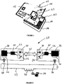
- FIG. 1 represents an exploded perspective view of a known smart card 10 with mixed contact and contactless operation.
- This smart card comprises a first electronic module 11 provided with standardized ISO 7816 contacts, and a second electronic module 12, which comprises in particular biometric sensors such as fingerprint sensors.
- the first electronic module comprises a microelectronic chip which in particular securely stores reference biometric fingerprints of the cardholder.
- the user In order to authorize a transaction with the smart card, the user must submit his biometric fingerprint to the second electronic module 12, and this fingerprint must then be transmitted securely to the first electronic module 1. It is therefore necessary to set up a communication channel between the first and second modules 11, 12.
- the known smart card 10 comprises a printed circuit 13 (or PCB for "Printed Circuit Board” in English terminology) making it possible to establish a complex circuit 14 between the two modules 11,12, performing both the power supply of the second module by the first module, and communication between the two modules.
- This printed circuit 13 must be integrated between external faces 15, 16 of the smart card, which is more complicated and more expensive to produce than simply transferring an electronic module into a cavity arranged in a monolithic card body.
- the figure 2 shows the architecture of a new type of smart card 20 with several modules according to the invention.
- the card body has not been shown, but only the functional elements which are the electronic modules and the antennas.
- the smart card 20 comprises a first module 21 or master module, a second module 22 or sensor module, an amplification antenna 23 for communication with a contactless reader 24, and a communication channel 25 between the two modules 21, 22.
- the first module 21 comprises a microelectronic chip 26 which is for example a conventional secure chip such as those commonly used in smart cards, configured to process secure information from the bearer in the context of conventional smart card applications such as banking applications, physical or logical access control, or equivalent.
- the chip 26 is connected to a clean inductor 27 which is electromagnetically coupled with a clean inductor 28 of the amplification antenna 23.
- the first module 21 further comprises a microcontroller 29 connected on the one hand to the chip 26 and on the other hand to an optical communication stage comprising an emission diode LED 30 and a reception photodiode 31.
- the smart card 20 further comprises a second electronic module 22, comprising a microelectronic chip 32, which may vary depending on the intended applications for the smart card 20. In an advantageous embodiment, it may be a chip associated with a biometric sensor (not shown) such as a fingerprint sensor.
- the chip 33 is connected to a clean inductor 33 which is electromagnetically coupled with a clean inductor 34 of the amplification antenna 23.
- module 22 further comprises a microcontroller 35 connected on the one hand to chip 32 and on the other hand to an optical communication stage comprising an emission LED diode 36 and a reception photodiode 37
- the two modules 21, 22 are arranged in the smart card so that the optical stages face each other to define an optical path 25 between the two modules 21, 22.
- the optical wave for example the light emitted by the LED 30 must be able to be picked up by the photodiode 37, and the light emitted by the LED 36 must be able to be picked up by the photodiode 31.
- the optical communication is done by any appropriate protocol, for example according to the so-called LIFI protocol, and at any suitable wavelength, for example in the visible light spectrum, but not necessarily.
- the amplification antenna 23 includes a large own main inductance 38, close to the so-called ID1 format of the smart card, making it possible to communicate with a smart card reader 24 located at a distance from the smart card.
- This arrangement makes it possible, when using the smart card, to capture biometric data from the user by means of biometric sensors associated with the chip 32, then to transmit the biometric data from the module 22 to the module 21 via the optical communication channel 25 which will process the data to authorize or not a transaction with the chip card.
- the smart card 20 can comprise, as required, a single module 22, or several modules, all connected to the main module 21 by a optical channel fully integrated into the smart card, so that the sensitive data exchanged between the modules transits inside the smart card without being able to be picked up by external devices.
- two modules 21, 22 are integrated on the same side of the smart card, by transfer and gluing in cavities provided in the card body as is well known per se.
- the amplification antenna 23 is inserted between layers of the card body, and visible only on the edge in this figure.
- the component references are those of the picture 2 .
- the module 21 comprises a drop 39 for coating the components 26, 29, 30, 31 of the module, intended to protect these components.
- the module 22 similarly comprises a coating drop 40 of the components 32, 35, 36, 37 of the module.
- the coating drops 39, 40 be made of a material transparent to the optical wave which must pass, for example visible light, at least at certain wavelengths thereof.
- the chip card further comprises a layer 41 of a material that is also optically transparent, this layer 41 being optically coupled with the coating drops 39, 40, so that an optical signal emitted by the LED of one of the modules 21, 22 can be picked up by the photodiode of the other module.
- the transparent layer 41 does not open onto the edges of the card, so that the optical signal remains confined inside the card body.
- the optical signal could be transmitted from module to module via an optical fiber.
- FIG 4 another even simpler embodiment has been shown schematically, in which the two modules are each arranged on one face of the smart card and opposite one another.
- a layer of optically transparent material 41 is unnecessary, in the measure or the coating drops 39, 40 are arranged face to face so as to allow direct optical communication between the two modules 21, 22.
- the master module 21 of the communicating portable object is a smart card module
- the slave module 22 is a fingerprint sensor module.
- the user places the smart card 20 in the electromagnetic field of a contactless reader of a user identification system. Consequently, the inductors 28, 24 of the card ( picture 2 ) are under voltage and as they are coupled to the inductors 27, 33 of the modules 21, 22, said modules are supplied with energy.
- reader 24 initiates radio frequency communication with master module 21.
- reader 24 displays a request for the user to place a finger on the fingerprint sensor. of his smart card.
- the sensor module 22 captures the fingerprint and the master module 21 asks it to communicate the captured fingerprint to it.
- the sensor module 22 transmits the user's fingerprint, via the optical channel 25 as described above.
- the master module 21 compares the fingerprint received from the fingerprint sensor 22, with a reference fingerprint of the user, previously stored securely in a memory of the master module 21.
- the reader launches a new fingerprint entry and comparison operation. If the two fingerprints match, the user is identified, and at 58 the intended transaction with the master module (physical or logical access) is authorized.
- the authentication of the user is of the "match on card” type according to the dedicated Anglo-Saxon terminology, i.e. it takes place inside of the smart card, and the user does not have to give his fingerprint to a third-party reader who could use it without his knowledge.
- the invention proposes a communicating portable object, in particular a smart card or an electronic passport, making it possible to achieve the intended goals.
- the use of optical communication between modules eliminates the need for a PCB printed circuit, which contributes to reducing the cost of manufacturing the smart card and increasing the manufacturing yield.
- the structure of the chip card according to the invention is compatible with the usual low-cost, high-yield manufacturing methods, consisting of integrating electronic modules into surface cavities of the card body. Furthermore, there is no possible interference between the radiofrequency communication between card and reader, and the optical communication between modules.
- the proposed technology makes it possible to easily integrate and communicate several modules of different types in a smart card or in an equivalent communicating device, without the need for wired connections between the modules, which means that the devices will be particularly resistant to reliability and have a long service life.
- the optical communication between modules makes the proposed solution particularly secure and difficult to intercept by a potential fraudster.
Landscapes
- Engineering & Computer Science (AREA)
- Computer Hardware Design (AREA)
- Microelectronics & Electronic Packaging (AREA)
- Physics & Mathematics (AREA)
- General Physics & Mathematics (AREA)
- Theoretical Computer Science (AREA)
- Computer Networks & Wireless Communication (AREA)
- Computer Security & Cryptography (AREA)
- General Engineering & Computer Science (AREA)
- Automation & Control Theory (AREA)
- Credit Cards Or The Like (AREA)
- Coupling Device And Connection With Printed Circuit (AREA)
Description
- L'invention concerne les objets portables sécurisés et communicants tels que notamment les cartes ou documents d'identification à puce, pourvus d'un premier module microélectronique à fonctionnement sans contact ou à fonctionnement mixte à contact et sans contact, et d'un second module ou composant électronique tel qu'un capteur biométrique destiné à communiquer avec le premier module, ainsi qu'une antenne intégrée au corps de l'objet portable pour communiquer à distance avec un lecteur radiofréquence. A titre d'exemple et de simplification de l'exposé, l'invention sera décrite dans le cadre de son application aux cartes à puce, sans pour autant limiter la portée de l'invention à d'autres objets portables ou d'autres facteurs de forme.
- Les cartes à puce à fonctionnement sans contact et réalisées au format ISO 7816-1 constituent l'exemple le plus répandu des cartes d'identification auxquelles s'applique l'invention.
- La plupart des cartes à puce sans contact ou des cartes duales à fonctionnement mixte à contact et sans contact connues comportent un corps de carte, un module électronique inséré dans une cavité du corps de carte et pourvu d'une puce microélectronique, et une antenne disposée dans le corps de carte et électriquement connectée à des plots de sortie de la puce microélectronique.
- Alternativement, il existe des cartes à puce dont l'antenne du corps de carte est en couplage inductif avec le module électronique pourvu lui-même d'une antenne.
- L'antenne du corps de carte est généralement constituée de spires réalisées à l'aide de pistes électriquement conductrices, réalisées sur un insert ou substrat flexible qui est intégré au corps de carte pendant l'assemblage de la carte.
- Afin d'obtenir des performances de communication sans contact adéquates, et en particulier une portée de fonctionnement suffisante, les spires de l'antenne doivent être de grande taille, typiquement au format dit ID1, qui correspond aux mesures de 85,60 x 53,98 mm pour le corps de carte. Ce format est communément utilisé notamment pour les cartes bancaires.
- Dans un certain nombre d'applications, il devient nécessaire d'intégrer à la carte à puce un ou plusieurs modules électroniques complémentaires par rapport au module principal, par exemple pour l'intégration de capteurs biométriques susceptibles de collecter des informations biométriques et de les transmettre au module principal à des fins d'identification biométrique de l'utilisateur de la carte à puce.
- Dans ce cas, comme par exemple dans le cas de la carte représentée en
figure 1 , les capteurs et le module sont disposés sur un substrat de type PCB et interconnectés par des pistes physiques, filaires ou en couche mince métallique. Cet arrangement présente plusieurs inconvénients. - En effet, l'interconnexion de plusieurs modules disposés sur un substrat PCB est coûteux car il nécessite des composants supplémentaires et une modification des processus de fabrication classiques des cartes à puce. Elle est en outre peu fiable dans le temps car les flexions répétées que le produit devra subir au cours de son utilisation risquent de rompre plus ou moins rapidement les interconnexions électriques entre les modules.
- On connaît aussi de par le document
EP 2 098 981 A1 un objet portable comportant une première antenne inductive et une pluralité de puces comportant chacune un circuit intégré et une seconde antenne inductive pour l'alimentation et la communication dudit circuit intégré. Certaines des puces n'ont pas vocation à communiquer avec un lecteur externe, mais uniquement avec d'autres puces de l'objet portable. Ce document prévoit donc une architecture selon laquelle les puces peuvent communiquer entre elles de manière indépendante sans utiliser l'antenne prévue pour communiquer avec l'extérieur, mais par couplage inductif entre elles. - Le document
FR 2 727 227 A1 - Le but général de l'invention est par conséquent de proposer une nouvelle structure d'objet portable communicant, notamment de carte à puce ou équivalent dénuée des inconvénients ci-dessus, et en particulier une structure permettant de faire communiquer entre eux sans connexion électrique les différents modules électroniques et capteurs intégrés dans la carte à puce ou des documents de sécurité équivalents.
- Un autre but de l'invention est de faire communiquer plusieurs modules au sein d'une même carte à puce ou équivalent, tout en utilisant un procédé de fabrication déjà existant et bien maitrisé, à savoir le report des modules électroniques dans des cavités aménagées dans le corps de carte, sans utiliser de PCB couvrant la surface de la carte.
- Selon le principe de l'invention, les différents modules sont alimentés électriquement à l'aide d'une antenne susceptible de recevoir l'énergie de l'antenne du lecteur de façon à être autonomes en énergie. En outre, pour communiquer entre eux, les différents modules électroniques sont connectés entre eux par une liaison optique qui est réalisée dans le corps de la carte.
- L'ensemble permet donc de réaliser des cartes avec des fonctionnalités complexes, de manière sécurisée, puisque l'information circule dans l'épaisseur de l'objet, notamment dans la tranche de la carte à puce, mais ne débouche pas sur l'extérieur.
- L'invention porte par conséquent sur un document d'identification à puce à fonctionnement sans contact ou à fonctionnement mixte à contact et sans contact, apte à communiquer par radiofréquence avec un lecteur externe, selon les revendications indépendantes 1 et 3.
- Selon un mode de réalisation de l'invention, ladite interface optique comporte pour chaque module une photodiode et une LED d'émission, la photodiode d'une interface optique donnée étant optiquement couplée à la LED d'émission d'une autre interface optique.
- Dans un mode de réalisation avantageux, l'objet portable communicant comporte deux modules électroniques qui sont disposés en regard l'un de l'autre de façon à présenter leurs interfaces optiques en face l'une de l'autre, et chaque module comporte une goutte d'enrobage transparente qui laisse passer l'onde optique, par exemple la lumière visible, entre les interfaces optiques des deux modules, pour au moins certaines longueurs d'onde.
- Selon un autre mode de réalisation, l'objet comporte deux modules électroniques disposés en regard l'un de l'autre de façon à présenter leurs interfaces optiques en face l'une de l'autre, et un troisième module optiquement connecté à au moins l'un des autres modules par une couche optique transparente.
- Selon un mode de réalisation avantageux de l'invention, au moins l'un des modules électroniques de l'objet comporte un capteur biométrique, par exemple un capteur d'empreintes digitales.
- De préférence, chaque module électronique comporte une inductance propre apte à récupérer l'énergie du signal radiofréquence du lecteur. Ceci permet d'alimenter électriquement le module électronique directement par le lecteur, sans nécessiter de batterie à bord de l'objet portable communicant.
- Afin d'assurer une portée de communication radiofréquence suffisante, chaque inductance propre de module est couplée électro magnétiquement à une antenne d'amplification disposée dans le corps de l'objet et assurant la liaison radiofréquence avec l'antenne du lecteur.
- D'autres caractéristiques et avantages de l'invention apparaîtront à la lecture de la description détaillée effectuée dans l'application de l'invention à une carte à puce, et des dessins annexés dans lesquels :
- la
figure 1 représente une carte à puce sans contact connue, en vue en perspective éclatée ; - la
figure 2 représente un schéma de principe d'une carte à puce selon l'invention; - la
figure 3 représente une vue en coupe transversale d'un premier mode de réalisation d'une carte à puce selon l'invention; - la
figure 4 représente une vue en coupe transversale d'un second mode de réalisation d'une carte à puce selon l'invention; - la
figure 5 représente un organigramme du procédé de mise en œuvre d'une carte à puce selon l'invention. - On se réfère à la
Figure 1 , qui représente une vue en perspective éclatée d'une carte à puce connue 10 à fonctionnement mixte à contact et sans contact. Cette carte à puce comporte un premier module électronique 11 pourvu de contacts ISO 7816 normalisés, et un second module électronique 12, qui comporte notamment des capteurs biométriques tels que des capteurs d'empreintes digitales. Le premier module électronique comporte une puce microélectronique qui en particulier stocke de façon sécurisée des empreintes biométriques de référence du porteur de la carte. Afin d'autoriser une transaction avec la carte à puce, l'utilisateur doit soumettre son empreinte biométrique au second module électronique 12, et cette empreinte doit ensuite être transmise de façon sécurisée au premier module électronique 1. Il est donc nécessaire de mettre en place un canal de communication entre les premier et second modules 11, 12. - A cet effet, la carte à puce connue 10 comporte un circuit imprimé 13 (ou PCB pour "Printed Circuit Board" en terminologie anglo-saxonne) permettant d'établir un circuit complexe 14 entre les deux modules 11,12, réalisant aussi bien l'alimentation électrique du second module par le premier module, et la communication entre les deux modules. Ce circuit imprimé 13 doit être intégré entre des faces externes 15, 16 de la carte à puce, ce qui est plus compliqué et plus coûteux à réaliser que de simplement reporter un module électronique dans une cavité aménagée dans un corps de carte monolithique.
- La
figure 2 montre l'architecture d'un nouveau type de carte à puce 20 à plusieurs modules selon l'invention. Dans ce schéma, pour simplifier, on n'a pas représenté le corps de carte, mais uniquement les éléments fonctionnels que sont les modules électroniques et les antennes. - La carte à puce 20 comporte un premier module 21 ou module maître, un second module 22 ou module capteur, une antenne d'amplification 23 pour la communication avec un lecteur sans contact 24, et un canal de communication 25 entre les deux modules 21, 22.
- Le premier module 21 comporte une puce microélectronique 26 qui est par exemple une puce sécurisée classique telle que celles couramment utilisées dans les cartes à puce, configurée pour traiter des informations sécurisées du porteur dans le cadre d'applications classiques de carte à puce telles que des applications bancaires, de contrôle d'accès physique ou logique, ou équivalent. La puce 26 est connectée à une inductance propre 27 qui est couplée électro magnétiquement avec une inductance propre 28 de l'antenne d'amplification 23.
- Le premier module 21 comporte en outre un microcontrôleur 29 connecté d'une part à la puce 26 et d'autre part à un étage de communication optique comportant une diode d'émission LED 30 et une photodiode de réception 31.
- La carte à puce 20 comporte en outre un second module électronique 22, comportant une puce microélectronique 32, qui peut varier en fonction des applications visées pour la carte à puce 20. Dans un mode de réalisation avantageux, il peut s'agir d'une puce associée à un capteur biométrique (non représenté) tel qu'un capteur d'empreintes digitales. La puce 33 est connectée à une inductance propre 33 qui est couplée électro magnétiquement avec une inductance propre 34 de l'antenne d'amplification 23.
- De façon similaire au module 21, le module 22 comporte en outre un microcontrôleur 35 connecté d'une part à la puce 32 et d'autre part à un étage de communication optique comportant une diode LED d'émission 36 et une photodiode de réception 37. Bien entendu les deux modules 21, 22 sont disposés dans la carte à puce de manière que les étages optiques soient en regard pour définir un chemin optique 25 entre les deux modules 21, 22. En particulier, l'onde optique, par exemple la lumière émise par la LED 30 doit pouvoir être captée par la photodiode 37, et la lumière émise par la LED 36 doit pouvoir être captée par la photodiode 31. La communication optique se fait par tout protocole approprié, par exemple selon le protocole dit LIFI, et à toute longueur d'onde appropriée, par exemple dans le spectre de la lumière visible, mais pas nécessairement.
- L'antenne d'amplification 23 comporte une inductance propre principale 38 de grande taille, proche du format dit ID1 de la carte à puce, permettant de communiquer avec un lecteur de carte à puce 24 situé à distance de la carte à puce.
- Cet agencement permet, lors de l'utilisation de la carte à puce, de capter des données biométriques de l'utilisateur au moyen de capteurs biométriques associés à la puce 32, puis de transmettre les données biométriques du module 22 vers le module 21 via le canal de communication optique 25 qui traitera les données pour autoriser ou non une transaction avec la carte à puce.
- Il est à noter que la carte à puce 20 peut comporter selon les besoins un seul module 22, ou plusieurs modules, tous connectés au module principal 21 par un canal optique totalement intégré à la carte à puce, de sorte que les données sensibles échangées entre les modules transitent à l'intérieur de la carte à puce sans pouvoir être captées par des dispositifs externes.
- On se réfère maintenant aux
figures 3 et 4 pour décrire des modalités pratiques de réalisation du canal de communication optique entre les différents modules de la carte à puce. Les figures sont schématiques et l'épaisseur de la carte à puce est exagérée pour plus de clarté. - En
figure 3 , deux modules 21, 22 sont intégrés du même côté de la carte à puce, par report et collage dans des cavités aménagées dans le corps de carte comme bien connu en soi. L'antenne d'amplification 23 est insérée entre des couches du corps de carte, et visible uniquement sur la tranche dans cette figure. Les références des composants sont celles de lafigure 2 . Le module 21 comporte une goutte 39 d'enrobage des composants 26, 29, 30, 31 du module, destinée à protéger ces composants. Le module 22 comporte de façon similaire une goutte d'enrobage 40 des composants 32, 35, 36, 37 du module. - Il est important que les gouttes d'enrobage 39, 40 soient réalisées en un matériau transparent à l'onde optique qui doit passer, par exemple la lumière visible, du moins à certaines longueurs d'ondes de celle-ci. Dans le mode de réalisation représenté, la carte à puce comporte en outre une couche 41 d'un matériau également optiquement transparent, cette couche 41 étant couplée optiquement avec les gouttes d'enrobage 39, 40, de façon qu'un signal optique émis par la LED de l'un des modules 21, 22 puisse être capté par la photodiode de l'autre module. De préférence, la couche transparente 41 ne débouche pas sur les bords de carte, de façon que le signal optique reste confiné à l'intérieur du corps de carte. A la place d'une simple couche optiquement transparente, le signal optique pourrait être transmis de module à module par l'intermédiaire d'une fibre optique.
- En
figure 4 on a représenté de façon schématique un autre mode de réalisation encore plus simple, dans lequel les deux modules sont disposés chacun sur une face de la carte à puce et en regard l'un de l'autre. Dans ce mode de réalisation, une couche de matériau optiquement transparent 41 est inutile, dans la mesure ou les gouttes d'enrobage 39, 40 sont disposées en face à face de manière à permettre une communication optique directe entre les deux modules 21, 22. - Bien entendu, dans le cas d'une carte à puce à trois modules ou plus, on pourra combiner les modes de réalisation des
figures 3 et 4 , certains modules étant disposés en regard et d'autres étant optiquement connectés par une couche transparente 41. - On décrit maintenant en référence à la
figure 5 , un exemple de cas d'usage de l'invention, dans lequel le module maitre 21 de l'objet portable communicant est un module de carte à puce, et le module esclave 22 est un module capteur d'empreintes digitales. - En 50, l'utilisateur place la carte à puce 20 dans le champ électromagnétique d'un lecteur sans contact d'un système d'identification de l'utilisateur. En conséquence, les inductances 28, 24 de la carte (
figure 2 ) sont sous tension et comme elles sont couplées aux inductances 27, 33 des modules 21, 22, lesdits modules sont alimentés en énergie. - En 52, le lecteur 24 initie la communication radiofréquence avec le module maître 21. Lorsque la communication entre la carte 20 et le lecteur 24 est établie, le lecteur 24 affiche pour l'utilisateur une demande de placer un doigt sur le capteur d'empreintes de sa carte à puce. En 54, le module capteur 22 saisit l'empreinte digitale et le module maître 21 lui demande de lui communiquer l'empreinte digitale saisie. En 55, le module capteur 22 transmet l'empreinte digitale de l'utilisateur, via le canal optique 25 comme décrit plus haut. En 56, le module maître 21 compare l'empreinte digitale reçue du capteur d'empreinte 22, avec une empreinte de référence de l'utilisateur, préalablement stockée de manière sécurisée dans une mémoire du module maître 21. En 57, si les deux empreintes diffèrent, le lecteur lance une nouvelle opération de saisie et comparaison d'empreinte. Si les deux empreintes correspondent, l'utilisateur est identifié, et en 58 la transaction visée avec le module maître (accès physique ou logique) est autorisée.
- Dans ce cas l'authentification de l'utilisateur est de type "match on card" selon la terminologie anglo-saxonne dédiée, c'est à dire qu'elle se passe à l'intérieur de la carte à puce, et l'utilisateur n'a pas à donner son empreinte à un lecteur tiers qui pourrait l'utiliser à son insu.
- En définitive, l'invention propose un objet portable communicant, notamment une carte à puce ou un passeport électronique, permettant d'atteindre les buts visés. En particulier, l'utilisation d'une communication optique entre modules élimine d'avoir recours à un circuit imprimé PCB, ce qui contribue à diminuer le coût de fabrication de la carte à puce et à augmenter le rendement de fabrication. En outre, la structure de la carte à puce selon l'invention est compatible avec les procédés de fabrication usuels à faible coût et haut rendement, consistant à intégrer des modules électroniques dans des cavités superficielles du corps de carte. Par ailleurs, il n'y a pas d'interférence possible entre la communication radiofréquence entre carte et lecteur, et la communication optique entre modules. La technologie proposée permet d'intégrer et de faire communiquer aisément plusieurs modules de types différents dans une carte à puce ou dans un dispositif communicant équivalent, sans nécessité de connexions filaires entre les modules, ce qui signifie que les dispositifs seront particulièrement résistants aux tests de fiabilité et présenteront une longue durée de vie. La communication optique entre modules fait que la solution proposée est particulièrement sûre et difficile à intercepter par un fraudeur potentiel.
Claims (9)
- - Document d'identification à puce (20) à fonctionnement sans contact ou à fonctionnement mixte à contact et sans contact, apte à communiquer par radiofréquence avec un lecteur externe (24), et comportant un corps dans lequel est intégrée au moins une antenne (23), un premier module électronique (21) pourvu d'une puce microélectronique (26), au moins un second module électronique (22) agencé pour pouvoir communiquer avec ledit premier module électronique (21), et un chemin optique (25) aménagé entre ledit premier module électronique (21) et ledit au moins un second module électronique (22), lesdits modules électroniques (21,22) étant physiquement séparés et répartis dans le corps du document d'identification (20) et comportant chacun une interface optique (30, 31 ; 36, 37), caractérisé en ce que chacun des modules électroniques (21, 22) comporte une goutte de résine d'enrobage (39, 40) configurée de manière à protéger lesdites interfaces optiques et réalisée en une matière optiquement transparente à au moins certaines longueurs d'onde de la lumière, et lesdites gouttes d'enrobage (39, 40) étant optiquement couplées à travers ledit chemin optique (25).
- - Document d'identification selon la revendication 1, caractérisé en ce que ledit chemin optique (25) est constitué par une couche (41) en matériau optiquement transparent ou par une fibre optique.
- - Document d'identification à puce (20) à fonctionnement sans contact ou à fonctionnement mixte à contact et sans contact, apte à communiquer par radiofréquence avec un lecteur externe (24), et comportant un corps dans lequel est intégrée au moins une antenne (23), un premier module électronique (21) pourvu d'une puce microélectronique (26) et un second module électronique (22) disposé en regard du premier module électronique (21), lesdits modules électroniques (21,22) comportant chacun une interface optique (30, 31; 36, 37),
caractérisé en ce que chacun des modules électroniques (21, 22) comporte une goutte de résine d'enrobage (39, 40) configurée de manière à protéger lesdites interfaces optiques et réalisée en une matière optiquement transparente à au moins certaines longueurs d'onde de la lumière, et en ce que les gouttes d'enrobage (39, 40) sont disposées en face à face de manière à permettre une communication optique directe entre les deux modules (21, 22). - - Document d'identification à puce (20) selon l'une quelconque des revendications précédentes, caractérisé en ce que ladite interface optique (30, 31 ; 36, 37) comporte pour chaque module (20, 21) une photodiode (30;36) et une LED d'émission (31;37), la photodiode d'une interface optique donnée étant optiquement couplée à la LED d'émission d'une autre interface optique.
- - Document d'identification à puce (20) selon l'une des revendications 3 ou 4, caractérisé en ce qu'il comporte deux modules électroniques en regard l'un de l'autre de façon à présenter leurs interfaces optiques en face l'une de l'autre, et un troisième module optiquement connecté à au moins l'un des autres modules par une couche optique transparente (41).
- - Document d'identification à puce (20) selon l'une quelconque des revendications précédentes, caractérisé en ce qu'au moins l'un des modules électroniques (20, 21) comporte un capteur biométrique.
- - Document d'identification à puce (20) selon l'une quelconque des revendications précédentes, caractérisé en ce que chaque module électronique (20, 21) comporte une inductance propre (27, 33) apte à récupérer l'énergie du signal radiofréquence du lecteur (24) pour alimenter électriquement le module électronique (20,21).
- - Document d'identification à puce (20) selon la revendication 7, caractérisé en ce que chaque inductance propre (27, 33) de module est couplée électro magnétiquement à une antenne d'amplification (23) disposée dans le corps de l'objet (20) et assurant la liaison radiofréquence avec l'antenne du lecteur (24).
- - Document d'identification à puce (20) selon l'une quelconque des revendications précédentes, caractérisé en ce qu'il se présente sous la forme d'une carte à puce au format ISO 7816-1, ou au format d'un passeport électronique.
Applications Claiming Priority (2)
| Application Number | Priority Date | Filing Date | Title |
|---|---|---|---|
| FR1800173A FR3078422B1 (fr) | 2018-02-28 | 2018-02-28 | Carte a puce sans contact a modules electroniques multiples communicants |
| PCT/FR2019/000025 WO2019166706A1 (fr) | 2018-02-28 | 2019-02-26 | Carte à puce sans contact à modules électroniques multiples communicants |
Publications (2)
| Publication Number | Publication Date |
|---|---|
| EP3759651A1 EP3759651A1 (fr) | 2021-01-06 |
| EP3759651B1 true EP3759651B1 (fr) | 2022-10-19 |
Family
ID=63490496
Family Applications (1)
| Application Number | Title | Priority Date | Filing Date |
|---|---|---|---|
| EP19711955.5A Active EP3759651B1 (fr) | 2018-02-28 | 2019-02-26 | Carte à puce sans contact à modules électroniques multiples communicants |
Country Status (4)
| Country | Link |
|---|---|
| EP (1) | EP3759651B1 (fr) |
| ES (1) | ES2936247T3 (fr) |
| FR (1) | FR3078422B1 (fr) |
| WO (1) | WO2019166706A1 (fr) |
Families Citing this family (2)
| Publication number | Priority date | Publication date | Assignee | Title |
|---|---|---|---|---|
| DE102019128474A1 (de) * | 2019-10-22 | 2021-04-22 | Infineon Technologies Ag | Dual-Interface-Chipkarte und Verfahren zum Bilden einer Dual-Interface-Chipkarte |
| FR3144685B1 (fr) * | 2022-12-29 | 2025-08-01 | Smart Packaging Solutions | Carte à puce sans contact à modules électroniques multiples communicants |
Family Cites Families (5)
| Publication number | Priority date | Publication date | Assignee | Title |
|---|---|---|---|---|
| JPS629487A (ja) * | 1985-07-05 | 1987-01-17 | Matsushita Electric Ind Co Ltd | Icカ−ド |
| FR2727227B1 (fr) * | 1994-11-17 | 1996-12-20 | Schlumberger Ind Sa | Dispositif de securite actif a memoire electronique |
| EP1387323A1 (fr) * | 2002-07-30 | 2004-02-04 | Omega Electronics S.A. | Authentification par mesure biométrique du porteur d'un dispositif d'identification et/ou d'accès portable d'un système d'identification et/ou d'accès électronique |
| FR2883653B1 (fr) * | 2005-03-22 | 2007-05-25 | Gemplus Sa | Module electronique et carte a puce avec indicateur lumineux |
| FR2928475B1 (fr) * | 2008-03-05 | 2010-05-07 | Commissariat Energie Atomique | Dispositif de communication sans contact. |
-
2018
- 2018-02-28 FR FR1800173A patent/FR3078422B1/fr active Active
-
2019
- 2019-02-26 WO PCT/FR2019/000025 patent/WO2019166706A1/fr not_active Ceased
- 2019-02-26 EP EP19711955.5A patent/EP3759651B1/fr active Active
- 2019-02-26 ES ES19711955T patent/ES2936247T3/es active Active
Also Published As
| Publication number | Publication date |
|---|---|
| EP3759651A1 (fr) | 2021-01-06 |
| WO2019166706A1 (fr) | 2019-09-06 |
| FR3078422B1 (fr) | 2021-05-07 |
| FR3078422A1 (fr) | 2019-08-30 |
| ES2936247T3 (es) | 2023-03-15 |
Similar Documents
| Publication | Publication Date | Title |
|---|---|---|
| EP2507747B1 (fr) | Activation et indication d'un champ rf sur un dispositif comprenant une puce | |
| EP2220597B1 (fr) | Systeme a double circuit integre et utilisation du systeme a la mise en oeuvre d'application a distance | |
| FR2942365A1 (fr) | Dispositif de communication incluant une batterie et un module de communication a champ proche | |
| FR3063555A1 (fr) | Carte a puce et procede de fabrication d’une carte a puce | |
| EP2065857A2 (fr) | Carte à microprocesseur, téléphone comprenant une telle carte et procédé d'exécution d'une commande dans une telle carte | |
| FR3069081A1 (fr) | Carte electronique comprenant un capteur d'empreinte et procede de fabrication d'une telle carte | |
| WO2010060986A1 (fr) | Objet portable intelligent comportant des données de personnalisation graphique | |
| WO2006100206A1 (fr) | Module electronique et carte a puce avec indicateur lumineux | |
| FR2637749A1 (fr) | Dispositif pour la transmission a distance d'informations d'identification et/ou de valeur | |
| EP3759651A1 (fr) | Carte à puce sans contact à modules électroniques multiples communicants | |
| EP2936379B1 (fr) | Détection d'un dispositif transactionnel | |
| EP4416636B1 (fr) | Carte à puce avec capteur biométrique | |
| EP3794507B1 (fr) | Passeport electronique securise contre les lectures non autorisees | |
| WO2023126590A1 (fr) | Dispositif biométrique de transaction par carte à puce | |
| WO2024141722A1 (fr) | Carte à puce sans contact à modules électroniques multiples communicants | |
| EP1048003A1 (fr) | Systeme pour la communication securisee sans contact entre un terminal et un objet portatif tel qu'une carte a puce | |
| FR2770315A1 (fr) | Systeme pour la communication securisee sans contact entre un terminal et un objet portatif tel qu'une carte a puce | |
| FR3142579A1 (fr) | Module électronique à puces multiples pour carte à puce sans contact | |
| FR3142580A1 (fr) | Document électronique et procédé de commande d’une transaction mis en œuvre par un tel document | |
| EP3182338A1 (fr) | Procede de fabrication d'un dispositif comprenant un module electronique radiofrequence et un indicateur | |
| FR3058544A1 (fr) | Module et carte a puce a mesure photo plethysmographique | |
| WO2021014080A1 (fr) | Module de document électronique comportant une puce et une interface de contact avec une antenne connectée à un port i/o de la puce, document électronique comportant un tel module et procédé de vérification d'une connexion entre le module et une antenne correspondant | |
| FR3003672B1 (fr) | Carte a puce a double interface de communication avec carte micro sd incorporee | |
| EP2202677A1 (fr) | Carte à microcircuit et terminal mobile comprenant une telle carte | |
| FR2949589A1 (fr) | Dispositif electronique comprenant une carte a microcircuit |
Legal Events
| Date | Code | Title | Description |
|---|---|---|---|
| STAA | Information on the status of an ep patent application or granted ep patent |
Free format text: STATUS: UNKNOWN |
|
| STAA | Information on the status of an ep patent application or granted ep patent |
Free format text: STATUS: THE INTERNATIONAL PUBLICATION HAS BEEN MADE |
|
| PUAI | Public reference made under article 153(3) epc to a published international application that has entered the european phase |
Free format text: ORIGINAL CODE: 0009012 |
|
| STAA | Information on the status of an ep patent application or granted ep patent |
Free format text: STATUS: REQUEST FOR EXAMINATION WAS MADE |
|
| 17P | Request for examination filed |
Effective date: 20201023 |
|
| AK | Designated contracting states |
Kind code of ref document: A1 Designated state(s): AL AT BE BG CH CY CZ DE DK EE ES FI FR GB GR HR HU IE IS IT LI LT LU LV MC MK MT NL NO PL PT RO RS SE SI SK SM TR |
|
| AX | Request for extension of the european patent |
Extension state: BA ME |
|
| DAV | Request for validation of the european patent (deleted) | ||
| DAX | Request for extension of the european patent (deleted) | ||
| STAA | Information on the status of an ep patent application or granted ep patent |
Free format text: STATUS: EXAMINATION IS IN PROGRESS |
|
| 17Q | First examination report despatched |
Effective date: 20210923 |
|
| GRAP | Despatch of communication of intention to grant a patent |
Free format text: ORIGINAL CODE: EPIDOSNIGR1 |
|
| STAA | Information on the status of an ep patent application or granted ep patent |
Free format text: STATUS: GRANT OF PATENT IS INTENDED |
|
| INTG | Intention to grant announced |
Effective date: 20220728 |
|
| GRAS | Grant fee paid |
Free format text: ORIGINAL CODE: EPIDOSNIGR3 |
|
| GRAA | (expected) grant |
Free format text: ORIGINAL CODE: 0009210 |
|
| STAA | Information on the status of an ep patent application or granted ep patent |
Free format text: STATUS: THE PATENT HAS BEEN GRANTED |
|
| AK | Designated contracting states |
Kind code of ref document: B1 Designated state(s): AL AT BE BG CH CY CZ DE DK EE ES FI FR GB GR HR HU IE IS IT LI LT LU LV MC MK MT NL NO PL PT RO RS SE SI SK SM TR |
|
| REG | Reference to a national code |
Ref country code: GB Ref legal event code: FG4D Free format text: NOT ENGLISH |
|
| REG | Reference to a national code |
Ref country code: CH Ref legal event code: EP |
|
| REG | Reference to a national code |
Ref country code: DE Ref legal event code: R096 Ref document number: 602019020799 Country of ref document: DE |
|
| REG | Reference to a national code |
Ref country code: IE Ref legal event code: FG4D Free format text: LANGUAGE OF EP DOCUMENT: FRENCH |
|
| REG | Reference to a national code |
Ref country code: AT Ref legal event code: REF Ref document number: 1526031 Country of ref document: AT Kind code of ref document: T Effective date: 20221115 |
|
| REG | Reference to a national code |
Ref country code: SE Ref legal event code: TRGR |
|
| REG | Reference to a national code |
Ref country code: LT Ref legal event code: MG9D |
|
| REG | Reference to a national code |
Ref country code: NL Ref legal event code: MP Effective date: 20221019 |
|
| REG | Reference to a national code |
Ref country code: AT Ref legal event code: MK05 Ref document number: 1526031 Country of ref document: AT Kind code of ref document: T Effective date: 20221019 Ref country code: ES Ref legal event code: FG2A Ref document number: 2936247 Country of ref document: ES Kind code of ref document: T3 Effective date: 20230315 |
|
| PG25 | Lapsed in a contracting state [announced via postgrant information from national office to epo] |
Ref country code: NL Free format text: LAPSE BECAUSE OF FAILURE TO SUBMIT A TRANSLATION OF THE DESCRIPTION OR TO PAY THE FEE WITHIN THE PRESCRIBED TIME-LIMIT Effective date: 20221019 |
|
| PG25 | Lapsed in a contracting state [announced via postgrant information from national office to epo] |
Ref country code: PT Free format text: LAPSE BECAUSE OF FAILURE TO SUBMIT A TRANSLATION OF THE DESCRIPTION OR TO PAY THE FEE WITHIN THE PRESCRIBED TIME-LIMIT Effective date: 20230220 Ref country code: NO Free format text: LAPSE BECAUSE OF FAILURE TO SUBMIT A TRANSLATION OF THE DESCRIPTION OR TO PAY THE FEE WITHIN THE PRESCRIBED TIME-LIMIT Effective date: 20230119 Ref country code: LT Free format text: LAPSE BECAUSE OF FAILURE TO SUBMIT A TRANSLATION OF THE DESCRIPTION OR TO PAY THE FEE WITHIN THE PRESCRIBED TIME-LIMIT Effective date: 20221019 Ref country code: FI Free format text: LAPSE BECAUSE OF FAILURE TO SUBMIT A TRANSLATION OF THE DESCRIPTION OR TO PAY THE FEE WITHIN THE PRESCRIBED TIME-LIMIT Effective date: 20221019 Ref country code: AT Free format text: LAPSE BECAUSE OF FAILURE TO SUBMIT A TRANSLATION OF THE DESCRIPTION OR TO PAY THE FEE WITHIN THE PRESCRIBED TIME-LIMIT Effective date: 20221019 |
|
| PG25 | Lapsed in a contracting state [announced via postgrant information from national office to epo] |
Ref country code: RS Free format text: LAPSE BECAUSE OF FAILURE TO SUBMIT A TRANSLATION OF THE DESCRIPTION OR TO PAY THE FEE WITHIN THE PRESCRIBED TIME-LIMIT Effective date: 20221019 Ref country code: PL Free format text: LAPSE BECAUSE OF FAILURE TO SUBMIT A TRANSLATION OF THE DESCRIPTION OR TO PAY THE FEE WITHIN THE PRESCRIBED TIME-LIMIT Effective date: 20221019 Ref country code: LV Free format text: LAPSE BECAUSE OF FAILURE TO SUBMIT A TRANSLATION OF THE DESCRIPTION OR TO PAY THE FEE WITHIN THE PRESCRIBED TIME-LIMIT Effective date: 20221019 Ref country code: IS Free format text: LAPSE BECAUSE OF FAILURE TO SUBMIT A TRANSLATION OF THE DESCRIPTION OR TO PAY THE FEE WITHIN THE PRESCRIBED TIME-LIMIT Effective date: 20230219 Ref country code: HR Free format text: LAPSE BECAUSE OF FAILURE TO SUBMIT A TRANSLATION OF THE DESCRIPTION OR TO PAY THE FEE WITHIN THE PRESCRIBED TIME-LIMIT Effective date: 20221019 Ref country code: GR Free format text: LAPSE BECAUSE OF FAILURE TO SUBMIT A TRANSLATION OF THE DESCRIPTION OR TO PAY THE FEE WITHIN THE PRESCRIBED TIME-LIMIT Effective date: 20230120 |
|
| REG | Reference to a national code |
Ref country code: DE Ref legal event code: R097 Ref document number: 602019020799 Country of ref document: DE |
|
| PG25 | Lapsed in a contracting state [announced via postgrant information from national office to epo] |
Ref country code: SM Free format text: LAPSE BECAUSE OF FAILURE TO SUBMIT A TRANSLATION OF THE DESCRIPTION OR TO PAY THE FEE WITHIN THE PRESCRIBED TIME-LIMIT Effective date: 20221019 Ref country code: RO Free format text: LAPSE BECAUSE OF FAILURE TO SUBMIT A TRANSLATION OF THE DESCRIPTION OR TO PAY THE FEE WITHIN THE PRESCRIBED TIME-LIMIT Effective date: 20221019 Ref country code: EE Free format text: LAPSE BECAUSE OF FAILURE TO SUBMIT A TRANSLATION OF THE DESCRIPTION OR TO PAY THE FEE WITHIN THE PRESCRIBED TIME-LIMIT Effective date: 20221019 Ref country code: DK Free format text: LAPSE BECAUSE OF FAILURE TO SUBMIT A TRANSLATION OF THE DESCRIPTION OR TO PAY THE FEE WITHIN THE PRESCRIBED TIME-LIMIT Effective date: 20221019 Ref country code: CZ Free format text: LAPSE BECAUSE OF FAILURE TO SUBMIT A TRANSLATION OF THE DESCRIPTION OR TO PAY THE FEE WITHIN THE PRESCRIBED TIME-LIMIT Effective date: 20221019 |
|
| PLBE | No opposition filed within time limit |
Free format text: ORIGINAL CODE: 0009261 |
|
| STAA | Information on the status of an ep patent application or granted ep patent |
Free format text: STATUS: NO OPPOSITION FILED WITHIN TIME LIMIT |
|
| PG25 | Lapsed in a contracting state [announced via postgrant information from national office to epo] |
Ref country code: SK Free format text: LAPSE BECAUSE OF FAILURE TO SUBMIT A TRANSLATION OF THE DESCRIPTION OR TO PAY THE FEE WITHIN THE PRESCRIBED TIME-LIMIT Effective date: 20221019 Ref country code: AL Free format text: LAPSE BECAUSE OF FAILURE TO SUBMIT A TRANSLATION OF THE DESCRIPTION OR TO PAY THE FEE WITHIN THE PRESCRIBED TIME-LIMIT Effective date: 20221019 |
|
| 26N | No opposition filed |
Effective date: 20230720 |
|
| PG25 | Lapsed in a contracting state [announced via postgrant information from national office to epo] |
Ref country code: MC Free format text: LAPSE BECAUSE OF FAILURE TO SUBMIT A TRANSLATION OF THE DESCRIPTION OR TO PAY THE FEE WITHIN THE PRESCRIBED TIME-LIMIT Effective date: 20221019 |
|
| REG | Reference to a national code |
Ref country code: CH Ref legal event code: PL |
|
| REG | Reference to a national code |
Ref country code: BE Ref legal event code: MM Effective date: 20230228 |
|
| PG25 | Lapsed in a contracting state [announced via postgrant information from national office to epo] |
Ref country code: LU Free format text: LAPSE BECAUSE OF NON-PAYMENT OF DUE FEES Effective date: 20230226 Ref country code: LI Free format text: LAPSE BECAUSE OF NON-PAYMENT OF DUE FEES Effective date: 20230228 Ref country code: CH Free format text: LAPSE BECAUSE OF NON-PAYMENT OF DUE FEES Effective date: 20230228 |
|
| PG25 | Lapsed in a contracting state [announced via postgrant information from national office to epo] |
Ref country code: SI Free format text: LAPSE BECAUSE OF FAILURE TO SUBMIT A TRANSLATION OF THE DESCRIPTION OR TO PAY THE FEE WITHIN THE PRESCRIBED TIME-LIMIT Effective date: 20221019 |
|
| REG | Reference to a national code |
Ref country code: IE Ref legal event code: MM4A |
|
| PG25 | Lapsed in a contracting state [announced via postgrant information from national office to epo] |
Ref country code: IE Free format text: LAPSE BECAUSE OF NON-PAYMENT OF DUE FEES Effective date: 20230226 |
|
| PG25 | Lapsed in a contracting state [announced via postgrant information from national office to epo] |
Ref country code: BE Free format text: LAPSE BECAUSE OF NON-PAYMENT OF DUE FEES Effective date: 20230228 |
|
| PG25 | Lapsed in a contracting state [announced via postgrant information from national office to epo] |
Ref country code: IT Free format text: LAPSE BECAUSE OF FAILURE TO SUBMIT A TRANSLATION OF THE DESCRIPTION OR TO PAY THE FEE WITHIN THE PRESCRIBED TIME-LIMIT Effective date: 20221019 |
|
| PG25 | Lapsed in a contracting state [announced via postgrant information from national office to epo] |
Ref country code: BG Free format text: LAPSE BECAUSE OF FAILURE TO SUBMIT A TRANSLATION OF THE DESCRIPTION OR TO PAY THE FEE WITHIN THE PRESCRIBED TIME-LIMIT Effective date: 20221019 |
|
| PG25 | Lapsed in a contracting state [announced via postgrant information from national office to epo] |
Ref country code: BG Free format text: LAPSE BECAUSE OF FAILURE TO SUBMIT A TRANSLATION OF THE DESCRIPTION OR TO PAY THE FEE WITHIN THE PRESCRIBED TIME-LIMIT Effective date: 20221019 |
|
| PG25 | Lapsed in a contracting state [announced via postgrant information from national office to epo] |
Ref country code: CY Free format text: LAPSE BECAUSE OF FAILURE TO SUBMIT A TRANSLATION OF THE DESCRIPTION OR TO PAY THE FEE WITHIN THE PRESCRIBED TIME-LIMIT; INVALID AB INITIO Effective date: 20190226 |
|
| PG25 | Lapsed in a contracting state [announced via postgrant information from national office to epo] |
Ref country code: HU Free format text: LAPSE BECAUSE OF FAILURE TO SUBMIT A TRANSLATION OF THE DESCRIPTION OR TO PAY THE FEE WITHIN THE PRESCRIBED TIME-LIMIT; INVALID AB INITIO Effective date: 20190226 |
|
| PGFP | Annual fee paid to national office [announced via postgrant information from national office to epo] |
Ref country code: SE Payment date: 20260121 Year of fee payment: 8 |
|
| PGFP | Annual fee paid to national office [announced via postgrant information from national office to epo] |
Ref country code: GB Payment date: 20260122 Year of fee payment: 8 |
|
| PGFP | Annual fee paid to national office [announced via postgrant information from national office to epo] |
Ref country code: ES Payment date: 20260302 Year of fee payment: 8 |
|
| PGFP | Annual fee paid to national office [announced via postgrant information from national office to epo] |
Ref country code: DE Payment date: 20260121 Year of fee payment: 8 |
|
| PGFP | Annual fee paid to national office [announced via postgrant information from national office to epo] |
Ref country code: FR Payment date: 20260121 Year of fee payment: 8 |
|
| PGFP | Annual fee paid to national office [announced via postgrant information from national office to epo] |
Ref country code: TR Payment date: 20260127 Year of fee payment: 8 |