EP3758181B1 - Bidirectional high-voltage cold-cathode field-emission vacuumelectron tube - Google Patents
Bidirectional high-voltage cold-cathode field-emission vacuumelectron tube Download PDFInfo
- Publication number
- EP3758181B1 EP3758181B1 EP20162042.4A EP20162042A EP3758181B1 EP 3758181 B1 EP3758181 B1 EP 3758181B1 EP 20162042 A EP20162042 A EP 20162042A EP 3758181 B1 EP3758181 B1 EP 3758181B1
- Authority
- EP
- European Patent Office
- Prior art keywords
- current
- grid
- voltage
- tube
- electron tube
- Prior art date
- Legal status (The legal status is an assumption and is not a legal conclusion. Google has not performed a legal analysis and makes no representation as to the accuracy of the status listed.)
- Active
Links
Images


Classifications
-
- H—ELECTRICITY
- H02—GENERATION; CONVERSION OR DISTRIBUTION OF ELECTRIC POWER
- H02H—EMERGENCY PROTECTIVE CIRCUIT ARRANGEMENTS
- H02H9/00—Emergency protective circuit arrangements for limiting excess current or voltage without disconnection
-
- H—ELECTRICITY
- H01—ELECTRIC ELEMENTS
- H01H—ELECTRIC SWITCHES; RELAYS; SELECTORS; EMERGENCY PROTECTIVE DEVICES
- H01H83/00—Protective switches, e.g. circuit-breaking switches, or protective relays operated by abnormal electrical conditions otherwise than solely by excess current
- H01H83/10—Protective switches, e.g. circuit-breaking switches, or protective relays operated by abnormal electrical conditions otherwise than solely by excess current operated by excess voltage, e.g. for lightning protection
-
- H—ELECTRICITY
- H01—ELECTRIC ELEMENTS
- H01J—ELECTRIC DISCHARGE TUBES OR DISCHARGE LAMPS
- H01J21/00—Vacuum tubes
- H01J21/02—Tubes with a single discharge path
- H01J21/06—Tubes with a single discharge path having electrostatic control means only
- H01J21/10—Tubes with a single discharge path having electrostatic control means only with one or more immovable internal control electrodes, e.g. triode, pentode, octode
-
- H—ELECTRICITY
- H02—GENERATION; CONVERSION OR DISTRIBUTION OF ELECTRIC POWER
- H02G—INSTALLATION OF ELECTRIC CABLES OR LINES, OR OF COMBINED OPTICAL AND ELECTRIC CABLES OR LINES
- H02G13/00—Installations of lightning conductors; Fastening thereof to supporting structure
-
- H—ELECTRICITY
- H02—GENERATION; CONVERSION OR DISTRIBUTION OF ELECTRIC POWER
- H02G—INSTALLATION OF ELECTRIC CABLES OR LINES, OR OF COMBINED OPTICAL AND ELECTRIC CABLES OR LINES
- H02G7/00—Overhead installations of electric lines or cables
- H02G7/22—Arrangements of earthing wires suspended between mastheads
-
- H—ELECTRICITY
- H02—GENERATION; CONVERSION OR DISTRIBUTION OF ELECTRIC POWER
- H02H—EMERGENCY PROTECTIVE CIRCUIT ARRANGEMENTS
- H02H5/00—Emergency protective circuit arrangements for automatic disconnection directly responsive to an undesired change from normal non-electric working conditions with or without subsequent reconnection
- H02H5/005—Emergency protective circuit arrangements for automatic disconnection directly responsive to an undesired change from normal non-electric working conditions with or without subsequent reconnection responsive to ionising radiation; Nuclear-radiation circumvention circuits
Definitions
- the present invention relates to a method and apparatus for preventing extraordinary electromagnetic pulses (EEMP) arising, for instance, from a nuclear explosion or solar storm, from reaching and rendering inoperative electrical components of an electrical power generation and distribution system.
- an extraordinary electromagnetic pulse EEMP
- NEMP nuclear explosions
- NNEMP non-nuclear electromagnetic pulses
- GIC geomagnetically-induced current
- a further aspect of the invention relates to a high speed current shunt which may be used for detection of GIC pulses.
- Commission Report further discusses the threat of attack to electrical power systems by an electromagnetic pulse arising from a nuclear explosion, and also refers to the naturally occurring threats to electrical power systems from geomagnetic storms. Commission Report at page18.
- electrical power systems connotes systems for generating electrical power, transmitting that power over short to long distances and distributing that power to end users.
- an EMP event can render various components of an electrical power system inoperative.
- Two such electrical components electrical generators for producing electricity and electrical transformers for stepping up or stepping down voltage levels as required for power transmission or distribution, are obviously vital. If generators or transformers cease to operate, the power system fails and society as we know it ends. Both components require a long lead time to build (e.g., 3-5 years for transformers and up to 10 years for generators) if the demand from them is normal; that is, if failures occur after expected product lifetimes. However, if the demand for generators and transformers surge due to their premature failure resulting from an EMP event, the lead time to build them increases even further and likely dramatically.
- the various forms of EMP include an unwanted transient electromagnetic pulse arising from nuclear electromagnetic pulse events (NEMP), non-nuclear electromagnetic pulse (NNEMP) events creating a pulse with a rise time of less than 500 picoseconds and a field strength (e.g., in excess of 20 volts per meter) sufficient to reach and render inoperative components of an electrical power supply system as defined above, or geomagnetically-induced currents (GIC) arising from coronal mass ejections of solar storms or other EMP events.
- NEMP nuclear electromagnetic pulse events
- NNEMP non-nuclear electromagnetic pulse
- GIC geomagnetically-induced currents
- One form of the invention provides a method and apparatus for preventing an extraordinary electromagnetic pulse from reaching and rendering inoperative an electrical component of an electrical power system, wherein the component is located in a conductive path of the system that receives the pulse.
- the method and apparatus comprises the steps or means for detecting the presence of the pulse in the conductive path prior to the pulse reaching and rendering inoperative the electrical component.
- the pulse is diverted around the electrical component with a low inductance, high current capacity circuit relative to the electrical component before the pulse can reach and render the electrical component inoperative.
- the foregoing method and apparatus prevents various forms of EEMP from reaching and rendering inoperative components of a power supply system.
- Another aspect of the invention provides a high-speed current shunt comprising a flat conductive metal strap having a defined current-measuring region, a tapered parallel-plate transmission-line matching transformer attached to the current-measuring region and an output via a coaxial cable.
- the foregoing current shunt beneficially provides a direct technique for measurement of high-speed current pulses, and may be used in the first-mentioned invention.
- FIGS. 1A-1C show a typical portion of an electrical power transmission grid and illustrate different types of extraordinary electromagnetic pulses (EEMP's) that may be received by the grid.
- EEMP's extraordinary electromagnetic pulses
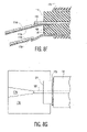
- FIG. 1A shows a portion of an AC electrical power transmission grid 10 that may be protected from an EEMP in accordance with the present invention.
- Grid 10 includes a power transmission line 12, suspended from transmission towers 14a and 14b, and may typically be much longer than as illustrated.
- Electrical transformers 16 and 18 are respectively situated at the two ends of power transmission line 12.
- Each transformer may comprise one phase of a 3-phase wye-connected transformer, by way of example.
- a lower-shown electrode of each transformer 16 and 18 is shown connected to a respective earth ground 20.
- each earth ground may comprise an electrical conductor buried in the ground to assure a more robust connection to earth ground.
- it may be desirable to inject a conductive agent into the ground such as a supersaturated solution of Copper Sulphate.
- FIG. 1B shows grid 10 of FIG. 1 , with transmission line 12 receiving an EEMP 22 of the nuclear electromagnetic pulse (NEMP) or non-nuclear electromagnetic pulse (NNEMP) variety. Pulse 22 is shown with associated arrows indicating direction of movement of the pulse. After being received by transmission line 12. NEMP or NNEMP 22 can follow either of two conductive paths 24 or 26 that respectively include transformers 16 and 18 and earth ground 20. NEMP or NNEMP 22 may typically induce current in conductive paths 24 or 26 far in excess of the current-handling capability of transformers 16 and 18, and would thereby render inoperative the transformers unless NEMP or NNEMP 22 is diverted away from them.
- NEMP nuclear electromagnetic pulse
- NNEMP non-nuclear electromagnetic pulse
- FIG. 1C shows grid 10 of FIG. 1 , with transmission line 12 receiving an EEMP of the geomagnetically-induced current (GIC) variety. Such pulse is shown at 28, with associated arrows showing direction of movement of the pulse.
- GIC pulse 28 can follow either of two conductive paths 30 or 32 that respectively include earth ground and transformers 16 and 18. GIC pulse 28 may typically induce current in conductive paths 30 or 32 far in excess of the current-handling capability of transformers 16 and 18, and would thereby render inoperative the transformers unless GIC pulse 28 is diverted away from them.
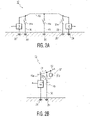
- FIG. 2A shows a simplified version of FIG. 1 with various current-diverting paths 36, 38 and 40.
- Current-diverting paths 36 and 38 respectfully divert current away from transformers 16 and 18.
- Optional current-diverting path 40 diverts current from a portion of transmission line 12, receptive of an EEMP, to prevent such portion of line 12 from being rendered inoperative by the EEMP.
- Each of paths 36, 38 and 40 constitutes a low-inductance, high current capacity circuit relative to the respective, associated electrical components of grid 10, and is shown diagrammatically as a switch 37a, 39a or 41a.
- an EEMP can be diverted from transformers 16 and 18 and from a portion of transmission line 12, receptive of an EEMP, before the EEMP can render such electrical components of the grid inoperative.
- FIG. 2B shows current-diverting path 36 of FIG. 2A in more detail.
- Current-diverting path 36 includes a protective device 37 consisting of a switch 37a and a switch controller 37b whose details are described below. It is desired for length 42, between an upper node 16a of transformer 16 and path 36, to be as short as is physically possible, so that the distance 43 between transformer 16 and current-diverting path 36 can be minimized. This is important to keep the risetime of the current-diverting path 36 fast enough to ensure the diversion circuit path is completed before the damaging pulse reaches the protected component. It may also be desirable to provide a vacuum capacitor (not shown) in parallel with current-diverting path 36, for suppressing ordinary EMP's, such as minor transients. This is true for the other current-diverting paths described herein.
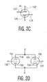
- switch 37a may be embodied as a bidirectional high-voltage cold-cathode field-emission bi-directional electron tube known as a Bi-tron 44.
- the name "Bi-tron” has been coined by the current inventor as a trademark, and its construction is described below.
- switch 37a may be embodied as a pair of back-to-back connected high-voltage cold-cathode field emissions triodes. The bi-directionality of switch 37a ( FIG. 2B ) allows the switch to turn on no matter what the polarity of the line voltage on transmission line 12 is relative to earth ground 20.
- switch 37a This prevents a delay in turning on switch 37a of up to 1 ⁇ 2 cycle for AC line voltage on transmission line 12.
- Bi-directionality of switch 37a is also desirable so that the switch conducts an EEMP that passes downwardly through transformer 16 (or other protected electrical component) as in FIG. 1B , or an EEMP that passes upwardly through transformer 16 (or other electrical component) as in FIG. 1C .
- the electrodes of Bi-tron 44 comprise first and second cathanodes 132 and 136, and first and second grids 102 and 110.
- the electrodes for each of high-voltage cold-cathode field emissions triodes 45a and 45b comprise an anode 100, a grid 102 and a cathode 104.
- either the Bi-tron of FIG. 2C or the back-to-back high-voltage cold-cathode field emission triodes of FIG. 2D are equally applicable to DC transmission lines as it is to AC transmission lines. This is due to the difference in current flow directions of EMP versus GIC pulses, as illustrated in FIGS. 1B and 1C , which requires bidirectional switching means. Both switches preferably have risetimes of less than 100 picoseconds, so as to protect against NEMP's and NNEMP's. Switches with significantly slower risetimes will not be effective in suppressing NEMP's and NNEMP's. Slower risetimes increase the likelihood of sustaining damage to the protected electrical components.
- an appropriate switch 37a for current-diverting path 36 has several design requirements: it must turn on before an EEMP can render inoperative the protected electrical components, i.e., transformers 16 and 18 in FIG. 2A , and it also must handle the high currents typical of EEMP's.
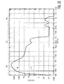
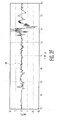
- FIGS. 2E and 2F respectively show typical waveforms for a nuclear electromagnetic pulse (NEMP) and an EEMP arising from geomagnetically-induced current.
- FIG. 2E shows a NEMP 46 and further shows sequential stages 46a, 46b and 46c of such NEMP.
- stage 46a for example, an NEMP 46 rises to well above 2Q volts per meter in field strength in less than 100 picoseconds. Pulses of this fast a risetime and with amplitudes equal to or greater than 20 volts per meter, whether NEMP or NNEMP, should be protected against. It is necessary to use a switching means with a risetime faster than 100 Picoseconds to prevent an electrical component from becoming inoperative due to NEMP 46 or an NNEMP (not shown).
- An acceptable risetime 47 is about 80 picoseconds. Risetimes significantly longer than 100 picoseconds are likely to allow damage to components sought to be protected. The likelihood increases as the risetime increases.
- the NEMP waveform 46 shown in FIG. 2E is a representative member of the class of waveforms commonly known as EMP, and more specifically as NEMP and NNEMP. These waveforms are each unique, but collectively share important common characteristics such as fast risetime. It is important to recognize that NEMP and NNEMP share common characteristics (e.g., risetime) and, from the point of view of the current invention and the protected electrical components, are indistinguishable.
- FIG. 2F shows a current-versus-time waveform for an EEMP 48 arising from a GIC pulse, and is an actual recording of a GIC that occurred January 13, 1999 in Finland. From FIG. 2F , it can be seen that either waveform is capable of inducing potentially damaging transients in an electrical power system.
- FIG. 3 illustrates protected electrical components having inputs or outputs floating with respect to earth ground as is found in delta-connected 3-phase circuits, for example.
- FIG. 3 shows an electrical generator 50 with a AC output appearing on output lines 50a and 50b, and a transformer 52 having its left-shown winding connected to lines 50a and 50b and having its output winding connected to output lines 52a and 52b.
- Lines 50a, 50b, 52a and 52b are all floating with respect to earth ground 20.
- Transformer 52 may comprise one phase of a 3-phase delta-connected winding, by way of example.
- current-diverting path 54 protects generator 50, while current-diverting path 56 protects the left-shown primary winding of transformer 52.
- current-diverting path 58 can provide a path for dissipation of current in line 50b through earth ground 20.
- the mentioned current-diverting paths conform to the above description of current-diverting paths, such as path 36 in FIG. 2B .
- Path 58 is especially desirable as it allows the circulating energy created by the two current-diverting paths to dissipate to ground.
- FIG. 4A shows one side 60 of wye-connected transformer windings 60a, 60b and 60c.
- Each winding 60a, 60b and 60c is shunted by an associated current-diverting path 62, 64 or 66, in accordance with an aspect of the invention.
- Paths 62, 64 and 66 are each shown in simplified form as a bi-directional switch of Bi-tron configuration, although control circuitry described below would be used to operate the Bi-tron switches.
- this wye-connected side 60 of a transformer one end of each of the windings and associated current-diverting paths is connected to earth ground 20.
- FIG. 4B shows one side 68 of delta-connected transformer windings 68a, 68b and 68c.
- Each winding 68a, 68b and 68c is shunted by an associated current-diverting path 70, 72 or 74 in accordance with an aspect of the invention.
- Paths 70, 72 and 74 are each shown in simplified form as a bi-directional switch of Bi-tron configuration, although control circuitry described below would be used to operate the Bi-tron switches.
- this delta-connected side 68 of a transformer neither end of the windings or of their associated current-diverting paths is connected to earth ground (not shown).
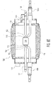
- FIGS. 5A and 5B illustrate a current-diverting path 78 that may be used in the case of wye-connected windings, as for instance, to implement in FIG. 4A current-diverting path 62, 64 or 66. As with paths 62, 64 and 66, current-diverting path 78 of FIG. 5A is connected to earth ground 20.
- current-diverting path 78 includes an electrically-insulated and vertically-supporting ground conductor 80, a vacuum housing 81, and an electrical and horizontally-supporting connection device 83 to a conductor 84 of an electrical power transmission grid.
- vacuum housing 81 preferably contains a switch, such as shown schematically in FIG. 2B at 37a, together with circuitry for detecting EEMP's.
- Insulated ground conductor 80 is preferably vertically self-supporting, with its lower end mechanically affixed to a mechanical support 88, shown diagrammatically.
- FIGS. 5B and 5C show more details of a preferred construction of electrical and horizontally-supporting connection device 83 of FIG. 5A , which minimizes the conductive path length from conductor 84 to EEMP detection circuitry within vacuum housing 81. This, in turn, decreases the risetime of the switch within housing 81.
- Housing 81 preferably comprises dielectric material that is optionally covered with a KEVLAR ® or similar aramid-fiber jacket 82 to make housing 81 more resistant to environmental hazards, such as sandstorms or being shot with a bullet.
- the connection to the power conductor 84 is made by a metal connector assembly 86, with metal connecting part 86e vacuum sealed to housing 81 at locations 86a, for instance.
- Metal connector assembly 86 includes clamps 86b, 86c and 86d for clamping onto conductor 84, which fits within a generally V-shaped groove 86f, wherein any sharp edges have been removed. Clamps 86b, 86c and 86d may be held onto metal connecting part 86e with appropriate screws 86g, for instance.
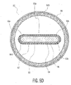
- FIG. 5D is a cross-sectional view of insulated ground conductor 80 taken at arrows 5D, 5D in FIG. 5A .
- Insulated ground conductor 80 has an inner part 80a and outer part 80b.
- Inner part 80a preferably comprises an elongated, conductive stainless steel core 90, encircled by a conformal conductive chrome sheathing layer 92, which in turn is covered by a conformal conductive copper sheathing layer 94.
- Sheathings 92 and 94 are preferably applied by the plasma-spray process. Alternatively, sheathings 92 and 94 could be applied as thick electroplated layers.
- a corrosion-resistant dielectric protective layer 96 covers copper sheathing layer 94.
- Protective layer 96 is preferably applied by electrostatic powder coating.
- a KEVLAR ® or similar aramid-fiber jacket 99 preferably encases outer part 80b to provide resistance against environmental hazards, such as sandstorms or being shot with a bullet.
- chrome sheathing layer 92 should intimately conform to stainless steel core 90, and copper sheathing layer 94 should intimately conform to chrome sheathing layer 92.
- stainless steel core 90 preferably should have a vertical-to-horizontal dimension in FIG. 5D exceeding 10:1, and the edges 98a, 98b, 98c and 98d of inner part 80a of insulated ground conductor 80 are preferably radiused such that the radius equals approximately half the vertically shown dimension of core 90 and layers 92 and 94.
- Outer part 80b of insulated ground conductor 80 preferably comprises ceramic or terra cotta or other dielectric material having resistance to high temperatures. This is necessary due to high current level through conductor 80 which can, in some extreme cases, cause said ground conductor 80 to heat up due to I2R heating.
- FIGS. 6A and 6B show basic structure of the high-voltage cold-cathode field emission triode 45a (or 45b) of FIG. 2D , also known as a Pulsatron as described in USP 4,950,962 by the current inventor and others. However, the Pulsatron is scaled in size to operate in the continuous mode at a desired voltage.
- Triode 45a includes a cylindrically shaped cathode 100 which is encircled by a cylindrically shaped grid 102, which in turn is encircled by a cylindrically shaped anode 104.
- Grid 102 is shown as dashed lines to indicate that it would have suitable holes for passage therethrough of electrons.
- the anode 104, grid 102 and cathode 100 share a common main axis (not shown).
- the radial spacing from cathode 100 to grid 102 is such as to create therebetween a circular waveguide supporting the transverse electromagnetic mode (TEM).
- TEM transverse electromagnetic mode
- the cathode 100 is comprised of a graphite material
- the grid 102 is comprised of a conductive metal such as stainless steel
- the anode 104 is comprised of a refractory metal such as tungsten, by way of example.
- FIGS. 6C and 6D shows basic structure of the high-voltage cold-cathode field emission tube 44 of FIG. 2C , also known as a Bi-tron as mentioned above.
- Bi-tron 44 includes a cylindrically shaped electrode 106, referred to herein as a cathanode; that is, an electrode that can function as either a cathode or an anode. Encircling cathanode 106 (referred to as first cathanode 132 in FIG.
- first grid 102 is a cylindrically shaped first grid 102, which in turn is encircled by a cylindrically shaped second grid 110, which is then encircled by a cylindrically shaped cathanode 112 (referred to as a second cathanode 136 in FIG. 2C ).
- First and second grids 102 and 110 are shown as dashed lines to indicate that they would have suitable holes for passage therethrough of electrons.
- the cathanodes 106 and 112, and the first and second grids 102 and 110 share a common main axis (not shown).
- the radial spacfing from cathanode 106 to grid 102 is such as to create therebetween a circular waveguide supporting the transverse electromagnetic mode (TEM).
- TEM transverse electromagnetic mode
- the radial spacing from cathanode 112 to grid 110 is such as to create therebetween a circular waveguide supporting the transverse electromagnetic mode (TEM).
- the radial spacing between the first grid 102 and the second grid 110 is sufficient to prevent flashover therebetween at an intended operating voltage.
- the cathanodes 106 and 112 are comprised of a graphite material and the grids 102 and 110 are comprised of a conductive metal such as stainless steel, by way of example.
- Both the triode 45a of FIGS. 6A and 6B and the Bi-tron 44 of FIGS. 6C and 6D beneficially can handle current levels of 400 Amps per square centimeter.
- the speed of each of these switches is preferably enhanced by so-called top-hat sockets described below.
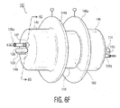
- FIG. 6E shows a Bi-tron 162, which is a form of bidirectional high-voltage cold-cathode field-emission electron tube.
- Tube 162 includes an electrically-insulated housing 116, first and second cathanodes 132 and 136 (referred to as 106 and 112 in FIG. 6C ) mounted on respective first and second cathanode connectors 134 and 138.
- First and second grids 102 and 110 are mounted on respective grid feedthroughs 126a and 126b.
- a chemical getter pump 118 is mounted on getter pump feedthrough 120 and is used to maintain the vacuum in the housing 116 during periods when no electric power is available.
- a vacuum exhaust tipoff 122 is created at the end of the manufacturing cycle and is used to seal off the housing 116 from the manufacturing equipment.
- the electron tube 168 shown in FIGS. 6A, 6B , and the electron tube 162 shown in FIGS. 6C, 6D are designed for a substantially higher operating voltage, and hence have a different aspect ratio, than the electron tube shown in FIG. 6E .
- FIG. 6F shows a reentrant tube socket 142, which lowers the inductance of connections to a Bi-tron 162 or a Pulsatron 168 electron tube and reduces risetime of the switch by a factor that may typically be 6:1.
- This tube socket 142 is primarily designed for use with parallel plate transmission lines, although it can be successfully integrated into other circuit configurations.
- Reentrant tube socket 142 comprises preferably identical conductive top-hat shaped members 144 and 146 that respectively enclose the two longitudinal ends of the electrically-insulated housing 116 shown in FIG. 6E .
- Each conductive top-hat shaped member 144 and 146 has a respective rim 144a or 146a for connecting to external circuitry.
- FIG. 6G Electrical connection from circuitry within electrically-insulated housing 116 to members 144 and 146 may be accomplished as shown in FIG. 6G .
- conductive tab 150 of member 144 interconnects with the cathanode connector 138 by means of a mounting screw 151.
- Conductive tab 150 is connected to the first or second cathanode connector 134 or 138.
- the combination of the conductive mounting tab 150 and mounting screw 151 also provide a mechanical interconnection between top hat shaped member 144 or 146 and the electron tube 162 or 168.
- the conductive mounting tab 150 is preferably welded to the top of the conductive top-hat shaped members 144 and 146.
- clearance holes e.g., 147) and slots (e.g., 149) in the top-hat shaped members 144 and 146 are required to accommodate electrical connections such as grid feedthrough 126 on electron tubes 162 or 168.
- Rims 144a and 146a are spaced apart from each other to prevent flashover between them. If desired, an additional insulator 212 ( FIG. 10 ) described below can be placed between the rims, which further lowers the inductance of connections to the switch, thus further decreasing risetime of the switch.
- FIG. 7 shows a DC threshold detector circuit 152, which implements a current-diverting path 154 with a control circuit for protecting against an NEMP or NNEMP in a conductive path normally at a DC voltage.
- Path 154 includes a unidirectional switch, comprising a high-voltage cold-cathode field emission triode 168, known as a Pulsatron tube and associated control circuitry. Tube 168 is biased to a standoff condition (i.e., not conducting) at normal line voltage plus an acceptable excess voltage. When the excess voltage value is exceeded, the threshold detector circuit 152 causes the tube 168 to go into conduction so as to create current-diverting path 154.
- the tube 168 is biased to shut-off by the network composed of resistors R1 and R2, which form a voltage divider.
- Resistors R1 and R2 establish a grid voltage that is proportional to the voltage on line.
- the tube is oriented appropriately to the polarity of the transmission line to which it is attached.
- the schematic shown is for a negative polarity line.
- the resistor R1 is a relatively low value resistor and resistor R2 is a relatively high value resistor. This places the grid close to the cathode potential. This relationship is maintained in all Pulsatron and Bi-tron circuits described below in connection with FIGS.
- the resistors with an odd reference numeral i.e., 1, 3 and 5
- the resistors with an odd reference numeral preferably are adjustable resistors, as diagrammatically shown. The specific values are dependent on the voltage at which the circuit operates.
- the capacitor C1 is used to maintain the control voltage if the line voltage goes low for a short period. This is also true for capacitors C2 and C3 in FIGS. 8A-8B .
- the tube 168 starts conducting.
- the threshold level is chosen so that the presence of an NEMP or NNEMP in a conductive path (not shown) including a protected electrical component is detected prior to the pulse reaching and rendering inoperative such electrical component. Accordingly, current-diverting path 154 with tube 168 diverts the NEMP or NNEMP around the protected electrical component with a low inductance, high current capacity circuit relative to the electrical component, before the pulse can reach and render the electrical component inoperative.
- FIG. 8A shows a current-diverting path 160 with control circuitry for protection against an NEMP or NNEMP in a conductive path normally at an AC voltage.
- a bidirectional Bi-tron 162 is used rather than the unidirectional Pulsatron tube 168 of FIG. 7 .
- a second voltage divider R3-R4 and capacitor C2 are included. The operation of the detection of NEMP or NNEMP and diverting current away from a protected component as described in connection with FIG. 7 apply to FIG. 8A , except for the duplication of the control network to accommodate AC operation.
- FIG. 8A also shows a high-speed current shunt 164 in the ground leg of the circuit. This shunt provides an output when the Bi-tron 162 conducts. This output on node 166 can be used to advise system operators of an EEMP event, or as a means of triggering other protective circuitry.
- FIG. 8B shows a preferred control circuit 167.
- Circuit 167 is similar to FIG. 8A , but shows a GIC detection circuit 169 for detecting a GIC.
- the GIC detection circuit 169 comprises voltage-divider network R5-R6 and capacitor C3, together with a Pulsatron 168.
- the current traversing current shunt 164 develops a voltage proportional to the magnitude of the current and its temporal waveform. Such voltage triggers Pulsatron 168 into conduction.
- FIG. 8C shows high speed current shunt 164, which is comprised of a flat conductive metal strap 170, with connection holes 170a for connection to a ground path of an external circuit.
- Metal strap 170 is preferably made of copper or having conductivity at least as low as commercial grade copper. "Commercial grade" connotes copper refined to at least 94 percent copper by mass.
- Copper strap 170 preferably has fully radiused ends 170b, with holes 170a for respective connections to node 172, also shown in FIGS. 8A and 8B , and earth ground 20. Holes 170a are provided for electrical connection purposes. Preferably, the edges of copper strap 170 are deburred and radiused.
- Current shunt 164 has the ability to measure pulse currents in excess of 100,000's of Amps.
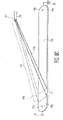
- FIG. 8C also shows a tapered parallel-plate transmission-line matching transformer 174 being preferably silver-soldered to copper strap 170 at the dual ends of a defined current measuring region 171.
- the narrow ends of plates 174a and 174b in transmission line 174 are preferably silver-soldered to an end 173 of a 50-ohm coaxial cable 176.
- Coaxial cable 176 must be at least about 1 ⁇ 2-inch (12.77 mm) in diameter to handle the high voltage that results from large amounts of current across the measuring region 171. Increasing amounts of currents force the use of progressively larger diameter coaxial cable to handle the increased voltage produced by the measuring region 171 of the shunt 164.
- the width of each of plates 174a and 174b at their connection junctures to metal strap 170 is preferably approximately the same, although these widths may vary from about 0.9 to 1.1 times the width of the strap 170.
- the ratio of the length of upper plate 174a to the width of the flat metal strap 170 preferably is approximately 10 to 1. Lower ratios lead to increasing impedance mismatch. Having a ratio substantially larger than 10 to 1 leads to an overly large and ungainly structure.
- plates 174a and 174b can have various tapers from their narrow ends to their wide ends. For example, the simplest taper is a straight line so that the plates approximate equilateral triangles. A preferred taper is more complex so as to have exponentially varying sides to the foregoing equilateral triangle, approximating the curve of the bell (or output orifice) of a musical trombone.
- FIG. 8D shows a side view of copper strap 170, upper and lower plates 174a and 174b of transmission line 174, and insulation 178a and 178b. Such insulation 178a and 178b are omitted from FIG. 8C for clarity of illustration.
- Insulation 178a extends the entire length under first plate 174a, from the juncture of the copper strap 170 and the wide end of upper plate 174a to an end in slot 188 in the center insulation 177 ( FIG. 8E ) of a coaxial cable 176.
- Slot 188 ( FIG. 8E ) serves the function of eliminating a line-of-sight path for electrons to prevent a short circuit from forming between center conductor 182 and coaxial shield 186.
- Insulation 178b preferably extends a minimum of one-half the length of lower plate 174b under such plate from the juncture of the copper strap 170 and the wide end of lower plate 174b.
- FIG. 8E shows the tapered parallel-plate transmission line 174 connected to coaxial cable 176.
- the center conductor 182 of the coaxial cable 176 is soldered (as shown by a solid black region) to the upper side of the upper plate 174a.
- coaxial cable shield 186 shown with an enlarged view of braids of wires forming the shield, is soldered (as shown by a solid black region) to the underside of lower plate 174b.
- the foregoing solder connections are made using silver solder with a silver content exceeding approximately 5 percent by mass.
- FIG. 8F shows transmission line 174 with upper plate 174a preferably silver-soldered to center conductor 182 and lower plate 174b preferably silver-soldered to shield 186 of coaxial cable 176. As mentioned above, insulation 178a is inserted into slot 188 in center insulation 177 of cable 176.
- FIG. 8G shows first plate 174a silver-soldered to center conductor 182 in cable 176. Insulation 178a can be seen protruding from under first plate 174a.
- the foregoing current shunt 164 of FIGS. 8C-8G can be arranged with the upper and lower plates 174a and 174b functionally interchanged.
- the upper plate 174a was the "hot" conductor and the lower plate 174b was the "ground” conductor.
- these functions are interchanged so that the upper plate becomes the ground conductor and is attached to the shield 186 of coaxial cable 176, and the lower plate becomes the hot conductor and is attached to the center conductor 182 of coaxial cable 176.
- the insulation 178b is now inserted into slot 188 of coaxial cable 176.
- the current shunt output must be corrected for high frequency operation due to the skin effect on resistance.
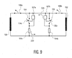
- FIG. 9 shows a pair of protected electrical components 190 and 192 with associated current-diverting paths 194 and 196 including protective devices 194a and 196a and preferably a pair of normally-closed series switches 198a and 198b.
- Components 190 and 192 may be windings of a transformer or an electrical generator, by way of example.
- the protective devices 194a and 196a in current-diverting paths 194 and 196 are examples of protective device 37 of FIG. 2B .
- Normally-open switches in protective devices 194a and 196a close upon detection of an EEMP event.
- NEMP and NNEMP events are detected as voltages preferably by control circuit 167a and 167b (see 167 in FIG. 8B ), and GIC events are detected as currents by current shunts 164a and 164b operating in conjunction with control circuits 167a and 167b as shown in FIG. 9 .
- control circuit 167a Upon receipt of suitable voltage or current inputs, control circuit 167a outputs a control signal to activate normally-closed switch 198a. Similarly, upon receipt of suitable voltage or current inputs, control circuit 167b outputs a control signal to activate normally-closed switch 198b.
- the closing of the normally-open switches in response to control signals from control circuits 167a and 167b cause devices 194a and 196a to collapse the magnetic field in windings 190 and 192, and create current-diverting paths 194 and 196, respectively.
- the switches in the protective devices 194a and 196a also produce an output that is used to trigger the opening of normally-closed switches 198a and 198b after a predetermined time after detection of an EEMP of no more than two cycles of the line voltage. This is for the purpose of removing a short circuit from protected component 190.
- Arrows 200 show the circulating path of current produced by the EEMP event in the current-diverting paths 194 and 196. The direction the foregoing current depends on instantaneous polarity of the circuit at the time of the EEMP event, and may or may be in the direction of the arrowheads as shown.
- the normally-closed switches 198a and 198b of FIG. 9 may be any type of switch with suitable voltage, current, and response-time ratings, which would include a Bi-tron 44 or 162 ( FIG. 2C or FIG. 6E ).
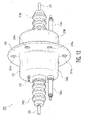
- FIG. 10 shows a complete EEMP protection device 204, which is the preferred embodiment of the FIG. 8B electrical schematic for wye-connected electrical components.
- the device 204 has two types of internal vacuum pumps. One is a chemical getter pump 118. This is always functional. The second is an ion pump 206 of conventional design but of open construction for maximum conductivity. There is an internal magnetic shielding 208 to preclude interference with the electron trajectories in the adjacent switch tube 162 of FIG. 10 or switch tube 168 (not shown). While the ion pump 206 requires a small amount of electricity to operate, it is critical to ensure that the vacuum is properly maintained at all times in the enclosure.
- the chemical getter pump 118 maintains the vacuum when electricity is not available, such as during shipping, installation, maintenance or blackouts.
- switch tube 162 or 168 mounted inside the reentrant tube socket 142.
- Top-hat shaped sockets 144 and 146 are separated by an insulator wall 212.
- This wall 212 serves the dual purpose of providing additional electrical insulation between the two sockets 144 and 146 and simultaneously provides a mechanical mounting means for the tube 162 or 168 and reentrant tube socket 142.
- the preferred control circuit 167 is connected to the electrodes of tubes 162 and 168.
- One of the electrical connection leads, 210a runs through an insulated feedthrough tube 210 to allow an insulated electrical connection to electrodes of switch tube 162 or 168 on the other side of insulated wall 212.
- one embodiment includes the concept of not having such tubes 162 or 168 in individual vacuum housings, such as housing 116 ( FIG. 6E ). Instead, the tubes are constructed in open housings and use the vacuum system 206 instead to maintain the vacuum necessary for their operation.
- the insulated ground conductor 80 previously described in FIG. 5D has one end terminated inside the housing 81.
- the ground conductor 80 may serve two functions: when used with an electrical component with windings in a wye configuration, it provides mechanical support for the EEMP protection device 204 by supporting the entire weight of said system, and it simultaneously provides a low-inductance path to ground 20 to allow completion of the current-diverting path during operation.
- the ground connection means is connected to the balance of the circuitry via the current shunt 164 ( FIGS. 8C-8G ).
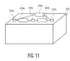
- FIG. 11 shows one set of connections of a delta-configured transformer 220.
- the terminations for the windings of the transformer 220 are presented as bushings 222a, 222b, and 222c.
- Three EEMP protection devices 204 are positioned side by side and are wired to place each device 204 between a respective pair of terminals constituting a single phase of the transformer 220 winding.
- device 204a is connected to bushings 222a and 222b
- device 204b is connected to bushings 222b and 222c
- device 204c is connected to bushings 222c and 222a as shown in FIG.11 .
- EMP protective devices For protection of a power system, it is necessary to protect the primary and secondary of every transformer of that system with an EMP protective device 204 installed physically adjacent to the transformer on each phase connection. It is further necessary to similarly protect generators of the power system with EMP protective devices on each phase connection installed physically adjacent to the generator itself. For economic or other reasons, EMP protective devices may be used with fewer than all transformers and generators of a power system.
- FIG. 12 shows a Bi-tron tube 225, contained within vacuum-sealed conductive housing 236 having sections 236a and 236b.
- Housing sections 236a and 236b are continuously tungsten-inert gas (TIG) welded to a conductive flange 234 by weld beads 237.
- TIG tungsten-inert gas
- the flange 234 can be mounted to the exterior, conductive wall of a shielded room or building, by way of example.
- a common conductive element generally marked as 232 passes entirely through the tube 225, passing through primary electrical insulators 230a and 230b.
- the central conductive element 232 is connected the incoming power line (not shown) and is referred to hereinafter as "line”.
- the central conductive element 232 is connected the protected component (not shown) and is referred to hereinafter as "load”.
- Element 232 supports the first cathanode 106 on its exterior surface.
- Element 232 preferably has a conductivity at least as high as that of Type 304 stainless steel.
- Various internal electrical insulators are provided as required, as will be apparent to persons of ordinary skill in the art based on the present specification.
- FIG. 13 shows an exemplary perspective view of the Bi-tron tube 225 of FIG. 12 .
- Bi-tron 162 of FIGS. 6E and 6F is primarily intended for use with primary power grid components such as generators and substation transformers.
- Bi-tron 225 of FIGS. 12 and 13 is primarily intended for use as a shielded feedthrough and an RF- and EMP-diverting component for use with EMP shielded rooms and buildings.
- the flange 234 mount provides a convenient and easily implemented technique for achieving a fully symmetrically ground connection to an electrically shielded wall. Thus, installation of Bi-tron 225 involves no special skills, merely requiring the skills of a journeyman electrician for installation.
- the mounting flange 234 has two bolt circles; the outer bolt circle of holes 234a is used for physically mounting and installing the Bi-tron 225.
- the inner circle of holes 234b is inside the vacuum enclosure 236a, 236b and provides vent holes between the respective housing sections 236a and 236b on either side of the flange 234.
- the flange 234 also contains a threaded boss 238 to which the outer cathanode 112 is mounted.
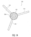
- a low pass filter comprising at least a bypass capacitor 240 may be advantageously incorporated into Bi-tron 225 for reducing minor RF transient signals that are below the turn-on threshold of Bi-tron 225. Additional or alternative RF filtering components may be incorporated in the vicinity of the illustrated location of the bypass capacitor 240.
- One plate 232c of the bypass capacitor 240 may be formed by enlarging conductive element 232, as shown.
- a second plate 242 of the capacitor 240 may comprise a conductive tubular electrode, which is mechanically suspended from, and electrically connected to, either the housing section 236b as shown, or from the housing section 236a or both housing sections 236a and 236b, as shown best in FIG. 14 .
- Second plate 242 of the capacitor 240 may be mechanically suspended from, and electrically connected to, the housing section 236b by a support structure such as spokes 244.
- the spokes 244 are welded to the housing section 236b and may integrally formed with the second plate 242.
- the Bi-tron control circuitry contains a number of discrete electrical components (e.g., R1, R2, C1, C2 etc.). While it is preferable that these components be mounted externally to the vacuum enclosure of Bi-tron 162 (e.g., FIG. 6E ) or of Bi-tron 225 (e.g., FIG. 12 ), it is possible to physically locate some or all of these components inside the vacuum enclosure 236 of FIG. 12 or 116 of FIG. 6E .
Landscapes
- Physics & Mathematics (AREA)
- High Energy & Nuclear Physics (AREA)
- Emergency Protection Circuit Devices (AREA)
- Microwave Tubes (AREA)
- Particle Accelerators (AREA)
Applications Claiming Priority (4)
| Application Number | Priority Date | Filing Date | Title |
|---|---|---|---|
| US12/554,818 US8248740B2 (en) | 2008-09-19 | 2009-09-04 | High speed current shunt |
| PCT/US2009/056124 WO2010047890A2 (en) | 2008-09-19 | 2009-09-04 | Method and apparatus for protecting power systems from extraordinary electromagnetic pulses |
| EP10814101.1A EP2474077B1 (en) | 2009-09-04 | 2010-03-09 | Method and apparatus for protecting power systems from extraordinary electromagnetic pulses |
| PCT/US2010/026708 WO2011028300A1 (en) | 2009-09-04 | 2010-03-09 | Method and apparatus for protecting power systems from extraordinary electromagnetic pulses |
Related Parent Applications (3)
| Application Number | Title | Priority Date | Filing Date |
|---|---|---|---|
| EP10814101.1A Division EP2474077B1 (en) | 2009-09-04 | 2010-03-09 | Method and apparatus for protecting power systems from extraordinary electromagnetic pulses |
| EP10814101.1A Division-Into EP2474077B1 (en) | 2009-09-04 | 2010-03-09 | Method and apparatus for protecting power systems from extraordinary electromagnetic pulses |
| PCT/US2010/026708 Previously-Filed-Application WO2011028300A1 (en) | 2008-09-19 | 2010-03-09 | Method and apparatus for protecting power systems from extraordinary electromagnetic pulses |
Publications (3)
| Publication Number | Publication Date |
|---|---|
| EP3758181A2 EP3758181A2 (en) | 2020-12-30 |
| EP3758181A3 EP3758181A3 (en) | 2021-01-13 |
| EP3758181B1 true EP3758181B1 (en) | 2022-05-04 |
Family
ID=43661796
Family Applications (2)
| Application Number | Title | Priority Date | Filing Date |
|---|---|---|---|
| EP10814101.1A Active EP2474077B1 (en) | 2009-09-04 | 2010-03-09 | Method and apparatus for protecting power systems from extraordinary electromagnetic pulses |
| EP20162042.4A Active EP3758181B1 (en) | 2009-09-04 | 2010-03-09 | Bidirectional high-voltage cold-cathode field-emission vacuumelectron tube |
Family Applications Before (1)
| Application Number | Title | Priority Date | Filing Date |
|---|---|---|---|
| EP10814101.1A Active EP2474077B1 (en) | 2009-09-04 | 2010-03-09 | Method and apparatus for protecting power systems from extraordinary electromagnetic pulses |
Country Status (7)
| Country | Link |
|---|---|
| US (1) | US8248740B2 (enExample) |
| EP (2) | EP2474077B1 (enExample) |
| JP (1) | JP5362116B2 (enExample) |
| KR (1) | KR101426743B1 (enExample) |
| CA (1) | CA2772219C (enExample) |
| NZ (1) | NZ598388A (enExample) |
| WO (1) | WO2011028300A1 (enExample) |
Families Citing this family (30)
| Publication number | Priority date | Publication date | Assignee | Title |
|---|---|---|---|---|
| US9077172B2 (en) | 2012-05-21 | 2015-07-07 | Emprimus, Llc | Self-testing features of sensing and control electronics for a power grid protection system |
| US8878396B2 (en) | 2010-07-20 | 2014-11-04 | Emprimus, Llc | Continuous uninterruptable AC grounding system for power system protection |
| US8537508B2 (en) | 2010-07-20 | 2013-09-17 | Emprimus, Llc | Sensing and control electronics for a power grid protection system |
| USRE48775E1 (en) | 2010-07-20 | 2021-10-12 | Techhold, Llc | Self-testing features of sensing and control electronics for a power grid protection system |
| JP5908913B2 (ja) | 2010-10-05 | 2016-04-26 | アドバンスト フュージョン システムズ エルエルシー | 高電圧・大電流調整回路 |
| WO2013149600A1 (es) * | 2012-04-02 | 2013-10-10 | Arnedo Gonzalez Luis Raul | Equipo eléctrico formado por una bobina en corto circuito flotante |
| ES2430403B2 (es) * | 2012-05-18 | 2014-08-22 | Universidad De La Rioja | Dispositivo y procedimiento de aislamiento de torres de tendidos aéreos |
| US9564753B2 (en) | 2012-05-21 | 2017-02-07 | Emprimus, Llc | Transformer protection circuit and method |
| CN103545803B (zh) * | 2013-10-31 | 2016-08-17 | 广东威创视讯科技股份有限公司 | 设备电源接口电路保护装置 |
| US9728967B2 (en) * | 2014-03-24 | 2017-08-08 | Advanced Fusion Systems Llc | System for improving power factor in an AC power system |
| KR101622463B1 (ko) | 2014-05-13 | 2016-05-18 | 엘에스산전 주식회사 | 고전압 직류 송전 시스템의 절연 설계 장치 및 방법 |
| KR101639863B1 (ko) * | 2014-05-13 | 2016-07-14 | 엘에스산전 주식회사 | 고전압 직류 송전 시스템을 설계하는 장치 및 방법 |
| AU2015274548B2 (en) | 2014-06-11 | 2017-02-16 | Asator Global Technologies Llc | Surge suppression system for medium and high voltage |
| US10165405B2 (en) | 2014-11-28 | 2018-12-25 | Joel Ho | EMP-shielded, power-independent SMS text tower system for nuclear communications |
| ES2926134T3 (es) | 2015-01-06 | 2022-10-24 | Techhold Llc | Sistemas y métodos para la actuación de un sistema de bloqueo del neutro de un transformador |
| EP3394874B1 (en) * | 2015-12-22 | 2025-08-20 | Thermatool Corp. | High frequency power supply system with closely regulated output for heating a workpiece |
| CN106446372A (zh) * | 2016-09-12 | 2017-02-22 | 广东电网有限责任公司电力科学研究院 | 一种三相变压器a相短路状态下电磁场的计算方法及装置 |
| US10985559B2 (en) | 2017-02-03 | 2021-04-20 | Techhold Llc | Method and system for improved operation of power grid components in the presence of direct current (DC) |
| US11451047B2 (en) | 2017-03-30 | 2022-09-20 | Techhold, Llc | Protection of electrical devices based on electromagnetic pulse signal |
| US10530151B2 (en) * | 2018-01-09 | 2020-01-07 | Timothy A Carty | System and method for suppressing electromagnetic pulse-induced electrical system surges |
| JP6534466B1 (ja) * | 2018-02-26 | 2019-06-26 | ソフトバンク株式会社 | 電磁パルス防護システム、電子機器及び電磁パルス防護方法 |
| CN109167407B (zh) * | 2018-09-19 | 2022-08-05 | 武汉大学 | 一种架空地线取能系统 |
| US11114856B2 (en) * | 2020-01-27 | 2021-09-07 | Advanced Fusion Systems Llc | Method and apparatus for protecting electrical components from a transient electromagnetic disturbance |
| US11322814B2 (en) | 2020-01-27 | 2022-05-03 | Advanced Fusion Systems Llc | Method and apparatus for protecting electrical components from a transient electromagnetic disturbance transmitted on parallel power lines |
| IL309304A (en) * | 2020-10-09 | 2024-02-01 | Enertechnos Ltd | transmits electrical power |
| US11329480B1 (en) * | 2021-03-05 | 2022-05-10 | Advanced Fusion Systems Llc | Series static spark gap for EMP protection |
| CA3211469A1 (en) * | 2021-03-17 | 2022-09-22 | Curtis A. Birnbach | Method and apparatus for protecting electrical components from a transient electromagnetic disturbance transmitted on parallel power lines |
| US12253552B2 (en) | 2021-10-01 | 2025-03-18 | Faraday Defense Corporation | Apparatus for detection of electrical disturbances resulting from electromagnetic pulse |
| GB2619295B (en) * | 2022-05-30 | 2024-07-03 | Energy Res Lab Ltd | EMP protection system |
| US20240339827A1 (en) * | 2023-04-04 | 2024-10-10 | Timothy A Carty | System and method for suppressing electromagnetic pulse-induced electrical system surges |
Family Cites Families (25)
| Publication number | Priority date | Publication date | Assignee | Title |
|---|---|---|---|---|
| US4594630A (en) * | 1980-06-02 | 1986-06-10 | Electric Power Research Institute, Inc. | Emission controlled current limiter for use in electric power transmission and distribution |
| US4443672A (en) * | 1982-02-11 | 1984-04-17 | International Telephone & Telegraph Corporation | Low capacitance radio frequency switch |
| US4554608A (en) * | 1982-11-15 | 1985-11-19 | Block Roger R | Connector for electromagnetic impulse suppression |
| US4546358A (en) * | 1984-01-19 | 1985-10-08 | The United States Of America As Represented By The Secretary Of The Army | Large broadband free radiating electromagnetic test cell |
| US4723263A (en) * | 1985-05-20 | 1988-02-02 | Quantum Diagnostics, Ltd. | X-ray source |
| US4950962A (en) | 1985-05-20 | 1990-08-21 | Quantum Diagnostics, Ltd. | High voltage switch tube |
| US4809011A (en) * | 1985-06-14 | 1989-02-28 | Kunz Associates, Inc. | Electronically steerable antenna apparatus |
| US4807081A (en) * | 1986-09-05 | 1989-02-21 | Raychem Limited | Circuit protection arrangement |
| US4912589A (en) * | 1988-01-13 | 1990-03-27 | Tii Industries, Inc. | Surge suppression on AC power lines |
| US5502354A (en) * | 1992-07-31 | 1996-03-26 | Correa; Paulo N. | Direct current energized pulse generator utilizing autogenous cyclical pulsed abnormal glow discharges |
| US5905623A (en) * | 1997-05-27 | 1999-05-18 | Oneac Corporation | Telephone and data overvoltage protection apparatus including a longitudinal transformer |
| US6061223A (en) * | 1997-10-14 | 2000-05-09 | Polyphaser Corporation | Surge suppressor device |
| AU740311B2 (en) | 1998-02-17 | 2001-11-01 | Huber & Suhner Ag | EMP - charge eliminator |
| JP4042210B2 (ja) * | 1998-05-28 | 2008-02-06 | 株式会社デンソー | 電磁スイッチ |
| JP2000125461A (ja) * | 1998-08-11 | 2000-04-28 | Hitachi Ltd | 変電システム及びその制御方法 |
| US6636407B1 (en) * | 2000-09-13 | 2003-10-21 | Andrew Corporation | Broadband surge protector for RF/DC carrying conductor |
| US6433557B1 (en) | 2000-12-21 | 2002-08-13 | Eaton Corporation | Electrical system with capacitance tap and sensor for on-line monitoring the state of high-voltage insulation and remote monitoring device |
| SE527406C2 (sv) * | 2004-05-10 | 2006-02-28 | Forskarpatent I Syd Ab | Förfarande och DC-avledare för skydd av kraftsystem mot geomagnetiskt inducerade strömmar |
| US20060082946A1 (en) * | 2004-10-14 | 2006-04-20 | Rain Bird Corporation | Power surge protection in an irrigation controller |
| JP4715371B2 (ja) * | 2005-07-29 | 2011-07-06 | Tdk株式会社 | サージ吸収素子及びサージ吸収回路 |
| US7561387B2 (en) | 2005-10-19 | 2009-07-14 | Eaton Corporation | Current transformer including a low permeability shunt and a trip device employing the same |
| JP5053579B2 (ja) | 2006-06-28 | 2012-10-17 | 寛治 大塚 | 静電気放電保護回路 |
| US20080038871A1 (en) | 2006-08-10 | 2008-02-14 | George Liang-Tai Chiu | Multipath soldered thermal interface between a chip and its heat sink |
| US7612733B2 (en) * | 2007-03-12 | 2009-11-03 | The Regents Of The University Of Colorado | Transition region for use with an antenna-integrated electron tunneling device and method |
| EP2243210B1 (en) * | 2008-01-24 | 2017-03-22 | Advanced Fusion Systems LLC | High voltage inverter |
-
2009
- 2009-09-04 US US12/554,818 patent/US8248740B2/en active Active
-
2010
- 2010-03-09 NZ NZ598388A patent/NZ598388A/xx unknown
- 2010-03-09 EP EP10814101.1A patent/EP2474077B1/en active Active
- 2010-03-09 WO PCT/US2010/026708 patent/WO2011028300A1/en not_active Ceased
- 2010-03-09 CA CA2772219A patent/CA2772219C/en active Active
- 2010-03-09 JP JP2012527869A patent/JP5362116B2/ja active Active
- 2010-03-09 EP EP20162042.4A patent/EP3758181B1/en active Active
- 2010-03-09 KR KR1020127008260A patent/KR101426743B1/ko active Active
Also Published As
| Publication number | Publication date |
|---|---|
| EP3758181A2 (en) | 2020-12-30 |
| NZ598388A (en) | 2013-09-27 |
| WO2011028300A1 (en) | 2011-03-10 |
| EP2474077B1 (en) | 2020-04-29 |
| JP5362116B2 (ja) | 2013-12-11 |
| US20100097734A1 (en) | 2010-04-22 |
| CA2772219A1 (en) | 2011-03-10 |
| JP2013504297A (ja) | 2013-02-04 |
| KR20120099393A (ko) | 2012-09-10 |
| US8248740B2 (en) | 2012-08-21 |
| CA2772219C (en) | 2013-10-15 |
| EP2474077A4 (en) | 2014-05-14 |
| EP3758181A3 (en) | 2021-01-13 |
| EP2474077A1 (en) | 2012-07-11 |
| KR101426743B1 (ko) | 2014-08-06 |
Similar Documents
| Publication | Publication Date | Title |
|---|---|---|
| EP3758181B1 (en) | Bidirectional high-voltage cold-cathode field-emission vacuumelectron tube | |
| US8300378B2 (en) | Method and apparatus for protecting power systems from extraordinary electromagnetic pulses | |
| EP2590200B1 (en) | High speed current shunt | |
| JP7325440B2 (ja) | 電磁パルスにより誘導された電気系統のサージを抑制するシステムおよび方法 | |
| AU2011201033B2 (en) | Method and apparatus for protecting power systems from extraordinary electromagnetic pulses | |
| CA2338566C (en) | Creeping discharge lightning arrestor | |
| US6957117B2 (en) | Portable protective air gap tool and method | |
| AU2013201213B2 (en) | High speed current shunt | |
| Piparo et al. | Performance evaluation of a coordinated surge protective devices system | |
| JPH05111152A (ja) | ビル接地システム及び接地極間連結放電安全器 | |
| Sueta et al. | Protection of Low-Voltage Equipment and Systems | |
| JP3141491U (ja) | 受電装置 | |
| Narayan | Method for the design of lightning protection, noise control and grounding system at a telecom facility intelec® 2014 | |
| JP2001057251A (ja) | 深埋設絶縁独立接地電極とその絶縁深さ設定方法及び避雷針導線との接続方法 | |
| Gordon | Power Plant Grounding | |
| Lang et al. | Lightning and Overvoltage Protection of Advanced Electronical Siren Equipment | |
| KR20170089586A (ko) | 역서지 방호 장치 |
Legal Events
| Date | Code | Title | Description |
|---|---|---|---|
| PUAI | Public reference made under article 153(3) epc to a published international application that has entered the european phase |
Free format text: ORIGINAL CODE: 0009012 |
|
| STAA | Information on the status of an ep patent application or granted ep patent |
Free format text: STATUS: REQUEST FOR EXAMINATION WAS MADE |
|
| PUAL | Search report despatched |
Free format text: ORIGINAL CODE: 0009013 |
|
| 17P | Request for examination filed |
Effective date: 20200310 |
|
| AC | Divisional application: reference to earlier application |
Ref document number: 2474077 Country of ref document: EP Kind code of ref document: P |
|
| AK | Designated contracting states |
Kind code of ref document: A2 Designated state(s): AT BE BG CH CY CZ DE DK EE ES FI FR GB GR HR HU IE IS IT LI LT LU LV MC MK MT NL NO PL PT RO SE SI SK SM TR |
|
| AK | Designated contracting states |
Kind code of ref document: A3 Designated state(s): AT BE BG CH CY CZ DE DK EE ES FI FR GB GR HR HU IE IS IT LI LT LU LV MC MK MT NL NO PL PT RO SE SI SK SM TR |
|
| RIC1 | Information provided on ipc code assigned before grant |
Ipc: H02H 7/04 20060101ALI20201207BHEP Ipc: H02H 9/00 20060101AFI20201207BHEP Ipc: H01J 21/00 20060101ALI20201207BHEP |
|
| GRAP | Despatch of communication of intention to grant a patent |
Free format text: ORIGINAL CODE: EPIDOSNIGR1 |
|
| STAA | Information on the status of an ep patent application or granted ep patent |
Free format text: STATUS: GRANT OF PATENT IS INTENDED |
|
| INTG | Intention to grant announced |
Effective date: 20211213 |
|
| GRAS | Grant fee paid |
Free format text: ORIGINAL CODE: EPIDOSNIGR3 |
|
| GRAA | (expected) grant |
Free format text: ORIGINAL CODE: 0009210 |
|
| STAA | Information on the status of an ep patent application or granted ep patent |
Free format text: STATUS: THE PATENT HAS BEEN GRANTED |
|
| AC | Divisional application: reference to earlier application |
Ref document number: 2474077 Country of ref document: EP Kind code of ref document: P |
|
| AK | Designated contracting states |
Kind code of ref document: B1 Designated state(s): AT BE BG CH CY CZ DE DK EE ES FI FR GB GR HR HU IE IS IT LI LT LU LV MC MK MT NL NO PL PT RO SE SI SK SM TR |
|
| REG | Reference to a national code |
Ref country code: GB Ref legal event code: FG4D |
|
| REG | Reference to a national code |
Ref country code: CH Ref legal event code: EP |
|
| REG | Reference to a national code |
Ref country code: AT Ref legal event code: REF Ref document number: 1490146 Country of ref document: AT Kind code of ref document: T Effective date: 20220515 |
|
| REG | Reference to a national code |
Ref country code: DE Ref legal event code: R096 Ref document number: 602010068246 Country of ref document: DE |
|
| REG | Reference to a national code |
Ref country code: IE Ref legal event code: FG4D |
|
| REG | Reference to a national code |
Ref country code: NL Ref legal event code: FP |
|
| REG | Reference to a national code |
Ref country code: SE Ref legal event code: TRGR |
|
| REG | Reference to a national code |
Ref country code: LT Ref legal event code: MG9D |
|
| REG | Reference to a national code |
Ref country code: AT Ref legal event code: MK05 Ref document number: 1490146 Country of ref document: AT Kind code of ref document: T Effective date: 20220504 |
|
| PG25 | Lapsed in a contracting state [announced via postgrant information from national office to epo] |
Ref country code: PT Free format text: LAPSE BECAUSE OF FAILURE TO SUBMIT A TRANSLATION OF THE DESCRIPTION OR TO PAY THE FEE WITHIN THE PRESCRIBED TIME-LIMIT Effective date: 20220905 Ref country code: NO Free format text: LAPSE BECAUSE OF FAILURE TO SUBMIT A TRANSLATION OF THE DESCRIPTION OR TO PAY THE FEE WITHIN THE PRESCRIBED TIME-LIMIT Effective date: 20220804 Ref country code: LT Free format text: LAPSE BECAUSE OF FAILURE TO SUBMIT A TRANSLATION OF THE DESCRIPTION OR TO PAY THE FEE WITHIN THE PRESCRIBED TIME-LIMIT Effective date: 20220504 Ref country code: HR Free format text: LAPSE BECAUSE OF FAILURE TO SUBMIT A TRANSLATION OF THE DESCRIPTION OR TO PAY THE FEE WITHIN THE PRESCRIBED TIME-LIMIT Effective date: 20220504 Ref country code: GR Free format text: LAPSE BECAUSE OF FAILURE TO SUBMIT A TRANSLATION OF THE DESCRIPTION OR TO PAY THE FEE WITHIN THE PRESCRIBED TIME-LIMIT Effective date: 20220805 Ref country code: FI Free format text: LAPSE BECAUSE OF FAILURE TO SUBMIT A TRANSLATION OF THE DESCRIPTION OR TO PAY THE FEE WITHIN THE PRESCRIBED TIME-LIMIT Effective date: 20220504 Ref country code: BG Free format text: LAPSE BECAUSE OF FAILURE TO SUBMIT A TRANSLATION OF THE DESCRIPTION OR TO PAY THE FEE WITHIN THE PRESCRIBED TIME-LIMIT Effective date: 20220804 Ref country code: AT Free format text: LAPSE BECAUSE OF FAILURE TO SUBMIT A TRANSLATION OF THE DESCRIPTION OR TO PAY THE FEE WITHIN THE PRESCRIBED TIME-LIMIT Effective date: 20220504 |
|
| PG25 | Lapsed in a contracting state [announced via postgrant information from national office to epo] |
Ref country code: PL Free format text: LAPSE BECAUSE OF FAILURE TO SUBMIT A TRANSLATION OF THE DESCRIPTION OR TO PAY THE FEE WITHIN THE PRESCRIBED TIME-LIMIT Effective date: 20220504 Ref country code: LV Free format text: LAPSE BECAUSE OF FAILURE TO SUBMIT A TRANSLATION OF THE DESCRIPTION OR TO PAY THE FEE WITHIN THE PRESCRIBED TIME-LIMIT Effective date: 20220504 Ref country code: IS Free format text: LAPSE BECAUSE OF FAILURE TO SUBMIT A TRANSLATION OF THE DESCRIPTION OR TO PAY THE FEE WITHIN THE PRESCRIBED TIME-LIMIT Effective date: 20220904 |
|
| PG25 | Lapsed in a contracting state [announced via postgrant information from national office to epo] |
Ref country code: SM Free format text: LAPSE BECAUSE OF FAILURE TO SUBMIT A TRANSLATION OF THE DESCRIPTION OR TO PAY THE FEE WITHIN THE PRESCRIBED TIME-LIMIT Effective date: 20220504 Ref country code: SK Free format text: LAPSE BECAUSE OF FAILURE TO SUBMIT A TRANSLATION OF THE DESCRIPTION OR TO PAY THE FEE WITHIN THE PRESCRIBED TIME-LIMIT Effective date: 20220504 Ref country code: RO Free format text: LAPSE BECAUSE OF FAILURE TO SUBMIT A TRANSLATION OF THE DESCRIPTION OR TO PAY THE FEE WITHIN THE PRESCRIBED TIME-LIMIT Effective date: 20220504 Ref country code: ES Free format text: LAPSE BECAUSE OF FAILURE TO SUBMIT A TRANSLATION OF THE DESCRIPTION OR TO PAY THE FEE WITHIN THE PRESCRIBED TIME-LIMIT Effective date: 20220504 Ref country code: EE Free format text: LAPSE BECAUSE OF FAILURE TO SUBMIT A TRANSLATION OF THE DESCRIPTION OR TO PAY THE FEE WITHIN THE PRESCRIBED TIME-LIMIT Effective date: 20220504 Ref country code: DK Free format text: LAPSE BECAUSE OF FAILURE TO SUBMIT A TRANSLATION OF THE DESCRIPTION OR TO PAY THE FEE WITHIN THE PRESCRIBED TIME-LIMIT Effective date: 20220504 Ref country code: CZ Free format text: LAPSE BECAUSE OF FAILURE TO SUBMIT A TRANSLATION OF THE DESCRIPTION OR TO PAY THE FEE WITHIN THE PRESCRIBED TIME-LIMIT Effective date: 20220504 |
|
| REG | Reference to a national code |
Ref country code: DE Ref legal event code: R097 Ref document number: 602010068246 Country of ref document: DE |
|
| PLBE | No opposition filed within time limit |
Free format text: ORIGINAL CODE: 0009261 |
|
| STAA | Information on the status of an ep patent application or granted ep patent |
Free format text: STATUS: NO OPPOSITION FILED WITHIN TIME LIMIT |
|
| 26N | No opposition filed |
Effective date: 20230207 |
|
| PG25 | Lapsed in a contracting state [announced via postgrant information from national office to epo] |
Ref country code: SI Free format text: LAPSE BECAUSE OF FAILURE TO SUBMIT A TRANSLATION OF THE DESCRIPTION OR TO PAY THE FEE WITHIN THE PRESCRIBED TIME-LIMIT Effective date: 20220504 |
|
| P01 | Opt-out of the competence of the unified patent court (upc) registered |
Effective date: 20230606 |
|
| PG25 | Lapsed in a contracting state [announced via postgrant information from national office to epo] |
Ref country code: MC Free format text: LAPSE BECAUSE OF FAILURE TO SUBMIT A TRANSLATION OF THE DESCRIPTION OR TO PAY THE FEE WITHIN THE PRESCRIBED TIME-LIMIT Effective date: 20220504 |
|
| REG | Reference to a national code |
Ref country code: BE Ref legal event code: MM Effective date: 20230331 |
|
| PG25 | Lapsed in a contracting state [announced via postgrant information from national office to epo] |
Ref country code: LU Free format text: LAPSE BECAUSE OF NON-PAYMENT OF DUE FEES Effective date: 20230309 |
|
| REG | Reference to a national code |
Ref country code: IE Ref legal event code: MM4A |
|
| PG25 | Lapsed in a contracting state [announced via postgrant information from national office to epo] |
Ref country code: IE Free format text: LAPSE BECAUSE OF NON-PAYMENT OF DUE FEES Effective date: 20230309 |
|
| PG25 | Lapsed in a contracting state [announced via postgrant information from national office to epo] |
Ref country code: BE Free format text: LAPSE BECAUSE OF NON-PAYMENT OF DUE FEES Effective date: 20230331 |
|
| PG25 | Lapsed in a contracting state [announced via postgrant information from national office to epo] |
Ref country code: BG Free format text: LAPSE BECAUSE OF FAILURE TO SUBMIT A TRANSLATION OF THE DESCRIPTION OR TO PAY THE FEE WITHIN THE PRESCRIBED TIME-LIMIT Effective date: 20220504 |
|
| PG25 | Lapsed in a contracting state [announced via postgrant information from national office to epo] |
Ref country code: BG Free format text: LAPSE BECAUSE OF FAILURE TO SUBMIT A TRANSLATION OF THE DESCRIPTION OR TO PAY THE FEE WITHIN THE PRESCRIBED TIME-LIMIT Effective date: 20220504 |
|
| PGFP | Annual fee paid to national office [announced via postgrant information from national office to epo] |
Ref country code: SE Payment date: 20250321 Year of fee payment: 16 |
|
| PGFP | Annual fee paid to national office [announced via postgrant information from national office to epo] |
Ref country code: DE Payment date: 20250319 Year of fee payment: 16 |
|
| PGFP | Annual fee paid to national office [announced via postgrant information from national office to epo] |
Ref country code: NL Payment date: 20250319 Year of fee payment: 16 |
|
| PGFP | Annual fee paid to national office [announced via postgrant information from national office to epo] |
Ref country code: FR Payment date: 20250326 Year of fee payment: 16 |
|
| PGFP | Annual fee paid to national office [announced via postgrant information from national office to epo] |
Ref country code: IT Payment date: 20250325 Year of fee payment: 16 Ref country code: GB Payment date: 20250324 Year of fee payment: 16 |
|
| PGFP | Annual fee paid to national office [announced via postgrant information from national office to epo] |
Ref country code: CH Payment date: 20250401 Year of fee payment: 16 |
|
| PG25 | Lapsed in a contracting state [announced via postgrant information from national office to epo] |
Ref country code: CY Free format text: LAPSE BECAUSE OF FAILURE TO SUBMIT A TRANSLATION OF THE DESCRIPTION OR TO PAY THE FEE WITHIN THE PRESCRIBED TIME-LIMIT; INVALID AB INITIO Effective date: 20100309 |
|
| PG25 | Lapsed in a contracting state [announced via postgrant information from national office to epo] |
Ref country code: HU Free format text: LAPSE BECAUSE OF FAILURE TO SUBMIT A TRANSLATION OF THE DESCRIPTION OR TO PAY THE FEE WITHIN THE PRESCRIBED TIME-LIMIT; INVALID AB INITIO Effective date: 20100309 |
|
| PG25 | Lapsed in a contracting state [announced via postgrant information from national office to epo] |
Ref country code: TR Free format text: LAPSE BECAUSE OF FAILURE TO SUBMIT A TRANSLATION OF THE DESCRIPTION OR TO PAY THE FEE WITHIN THE PRESCRIBED TIME-LIMIT Effective date: 20220504 |