EP3758002B1 - Shift register, gate driver on array circuit and display device - Google Patents
Shift register, gate driver on array circuit and display device Download PDFInfo
- Publication number
- EP3758002B1 EP3758002B1 EP18906812.5A EP18906812A EP3758002B1 EP 3758002 B1 EP3758002 B1 EP 3758002B1 EP 18906812 A EP18906812 A EP 18906812A EP 3758002 B1 EP3758002 B1 EP 3758002B1
- Authority
- EP
- European Patent Office
- Prior art keywords
- circuit
- node
- transistor
- terminal
- potential
- Prior art date
- Legal status (The legal status is an assumption and is not a legal conclusion. Google has not performed a legal analysis and makes no representation as to the accuracy of the status listed.)
- Active
Links
- 238000003079 width control Methods 0.000 claims description 23
- 239000003990 capacitor Substances 0.000 claims description 22
- 238000010586 diagram Methods 0.000 description 9
- 238000000034 method Methods 0.000 description 8
- 239000004973 liquid crystal related substance Substances 0.000 description 3
- 238000012423 maintenance Methods 0.000 description 3
- 229910021417 amorphous silicon Inorganic materials 0.000 description 2
- 230000006870 function Effects 0.000 description 2
- 229910021420 polycrystalline silicon Inorganic materials 0.000 description 2
- 238000003491 array Methods 0.000 description 1
- 230000009286 beneficial effect Effects 0.000 description 1
- 238000005516 engineering process Methods 0.000 description 1
- 239000004065 semiconductor Substances 0.000 description 1
- 238000004088 simulation Methods 0.000 description 1
- 239000010409 thin film Substances 0.000 description 1
Images


Classifications
-
- G—PHYSICS
- G09—EDUCATION; CRYPTOGRAPHY; DISPLAY; ADVERTISING; SEALS
- G09G—ARRANGEMENTS OR CIRCUITS FOR CONTROL OF INDICATING DEVICES USING STATIC MEANS TO PRESENT VARIABLE INFORMATION
- G09G3/00—Control arrangements or circuits, of interest only in connection with visual indicators other than cathode-ray tubes
- G09G3/20—Control arrangements or circuits, of interest only in connection with visual indicators other than cathode-ray tubes for presentation of an assembly of a number of characters, e.g. a page, by composing the assembly by combination of individual elements arranged in a matrix no fixed position being assigned to or needed to be assigned to the individual characters or partial characters
- G09G3/34—Control arrangements or circuits, of interest only in connection with visual indicators other than cathode-ray tubes for presentation of an assembly of a number of characters, e.g. a page, by composing the assembly by combination of individual elements arranged in a matrix no fixed position being assigned to or needed to be assigned to the individual characters or partial characters by control of light from an independent source
- G09G3/36—Control arrangements or circuits, of interest only in connection with visual indicators other than cathode-ray tubes for presentation of an assembly of a number of characters, e.g. a page, by composing the assembly by combination of individual elements arranged in a matrix no fixed position being assigned to or needed to be assigned to the individual characters or partial characters by control of light from an independent source using liquid crystals
-
- G—PHYSICS
- G11—INFORMATION STORAGE
- G11C—STATIC STORES
- G11C19/00—Digital stores in which the information is moved stepwise, e.g. shift registers
- G11C19/28—Digital stores in which the information is moved stepwise, e.g. shift registers using semiconductor elements
-
- G—PHYSICS
- G02—OPTICS
- G02F—OPTICAL DEVICES OR ARRANGEMENTS FOR THE CONTROL OF LIGHT BY MODIFICATION OF THE OPTICAL PROPERTIES OF THE MEDIA OF THE ELEMENTS INVOLVED THEREIN; NON-LINEAR OPTICS; FREQUENCY-CHANGING OF LIGHT; OPTICAL LOGIC ELEMENTS; OPTICAL ANALOGUE/DIGITAL CONVERTERS
- G02F1/00—Devices or arrangements for the control of the intensity, colour, phase, polarisation or direction of light arriving from an independent light source, e.g. switching, gating or modulating; Non-linear optics
- G02F1/01—Devices or arrangements for the control of the intensity, colour, phase, polarisation or direction of light arriving from an independent light source, e.g. switching, gating or modulating; Non-linear optics for the control of the intensity, phase, polarisation or colour
- G02F1/13—Devices or arrangements for the control of the intensity, colour, phase, polarisation or direction of light arriving from an independent light source, e.g. switching, gating or modulating; Non-linear optics for the control of the intensity, phase, polarisation or colour based on liquid crystals, e.g. single liquid crystal display cells
- G02F1/133—Constructional arrangements; Operation of liquid crystal cells; Circuit arrangements
- G02F1/1333—Constructional arrangements; Manufacturing methods
- G02F1/1345—Conductors connecting electrodes to cell terminals
- G02F1/13454—Drivers integrated on the active matrix substrate
-
- G—PHYSICS
- G09—EDUCATION; CRYPTOGRAPHY; DISPLAY; ADVERTISING; SEALS
- G09G—ARRANGEMENTS OR CIRCUITS FOR CONTROL OF INDICATING DEVICES USING STATIC MEANS TO PRESENT VARIABLE INFORMATION
- G09G3/00—Control arrangements or circuits, of interest only in connection with visual indicators other than cathode-ray tubes
- G09G3/20—Control arrangements or circuits, of interest only in connection with visual indicators other than cathode-ray tubes for presentation of an assembly of a number of characters, e.g. a page, by composing the assembly by combination of individual elements arranged in a matrix no fixed position being assigned to or needed to be assigned to the individual characters or partial characters
- G09G3/22—Control arrangements or circuits, of interest only in connection with visual indicators other than cathode-ray tubes for presentation of an assembly of a number of characters, e.g. a page, by composing the assembly by combination of individual elements arranged in a matrix no fixed position being assigned to or needed to be assigned to the individual characters or partial characters using controlled light sources
- G09G3/30—Control arrangements or circuits, of interest only in connection with visual indicators other than cathode-ray tubes for presentation of an assembly of a number of characters, e.g. a page, by composing the assembly by combination of individual elements arranged in a matrix no fixed position being assigned to or needed to be assigned to the individual characters or partial characters using controlled light sources using electroluminescent panels
- G09G3/32—Control arrangements or circuits, of interest only in connection with visual indicators other than cathode-ray tubes for presentation of an assembly of a number of characters, e.g. a page, by composing the assembly by combination of individual elements arranged in a matrix no fixed position being assigned to or needed to be assigned to the individual characters or partial characters using controlled light sources using electroluminescent panels semiconductive, e.g. using light-emitting diodes [LED]
- G09G3/3208—Control arrangements or circuits, of interest only in connection with visual indicators other than cathode-ray tubes for presentation of an assembly of a number of characters, e.g. a page, by composing the assembly by combination of individual elements arranged in a matrix no fixed position being assigned to or needed to be assigned to the individual characters or partial characters using controlled light sources using electroluminescent panels semiconductive, e.g. using light-emitting diodes [LED] organic, e.g. using organic light-emitting diodes [OLED]
-
- G—PHYSICS
- G09—EDUCATION; CRYPTOGRAPHY; DISPLAY; ADVERTISING; SEALS
- G09G—ARRANGEMENTS OR CIRCUITS FOR CONTROL OF INDICATING DEVICES USING STATIC MEANS TO PRESENT VARIABLE INFORMATION
- G09G2300/00—Aspects of the constitution of display devices
- G09G2300/04—Structural and physical details of display devices
- G09G2300/0404—Matrix technologies
- G09G2300/0408—Integration of the drivers onto the display substrate
-
- G—PHYSICS
- G09—EDUCATION; CRYPTOGRAPHY; DISPLAY; ADVERTISING; SEALS
- G09G—ARRANGEMENTS OR CIRCUITS FOR CONTROL OF INDICATING DEVICES USING STATIC MEANS TO PRESENT VARIABLE INFORMATION
- G09G2310/00—Command of the display device
- G09G2310/02—Addressing, scanning or driving the display screen or processing steps related thereto
- G09G2310/0264—Details of driving circuits
- G09G2310/0286—Details of a shift registers arranged for use in a driving circuit
Definitions
- the present disclosure relates to the field of display technology, and more particularly, to a shift register, a gate driving circuit, and a display device.
- GOA circuits also known as gate driving circuits
- GOA circuits which are used to control a duration in which a pixel emits light.
- GOA circuits are called EMGOA circuits, which are usually implemented by using a shift register as a GOA unit circuit, wherein a width of a pulse output by the shift register determines a duration in which a pixel emits light.
- the shift register circuit in the related art has a relatively complicated structure, which results in a large layout area of a single stage of GOA, thus being disadvantageous for display with a narrow bezel.
- the US patent application US 2016/133211 A1 discloses a shift register unit, gate drive circuit, and display device.
- the shift register unit comprises an input module, an NAND gate module, an inverter module, a pull-up module and a pull-down module.
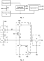
- Fig. 1 is a schematic structural diagram of a shift register according to an embodiment of the present disclosure.
- the shift register comprises an input circuit 10, a pull-up circuit 12, a pull-down circuit 13, a pulse width control circuit 11, and an output node OUT.
- An output terminal of the input circuit 10 is coupled to an input terminal of the pull-down circuit 13 and an input terminal of the pulse width control circuit 11 respectively.
- the pulse width control circuit 11 also has an output terminal coupled to an input terminal of the pull-up circuit 12, in addition to the pulse width control circuit 11 being coupled to the input circuit 10.
- the input circuit 10 comprises a trigger signal receiving terminal for receiving a trigger signal S, and is configured to control the pull-down circuit 13 to output a low level signal to the output node OUT based on a potential of the trigger signal S under control of a first control signal CK1 at a first control terminal.
- the pulse width control circuit 11 is configured to control the pull-up circuit 12 to output a high level signal to the output node OUT under control of the first control signal CK1 and a second control signal CK2 at a second control terminal, wherein a pulse width of the output high level signal varies with that of the trigger signal S received by the input circuit 10.
- a pulse width i.e., a width of a pulse
- a signal refers to a duration in which the signal is maintained at an active level.
- the pull-down circuit 13 is controlled to stop outputting the low level signal when the pull-up circuit 12 is controlled to output the high level signal, and the pull-up circuit 12 is controlled to stop outputting the high level signal when the pull-down circuit 13 is controlled to output the low level signal.
- a shift register which outputs a signal with a variable (adjustable) pulse width is realized in a simple manner. Since the shift register according to the embodiment of the present disclosure has a simpler structure than that of the shift register in the conventional art, a single stage of GOA may have a smaller layout area, which facilitates display with a narrow bezel.
- Fig. 2 is a circuit diagram of a shift register according to an embodiment of the present disclosure.
- the input circuit 10 receives the trigger signal STV via the trigger signal receiving terminal, and the output terminal of the input circuit 10 is coupled to a first node N1.
- the input circuit 10 is configured to control a potential at the first node N1 based on the potential of the trigger signal STV under control of the first control signal CK1.
- the first node N1 is coupled to the output terminal of the input circuit 10 and the input terminal of the pull-down circuit 13.
- the pull-down circuit 13 may output the low level signal to the output node OUT based on the potential at the first node N1.
- the input terminal of the pulse width control circuit 11 is coupled to the first node N1, and the output terminal of the pulse width control circuit 11 is coupled to a second node N2.
- the input terminal of the pull-up circuit 12 is also coupled to the second node N2.
- the pulse width control circuit 11 is configured to control a potential at the second node based on the potential at the first node under control of the first control signal CK1 and the second control signal CK2, so as to control the pull-up circuit 12 to output the high level signal to the output node OUT.
- the shift register is configured so that the pull-down circuit 13 is controlled by the first node N1 to stop outputting the low level signal when the pull-up circuit 12 is controlled by the second node N2 to output the high level signal.
- the first node N1 and the second node N2 are configured to operate in such a way, so that a timing at which the pull-up circuit and the pull-down circuit sequentially output the high level signal or the low level signal to the output node OUT is controlled.
- the pulse width control circuit 11 is further configured to, when the pull-up circuit 12 outputs the high level signal to the output node OUT, maintain the potential at the second node N2 to be a potential which enables the pull-up circuit 12 to output the high level signal to the output node OUT under control of the first control signal CK1 and the second control signal CK2.
- the pulse width control circuit 11 is further configured to operate in such a way, so that a duration in which the pull-up circuit is maintained to output the high level signal may be adjusted through the first control signal CK1 and the second control signal CK2, thereby realizing a shift register with an adjustable pulse width.
- the first control signal CK1 and the second control signal CK2 may be clock signals, which are set to be substantially inverted. Further, for the sake of simplicity, the circuit will be described by taking P-type transistors as an example.
- the input circuit 10 may comprise a first transistor T1 having a gate coupled to the first control terminal to receive the first control signal CK1, a first electrode coupled to a trigger signal terminal to receive the trigger signal STV, and a second electrode coupled to the first node N1.
- the first control signal CK1 is at an active level, for example, a low level in a case of a P-type transistor
- the first transistor T1 is turned on.
- the turn-on of the first transistor T1 causes the potential of the trigger signal STV to be transmitted to the first node N1.
- STV is at a high potential
- N1 is also at a high potential.
- the input terminal of the pull-down circuit 13 is also coupled to the first node N1, and whether the pull-down circuit 13 outputs the low level signal may be controlled by a high potential or a low potential at the first node N1.
- the pulse width control circuit 11 may comprise a second transistor T2, a third transistor T3, a fourth transistor T4, and a fifth transistor T5.
- the second transistor T2 has a gate coupled to the first node N1, a first electrode coupled to the second node N2, and a second electrode coupled to a first reference potential terminal, for example, a high potential terminal VGH.
- the third transistor T3 has a gate coupled to the first control terminal, a first electrode coupled to a second reference potential terminal, for example, a low potential terminal VGL, and a second electrode coupled to a third node N3.
- the fourth transistor T4 has a gate coupled to the third node N3, a first electrode coupled to the second reference potential terminal, for example, the low potential terminal VGL, and a second electrode coupled to a fourth node N4.
- the fifth transistor T5 has a gate coupled to the second control terminal, a first electrode coupled to the fourth node N4, and a second electrode coupled to the second node N2.
- the first transistor T1 is turned on to transmit the high potential of STV to the first node N1.
- the second transistor T2 is turned off.
- the low potential of CK1 also causes the third transistor T3 to be turned on, and a potential at the third node N3 is pulled down, so that the fourth transistor T4 is turned on to transmit the low potential VGL to the fourth node.
- the second control signal CK2 is at a low potential
- the low potential of CK2 causes the fifth transistor T5 to be turned on, to transmit the low potential at the fourth node to the second node N2.
- the potential at the second node N2 is pulled down, to control the pull-up circuit 12 to pull up a potential at the output node OUT to the high potential VGH.
- the pull-down circuit 13 may comprise a seventh transistor T7.
- a gate of the seventh transistor T7 is coupled to the first node N1, so that turn-on of the seventh transistor T7 is controlled by the potential at the first node N1.
- a first electrode of the seventh transistor T7 is coupled to the low potential terminal VGL, and a second electrode of the seventh transistor T7 is coupled to the output node OUT. Therefore, in a case of a P-type transistor, the seventh transistor T7 is turned on and the second electrode of the seventh transistor T7 outputs a low level signal when the first node N1 is at a low potential. When the first node N1 is at a high potential, the seventh transistor T7 is turned off, and the pull-down circuit 13 does not output a signal to the output node OUT.
- the pull-up circuit 12 may comprise an eighth transistor T8.
- the eighth transistor T8 has a gate coupled to the second node N2, a first electrode coupled to the high potential terminal VGH, and a second electrode coupled to the output node OUT.
- the pull-up circuit is coupled in such a way, so that whether the pull-up circuit 12 outputs the high level signal may be controlled by the potential at the second node N2.
- the eighth transistor T8 when the second node N2 is at a low potential, the eighth transistor T8 is turned on, and the pull-up circuit 12 outputs the high level signal at the high potential terminal VGH to OUT.
- a shift register with a simpler structure which enables a smaller layout area of a single stage of GOA, thus facilitating display with a narrow bezel.
- Fig. 3 is a circuit diagram of a shift register according to another embodiment of the present disclosure, wherein except that the pulse width control circuit 11, the pull-up circuit 12, and the pull-down circuit 13 comprise some additional components, remaining elements, signals or nodes referenced by the same numbers are the same as those in Fig. 2 .
- the pulse width control circuit 11 may further comprise a sixth transistor T6 and a first capacitor C1.
- the sixth transistor T6 has a gate coupled to the first node N1, a first electrode coupled to the first control terminal, and a second electrode coupled to the third node N3.
- the first capacitor C1 has one terminal coupled to the second control terminal CK2, and the other terminal coupled to the third node N3.
- the low potential of the second control signal CK2 may cause the fifth transistor T5 to be turned on, so that the second node N2 is pulled down.
- the high potential at N1 and the high potential of CK1 cause the third transistor T3 and the sixth transistor T6 to be in a turn-off state, so that the third node N3 is suspended, and thus may jump with the second control signal CK2, to enable the third node N3 to be pulled down better.
- the first node N1 may jump to a lower potential under action of a capacitor C2.
- T6 is still in a turn-on state, to transmit the high potential of CK1 to the third node N3.
- T4 may be turned off, to prevent the potential at the second node N2 from being pulled down due to turn-on of a connection between T5 and T4, thereby enabling the output node OUT to be maintained well in a state of outputting a low potential.
- the pull-down circuit 13 may further comprise a ninth transistor T9 and a second capacitor C2.
- the ninth transistor T9 has a gate coupled to the first node N1, a first electrode coupled to the second control signal CK2, and a second electrode coupled to one terminal of the second capacitor C2.
- the other terminal of the second capacitor C2 is coupled to the first node N1.
- the ninth transistor T9 is turned on, and a negative potential is stored by the second capacitor C2.
- the second control signal CK2 jumps to a low potential, the potential at the first node N1 is further pulled down.
- the ninth transistor T9 is configured so that the low level signal output by the pull-down circuit may not jitter due to the second capacitor C2, thus making the shift register circuit according to the present embodiment more stable.
- the pull-up circuit 12 may further comprise a third capacitor C3.
- the third capacitor C3 has one terminal coupled to the high potential terminal VGH, and the other terminal coupled to the gate of the eighth transistor T8.
- the third capacitor C3 may function to store and maintain a high potential when a high pulse is output.
- the shift register according to the embodiment shown in Fig. 3 may comprise transistors T1-T9 and three capacitors C1-C3, and related signals primarily comprise the first clock signal CK1, the second clock signal CK2, the trigger signal STV, the first reference potential signal VGH and the second reference potential signal VGL.
- the pull-up module may be controlled by the pulse width control module to output the high level signal under control of the first control signal and the second control signal, wherein a pulse width of the high level signal varies with that of the trigger signal.
- the shift register has a very simple structure, which is beneficial to reduce the layout area of the GOA, thereby achieving a narrow bezel design.
- Fig. 4 is a simulation timing diagram of a shift register according to an embodiment of the present disclosure. For convenience of description, the timing will be described in conjunction with the shift register according to the embodiment of the present disclosure shown in Fig. 3 .
- An operating process of the shift register may comprise four phases t1, t2, t3, t4, and t5.
- an operating principle of the shift register will be described as follows (transistors in this example are all P-type transistors).
- a first phase (a preliminary phase) t1 STV jumps to a high potential VGH, CK1 jumps to a low potential VGL, T1 is turned on to transmit the high potential of the STV signal to the first node N1, and at this time, T2, T6, T7 are turned off.
- the low potential of CK1 causes T3 to be turned on, and a potential at the third node N3 is pulled down.
- CK1 jumps to the high potential VGH
- CK2 jumps to the low potential VGL. Since T3 is turned on in the phase t1, the third node N3 is pulled to a low potential, and therefore a negative potential is stored by C1.
- the third node N3 may be pulled to a lower potential by a capacitor, and thereby T4 may be well turned on, so that the low potential of VGL may be transferred to the fourth node N4 without a threshold loss.
- the low potential of CK2 causes T5 to be turned on, and thereby the low potential at N4 causes the second node N2 to be pulled down, and T8 is turned on, so that the output node OUT is pulled up to the high potential VGH.
- a third phase (a high-potential maintenance phase) t3
- STV is still at a high potential in this phase.
- the operations in the phases t1 and t2 are repeated during the operating process of the circuit.
- a pull-down phase STV is at a low potential and CK1 jumps to a low potential.
- T1 is turned on, the first node N1 jumps to a low potential, T7 is turned on, and the potential at the output terminal OUT is pulled down.
- T9 is turned on, and a negative potential is stored by C2.
- CK2 jumps to a low potential, the first node N1 is further pulled down, which enhances a driving pull-down capability of T7.
- the output node OUT outputs a low potential without a threshold loss.
- a fifth phase (a low potential maintenance phase) t5
- STV is always at a low potential
- the operating process of t4 is repeated for CK1 and CK2, and the first node N1 and the second node N2 are maintained at a low potential and a high potential respectively, so that the output node OUT is well maintained at a low potential.
- the shift register according to the embodiment of the present disclosure at least has the following advantages.
- the structure is simple, a number of devices is small, and the control signal is simple.
- the output with different pulse widths of the GOA may be well realized by adjusting the pulse width of the trigger signal (i.e., controlling the duration of the active potential maintenance phase t3 of the shift register).
- each transistor is illustrated and described as a P-type transistor, an N-type transistor is also possible.
- a gate-on voltage is at a high potential
- a gate-off voltage is at a low potential.
- two reference potential terminals may be interchanged correspondingly, that is, the first reference potential is a low potential and the second reference potential is a high potential.
- the transistors may, for example, be thin film transistors, which are typically manufactured so that their first and second electrodes are used interchangeably. Other embodiments are also contemplated.
- the term "active potential” as used herein refers to a potential at which a circuit component (for example, a transistor) involved is enabled.
- the active potential is a high potential.
- the active potential is a low potential. It will be understood that the active potential or the inactive potential is not intended to refer to a specific potential, but may comprise a range of potentials.
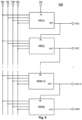
- Fig. 5 illustrates a gate driving circuit 500 according to an embodiment of the present disclosure, which comprises N cascaded shift registers SR(1), SR(2), ⁇ , SR(N-1) and SR(N) according to any of the embodiments described above, where N may be an integer greater than or equal to 2.
- N may be an integer greater than or equal to 2.
- an input terminal IN of each of the shift register circuits is coupled to an output terminal OUT of an adjacent previous shift register circuit.
- the gate driving circuit according to the embodiment of the present disclosure has an advantage of being simpler in structure and smaller in layout area.
- a display apparatus comprising the gate driving circuit according to the embodiment of the present disclosure.
- the display apparatus has the advantages of the gate driving circuit described above.
- the GOA has a simple structure, and a small layout area, and thereby may enable a narrow bezel design.
- the display apparatus may specifically comprise at least a liquid crystal display apparatus and an organic light emitting diode display apparatus.
- the display apparatus may be any product or component having a display function such as a liquid crystal display, a liquid crystal television, a digital photo frame, a mobile phone, or a tablet computer etc.
- the circuit described herein may be a TFT circuit or a MOS transistor circuit unless otherwise specified.
- the transistors mentioned herein may all be N-type transistors, in which case a high level signal is an active signal; or may all be P-type transistors, in which case a low level signal is an active signal.
- a first electrode of any of the transistors described above is a source, and a second electrode of the transistor is a drain; or the first electrode is a drain, and the second electrode is a source.
- the transistors described may be manufactured using an amorphous Silicon (a-Si) process, an oxide process, a Low Temperature Poly-Silicon (LTPS) process, a High Temperature Poly-Silicon (HTPS) process, etc.
- circuits may comprise circuit elements (for example, transistors, resistors, capacitors, inductors, etc.), integrated circuits, Application Specific Integrated Circuits (ASICs), Programmable Logic Devices (PLDs), Digital Signal Processors (DSPs), Field Programmable Gate Arrays (FPGAs), memory cells, logic gates, registers, semiconductor devices, etc.
- ASICs Application Specific Integrated Circuits
- PLDs Programmable Logic Devices
- DSPs Digital Signal Processors
- FPGAs Field Programmable Gate Arrays
- memory cells logic gates, registers, semiconductor devices, etc.
- first, second, third, etc. may be used herein to describe various elements, components and/or parts, these elements, components and/or parts should not be limited by these terms. These terms are only used to distinguish one element, component, or part from another element, component or part. Therefore, a first element, component or part discussed below may be referred to as a second element, component or part without departing from the teachings of the present disclosure.
Description
- The present disclosure relates to the field of display technology, and more particularly, to a shift register, a gate driving circuit, and a display device.
- In the display field, in order to continuously improve a display screen and enhance user experience, display with high definition, a high Pixels Per Inch (PPI), and a narrow bezel has become popular research. However, as a number of pixels increases, a number of rows required to be scanned by a shift register during one frame increases, which requires a smaller layout area and a simpler circuit structure of a single stage of Gate driver On Array (GOA). Therefore, how to design a GOA circuit with a simple structure is an urgent problem to be solved.
- Among GOA circuits (also known as gate driving circuits), there are a type of GOA circuits which are used to control a duration in which a pixel emits light. Such GOA circuits are called EMGOA circuits, which are usually implemented by using a shift register as a GOA unit circuit, wherein a width of a pulse output by the shift register determines a duration in which a pixel emits light. However, the shift register circuit in the related art has a relatively complicated structure, which results in a large layout area of a single stage of GOA, thus being disadvantageous for display with a narrow bezel.
- The US patent application
US 2016/133211 A1 discloses a shift register unit, gate drive circuit, and display device. The shift register unit comprises an input module, an NAND gate module, an inverter module, a pull-up module and a pull-down module. - The invention is defined by the appended claims.
- The above and other aspects of the present disclosure will now be described in more detail with reference to the accompanying drawings, which illustrate the embodiments of the present disclosure.
-
Fig. 1 is a schematic structural diagram of a shift register according to an embodiment of the present disclosure; -
Fig. 2 is a circuit diagram of a shift register according to an embodiment of the present disclosure; -
Fig. 3 is a circuit diagram of a shift register according to another embodiment of the present disclosure; -
Fig. 4 is a signal timing diagram of a shift register according to an embodiment of the present disclosure; and -
Fig. 5 is a schematic structural diagram of a gate driving circuit according to an embodiment of the present disclosure. - Various solutions and features of the present disclosure are described herein with reference to the accompanying drawings. These and other features of the present disclosure will become apparent from the following description of an alternative form of embodiments given as non-limiting examples with reference to the accompanying drawings. The specification may use phrases "in one embodiment", "in another embodiment", "in yet another embodiment" or "in other embodiments", which may all refer to one or more of the same or different embodiments according to the present disclosure. It is to be illustrated that, the same reference signs are used throughout specification to refer to the same or similar elements, and unnecessary repeated description is omitted. In addition, in the specific embodiments, elements which appear in a singular form do not exclude a condition of appearing in a multiple (plural) form.
-
Fig. 1 is a schematic structural diagram of a shift register according to an embodiment of the present disclosure. As shown inFig. 1 , the shift register comprises aninput circuit 10, a pull-up circuit 12, a pull-down circuit 13, a pulsewidth control circuit 11, and an output node OUT. An output terminal of theinput circuit 10 is coupled to an input terminal of the pull-down circuit 13 and an input terminal of the pulsewidth control circuit 11 respectively. The pulsewidth control circuit 11 also has an output terminal coupled to an input terminal of the pull-up circuit 12, in addition to the pulsewidth control circuit 11 being coupled to theinput circuit 10. - The
input circuit 10 comprises a trigger signal receiving terminal for receiving a trigger signal S, and is configured to control the pull-down circuit 13 to output a low level signal to the output node OUT based on a potential of the trigger signal S under control of a first control signal CK1 at a first control terminal. - The pulse
width control circuit 11 is configured to control the pull-up circuit 12 to output a high level signal to the output node OUT under control of the first control signal CK1 and a second control signal CK2 at a second control terminal, wherein a pulse width of the output high level signal varies with that of the trigger signal S received by theinput circuit 10. Herein, a pulse width (i.e., a width of a pulse) of a signal refers to a duration in which the signal is maintained at an active level. - In the shift register circuit, the pull-
down circuit 13 is controlled to stop outputting the low level signal when the pull-upcircuit 12 is controlled to output the high level signal, and the pull-up circuit 12 is controlled to stop outputting the high level signal when the pull-downcircuit 13 is controlled to output the low level signal. - Thereby, a shift register which outputs a signal with a variable (adjustable) pulse width is realized in a simple manner. Since the shift register according to the embodiment of the present disclosure has a simpler structure than that of the shift register in the conventional art, a single stage of GOA may have a smaller layout area, which facilitates display with a narrow bezel.
-
Fig. 2 is a circuit diagram of a shift register according to an embodiment of the present disclosure. - The
input circuit 10 receives the trigger signal STV via the trigger signal receiving terminal, and the output terminal of theinput circuit 10 is coupled to a first node N1. Theinput circuit 10 is configured to control a potential at the first node N1 based on the potential of the trigger signal STV under control of the first control signal CK1. The first node N1 is coupled to the output terminal of theinput circuit 10 and the input terminal of the pull-down circuit 13. The pull-down circuit 13 may output the low level signal to the output node OUT based on the potential at the first node N1. - The input terminal of the pulse
width control circuit 11 is coupled to the first node N1, and the output terminal of the pulsewidth control circuit 11 is coupled to a second node N2. The input terminal of the pull-up circuit 12 is also coupled to the second node N2. The pulsewidth control circuit 11 is configured to control a potential at the second node based on the potential at the first node under control of the first control signal CK1 and the second control signal CK2, so as to control the pull-up circuit 12 to output the high level signal to the output node OUT. Further, the shift register is configured so that the pull-down circuit 13 is controlled by the first node N1 to stop outputting the low level signal when the pull-upcircuit 12 is controlled by the second node N2 to output the high level signal. - The first node N1 and the second node N2 are configured to operate in such a way, so that a timing at which the pull-up circuit and the pull-down circuit sequentially output the high level signal or the low level signal to the output node OUT is controlled.
- In an embodiment, the pulse
width control circuit 11 is further configured to, when the pull-up circuit 12 outputs the high level signal to the output node OUT, maintain the potential at the second node N2 to be a potential which enables the pull-up circuit 12 to output the high level signal to the output node OUT under control of the first control signal CK1 and the second control signal CK2. - Thereby, in this embodiment, the pulse
width control circuit 11 is further configured to operate in such a way, so that a duration in which the pull-up circuit is maintained to output the high level signal may be adjusted through the first control signal CK1 and the second control signal CK2, thereby realizing a shift register with an adjustable pulse width. - An exemplary circuit structure of the shift register according to the embodiment of the present disclosure will be described in detail below with reference to
Fig. 2 . In the following description, the first control signal CK1 and the second control signal CK2 may be clock signals, which are set to be substantially inverted. Further, for the sake of simplicity, the circuit will be described by taking P-type transistors as an example. - The
input circuit 10 may comprise a first transistor T1 having a gate coupled to the first control terminal to receive the first control signal CK1, a first electrode coupled to a trigger signal terminal to receive the trigger signal STV, and a second electrode coupled to the first node N1. When the first control signal CK1 is at an active level, for example, a low level in a case of a P-type transistor, the first transistor T1 is turned on. The turn-on of the first transistor T1 causes the potential of the trigger signal STV to be transmitted to the first node N1. For example, if STV is at a high potential, N1 is also at a high potential. The input terminal of the pull-down circuit 13 is also coupled to the first node N1, and whether the pull-down circuit 13 outputs the low level signal may be controlled by a high potential or a low potential at the first node N1. - The pulse
width control circuit 11 may comprise a second transistor T2, a third transistor T3, a fourth transistor T4, and a fifth transistor T5. The second transistor T2 has a gate coupled to the first node N1, a first electrode coupled to the second node N2, and a second electrode coupled to a first reference potential terminal, for example, a high potential terminal VGH. The third transistor T3 has a gate coupled to the first control terminal, a first electrode coupled to a second reference potential terminal, for example, a low potential terminal VGL, and a second electrode coupled to a third node N3. The fourth transistor T4 has a gate coupled to the third node N3, a first electrode coupled to the second reference potential terminal, for example, the low potential terminal VGL, and a second electrode coupled to a fourth node N4. The fifth transistor T5 has a gate coupled to the second control terminal, a first electrode coupled to the fourth node N4, and a second electrode coupled to the second node N2. - For the
input circuit 10 and the pulsewidth control circuit 11 having the above structures, in a preliminary phase, when the trigger signal STV jumps to a high potential VGH, and the first control signal CK1 jumps to a low potential VGL, the first transistor T1 is turned on to transmit the high potential of STV to the first node N1. When N1 is at a high potential, the second transistor T2 is turned off. The low potential of CK1 also causes the third transistor T3 to be turned on, and a potential at the third node N3 is pulled down, so that the fourth transistor T4 is turned on to transmit the low potential VGL to the fourth node. At this time, if the second control signal CK2 is at a low potential, the low potential of CK2 causes the fifth transistor T5 to be turned on, to transmit the low potential at the fourth node to the second node N2. In this way, the potential at the second node N2 is pulled down, to control the pull-upcircuit 12 to pull up a potential at the output node OUT to the high potential VGH. - The pull-
down circuit 13 may comprise a seventh transistor T7. A gate of the seventh transistor T7 is coupled to the first node N1, so that turn-on of the seventh transistor T7 is controlled by the potential at the first node N1. A first electrode of the seventh transistor T7 is coupled to the low potential terminal VGL, and a second electrode of the seventh transistor T7 is coupled to the output node OUT. Therefore, in a case of a P-type transistor, the seventh transistor T7 is turned on and the second electrode of the seventh transistor T7 outputs a low level signal when the first node N1 is at a low potential. When the first node N1 is at a high potential, the seventh transistor T7 is turned off, and the pull-down circuit 13 does not output a signal to the output node OUT. - The pull-up
circuit 12 may comprise an eighth transistor T8. The eighth transistor T8 has a gate coupled to the second node N2, a first electrode coupled to the high potential terminal VGH, and a second electrode coupled to the output node OUT. - The pull-up circuit is coupled in such a way, so that whether the pull-up
circuit 12 outputs the high level signal may be controlled by the potential at the second node N2. For example, in an example of a P-type transistor, when the second node N2 is at a low potential, the eighth transistor T8 is turned on, and the pull-upcircuit 12 outputs the high level signal at the high potential terminal VGH to OUT. - According to an embodiment of the present disclosure, there is provided a shift register with a simpler structure, which enables a smaller layout area of a single stage of GOA, thus facilitating display with a narrow bezel.
-
Fig. 3 is a circuit diagram of a shift register according to another embodiment of the present disclosure, wherein except that the pulsewidth control circuit 11, the pull-upcircuit 12, and the pull-down circuit 13 comprise some additional components, remaining elements, signals or nodes referenced by the same numbers are the same as those inFig. 2 . - As shown in
Fig. 3 , in an embodiment, additionally, the pulsewidth control circuit 11 may further comprise a sixth transistor T6 and a first capacitor C1. The sixth transistor T6 has a gate coupled to the first node N1, a first electrode coupled to the first control terminal, and a second electrode coupled to the third node N3. The first capacitor C1 has one terminal coupled to the second control terminal CK2, and the other terminal coupled to the third node N3. - Thus, in a case where STV is at a high potential, when the second control signal CK2 jumps to the high potential VGL and the first control signal CK1 jumps to the high potential VGH, since the third transistor T3 has been turned on, the third node N3 is pulled down to a low potential, and therefore a negative potential is stored by the first capacitor C1. Thus, when the second control signal CK2 jumps to a low potential, the third node N3 may be pulled down to a lower potential by the capacitor, so that the fourth transistor T4 may be turned on well, and thereby the low potential at the low potential terminal VGL is transmitted to the fourth node N4, that is, the first electrode of the fifth transistor, without a threshold loss. The low potential of the second control signal CK2 may cause the fifth transistor T5 to be turned on, so that the second node N2 is pulled down. In this phase, the high potential at N1 and the high potential of CK1 cause the third transistor T3 and the sixth transistor T6 to be in a turn-off state, so that the third node N3 is suspended, and thus may jump with the second control signal CK2, to enable the third node N3 to be pulled down better.
- In a phase in which the potential at the output node OUT is pulled down and outputs a low potential, when CK1 jumps to a high potential and CK2 jumps to a low potential, the first node N1 may jump to a lower potential under action of a capacitor C2. At this time, T6 is still in a turn-on state, to transmit the high potential of CK1 to the third node N3. In this way, T4 may be turned off, to prevent the potential at the second node N2 from being pulled down due to turn-on of a connection between T5 and T4, thereby enabling the output node OUT to be maintained well in a state of outputting a low potential.
- In an embodiment, additionally, the pull-
down circuit 13 may further comprise a ninth transistor T9 and a second capacitor C2. The ninth transistor T9 has a gate coupled to the first node N1, a first electrode coupled to the second control signal CK2, and a second electrode coupled to one terminal of the second capacitor C2. The other terminal of the second capacitor C2 is coupled to the first node N1. - For the pull-
down circuit 13 with such a structure, after the first node N1 jumps to the potential, the ninth transistor T9 is turned on, and a negative potential is stored by the second capacitor C2. When the second control signal CK2 jumps to a low potential, the potential at the first node N1 is further pulled down. - In this way, a driving pull-down capability of the seventh transistor T7 is enhanced. The output node OUT may even output a low potential without a threshold loss. Further, the ninth transistor T9 is configured so that the low level signal output by the pull-down circuit may not jitter due to the second capacitor C2, thus making the shift register circuit according to the present embodiment more stable.
- In an embodiment, additionally, the pull-up
circuit 12 may further comprise a third capacitor C3. The third capacitor C3 has one terminal coupled to the high potential terminal VGH, and the other terminal coupled to the gate of the eighth transistor T8. The third capacitor C3 may function to store and maintain a high potential when a high pulse is output. - The shift register according to the embodiment shown in
Fig. 3 may comprise transistors T1-T9 and three capacitors C1-C3, and related signals primarily comprise the first clock signal CK1, the second clock signal CK2, the trigger signal STV, the first reference potential signal VGH and the second reference potential signal VGL. - In the shift register according to the embodiment of the present disclosure, the pull-up module may be controlled by the pulse width control module to output the high level signal under control of the first control signal and the second control signal, wherein a pulse width of the high level signal varies with that of the trigger signal. The shift register has a very simple structure, which is beneficial to reduce the layout area of the GOA, thereby achieving a narrow bezel design.
-
Fig. 4 is a simulation timing diagram of a shift register according to an embodiment of the present disclosure. For convenience of description, the timing will be described in conjunction with the shift register according to the embodiment of the present disclosure shown inFig. 3 . An operating process of the shift register may comprise four phases t1, t2, t3, t4, and t5. As shown inFig. 4 , an operating principle of the shift register will be described as follows (transistors in this example are all P-type transistors). - In a first phase (a preliminary phase) t1, STV jumps to a high potential VGH, CK1 jumps to a low potential VGL, T1 is turned on to transmit the high potential of the STV signal to the first node N1, and at this time, T2, T6, T7 are turned off. At the same time, the low potential of CK1 causes T3 to be turned on, and a potential at the third node N3 is pulled down.
- In a second phase (a pull-up phase) t2, CK1 jumps to the high potential VGH, and CK2 jumps to the low potential VGL. Since T3 is turned on in the phase t1, the third node N3 is pulled to a low potential, and therefore a negative potential is stored by C1. When CK2 jumps to a low potential, the third node N3 may be pulled to a lower potential by a capacitor, and thereby T4 may be well turned on, so that the low potential of VGL may be transferred to the fourth node N4 without a threshold loss. The low potential of CK2 causes T5 to be turned on, and thereby the low potential at N4 causes the second node N2 to be pulled down, and T8 is turned on, so that the output node OUT is pulled up to the high potential VGH.
- In a third phase (a high-potential maintenance phase) t3, STV is still at a high potential in this phase. In the high potential-to-low potential/low potential-tohigh potential jump process of CK1 and CK2, as long as the STV is not at a low potential at the same time as CK1, the operations in the phases t1 and t2 are repeated during the operating process of the circuit.
- In a fourth phase (a pull-down phase) t4, STV is at a low potential and CK1 jumps to a low potential. At this time, T1 is turned on, the first node N1 jumps to a low potential, T7 is turned on, and the potential at the output terminal OUT is pulled down. After the first node N1 jumps to a low potential, T9 is turned on, and a negative potential is stored by C2. When CK2 jumps to a low potential, the first node N1 is further pulled down, which enhances a driving pull-down capability of T7. The output node OUT outputs a low potential without a threshold loss. Since the output node OUT changes to output a low potential under control of CK1 only after STV changes from an active potential to an inactive potential, for example, from a high potential to a low potential, a pulse width of the output node OUT varies with that of STV.
- In a fifth phase (a low potential maintenance phase) t5, STV is always at a low potential, the operating process of t4 is repeated for CK1 and CK2, and the first node N1 and the second node N2 are maintained at a low potential and a high potential respectively, so that the output node OUT is well maintained at a low potential.
- The shift register according to the embodiment of the present disclosure at least has the following advantages.
- The structure is simple, a number of devices is small, and the control signal is simple.
- In addition, the output with different pulse widths of the GOA may be well realized by adjusting the pulse width of the trigger signal (i.e., controlling the duration of the active potential maintenance phase t3 of the shift register).
- As can be appreciated, in the embodiments of
Figs. 2 ,3 , and4 , although each transistor is illustrated and described as a P-type transistor, an N-type transistor is also possible. In a case of an N-type transistor, a gate-on voltage is at a high potential, and a gate-off voltage is at a low potential. At this time, compared with a solution using a P-type transistor, two reference potential terminals may be interchanged correspondingly, that is, the first reference potential is a low potential and the second reference potential is a high potential. In various embodiments, the transistors may, for example, be thin film transistors, which are typically manufactured so that their first and second electrodes are used interchangeably. Other embodiments are also contemplated. - As can be appreciated, the term "active potential" as used herein refers to a potential at which a circuit component (for example, a transistor) involved is enabled. For an N-type transistor, the active potential is a high potential. For a P-type transistor, the active potential is a low potential. It will be understood that the active potential or the inactive potential is not intended to refer to a specific potential, but may comprise a range of potentials.
-
Fig. 5 illustrates agate driving circuit 500 according to an embodiment of the present disclosure, which comprises N cascaded shift registers SR(1), SR(2), ···, SR(N-1) and SR(N) according to any of the embodiments described above, where N may be an integer greater than or equal to 2. In thegate driver 500, except for a first shift register circuit SR(1), an input terminal IN of each of the shift register circuits is coupled to an output terminal OUT of an adjacent previous shift register circuit. For example, an input terminal IN of SR(n) is coupled to an output terminal OUT of SR(n-1), where 1 <n<=N. - The gate driving circuit according to the embodiment of the present disclosure has an advantage of being simpler in structure and smaller in layout area.
- In still another embodiment, there is provided a display apparatus, comprising the gate driving circuit according to the embodiment of the present disclosure.
- Therefore, the display apparatus according to the present embodiment has the advantages of the gate driving circuit described above. For example, the GOA has a simple structure, and a small layout area, and thereby may enable a narrow bezel design.
- The display apparatus may specifically comprise at least a liquid crystal display apparatus and an organic light emitting diode display apparatus. For example, the display apparatus may be any product or component having a display function such as a liquid crystal display, a liquid crystal television, a digital photo frame, a mobile phone, or a tablet computer etc.
- The circuit described herein may be a TFT circuit or a MOS transistor circuit unless otherwise specified. The transistors mentioned herein may all be N-type transistors, in which case a high level signal is an active signal; or may all be P-type transistors, in which case a low level signal is an active signal. In addition, a first electrode of any of the transistors described above is a source, and a second electrode of the transistor is a drain; or the first electrode is a drain, and the second electrode is a source. The transistors described may be manufactured using an amorphous Silicon (a-Si) process, an oxide process, a Low Temperature Poly-Silicon (LTPS) process, a High Temperature Poly-Silicon (HTPS) process, etc.
- Various embodiments may be implemented using circuits. Examples of the circuits may comprise circuit elements (for example, transistors, resistors, capacitors, inductors, etc.), integrated circuits, Application Specific Integrated Circuits (ASICs), Programmable Logic Devices (PLDs), Digital Signal Processors (DSPs), Field Programmable Gate Arrays (FPGAs), memory cells, logic gates, registers, semiconductor devices, etc.
- It will be understood that, although the terms first, second, third, etc. may be used herein to describe various elements, components and/or parts, these elements, components and/or parts should not be limited by these terms. These terms are only used to distinguish one element, component, or part from another element, component or part. Therefore, a first element, component or part discussed below may be referred to as a second element, component or part without departing from the teachings of the present disclosure.
- The terms used herein is for the purpose of describing particular embodiments and is not intended to limit the present disclosure. As used herein, singular forms "a", "an", and "the" are intended to comprise plural forms unless the context clearly indicates otherwise. It will be further understood that the terms "comprise" and/or "contain", when used in the specification, are intended to refer to the presence of the features, integers, steps, operations, elements and/or components, but should not preclude the presence or addition of one or more other features, integers, steps, operations, elements, components, and/or groups thereof. As used herein, the term "and/or" comprises any and all combinations of one or more of associated listed items.
- It will be understood that when an element is referred to as "connected to another element" or "coupled to another element", it may be directly connected to the other element or directly coupled to the other element, or there may be an intermediate element therebetween. In contrast, when an element is referred to as "directly connected to another element" or "directly coupled to another element," there is no intermediate element therebetween.
- All terms (comprising technical and scientific terms) used here have the same meaning as commonly understood by those of ordinary skill in the art to which the present disclosure belongs, unless otherwise defined. It should also be understood that terms such as those defined in a general dictionary should be understood to have meaning consistent with the meaning in the context of the related art and/or the present specification, and will not be explained as an idealized or excessively formal meaning unless specifically defined as here.
Claims (11)
- A shift register comprising an input circuit (10), a pull-up circuit (12), a pulldown circuit (13), a pulse width control circuit (11), and an output node (OUT), whereinthe input circuit (10) comprises a trigger signal receiving terminal for receiving a trigger signal (S, STV), and is configured to control the pull-down circuit (13) to output a low level signal to the output node (OUT) based on the trigger signal (S, STV) under control of a first control signal (CK1) at a first control terminal; andthe pulse width control circuit (11) is configured to control the pull-up circuit (12) to output a high level signal to the output node (OUT) under control of the first control signal (CK1) and a second control signal (CK2) at a second control terminal, wherein a pulse width of the high level signal varies with a pulse width of the trigger signal (S, STV),wherein when the pull-up circuit (12) is controlled to output the high level signal, the pull-down circuit (13) is controlled to stop outputting the low level signal, and when the pull-down circuit (13) is controlled to output the low level signal, the pull-up circuit (12) is controlled to stop outputting the high level signal,an output terminal of the input circuit (10) and an input terminal of the pulse width control circuit (11) are coupled to a first node (N1),an output terminal of the pulse width control circuit (11) and an input terminal of the pull-up circuit (12) are coupled to a second node (N2),wherein the input circuit (10) is further configured to control a potential at the first node (N1) based on the trigger signal (S, STV) under control of the first control signal (CK1), andthe pulse width control circuit (11) is further configured to:control the pull-up circuit (12) to output the high level signal by controlling a potential at the second node (N2) using the potential at the first node (N1) under control of the first control signal (CK1) and the second control signal (CK2), andthe pull-down circuit (13) is controlled by the potential at the first node (N1) to stop outputting the low level signal when the pull-up circuit (12) is controlled by the potential at the second node (N2) to output the high level signal,wherein the pulse width control circuit (11) comprises a second transistor (T2), a third transistor (T3), a fourth transistor (T4), and a fifth transistor (T5), characterized bythe second transistor (T2) has a gate electrically coupled to the first node (N1), a first electrode electrically coupled to the second node (N2), and a second electrode electrically coupled to a first reference potential terminal,the third transistor (T3) has a gate electrically coupled to the first control terminal, and a first electrode electrically coupled to a low potential terminal (VGL),the fourth transistor (T4) has a gate electrically coupled to a second electrode of the third transistor (T3), and a first electrode electrically coupled to a second reference potential terminal, andthe fifth transistor (T5) has a gate electrically coupled to the second control terminal, a first electrode electrically coupled to a second electrode of the fourth transistor (T4), and a second electrode electrically coupled to the first electrode of the second transistor (T2).
- The shift register according to claim 1, wherein
the pulse width control circuit (11) is further configured to, when the pull-up circuit (12) outputs the high level signal to the output node (OUT), maintain the potential at the second node (N2) to be a potential which enables the pull-up circuit (12) to output the high level signal to the output node (OUT) under control of the first control signal (CK1) and the second control signal (CK2). - The shift register according to claim 2, wherein the input circuit (10) comprises a first transistor (T1) having a gate electrically coupled to the first control signal (CK1), a first electrode electrically coupled to receive the trigger signal (S, STV), and a second electrode electrically coupled to the first node (N1), and configured to transmit a potential of the trigger signal (S, STV) to the first node (N1) when the first transistor (T1) is turned on under control of the first control signal (CK1)..
- The shift register according to claim 1, wherein the pulse width control circuit (11) further comprises a sixth transistor (T6) and a first capacitor (C1), whereinthe sixth transistor (T6) has a gate electrically coupled to the first node (N1), a first electrode electrically coupled to the first control terminal, and a second electrode electrically coupled to the gate of the fourth transistor (T4), andthe first capacitor (C1) has one terminal coupled to the second control terminal, and the other terminal coupled to the gate of the fourth transistor (T4).
- The shift register according to any of claims 1 to 4, wherein
the pull-down circuit (13) comprises a seventh transistor (T7) having a gate electrically coupled to the first node (N1), a first electrode electrically coupled to the low potential terminal (VGL), and a second electrode electrically coupled to the output node (OUT). - The shift register according to any of claims 1 to 5, wherein the pull-up circuit (12) comprises an eighth transistor (T8) having a gate electrically coupled to the second node (N2), a first electrode electrically coupled to a high potential terminal (VGH), and a second electrode electrically coupled to the output node (OUT).
- The shift register according to claim 5, wherein the pull-down circuit (13) further comprises a ninth transistor (T9) and a second capacitor (C2), whereinthe ninth transistor (T9) has a gate electrically coupled to the first node (N1), a first electrode electrically coupled to the second control terminal, and a second electrode electrically coupled to one terminal of the second capacitor (C2), andthe other terminal of the second capacitor (C2) is electrically coupled to the first node (N1).
- The shift register according to claim 6, wherein
the pull-up circuit (12) further comprises a third capacitor (C3) having one terminal coupled to the high potential terminal (VGH), and the other terminal coupled to the gate of the eighth transistor (T8). - A gate driving circuit comprising the shift register according to any of claims 1 to 8.
- A display device comprising the gate driving circuit according to claim 9.
- The shift register according to claim 1, wherein the first reference potential and the second reference potential are opposite potentials.
Applications Claiming Priority (2)
| Application Number | Priority Date | Filing Date | Title |
|---|---|---|---|
| CN201810164919.2A CN110197697B (en) | 2018-02-24 | 2018-02-24 | Shift register, gate drive circuit and display device |
| PCT/CN2018/112575 WO2019161676A1 (en) | 2018-02-24 | 2018-10-30 | Shift register, gate driver on array circuit and display device |
Publications (3)
| Publication Number | Publication Date |
|---|---|
| EP3758002A1 EP3758002A1 (en) | 2020-12-30 |
| EP3758002A4 EP3758002A4 (en) | 2021-10-06 |
| EP3758002B1 true EP3758002B1 (en) | 2024-01-10 |
Family
ID=67687912
Family Applications (1)
| Application Number | Title | Priority Date | Filing Date |
|---|---|---|---|
| EP18906812.5A Active EP3758002B1 (en) | 2018-02-24 | 2018-10-30 | Shift register, gate driver on array circuit and display device |
Country Status (6)
| Country | Link |
|---|---|
| US (1) | US10885826B2 (en) |
| EP (1) | EP3758002B1 (en) |
| JP (1) | JP2021515252A (en) |
| KR (1) | KR102343268B1 (en) |
| CN (1) | CN110197697B (en) |
| WO (1) | WO2019161676A1 (en) |
Families Citing this family (5)
| Publication number | Priority date | Publication date | Assignee | Title |
|---|---|---|---|---|
| CN107154234B (en) * | 2017-07-20 | 2020-01-21 | 京东方科技集团股份有限公司 | Shifting register unit, driving method, grid driving circuit and display device |
| CN111508433B (en) | 2020-05-28 | 2021-08-31 | 京东方科技集团股份有限公司 | Signal generation circuit, signal generation method, signal generation module and display device |
| CN112802422B (en) * | 2021-01-29 | 2022-06-10 | 云谷(固安)科技有限公司 | Shift register, grid drive circuit and display panel |
| CN113628576B (en) * | 2021-08-17 | 2023-06-02 | 深圳市华星光电半导体显示技术有限公司 | Driving circuit |
| CN116913200B (en) * | 2023-09-07 | 2023-12-01 | 上海视涯技术有限公司 | Shifting register circuit, silicon-based display panel and display device |
Family Cites Families (15)
| Publication number | Priority date | Publication date | Assignee | Title |
|---|---|---|---|---|
| KR100789153B1 (en) | 2002-03-06 | 2007-12-28 | 삼성전자주식회사 | Shift register and liquid crystal display with the same |
| KR101975581B1 (en) * | 2012-08-21 | 2019-09-11 | 삼성디스플레이 주식회사 | Emission driver and organic light emitting display deivce including the same |
| KR101997775B1 (en) | 2012-12-05 | 2019-10-01 | 엘지디스플레이 주식회사 | Shift register and flat panel display device including the same |
| CN104282288B (en) | 2014-11-07 | 2016-08-17 | 京东方科技集团股份有限公司 | Shift register cell and use its gate driver circuit and display device |
| CN104795034B (en) | 2015-04-17 | 2018-01-30 | 深圳市华星光电技术有限公司 | A kind of GOA circuits and liquid crystal display |
| CN104809978B (en) * | 2015-05-21 | 2017-05-17 | 京东方科技集团股份有限公司 | Shifting register unit, driving method of shifting register unit, grid driving circuit and display device |
| CN104835450B (en) * | 2015-05-22 | 2017-01-25 | 京东方科技集团股份有限公司 | Shift register unit, control method therefor, grid drive circuit, and display device |
| CN105096808B (en) * | 2015-09-18 | 2018-02-16 | 京东方科技集团股份有限公司 | Shift register cell and its driving method, gate driving circuit and display device |
| CN105206243B (en) * | 2015-10-28 | 2017-10-17 | 京东方科技集团股份有限公司 | A kind of shift register, grid integrated drive electronics and display device |
| CN105513531B (en) * | 2016-03-02 | 2018-04-10 | 京东方科技集团股份有限公司 | Shift register cell, driving method, gate driving circuit and display device |
| CN105609041B (en) * | 2016-03-23 | 2018-08-07 | 京东方科技集团股份有限公司 | Shift register cell and its driving method, gate driving circuit, display device |
| CN105741802B (en) * | 2016-03-28 | 2018-01-30 | 京东方科技集团股份有限公司 | Shift register cell and its driving method, gate driving circuit, display device |
| KR102511947B1 (en) * | 2016-06-17 | 2023-03-21 | 삼성디스플레이 주식회사 | Stage and Organic Light Emitting Display Device Using the same |
| CN106782406B (en) * | 2017-02-08 | 2019-04-09 | 京东方科技集团股份有限公司 | Shift-register circuit and its driving method, gate driving circuit, display panel |
| CN107424649B (en) * | 2017-05-25 | 2020-09-18 | 上海天马有机发光显示技术有限公司 | Shift register, driving method thereof, light-emitting control circuit and display device |
-
2018
- 2018-02-24 CN CN201810164919.2A patent/CN110197697B/en active Active
- 2018-10-30 WO PCT/CN2018/112575 patent/WO2019161676A1/en active Application Filing
- 2018-10-30 EP EP18906812.5A patent/EP3758002B1/en active Active
- 2018-10-30 JP JP2019560280A patent/JP2021515252A/en active Pending
- 2018-10-30 KR KR1020197033285A patent/KR102343268B1/en active IP Right Grant
- 2018-10-30 US US16/610,282 patent/US10885826B2/en active Active
Also Published As
| Publication number | Publication date |
|---|---|
| EP3758002A4 (en) | 2021-10-06 |
| KR102343268B1 (en) | 2021-12-27 |
| KR20190131596A (en) | 2019-11-26 |
| US10885826B2 (en) | 2021-01-05 |
| CN110197697B (en) | 2021-02-26 |
| US20200143730A1 (en) | 2020-05-07 |
| CN110197697A (en) | 2019-09-03 |
| JP2021515252A (en) | 2021-06-17 |
| WO2019161676A1 (en) | 2019-08-29 |
| EP3758002A1 (en) | 2020-12-30 |
Similar Documents
| Publication | Publication Date | Title |
|---|---|---|
| US10902931B2 (en) | Shift register unit and method for driving the same, gate driving circuit, and display apparatus | |
| EP3758002B1 (en) | Shift register, gate driver on array circuit and display device | |
| US9640276B2 (en) | Shift register unit and gate driving circuit | |
| US10984879B2 (en) | Shift register unit and method for driving the same, gate driving circuit and display apparatus | |
| US9965985B2 (en) | Shift register and method for driving the same, gate driving circuit and display apparatus | |
| EP3223268B1 (en) | Shift register unit and driving method therefor, shift register, and display device | |
| US11011089B2 (en) | Shift register unit and method for driving the same, gate driving circuit, array substrate and display apparatus | |
| US10593416B2 (en) | Shift register, driving method, gate driving circuit and display device | |
| US11282470B2 (en) | Shift register element, method for driving the same, gate driver circuit, and display device | |
| US20170287428A1 (en) | Gate driving circuit and method of driving the same, display panel | |
| US10657879B1 (en) | Gate driving circuit, method for driving the same, and display apparatus | |
| US20190279588A1 (en) | Shift register unit, gate driving circuit, display and gate driving method | |
| US8532248B2 (en) | Shift register unit circuit, shift register, array substrate and liquid crystal display | |
| EP3365895B1 (en) | Shift register unit, method for driving the same, related gate driver circuit, and related semiconductor device | |
| CN107516505B (en) | Shifting register unit and driving method thereof, grid driving circuit and display panel | |
| US20190295674A1 (en) | Shift Register Unit and Driving Method Thereof, Gate Driving Circuit, and Display Device | |
| US11183103B2 (en) | Shift register unit and driving method thereof, gate driving circuit, and display device | |
| US10872546B2 (en) | Shift register unit and method for driving the same, gate driving circuit and display apparatus | |
| US10818259B2 (en) | Scanning trigger unit, gate driving circuit and method for driving the same and display apparatus | |
| US10930189B2 (en) | Shift register unit, method for driving the same, gate driving circuit and display device | |
| KR102098133B1 (en) | Shift register circuit, XOA circuit, and display device and driving method thereof | |
| US20210272506A1 (en) | Shift register and driving method thereof, gate driving circuit and display device | |
| CN106683617B (en) | Shifting register unit, array substrate and display device | |
| US11227525B2 (en) | Shift register unit and method for driving the same, gate driving circuit and method for driving the same, and display apparatus |
Legal Events
| Date | Code | Title | Description |
|---|---|---|---|
| STAA | Information on the status of an ep patent application or granted ep patent |
Free format text: STATUS: THE INTERNATIONAL PUBLICATION HAS BEEN MADE |
|
| PUAI | Public reference made under article 153(3) epc to a published international application that has entered the european phase |
Free format text: ORIGINAL CODE: 0009012 |
|
| STAA | Information on the status of an ep patent application or granted ep patent |
Free format text: STATUS: REQUEST FOR EXAMINATION WAS MADE |
|
| 17P | Request for examination filed |
Effective date: 20200116 |
|
| AK | Designated contracting states |
Kind code of ref document: A1 Designated state(s): AL AT BE BG CH CY CZ DE DK EE ES FI FR GB GR HR HU IE IS IT LI LT LU LV MC MK MT NL NO PL PT RO RS SE SI SK SM TR |
|
| AX | Request for extension of the european patent |
Extension state: BA ME |
|
| DAV | Request for validation of the european patent (deleted) | ||
| DAX | Request for extension of the european patent (deleted) | ||
| A4 | Supplementary search report drawn up and despatched |
Effective date: 20210902 |
|
| RIC1 | Information provided on ipc code assigned before grant |
Ipc: G02F 1/1345 20060101ALI20210827BHEP Ipc: G09G 3/3208 20160101ALI20210827BHEP Ipc: G09G 3/36 20060101ALI20210827BHEP Ipc: G11C 19/28 20060101AFI20210827BHEP |
|
| P01 | Opt-out of the competence of the unified patent court (upc) registered |
Effective date: 20230630 |
|
| GRAP | Despatch of communication of intention to grant a patent |
Free format text: ORIGINAL CODE: EPIDOSNIGR1 |
|
| STAA | Information on the status of an ep patent application or granted ep patent |
Free format text: STATUS: GRANT OF PATENT IS INTENDED |
|
| INTG | Intention to grant announced |
Effective date: 20230918 |
|
| GRAS | Grant fee paid |
Free format text: ORIGINAL CODE: EPIDOSNIGR3 |
|
| GRAA | (expected) grant |
Free format text: ORIGINAL CODE: 0009210 |
|
| STAA | Information on the status of an ep patent application or granted ep patent |
Free format text: STATUS: THE PATENT HAS BEEN GRANTED |
|
| AK | Designated contracting states |
Kind code of ref document: B1 Designated state(s): AL AT BE BG CH CY CZ DE DK EE ES FI FR GB GR HR HU IE IS IT LI LT LU LV MC MK MT NL NO PL PT RO RS SE SI SK SM TR |
|
| REG | Reference to a national code |
Ref country code: GB Ref legal event code: FG4D |
|
| REG | Reference to a national code |
Ref country code: CH Ref legal event code: EP |
|
| REG | Reference to a national code |
Ref country code: DE Ref legal event code: R096 Ref document number: 602018064127 Country of ref document: DE |
|
| REG | Reference to a national code |
Ref country code: IE Ref legal event code: FG4D |