EP3757748A1 - Datenspeichervorrichtung zur erfassung der versorgungsstromgrenze - Google Patents
Datenspeichervorrichtung zur erfassung der versorgungsstromgrenze Download PDFInfo
- Publication number
- EP3757748A1 EP3757748A1 EP20161100.1A EP20161100A EP3757748A1 EP 3757748 A1 EP3757748 A1 EP 3757748A1 EP 20161100 A EP20161100 A EP 20161100A EP 3757748 A1 EP3757748 A1 EP 3757748A1
- Authority
- EP
- European Patent Office
- Prior art keywords
- load
- data storage
- storage device
- detected
- current limit
- Prior art date
- Legal status (The legal status is an assumption and is not a legal conclusion. Google has not performed a legal analysis and makes no representation as to the accuracy of the status listed.)
- Granted
Links
Images


Classifications
-
- G—PHYSICS
- G06—COMPUTING OR CALCULATING; COUNTING
- G06F—ELECTRIC DIGITAL DATA PROCESSING
- G06F1/00—Details not covered by groups G06F3/00 - G06F13/00 and G06F21/00
- G06F1/26—Power supply means, e.g. regulation thereof
- G06F1/32—Means for saving power
- G06F1/3203—Power management, i.e. event-based initiation of a power-saving mode
- G06F1/3234—Power saving characterised by the action undertaken
- G06F1/325—Power saving in peripheral device
- G06F1/3268—Power saving in hard disk drive
-
- G—PHYSICS
- G11—INFORMATION STORAGE
- G11B—INFORMATION STORAGE BASED ON RELATIVE MOVEMENT BETWEEN RECORD CARRIER AND TRANSDUCER
- G11B5/00—Recording by magnetisation or demagnetisation of a record carrier; Reproducing by magnetic means; Record carriers therefor
- G11B5/48—Disposition or mounting of heads or head supports relative to record carriers ; arrangements of heads, e.g. for scanning the record carrier to increase the relative speed
- G11B5/58—Disposition or mounting of heads or head supports relative to record carriers ; arrangements of heads, e.g. for scanning the record carrier to increase the relative speed with provision for moving the head for the purpose of maintaining alignment of the head relative to the record carrier during transducing operation, e.g. to compensate for surface irregularities of the latter or for track following
- G11B5/596—Disposition or mounting of heads or head supports relative to record carriers ; arrangements of heads, e.g. for scanning the record carrier to increase the relative speed with provision for moving the head for the purpose of maintaining alignment of the head relative to the record carrier during transducing operation, e.g. to compensate for surface irregularities of the latter or for track following for track following on disks
- G11B5/59627—Aligning for runout, eccentricity or offset compensation
-
- G—PHYSICS
- G06—COMPUTING OR CALCULATING; COUNTING
- G06F—ELECTRIC DIGITAL DATA PROCESSING
- G06F3/00—Input arrangements for transferring data to be processed into a form capable of being handled by the computer; Output arrangements for transferring data from processing unit to output unit, e.g. interface arrangements
- G06F3/06—Digital input from, or digital output to, record carriers, e.g. RAID, emulated record carriers or networked record carriers
- G06F3/0601—Interfaces specially adapted for storage systems
- G06F3/0628—Interfaces specially adapted for storage systems making use of a particular technique
- G06F3/0629—Configuration or reconfiguration of storage systems
- G06F3/0634—Configuration or reconfiguration of storage systems by changing the state or mode of one or more devices
-
- G—PHYSICS
- G06—COMPUTING OR CALCULATING; COUNTING
- G06F—ELECTRIC DIGITAL DATA PROCESSING
- G06F3/00—Input arrangements for transferring data to be processed into a form capable of being handled by the computer; Output arrangements for transferring data from processing unit to output unit, e.g. interface arrangements
- G06F3/06—Digital input from, or digital output to, record carriers, e.g. RAID, emulated record carriers or networked record carriers
- G06F3/0601—Interfaces specially adapted for storage systems
- G06F3/0668—Interfaces specially adapted for storage systems adopting a particular infrastructure
- G06F3/0671—In-line storage system
- G06F3/0673—Single storage device
- G06F3/0679—Non-volatile semiconductor memory device, e.g. flash memory, one time programmable memory [OTP]
-
- G—PHYSICS
- G11—INFORMATION STORAGE
- G11B—INFORMATION STORAGE BASED ON RELATIVE MOVEMENT BETWEEN RECORD CARRIER AND TRANSDUCER
- G11B5/00—Recording by magnetisation or demagnetisation of a record carrier; Reproducing by magnetic means; Record carriers therefor
- G11B5/48—Disposition or mounting of heads or head supports relative to record carriers ; arrangements of heads, e.g. for scanning the record carrier to increase the relative speed
- G11B5/54—Disposition or mounting of heads or head supports relative to record carriers ; arrangements of heads, e.g. for scanning the record carrier to increase the relative speed with provision for moving the head into or out of its operative position or across tracks
- G11B5/55—Track change, selection or acquisition by displacement of the head
- G11B5/5521—Track change, selection or acquisition by displacement of the head across disk tracks
- G11B5/5526—Control therefor; circuits, track configurations or relative disposition of servo-information transducers and servo-information tracks for control thereof
- G11B5/553—Details
- G11B5/5547—"Seek" control and circuits therefor
-
- G—PHYSICS
- G11—INFORMATION STORAGE
- G11B—INFORMATION STORAGE BASED ON RELATIVE MOVEMENT BETWEEN RECORD CARRIER AND TRANSDUCER
- G11B5/00—Recording by magnetisation or demagnetisation of a record carrier; Reproducing by magnetic means; Record carriers therefor
- G11B5/48—Disposition or mounting of heads or head supports relative to record carriers ; arrangements of heads, e.g. for scanning the record carrier to increase the relative speed
- G11B5/58—Disposition or mounting of heads or head supports relative to record carriers ; arrangements of heads, e.g. for scanning the record carrier to increase the relative speed with provision for moving the head for the purpose of maintaining alignment of the head relative to the record carrier during transducing operation, e.g. to compensate for surface irregularities of the latter or for track following
- G11B5/596—Disposition or mounting of heads or head supports relative to record carriers ; arrangements of heads, e.g. for scanning the record carrier to increase the relative speed with provision for moving the head for the purpose of maintaining alignment of the head relative to the record carrier during transducing operation, e.g. to compensate for surface irregularities of the latter or for track following for track following on disks
-
- G—PHYSICS
- G11—INFORMATION STORAGE
- G11C—STATIC STORES
- G11C16/00—Erasable programmable read-only memories
- G11C16/02—Erasable programmable read-only memories electrically programmable
- G11C16/06—Auxiliary circuits, e.g. for writing into memory
- G11C16/30—Power supply circuits
-
- G—PHYSICS
- G01—MEASURING; TESTING
- G01R—MEASURING ELECTRIC VARIABLES; MEASURING MAGNETIC VARIABLES
- G01R31/00—Arrangements for testing electric properties; Arrangements for locating electric faults; Arrangements for electrical testing characterised by what is being tested not provided for elsewhere
- G01R31/50—Testing of electric apparatus, lines, cables or components for short-circuits, continuity, leakage current or incorrect line connections
- G01R31/74—Testing of fuses
-
- G—PHYSICS
- G06—COMPUTING OR CALCULATING; COUNTING
- G06F—ELECTRIC DIGITAL DATA PROCESSING
- G06F3/00—Input arrangements for transferring data to be processed into a form capable of being handled by the computer; Output arrangements for transferring data from processing unit to output unit, e.g. interface arrangements
- G06F3/06—Digital input from, or digital output to, record carriers, e.g. RAID, emulated record carriers or networked record carriers
- G06F3/0601—Interfaces specially adapted for storage systems
- G06F3/0602—Interfaces specially adapted for storage systems specifically adapted to achieve a particular effect
- G06F3/0614—Improving the reliability of storage systems
- G06F3/0617—Improving the reliability of storage systems in relation to availability
-
- G—PHYSICS
- G06—COMPUTING OR CALCULATING; COUNTING
- G06F—ELECTRIC DIGITAL DATA PROCESSING
- G06F3/00—Input arrangements for transferring data to be processed into a form capable of being handled by the computer; Output arrangements for transferring data from processing unit to output unit, e.g. interface arrangements
- G06F3/06—Digital input from, or digital output to, record carriers, e.g. RAID, emulated record carriers or networked record carriers
- G06F3/0601—Interfaces specially adapted for storage systems
- G06F3/0668—Interfaces specially adapted for storage systems adopting a particular infrastructure
- G06F3/0671—In-line storage system
- G06F3/0673—Single storage device
- G06F3/0674—Disk device
-
- H—ELECTRICITY
- H02—GENERATION; CONVERSION OR DISTRIBUTION OF ELECTRIC POWER
- H02H—EMERGENCY PROTECTIVE CIRCUIT ARRANGEMENTS
- H02H3/00—Emergency protective circuit arrangements for automatic disconnection directly responsive to an undesired change from normal electric working condition with or without subsequent reconnection ; integrated protection
- H02H3/08—Emergency protective circuit arrangements for automatic disconnection directly responsive to an undesired change from normal electric working condition with or without subsequent reconnection ; integrated protection responsive to excess current
- H02H3/087—Emergency protective circuit arrangements for automatic disconnection directly responsive to an undesired change from normal electric working condition with or without subsequent reconnection ; integrated protection responsive to excess current for DC applications
Definitions
- Data centers employ large arrays of data storage devices typically in the form of hard disk drives (HDDs) or solid state drives (SSDs).
- the data storage devices are typically mounted in a chassis capable of housing a number of the storage devices, with a number of the chassis being mounted into a storage rack.
- Each chassis typically sources one or more supply voltages to the data storage devices, such as a 12v supply for powering a spindle motor and voice coil motor(s), and a 5v supply for powering the control circuitry of a disk drive.
- the manufacturer of the chassis typically provides specifications to the manufacturer of the data storage devices concerning, for example, a maximum current that should be drawn from each supply voltage while in operation.
- the chassis may be manufactured with an E-fuse circuit that limits the maximum current that may be drawn by each data storage device. If a data storage device draws an excessive amount of current, the E-fuse circuit will "open" to prevent an overload condition.
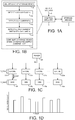
- FIG. 1A shows a data storage device according to an embodiment comprising a storage medium 2 and control circuitry 4 powered by a supply voltage 6 received from a voltage source.
- the control circuitry 4 is configured to execute the flow diagram of FIG. 1B wherein a load of the storage device is adjusted (block 8), a load voltage is detected at the adjusted load (block 10), and a load current is detected at the adjusted load (block 12).
- the detected load voltage and the detected load current are processed to detect a current limit of the voltage source (block 14), and the data storage device is configured in response to the detected current limit of the voltage source (block 16).
- FIG. 1C shows an embodiment wherein a number of data storage devices 18 1 -18 N are mounted into a chassis of a storage rack.
- a power supply 20 generates a supply voltage Vs and corresponding supply current applied to each data storage device through a current limiting electronic fuse (E-fuse) 22 1 -22 N .
- the DC current limit of each E-fuse may vary across the devices due to manufacturing tolerances.
- a transient response of the E-fuses may vary across the devices meaning that each E-fuse may conduct a different peak current during a transient load condition of the data storage device.
- each data storage device is configured so as to not exceed a minimum DC current limit of a worst case E-fuse, thereby ensuring none of the E-fuses open under all load conditions.
- configuring all of the data storage devices mounted in a chassis so as to not exceed the minimum DC current limit of the E-fuses means that at least some of the data storage devices will perform at a suboptimal level.
- the control circuitry 4 within each data storage device detects the current limit of its respective E-fuse, and then optimizes the operating performance, for example, to maximize a throughput of the data storage device based on the detected current limit.
- control circuitry 4 may detect a DC current limit and/or an AC current limit of its E-fuse in order to configure different operating modes of the data storage device (e.g., configure the maximum DC and AC loads corresponding to the respective current limits of the E-fuse).
- the control circuitry 4 may adjust a load of the data storage device while measuring a resistance of the E-fuse.
- the resistance of the E-fuse may be measured as the voltage across the E-fuse divided by the current flowing through the E-fuse.
- the voltage across the E-fuse (V_fuse) may be measured by subtracting a detected load voltage (V_load) within the data storage device from the known supply voltage Vs generated by the power supply 20 of FIG. 1C .
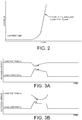
- the current limit of the E-fuse may then be detected when the measured resistance of the E-fuse exceeds a predetermined threshold as shown in FIG. 2 . That is, as a load within the data storage device increases, the supply current flowing through the E-fuse will increase until reaching the current limit of the E-fuse, thereby causing the resistance of the E-fuse to increase as the fuse transitions into an open state.
- FIGs. 3A and 3B show an alternative embodiment for detecting the current limit of the E-fuse.
- the control circuitry 4 monitors a slope polarity of a detected load voltage and a detected load current while adjusting a load of the data storage device. Referring to FIG. 3A , as the load current increases the load voltage decreases due to the load current increasing the voltage drop across the power supply 20 and E-fuse. If the current limit of the E-fuse is not reached, when the load current decreases (negative slope), there is a corresponding increase in the load voltage (positive slope) as shown in FIG. 3A .
- a transient load of the data storage device is increased until the slope polarity of the detected load voltage matches the slope polarity of the detected load current during at least part of the transient load condition.
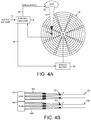
- FIG. 4A shows a data storage device in the form of a disk drive according to an embodiment comprising a spindle motor 24 configured to rotate a disk 26.
- a voice coil motor (VCM) 28 rotates an actuator arm 30 about a pivot in order to actuate a head 32 radially over the disk 26.
- the control circuitry 4 applies a control signal 34 to the spindle motor 24 in order to control a rotation speed of the disk 26, and applies a control signal 36 to the VCM 28 based on a seek profile in order to seek the head 32 over the disk 26 to access target data tracks.
- the disk drive may comprise multiple VCMs (e.g., VCM 28A and VCM 28B) configured to rotate respective sets of actuator arms 30A and 30B.
- the multiple VCMs may comprise a split-actuator configuration wherein the VCMs rotate their respective actuator arms about a common pivot as in the embodiment of FIG. 4B , or each VCM may actuate respective actuator arms about independent pivots.
- the control circuitry 4 when detecting the current limit of the E-fuse the control circuitry 4 increases a load of the disk drive by applying a driving current to either or both of the VCM(s) and/or to the spindle motor.
- the driving current may be applied to the VCM(s) and/or the spindle motor during normal access operations, or during a calibration procedure which may be executed periodically or when the disk drive is powered on.
- the control circuitry 4 may apply a driving current to the VCM 28 while the heads are parked on a ramp (e.g., drive the VCM 28 against a crash stop in order to increase a load of the disk drive).
- control circuitry 4 may apply a driving current concurrently to two or more VCMs in order to further increase the load of the disk drive (e.g., in an embodiment where each VCM may have a current limit before damaging the voice coil or run out of voltage headroom).
- when powered on the control circuitry 4 may apply a driving current to the spindle motor 24 while the spindle motor is stopped (e.g., by applying a driving current during a fixed commutation state of the spindle motor).
- the control circuitry 4 may confirm the spindle motor is not rotating (e.g., by evaluating the back electromotive force BEMF voltage of the spindle motor) before applying the driving current to the spindle motor during the calibration procedure.
- control circuitry 4 when powered on the control circuitry 4 may apply a driving current to the spindle motor in order to spin-up the disk(s) toward a target rotation speed and concurrently apply a driving current to at least one VCM (e.g., in order to drive the VCM toward a crash stop).
- This embodiment may reduce or eliminate any delay during power-on since the current limit of the E-fuse may be detected during the normal spin-up operation of the disk drive.
- the control circuitry 4 may configure the disk drive in any suitable manner based on the detected current limit of the E-fuse.
- the control circuitry 4 may configure a seek profile of the VCM 28, for example, by limiting a driving current during an acceleration and/or deceleration phase of a seek so as not to exceed the detected current limit of the E-fuse.
- the seek profiles for each VCM may be configured so that the combined current does not exceed the detected current limit of the E-fuse. An example of this embodiment is shown in FIG.
- a first seek profile 38 of a first VCM 28A and a second seek profile 40 of a second VCM 28B are configured so that the combined seek profile 42 does not exceed the detected current limit of the E-fuse.
- the disk drives powered through an E-fuse having a higher current limit may be configured to operate with higher performance by using more aggressive seek profiles.
- control circuitry may configure the seek profiles for multiple VCMs such that the combined current may exceed the DC current limit of the E-fuse for a short duration without exceeding the transient (AC) current limit of the E-fuse.
- the combined seek profile 42 in FIG. 5A may exceed the DC current limit for a transient duration
- the delay of the seek profiles in FIG. 5B may be configured so that the combined VCM current may exceed the DC current limit for a transient duration, thereby maximizing the performance without the E-fuse disrupting operation of the disk drive.
- a detected load voltage and a detected load current of the disk drive may be monitored while executing a seek operation of one or more VCMs in order to detect whether the current limit of the E-fuse is being exceeded.
- the control circuitry may modify the seek(s) in progress in order to prevent an overload condition.
- the control circuitry may adaptively adjust the detected current limit of the E-fuse based on whether the current limit is exceeded during normal seek operations. For example, in one embodiment the control circuitry may step increase the performance of the seek profiles (by increasing the seek current) until the current limit of the E-fuse is reached.
- the control circuitry may then back-off the performance of the seek profiles by a predetermined margin so as not to exceed the detect current limit during subsequent seek operations.
- the control circuitry may periodically step increase the performance of the seek profiles in order to recalibrate the detected current limit of the E-fuse.
- the current limit of the E-fuse may vary over time due, for example, to changes in environmental conditions (e.g., ambient temperature).
- the data storage device of FIG. 1A may comprise any suitable storage medium 2, wherein in an embodiment shown in FIG. 6 , the storage medium may comprise a non-volatile semiconductor memory (NVSM) 48 of a solid state drive (SSD).
- the non-volatile semiconductor memory 48 may comprise a number of individual memory devices, 50A, 50B, etc., for storing a number of data blocks.
- the control circuitry 4 may comprise multiple read channels as shown in FIG. 7A for concurrently accessing two or more of the memory devices in order to increase throughput. However, concurrently accessing multiple memory devices (or multiple disk surfaces) may exceed the current limit of the E-fuse.
- control circuitry 4 may configure an access throttling of the data storage device so as to not exceed the detected current limit of the E-fuse.
- An example of access throttling is shown in the embodiment of FIG. 7B wherein the operation of multiple read channels may be interleaved in order to reduce the combined load of the read channels.
- the amount of overlap between the multiple read channels may be adjusted based on the detected current limit (AC or DC) of the E-fuse.
- the access throttling may be implemented by adjusting a clock speed of multiple, overlapping read channels based on the detected current limit, wherein the clocking speed may be increased as the detected current limit increases.
- any suitable E-fuse 22 or E-fuse type device may be employed that is capable of limiting the maximum current flowing from the power supply 20 to the DSD 18.
- the E-fuse may comprise any suitable active circuitry, such as a field effect transistor (FET) controlled by current sensing circuitry.
- FET field effect transistor
- the E-fuse may operate as a transient fuse that may reset once the load current decreases below the current limit of the E-fuse.
- the E-fuse may comprise any suitable passive circuitry (e.g., a wire) that may exhibit an increased resistance prior to the E-fuse blowing.
- the control circuitry 4 within the DSD 18 may adjust the load current so as to prevent the E-fuse from reaching a blown (permanently disabled) state.
- control circuitry may be implemented within a read channel integrated circuit, or in a component separate from the read channel, such as a data storage controller, or certain operations described above may be performed by a read channel and others by a data storage controller.
- the read channel and data storage controller are implemented as separate integrated circuits, and in an alternative embodiment they are fabricated into a single integrated circuit or system on a chip (SOC).
- the control circuitry may include a suitable preamp circuit implemented as a separate integrated circuit, integrated into the read channel or data storage controller circuit, or integrated into a SOC.
- control circuitry comprises a microprocessor executing instructions, the instructions being operable to cause the microprocessor to perform the flow diagrams described herein.
- the instructions may be stored in any computer-readable medium. In one embodiment, they may be stored on a non-volatile semiconductor memory external to the microprocessor, or integrated with the microprocessor in a SOC. In another embodiment, the instructions are stored on the disk and read into a volatile semiconductor memory when the disk drive is powered on. In yet another embodiment, the control circuitry comprises suitable logic circuitry, such as state machine circuitry.
- At least some of the flow diagram blocks may be implemented using analog circuitry (e.g., analog comparators, timers, etc.), and in other embodiments at least some of the blocks may be implemented using digital circuitry or a combination of analog/digital circuitry.
- analog circuitry e.g., analog comparators, timers, etc.
- digital circuitry e.g., digital comparators, timers, etc.
Landscapes
- Engineering & Computer Science (AREA)
- Theoretical Computer Science (AREA)
- Physics & Mathematics (AREA)
- General Engineering & Computer Science (AREA)
- General Physics & Mathematics (AREA)
- Human Computer Interaction (AREA)
- Digital Magnetic Recording (AREA)
- Power Sources (AREA)
Applications Claiming Priority (1)
| Application Number | Priority Date | Filing Date | Title |
|---|---|---|---|
| US16/451,368 US11126248B2 (en) | 2019-06-25 | 2019-06-25 | Data storage device detecting supply current limit |
Publications (2)
| Publication Number | Publication Date |
|---|---|
| EP3757748A1 true EP3757748A1 (de) | 2020-12-30 |
| EP3757748B1 EP3757748B1 (de) | 2025-02-12 |
Family
ID=69779807
Family Applications (1)
| Application Number | Title | Priority Date | Filing Date |
|---|---|---|---|
| EP20161100.1A Active EP3757748B1 (de) | 2019-06-25 | 2020-03-05 | Datenspeichervorrichtung zur erfassung der versorgungsstromgrenze |
Country Status (3)
| Country | Link |
|---|---|
| US (1) | US11126248B2 (de) |
| EP (1) | EP3757748B1 (de) |
| CN (1) | CN112133331B (de) |
Families Citing this family (2)
| Publication number | Priority date | Publication date | Assignee | Title |
|---|---|---|---|---|
| US11126248B2 (en) * | 2019-06-25 | 2021-09-21 | Western Digital Technologies, Inc. | Data storage device detecting supply current limit |
| KR20210083941A (ko) * | 2019-12-27 | 2021-07-07 | 에스케이하이닉스 주식회사 | 메모리 시스템의 입출력 성능을 향상시키는 장치 및 방법 |
Citations (1)
| Publication number | Priority date | Publication date | Assignee | Title |
|---|---|---|---|---|
| US20040036471A1 (en) * | 2002-08-22 | 2004-02-26 | International Business Machines | Integrated field generator for actuating magnetic heads |
Family Cites Families (28)
| Publication number | Priority date | Publication date | Assignee | Title |
|---|---|---|---|---|
| US5844743A (en) | 1996-12-20 | 1998-12-01 | Seagate Technology, Inc. | Velocity sensing using actuator coil back-emf voltage |
| US6369972B1 (en) | 1999-05-14 | 2002-04-09 | Western Digital Technologies, Inc. | Temperature monitoring method of a disk drive voice coil motor from a traveled distance |
| AT410867B (de) | 2001-04-06 | 2003-08-25 | Siemens Ag Oesterreich | Spannungsversorgung mit abschaltsicherung |
| JP4180357B2 (ja) | 2002-11-25 | 2008-11-12 | 株式会社ルネサステクノロジ | 磁気ディスク記憶システム |
| US7362565B2 (en) | 2004-09-21 | 2008-04-22 | Dot Hill Systems Corporation | Disk drive support system |
| US7110214B1 (en) * | 2005-01-18 | 2006-09-19 | Western Digital Technologies, Inc. | Disk drive to implement a seek operation utilizing a deceleration velocity profile that mathematically models BEMFs |
| KR100688526B1 (ko) | 2005-01-28 | 2007-03-02 | 삼성전자주식회사 | 공급 전압 변동을 고려한 탐색 서보 제어 방법 및 이를이용한 디스크 드라이브 |
| US7765675B2 (en) | 2005-09-01 | 2010-08-03 | Hitachi Global Storage Technologies Netherlands B.V. | CPP read sensors having constrained current paths made of lithographically-defined conductive vias and methods of making the same |
| JP4203506B2 (ja) | 2006-01-13 | 2009-01-07 | シャープ株式会社 | 不揮発性半導体記憶装置及びその書き換え方法 |
| TWI408375B (zh) | 2009-06-05 | 2013-09-11 | Giga Byte Tech Co Ltd | 電流測量裝置以及電腦系統 |
| US8009502B2 (en) | 2009-06-24 | 2011-08-30 | Seagate Technology Llc | Systems, methods and devices for power control in mass storage devices |
| US8369092B2 (en) | 2010-04-27 | 2013-02-05 | International Business Machines Corporation | Input/output and disk expansion subsystem for an electronics rack |
| US9225158B2 (en) | 2011-09-14 | 2015-12-29 | Denso Corporation | Overcurrent protection circuit |
| US8630054B2 (en) | 2011-09-21 | 2014-01-14 | Western Digital Technologies, Inc. | Systems and methods for data throttling during disk drive power down |
| TWI430094B (zh) | 2011-09-22 | 2014-03-11 | Phison Electronics Corp | 記憶體儲存裝置、記憶體控制器與溫度管理方法 |
| US20130290611A1 (en) | 2012-03-23 | 2013-10-31 | Violin Memory Inc. | Power management in a flash memory |
| WO2014111920A1 (en) | 2013-01-17 | 2014-07-24 | Sure Erasure Ltd. | System and method for monitoring of an electro-mechanical device |
| US10383247B2 (en) | 2013-11-01 | 2019-08-13 | Quantra Computer Inc. | High density chassis for a server rack |
| US9093160B1 (en) | 2014-05-30 | 2015-07-28 | Sandisk Technologies Inc. | Methods and systems for staggered memory operations |
| US10014108B2 (en) | 2015-03-13 | 2018-07-03 | Avx Corporation | Low profile multi-anode assembly |
| US9424868B1 (en) | 2015-05-12 | 2016-08-23 | Western Digital Technologies, Inc. | Data storage device employing spindle motor driving profile during seek to improve power performance |
| US10394259B2 (en) | 2015-08-28 | 2019-08-27 | Stmicroelectronics S.R.L. | Current limiting electronic fuse circuit |
| JP2018156706A (ja) | 2017-03-17 | 2018-10-04 | 株式会社東芝 | 磁気ディスク装置 |
| EP3402072B1 (de) * | 2017-05-08 | 2021-06-30 | Hamilton Sundstrand Corporation | Einschaltstrombegrenzungssystem und verfahren |
| US10014018B1 (en) * | 2017-12-15 | 2018-07-03 | Western Digital Technologies, Inc. | Data storage device seeking multiple voice coil motors using a limited current supply |
| US10176840B1 (en) | 2018-06-28 | 2019-01-08 | Western Digital Technologies, Inc. | Data storage device adjusting spindle motor current based on continuous function of voice coil current during seek |
| US11126248B2 (en) * | 2019-06-25 | 2021-09-21 | Western Digital Technologies, Inc. | Data storage device detecting supply current limit |
| US10930310B1 (en) * | 2020-02-04 | 2021-02-23 | Western Digital Technologies, Inc. | Data storage device sorting access commands based on peak current for multiple actuators |
-
2019
- 2019-06-25 US US16/451,368 patent/US11126248B2/en active Active
-
2020
- 2020-03-05 EP EP20161100.1A patent/EP3757748B1/de active Active
- 2020-03-27 CN CN202010226890.3A patent/CN112133331B/zh active Active
Patent Citations (1)
| Publication number | Priority date | Publication date | Assignee | Title |
|---|---|---|---|---|
| US20040036471A1 (en) * | 2002-08-22 | 2004-02-26 | International Business Machines | Integrated field generator for actuating magnetic heads |
Also Published As
| Publication number | Publication date |
|---|---|
| US11126248B2 (en) | 2021-09-21 |
| EP3757748B1 (de) | 2025-02-12 |
| CN112133331B (zh) | 2021-11-23 |
| CN112133331A (zh) | 2020-12-25 |
| US20200409445A1 (en) | 2020-12-31 |
Similar Documents
| Publication | Publication Date | Title |
|---|---|---|
| US8630054B2 (en) | Systems and methods for data throttling during disk drive power down | |
| CN101017680B (zh) | 具有在意外断电时制动的自适应致动器的盘驱动器 | |
| JP4236797B2 (ja) | ディスクからヘッドをランプアンロードするための速度制御方法およびシステム | |
| CN109150032B (zh) | 电机驱动装置和电机系统 | |
| US10176840B1 (en) | Data storage device adjusting spindle motor current based on continuous function of voice coil current during seek | |
| US8405332B1 (en) | Method to eliminate current surge during spindle spin up | |
| US9940958B1 (en) | Data storage device employing delayed braking to unload multiple voice coil motors | |
| US10256751B2 (en) | Asymmetrical driver | |
| US20120112681A1 (en) | Current limiting for a motor winding | |
| JP2010146630A (ja) | ディスク・ドライブ及びディスク・アレイ・システム | |
| US10839839B1 (en) | Data storage device managing peak current for multiple actuators | |
| US10714133B1 (en) | Data storage device capable of overriding a servo command to avoid an overcurrent condition | |
| EP3757748B1 (de) | Datenspeichervorrichtung zur erfassung der versorgungsstromgrenze | |
| US9165583B1 (en) | Data storage device adjusting seek profile based on seek length when ending track is near ramp | |
| US20100148708A1 (en) | Voltage scaling of an electric motor load to reduce power consumption | |
| US8390226B1 (en) | Voltage mode using pseudo current limit | |
| US9997182B1 (en) | Data storage device employing balanced current drive to unload multiple voice coil motors | |
| US20100067140A1 (en) | Disk-Drive Read/Write Head Retraction Velocity Control | |
| US12148446B1 (en) | Power improvement for minimum switching frequency operation | |
| US12266385B2 (en) | Data storage device having dual actuators and method for emergency power off retract (EPOR) of dual actuators | |
| US7992029B2 (en) | Electronic device with temporary flag for fail safe and power cycling | |
| US7095201B1 (en) | Method and apparatus for providing a user selectable start-up current in a disk drive | |
| US11837264B2 (en) | Data storage device having dual actuators and method for data egress throttling during emergency power off retract (EPOR) | |
| US8218257B2 (en) | Disk drive with multiple level power reduction during write | |
| US9082451B2 (en) | Method of driving optical disc and optical disc drive using the method |
Legal Events
| Date | Code | Title | Description |
|---|---|---|---|
| PUAI | Public reference made under article 153(3) epc to a published international application that has entered the european phase |
Free format text: ORIGINAL CODE: 0009012 |
|
| STAA | Information on the status of an ep patent application or granted ep patent |
Free format text: STATUS: REQUEST FOR EXAMINATION WAS MADE |
|
| 17P | Request for examination filed |
Effective date: 20200309 |
|
| AK | Designated contracting states |
Kind code of ref document: A1 Designated state(s): AL AT BE BG CH CY CZ DE DK EE ES FI FR GB GR HR HU IE IS IT LI LT LU LV MC MK MT NL NO PL PT RO RS SE SI SK SM TR |
|
| AX | Request for extension of the european patent |
Extension state: BA ME |
|
| STAA | Information on the status of an ep patent application or granted ep patent |
Free format text: STATUS: EXAMINATION IS IN PROGRESS |
|
| 17Q | First examination report despatched |
Effective date: 20220701 |
|
| GRAP | Despatch of communication of intention to grant a patent |
Free format text: ORIGINAL CODE: EPIDOSNIGR1 |
|
| STAA | Information on the status of an ep patent application or granted ep patent |
Free format text: STATUS: GRANT OF PATENT IS INTENDED |
|
| RIC1 | Information provided on ipc code assigned before grant |
Ipc: G01R 31/74 20200101ALN20240826BHEP Ipc: H02H 3/087 20060101ALI20240826BHEP Ipc: G06F 3/06 20060101AFI20240826BHEP |
|
| INTG | Intention to grant announced |
Effective date: 20240909 |
|
| P01 | Opt-out of the competence of the unified patent court (upc) registered |
Free format text: CASE NUMBER: APP_51148/2024 Effective date: 20240910 |
|
| GRAS | Grant fee paid |
Free format text: ORIGINAL CODE: EPIDOSNIGR3 |
|
| GRAA | (expected) grant |
Free format text: ORIGINAL CODE: 0009210 |
|
| STAA | Information on the status of an ep patent application or granted ep patent |
Free format text: STATUS: THE PATENT HAS BEEN GRANTED |
|
| AK | Designated contracting states |
Kind code of ref document: B1 Designated state(s): AL AT BE BG CH CY CZ DE DK EE ES FI FR GB GR HR HU IE IS IT LI LT LU LV MC MK MT NL NO PL PT RO RS SE SI SK SM TR |
|
| REG | Reference to a national code |
Ref country code: GB Ref legal event code: FG4D |
|
| REG | Reference to a national code |
Ref country code: CH Ref legal event code: EP |
|
| REG | Reference to a national code |
Ref country code: DE Ref legal event code: R096 Ref document number: 602020045789 Country of ref document: DE |
|
| REG | Reference to a national code |
Ref country code: IE Ref legal event code: FG4D |
|
| REG | Reference to a national code |
Ref country code: NL Ref legal event code: FP |
|
| PG25 | Lapsed in a contracting state [announced via postgrant information from national office to epo] |
Ref country code: RS Free format text: LAPSE BECAUSE OF FAILURE TO SUBMIT A TRANSLATION OF THE DESCRIPTION OR TO PAY THE FEE WITHIN THE PRESCRIBED TIME-LIMIT Effective date: 20250512 |
|
| PG25 | Lapsed in a contracting state [announced via postgrant information from national office to epo] |
Ref country code: FI Free format text: LAPSE BECAUSE OF FAILURE TO SUBMIT A TRANSLATION OF THE DESCRIPTION OR TO PAY THE FEE WITHIN THE PRESCRIBED TIME-LIMIT Effective date: 20250212 |
|
| PG25 | Lapsed in a contracting state [announced via postgrant information from national office to epo] |
Ref country code: PL Free format text: LAPSE BECAUSE OF FAILURE TO SUBMIT A TRANSLATION OF THE DESCRIPTION OR TO PAY THE FEE WITHIN THE PRESCRIBED TIME-LIMIT Effective date: 20250212 |
|
| PG25 | Lapsed in a contracting state [announced via postgrant information from national office to epo] |
Ref country code: ES Free format text: LAPSE BECAUSE OF FAILURE TO SUBMIT A TRANSLATION OF THE DESCRIPTION OR TO PAY THE FEE WITHIN THE PRESCRIBED TIME-LIMIT Effective date: 20250212 |
|
| REG | Reference to a national code |
Ref country code: LT Ref legal event code: MG9D |
|
| PG25 | Lapsed in a contracting state [announced via postgrant information from national office to epo] |
Ref country code: IS Free format text: LAPSE BECAUSE OF FAILURE TO SUBMIT A TRANSLATION OF THE DESCRIPTION OR TO PAY THE FEE WITHIN THE PRESCRIBED TIME-LIMIT Effective date: 20250612 Ref country code: NO Free format text: LAPSE BECAUSE OF FAILURE TO SUBMIT A TRANSLATION OF THE DESCRIPTION OR TO PAY THE FEE WITHIN THE PRESCRIBED TIME-LIMIT Effective date: 20250512 |
|
| PG25 | Lapsed in a contracting state [announced via postgrant information from national office to epo] |
Ref country code: HR Free format text: LAPSE BECAUSE OF FAILURE TO SUBMIT A TRANSLATION OF THE DESCRIPTION OR TO PAY THE FEE WITHIN THE PRESCRIBED TIME-LIMIT Effective date: 20250212 |
|
| PG25 | Lapsed in a contracting state [announced via postgrant information from national office to epo] |
Ref country code: LV Free format text: LAPSE BECAUSE OF FAILURE TO SUBMIT A TRANSLATION OF THE DESCRIPTION OR TO PAY THE FEE WITHIN THE PRESCRIBED TIME-LIMIT Effective date: 20250212 Ref country code: PT Free format text: LAPSE BECAUSE OF FAILURE TO SUBMIT A TRANSLATION OF THE DESCRIPTION OR TO PAY THE FEE WITHIN THE PRESCRIBED TIME-LIMIT Effective date: 20250612 |
|
| PG25 | Lapsed in a contracting state [announced via postgrant information from national office to epo] |
Ref country code: BG Free format text: LAPSE BECAUSE OF FAILURE TO SUBMIT A TRANSLATION OF THE DESCRIPTION OR TO PAY THE FEE WITHIN THE PRESCRIBED TIME-LIMIT Effective date: 20250212 Ref country code: GR Free format text: LAPSE BECAUSE OF FAILURE TO SUBMIT A TRANSLATION OF THE DESCRIPTION OR TO PAY THE FEE WITHIN THE PRESCRIBED TIME-LIMIT Effective date: 20250513 |
|
| REG | Reference to a national code |
Ref country code: AT Ref legal event code: MK05 Ref document number: 1766678 Country of ref document: AT Kind code of ref document: T Effective date: 20250212 |
|
| PG25 | Lapsed in a contracting state [announced via postgrant information from national office to epo] |
Ref country code: SE Free format text: LAPSE BECAUSE OF FAILURE TO SUBMIT A TRANSLATION OF THE DESCRIPTION OR TO PAY THE FEE WITHIN THE PRESCRIBED TIME-LIMIT Effective date: 20250212 |
|
| PG25 | Lapsed in a contracting state [announced via postgrant information from national office to epo] |
Ref country code: SM Free format text: LAPSE BECAUSE OF FAILURE TO SUBMIT A TRANSLATION OF THE DESCRIPTION OR TO PAY THE FEE WITHIN THE PRESCRIBED TIME-LIMIT Effective date: 20250212 |
|
| PG25 | Lapsed in a contracting state [announced via postgrant information from national office to epo] |
Ref country code: DK Free format text: LAPSE BECAUSE OF FAILURE TO SUBMIT A TRANSLATION OF THE DESCRIPTION OR TO PAY THE FEE WITHIN THE PRESCRIBED TIME-LIMIT Effective date: 20250212 |
|
| PG25 | Lapsed in a contracting state [announced via postgrant information from national office to epo] |
Ref country code: IT Free format text: LAPSE BECAUSE OF FAILURE TO SUBMIT A TRANSLATION OF THE DESCRIPTION OR TO PAY THE FEE WITHIN THE PRESCRIBED TIME-LIMIT Effective date: 20250212 |
|
| PG25 | Lapsed in a contracting state [announced via postgrant information from national office to epo] |
Ref country code: AT Free format text: LAPSE BECAUSE OF FAILURE TO SUBMIT A TRANSLATION OF THE DESCRIPTION OR TO PAY THE FEE WITHIN THE PRESCRIBED TIME-LIMIT Effective date: 20250212 |
|
| PG25 | Lapsed in a contracting state [announced via postgrant information from national office to epo] |
Ref country code: EE Free format text: LAPSE BECAUSE OF FAILURE TO SUBMIT A TRANSLATION OF THE DESCRIPTION OR TO PAY THE FEE WITHIN THE PRESCRIBED TIME-LIMIT Effective date: 20250212 Ref country code: CZ Free format text: LAPSE BECAUSE OF FAILURE TO SUBMIT A TRANSLATION OF THE DESCRIPTION OR TO PAY THE FEE WITHIN THE PRESCRIBED TIME-LIMIT Effective date: 20250212 |
|
| PG25 | Lapsed in a contracting state [announced via postgrant information from national office to epo] |
Ref country code: RO Free format text: LAPSE BECAUSE OF FAILURE TO SUBMIT A TRANSLATION OF THE DESCRIPTION OR TO PAY THE FEE WITHIN THE PRESCRIBED TIME-LIMIT Effective date: 20250212 |
|
| REG | Reference to a national code |
Ref country code: CH Ref legal event code: H13 Free format text: ST27 STATUS EVENT CODE: U-0-0-H10-H13 (AS PROVIDED BY THE NATIONAL OFFICE) Effective date: 20251024 |
|
| PG25 | Lapsed in a contracting state [announced via postgrant information from national office to epo] |
Ref country code: SK Free format text: LAPSE BECAUSE OF FAILURE TO SUBMIT A TRANSLATION OF THE DESCRIPTION OR TO PAY THE FEE WITHIN THE PRESCRIBED TIME-LIMIT Effective date: 20250212 |
|
| REG | Reference to a national code |
Ref country code: NL Ref legal event code: MM Effective date: 20250401 |
|
| REG | Reference to a national code |
Ref country code: DE Ref legal event code: R097 Ref document number: 602020045789 Country of ref document: DE |
|
| PG25 | Lapsed in a contracting state [announced via postgrant information from national office to epo] |
Ref country code: LU Free format text: LAPSE BECAUSE OF NON-PAYMENT OF DUE FEES Effective date: 20250305 |
|
| REG | Reference to a national code |
Ref country code: BE Ref legal event code: MM Effective date: 20250331 |
|
| PG25 | Lapsed in a contracting state [announced via postgrant information from national office to epo] |
Ref country code: NL Free format text: LAPSE BECAUSE OF NON-PAYMENT OF DUE FEES Effective date: 20250401 |
|
| PLBE | No opposition filed within time limit |
Free format text: ORIGINAL CODE: 0009261 |
|
| STAA | Information on the status of an ep patent application or granted ep patent |
Free format text: STATUS: NO OPPOSITION FILED WITHIN TIME LIMIT |
|
| PG25 | Lapsed in a contracting state [announced via postgrant information from national office to epo] |
Ref country code: MC Free format text: LAPSE BECAUSE OF FAILURE TO SUBMIT A TRANSLATION OF THE DESCRIPTION OR TO PAY THE FEE WITHIN THE PRESCRIBED TIME-LIMIT Effective date: 20250212 |
|
| PG25 | Lapsed in a contracting state [announced via postgrant information from national office to epo] |
Ref country code: FR Free format text: LAPSE BECAUSE OF NON-PAYMENT OF DUE FEES Effective date: 20250412 |
|
| PG25 | Lapsed in a contracting state [announced via postgrant information from national office to epo] |
Ref country code: BE Free format text: LAPSE BECAUSE OF NON-PAYMENT OF DUE FEES Effective date: 20250331 |
|
| PG25 | Lapsed in a contracting state [announced via postgrant information from national office to epo] |
Ref country code: CH Free format text: LAPSE BECAUSE OF NON-PAYMENT OF DUE FEES Effective date: 20250331 |
|
| PG25 | Lapsed in a contracting state [announced via postgrant information from national office to epo] |
Ref country code: IE Free format text: LAPSE BECAUSE OF NON-PAYMENT OF DUE FEES Effective date: 20250305 |
|
| 26N | No opposition filed |
Effective date: 20251113 |
|
| PGFP | Annual fee paid to national office [announced via postgrant information from national office to epo] |
Ref country code: GB Payment date: 20260119 Year of fee payment: 7 |
|
| PGFP | Annual fee paid to national office [announced via postgrant information from national office to epo] |
Ref country code: DE Payment date: 20260114 Year of fee payment: 7 |