EP3757734A1 - Touch sensitive display device with reduced bezel area - Google Patents
Touch sensitive display device with reduced bezel area Download PDFInfo
- Publication number
- EP3757734A1 EP3757734A1 EP20182272.3A EP20182272A EP3757734A1 EP 3757734 A1 EP3757734 A1 EP 3757734A1 EP 20182272 A EP20182272 A EP 20182272A EP 3757734 A1 EP3757734 A1 EP 3757734A1
- Authority
- EP
- European Patent Office
- Prior art keywords
- touch
- disposed
- display
- lines
- area
- Prior art date
- Legal status (The legal status is an assumption and is not a legal conclusion. Google has not performed a legal analysis and makes no representation as to the accuracy of the status listed.)
- Granted
Links
Images




Classifications
-
- G—PHYSICS
- G06—COMPUTING OR CALCULATING; COUNTING
- G06F—ELECTRIC DIGITAL DATA PROCESSING
- G06F3/00—Input arrangements for transferring data to be processed into a form capable of being handled by the computer; Output arrangements for transferring data from processing unit to output unit, e.g. interface arrangements
- G06F3/01—Input arrangements or combined input and output arrangements for interaction between user and computer
- G06F3/03—Arrangements for converting the position or the displacement of a member into a coded form
- G06F3/041—Digitisers, e.g. for touch screens or touch pads, characterised by the transducing means
- G06F3/0416—Control or interface arrangements specially adapted for digitisers
- G06F3/04164—Connections between sensors and controllers, e.g. routing lines between electrodes and connection pads
-
- G—PHYSICS
- G06—COMPUTING OR CALCULATING; COUNTING
- G06F—ELECTRIC DIGITAL DATA PROCESSING
- G06F3/00—Input arrangements for transferring data to be processed into a form capable of being handled by the computer; Output arrangements for transferring data from processing unit to output unit, e.g. interface arrangements
- G06F3/01—Input arrangements or combined input and output arrangements for interaction between user and computer
- G06F3/03—Arrangements for converting the position or the displacement of a member into a coded form
- G06F3/041—Digitisers, e.g. for touch screens or touch pads, characterised by the transducing means
-
- G—PHYSICS
- G06—COMPUTING OR CALCULATING; COUNTING
- G06F—ELECTRIC DIGITAL DATA PROCESSING
- G06F3/00—Input arrangements for transferring data to be processed into a form capable of being handled by the computer; Output arrangements for transferring data from processing unit to output unit, e.g. interface arrangements
- G06F3/01—Input arrangements or combined input and output arrangements for interaction between user and computer
- G06F3/03—Arrangements for converting the position or the displacement of a member into a coded form
- G06F3/041—Digitisers, e.g. for touch screens or touch pads, characterised by the transducing means
- G06F3/0412—Digitisers structurally integrated in a display
-
- G—PHYSICS
- G06—COMPUTING OR CALCULATING; COUNTING
- G06F—ELECTRIC DIGITAL DATA PROCESSING
- G06F3/00—Input arrangements for transferring data to be processed into a form capable of being handled by the computer; Output arrangements for transferring data from processing unit to output unit, e.g. interface arrangements
- G06F3/01—Input arrangements or combined input and output arrangements for interaction between user and computer
- G06F3/03—Arrangements for converting the position or the displacement of a member into a coded form
- G06F3/041—Digitisers, e.g. for touch screens or touch pads, characterised by the transducing means
- G06F3/044—Digitisers, e.g. for touch screens or touch pads, characterised by the transducing means by capacitive means
- G06F3/0443—Digitisers, e.g. for touch screens or touch pads, characterised by the transducing means by capacitive means using a single layer of sensing electrodes
-
- G—PHYSICS
- G06—COMPUTING OR CALCULATING; COUNTING
- G06F—ELECTRIC DIGITAL DATA PROCESSING
- G06F3/00—Input arrangements for transferring data to be processed into a form capable of being handled by the computer; Output arrangements for transferring data from processing unit to output unit, e.g. interface arrangements
- G06F3/01—Input arrangements or combined input and output arrangements for interaction between user and computer
- G06F3/03—Arrangements for converting the position or the displacement of a member into a coded form
- G06F3/041—Digitisers, e.g. for touch screens or touch pads, characterised by the transducing means
- G06F3/044—Digitisers, e.g. for touch screens or touch pads, characterised by the transducing means by capacitive means
- G06F3/0446—Digitisers, e.g. for touch screens or touch pads, characterised by the transducing means by capacitive means using a grid-like structure of electrodes in at least two directions, e.g. using row and column electrodes
-
- H—ELECTRICITY
- H10—SEMICONDUCTOR DEVICES; ELECTRIC SOLID-STATE DEVICES NOT OTHERWISE PROVIDED FOR
- H10K—ORGANIC ELECTRIC SOLID-STATE DEVICES
- H10K50/00—Organic light-emitting devices
- H10K50/80—Constructional details
- H10K50/805—Electrodes
- H10K50/81—Anodes
-
- H—ELECTRICITY
- H10—SEMICONDUCTOR DEVICES; ELECTRIC SOLID-STATE DEVICES NOT OTHERWISE PROVIDED FOR
- H10K—ORGANIC ELECTRIC SOLID-STATE DEVICES
- H10K50/00—Organic light-emitting devices
- H10K50/80—Constructional details
- H10K50/84—Passivation; Containers; Encapsulations
- H10K50/844—Encapsulations
-
- H—ELECTRICITY
- H10—SEMICONDUCTOR DEVICES; ELECTRIC SOLID-STATE DEVICES NOT OTHERWISE PROVIDED FOR
- H10K—ORGANIC ELECTRIC SOLID-STATE DEVICES
- H10K59/00—Integrated devices, or assemblies of multiple devices, comprising at least one organic light-emitting element covered by group H10K50/00
- H10K59/10—OLED displays
- H10K59/12—Active-matrix OLED [AMOLED] displays
- H10K59/131—Interconnections, e.g. wiring lines or terminals
-
- H—ELECTRICITY
- H10—SEMICONDUCTOR DEVICES; ELECTRIC SOLID-STATE DEVICES NOT OTHERWISE PROVIDED FOR
- H10K—ORGANIC ELECTRIC SOLID-STATE DEVICES
- H10K59/00—Integrated devices, or assemblies of multiple devices, comprising at least one organic light-emitting element covered by group H10K50/00
- H10K59/30—Devices specially adapted for multicolour light emission
- H10K59/38—Devices specially adapted for multicolour light emission comprising colour filters or colour changing media [CCM]
-
- H—ELECTRICITY
- H10—SEMICONDUCTOR DEVICES; ELECTRIC SOLID-STATE DEVICES NOT OTHERWISE PROVIDED FOR
- H10K—ORGANIC ELECTRIC SOLID-STATE DEVICES
- H10K59/00—Integrated devices, or assemblies of multiple devices, comprising at least one organic light-emitting element covered by group H10K50/00
- H10K59/40—OLEDs integrated with touch screens
-
- H—ELECTRICITY
- H10—SEMICONDUCTOR DEVICES; ELECTRIC SOLID-STATE DEVICES NOT OTHERWISE PROVIDED FOR
- H10K—ORGANIC ELECTRIC SOLID-STATE DEVICES
- H10K59/00—Integrated devices, or assemblies of multiple devices, comprising at least one organic light-emitting element covered by group H10K50/00
- H10K59/80—Constructional details
- H10K59/87—Passivation; Containers; Encapsulations
- H10K59/873—Encapsulations
- H10K59/8731—Encapsulations multilayered coatings having a repetitive structure, e.g. having multiple organic-inorganic bilayers
-
- H—ELECTRICITY
- H10—SEMICONDUCTOR DEVICES; ELECTRIC SOLID-STATE DEVICES NOT OTHERWISE PROVIDED FOR
- H10K—ORGANIC ELECTRIC SOLID-STATE DEVICES
- H10K77/00—Constructional details of devices covered by this subclass and not covered by groups H10K10/80, H10K30/80, H10K50/80 or H10K59/80
- H10K77/10—Substrates, e.g. flexible substrates
- H10K77/111—Flexible substrates
-
- G—PHYSICS
- G06—COMPUTING OR CALCULATING; COUNTING
- G06F—ELECTRIC DIGITAL DATA PROCESSING
- G06F2203/00—Indexing scheme relating to G06F3/00 - G06F3/048
- G06F2203/041—Indexing scheme relating to G06F3/041 - G06F3/045
- G06F2203/04102—Flexible digitiser, i.e. constructional details for allowing the whole digitising part of a device to be flexed or rolled like a sheet of paper
-
- G—PHYSICS
- G06—COMPUTING OR CALCULATING; COUNTING
- G06F—ELECTRIC DIGITAL DATA PROCESSING
- G06F2203/00—Indexing scheme relating to G06F3/00 - G06F3/048
- G06F2203/041—Indexing scheme relating to G06F3/041 - G06F3/045
- G06F2203/04103—Manufacturing, i.e. details related to manufacturing processes specially suited for touch sensitive devices
Definitions
- a minimum of M touch lines (M being a natural number greater than 1 and less than N) is disposed with respect to a minimum of N display link lines (N being a natural number greater than 1), among the plurality of display link lines, in the non-active area, whereby a narrow bezel may be realized
- the adhesive reinforcement layer may be made of a material comprising indium.
- the plurality of touch electrodes 150 may be formed so as to have the same or similar size. Consequently, a deviation in touch sensitivity of the plurality of touch electrodes 150 is minimized or reduced, whereby it is possible to reduce noise.
- the touch electrodes 150 are connected to touch lines 152 in the active area AA.
- the first link area LA1 is disposed between the active area AA and the bending area BA.
- the switching transistor T1 When a scan pulse is supplied to a scan line SL, the switching transistor T1 is turned on to supply a data signal Vdata, which has been supplied to a data line DL, to the storage capacitor Cst and to a gate electrode of the drive transistor T2.
- the drive transistor T2 controls current that is supplied from a high-voltage (VDD) supply line to the light-emitting element 120 to adjust the amount of light emitted by the light-emitting element 120. Even when the switching transistor T1 is turned off, the drive transistor T2 supplies uniform current to the light-emitting element 120 using voltage charged in the storage capacitor Cst such that the light-emitting element 120 keeps emitting light until a data signal of the next frame is supplied.
- VDD high-voltage
- At least one dam 110 is disposed to prevent the organic encapsulation layer 144 from spreading to the non-active area NA.
- the at least one dam 110 is made of the same material as at least one of the pixel planarization layer 166, the bank 128, or a spacer (not shown).
- a first dam 1101 which is the most adjacent to the active area AA, is formed by sequentially stacking a second sub dam 110b made of the same material as the bank 128 and a third sub dam 110c made of the same material as the spacer.
- the display pad 180 and the touch pad 170 disposed in the pad area PA are disposed at different rows, as shown in FIGs. 1 and 3 .
- the touch pads 170 are disposed at a first row, which is the closest to (the farthest from) the active area AA
- the display pads 180 are disposed at second to fourth rows, which are far from (close to) the active area AA.
- the touch pad 170 and the display pad 180 are disposed at a plurality of rows, it is possible to reduce the length of the area occupied by the touch pad 170 and the display pad 180 in the pad area PA, compared to a comparative example in which the touch pad 170 and the display pad 180 are disposed in a line. That is, the length of the area occupied by the touch pad 170 and the display pad 180 disposed at the plurality of rows in the pad area PA is less than the length of the signal transmission film 202 on which the integrated touch display drive IC (TDDI) connected to the touch pad 170 and the display pad 180 is mounted.
- TDDI integrated touch display drive IC
- the second touch pad electrode 174 is made of the same material as the second touch line 152b, and is disposed on the upper interlayer dielectric film 118.
- the second touch pad electrode 174 is electrically connected to the first touch pad electrode 172 exposed through a touch pad contact hole 178 formed through the upper interlayer dielectric film 118.
- a third display link line 154c is also disposed on a different layer from another third display link line 154c and a third touch line 152c adjacent thereto.
- an odd (even)-number-th third display link line 154c is made of the same material as the gate electrode 132, and is disposed on the gate dielectric film 114, which is the same plane as the gate electrode 132.
- an even (odd)-number-th third display link line 154c or third touch line 152c is made of the same material as the fourth storage electrode 108, and is disposed on the lower interlayer dielectric film 116, which is the same plane as the fourth storage electrode 108.
- the outer signal lines including the display link lines 154 and the touch lines 152 are alternately disposed on different layers, as shown in FIG. 7 . That is, an outer signal line disposed at the upper side (the lower side) is disposed between outer signal lines disposed at the lower side (the upper side). At this time, the difference between the line width of the outer signal line disposed at the upper side (the lower side) and the distance between the outer signal lines disposed at the lower side (the upper side) is a maximum of 0.2 ⁇ m.
- the touch passivation film 168 which is made of an organic film, has low interface adhesive strength with each of the touch line 152, the third touch pad electrode 176, and the third display pad electrode 186.
- no subsequent manufacturing process is performed after the touch passivation film 168 is formed, and therefore it is possible to reduce separation of the touch passivation film 168 from each the touch line 152, the third touch pad electrode 176, and the third display pad electrode 186.
- a signal is properly supplied through the touch line 152, the third touch pad electrode 176, and the third display pad electrode 186.
- the signal pads including the display pads and the touch pads disposed in the pad area are disposed at a plurality of rows in the pad area, whereby it is possible to prevent electrical short circuit between the signal pads.
Landscapes
- Engineering & Computer Science (AREA)
- Theoretical Computer Science (AREA)
- General Engineering & Computer Science (AREA)
- Physics & Mathematics (AREA)
- Human Computer Interaction (AREA)
- General Physics & Mathematics (AREA)
- Optics & Photonics (AREA)
- Microelectronics & Electronic Packaging (AREA)
- Chemical & Material Sciences (AREA)
- Inorganic Chemistry (AREA)
- Computer Networks & Wireless Communication (AREA)
- Devices For Indicating Variable Information By Combining Individual Elements (AREA)
- Electroluminescent Light Sources (AREA)
Abstract
Description
- This application claims the priority of Republic of Korea Patent Application No.
10-2019-0077792, filed on June 28, 2019 - The present disclosure relates to a display device, and more particularly to a display device having a reduced bezel area.
- A touchscreen is an input device that allows a user to input a command by selecting one of instructions displayed on a screen, such as that of a display device, using a user's hand or an object. That is, the touchscreen converts the contact position, at which the user's hand or the object directly contacts the touchscreen, into an electrical signal to receive the instruction selected at the contact position as an input signal. Use of the touchscreen has increased, since the touchscreen is capable of replacing a separate input device that is connected to the display device for operation, such as a keyboard or a mouse.
- In recent years, research has been actively conducted on an integrated display device in which the touchscreen is disposed on a display panel, such as a liquid crystal display panel or an organic electroluminescent display panel. Touch lines configured to drive the touchscreen and display lines configured to drive the display panel are disposed in a bezel area, which is a non-display area, of the integrated display device, whereby it is difficult to reduce the width of the bezel area. In particular, a self-capacitance touchscreen has a larger number of touch lines than a capacitive touchscreen, whereby an integrated display device including a self-capacitance touchscreen has a problem in that the space of the bezel area in which display link lines connected to the display lines and the touch lines are disposed is insufficient.
- Furthermore, a signal transmission film attached to the bezel area has a smaller length than the bezel area. In this case, the distance between signal pads electrically connected to the signal transmission film is less than the distance between the display link lines and the touch lines, whereby electrical short circuit occurs between the signal pads.
- Accordingly, the present disclosure is directed to a display device that substantially obviates one or more problems due to limitations and disadvantages of the related art.
- An object of the present invention is to provide a display device having a reduced bezel area without electrical short circuit between signal pads.
- Additional advantages, objects, and features of the invention will be set forth in part in the description which follows and in part will become apparent to those having ordinary skill in the art upon examination of the following or may be learned from practice of the disclosure. The objectives and other advantages of the disclosure may be realized and attained by the structure particularly pointed out in the written description and claims hereof as well as the appended drawings.
- The object is solved by the features of the independent claims. Preferred embodiments are given in the dependent claims.
- To achieve these objects and other advantages and in accordance with the purpose of the disclosure, as embodied and broadly described herein, a display device includes a plurality of touch lines electrically connected to a plurality of touch electrodes disposed on an encapsulation unit and display link lines electrically connected to a light-emitting element, the display link lines being disposed in a non-active area of a substrate.
- A minimum of M touch lines (M being a natural number greater than 1 and less than N) is disposed with respect to a minimum of N display link lines (N being a natural number greater than 1), among the plurality of display link lines, in the non-active area, whereby a narrow bezel may be realized
- In some embodiments, the display device may further comprise touch pads connected to the plurality of touch lines; and/or display pads connected to the plurality of display link lines.
- In some embodiments, the non-active area may comprise at least one of a pad area in which the touch pads and the display pads are disposed; and/or a first link area adjacent to the active area; and/or a second link area disposed between the first link area and the pad area; and/or a bending area disposed between the first link area and the second link area.
- In some embodiments, each of outer signal lines may comprise the display link lines.
- Preferably, the touch lines may be alternately disposed on a different layer from an outer signal line adjacent thereto in the second link area.
- In some embodiments, the touch lines may be made of different materials and/or may be disposed on different layers in the first link area, the bending area, and the second link area.
- In some embodiments, the display device may further comprise a transistor connected to the light-emitting element.
- Preferably, the touch lines may comprise first touch lines disposed in the first link area, and/or second touch lines disposed in the bending area, and/or third touch lines disposed in the second link area.
- Preferably, the second touch lines may be formed of a same material as source and drain electrodes of the transistor.
- Preferably, the first touch lines may be formed of a same material as the touch electrodes.
- Preferably, the third touch lines may be disposed at a lower layer than the second touch lines.
- In some embodiments, the touch pads and the display pads may be disposed at different rows.
- Preferably, the display link lines may be disposed between the touch pads, or the touch lines may be disposed between the display pads.
- In some embodiments, the display device may further comprise a crack prevention layer disposed in the bending area.
- Preferably, the crack prevention layer may be on the touch lines and the display link lines.
- Preferably, an adhesive reinforcement layer may disposed between each of the touch lines and the display link lines and the crack prevention layer.
- Preferably, the adhesive reinforcement layer may be made of a material comprising indium.
- Preferably, the adhesive reinforcement layer may be formed of a same material as an anode of the light-emitting element.
- In some embodiments, the display device may further comprise a color filter disposed above or under each of the touch electrodes.
- In another aspect of the disclosure a display device is provided, comprising: a light-emitting element disposed in an active area of a substrate; an encapsulation unit disposed on the light-emitting element; a plurality of touch electrodes disposed on the encapsulation unit; display link lines electrically connected to the light-emitting element, the display link lines being disposed in a non-active area of the substrate; and a plurality of touch lines electrically connected to the plurality of touch electrodes, wherein at least one touch line is disposed between the display link lines disposed in a bending area, which is a portion of the non-active area.
- In some embodiments, the display device may further comprise touch pads connected to the plurality of touch lines; and/or display pads connected to the plurality of display link lines.
- In some embodiments, the non-active area may comprise the bending area; a pad area in which the touch pads and the display pads are disposed; a first link area disposed between the active area and the bending area; and a second link area disposed between the first link area and the pad area.
- In some embodiments, each of outer signal lines comprising the display link lines and the touch lines may be alternately disposed on a different layer from an outer signal line adjacent thereto in the second link area.
- In some embodiments, the touch pads and the display pads may be disposed at different rows, and/or the display link lines may be disposed between the touch pads, or the touch lines may be disposed between the display pads.
- In some embodiments, the display device may further comprise a crack prevention layer disposed in the bending area.
- Preferably, the crack prevention layer may be disposed on the touch lines and the display link lines.
- Preferably, an adhesive reinforcement layer may be disposed between each of the touch lines and the display link lines and the crack prevention layer.
- Preferably, the adhesive reinforcement layer may be formed of a material comprising indium
- Preferably, the display device may further comprise a color filter disposed above or under each of the touch electrodes.
- It is to be understood that both the foregoing general description and the following detailed description of the present disclosure are exemplary and explanatory and are intended to provide further explanation of the disclosure as claimed.
- The accompanying drawings, which are included to provide a further understanding of the disclosure and are incorporated in and constitute a part of this application, illustrate embodiment(s) of the disclosure and together with the description serve to explain the principle of the disclosure. In the drawings:
-
FIG. 1 is a plan view showing a display device according to a first embodiment of the present disclosure. -
FIG. 2 is a sectional view showing the state in which the display device shown inFIG. 1 is bent according to an embodiment of the present disclosure. -
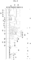
FIG. 3 is an enlarged plan view of area A ofFIG. 1 of an embodiment of the present disclosure. -
FIG. 4 is a sectional view of the display device taken along line I-I' ofFIG. 3 according to an embodiment of the present disclosure. -
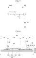
FIG. 5 is a circuit diagram showing each subpixel shown inFIG. 3 , of an embodiment of the present disclosure. -
FIG. 6 is a sectional view of the display device taken along line II-II' ofFIG. 3 , according to an embodiment of the present disclosure. -
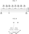
FIG. 7 is a sectional view of the display device taken along lines III1-III1' and III2-II12' ofFIG. 3 , according to an embodiment of the present disclosure. -
FIG. 8 is a sectional view of the display device taken along line IV-IV' ofFIG. 3 , according to an embodiment of the present disclosure. -
FIG. 9 is a sectional view showing a display device of a second embodiment of the disclosure. -
FIG. 10 is a sectional view showing a display device of a third embodiment of the disclosure. - Hereinafter, embodiments of the present disclosure will be described in detail with reference to the accompanying drawings.
-
FIG. 1 is a plan view showing a display device according to a first embodiment of the present disclosure. - The display device shown in
FIG. 1 is divided into an active area AA and a non-active area NA provided on asubstrate 101. - A plurality of display elements and a plurality of
touch electrodes 150 are disposed in the active area AA. Each of the plurality oftouch electrodes 150 includes capacitance formed therein and thus is used as a self-capacitance touch sensor configured to sense a change in capacitance due to user touch. In a self-capacitance sensing method using such atouch electrode 150, electric charge is accumulated in a touch sensor when a drive signal supplied through atouch line 152 is applied to thetouch electrode 150. At this time, when a user's finger or a conductive object contacts thetouch electrode 150, parasitic capacitance is additionally connected to a self-capacitance sensor, whereby the value of capacitance is changed. Consequently, the value of capacitance of the touch sensor touched by the finger is different from the value of capacitance of a touch sensor not touched by the finger, whereby it is possible to determine whether touch has been performed. - The plurality of
touch electrodes 150 may be formed so as to have the same or similar size. Consequently, a deviation in touch sensitivity of the plurality oftouch electrodes 150 is minimized or reduced, whereby it is possible to reduce noise. Thetouch electrodes 150 are connected to touchlines 152 in the active area AA. - The non-active area NA is disposed in the vicinity of the active area AA. For example, the non-active area NA is disposed at at least one of the upper side, lower side, the left side, or the right side of the active area AA.
- The non-active area NA includes at least one of a first and second link areas LA1 and LA2, a bending area BA, and a pad area PA.
- The first link area LA1 is disposed between the active area AA and the bending area BA.
- The second link area LA2 is disposed between the bending area BA and the pad area PA. Lighting inspection transistors are disposed in the second link area LA2.
- The bending area BA is an area in which the
substrate 101 is bendable or foldable, as shown inFIG. 2 , and corresponds to an area that is bent in order to locate the non-active area NA at the rear of the active area AA. In the entire screen of the display device, the area occupied by the active area AA is maximized or increased and the area corresponding to the non-active area NA is minimized or decreased by the bending area BA. The bending area BA may be disposed in at least one of the upper side, the lower side, the left side, or the right side of the non-active area NA. -
Display link lines 154 connected to the display elements andtouch lines 152 connected to thetouch electrodes 150 are disposed in the first and second link areas LA1 and LA2 and the bending area BA. In the bending area BA, each of thetouch lines 152 and thedisplay link lines 154 is disposed in a zigzag fashion, or a plurality of hollow polygonal structures, a plurality of hollow circular structures, or combinations thereof are connected to each other and disposed in a line. Consequently, it is possible to reduce damage to thetouch lines 152 and/or thedisplay link lines 154 even when bending force is applied to the bending area BA. -
Display pads 180 connected to the plurality ofdisplay link lines 154 andtouch pads 170 connected to the plurality oftouch lines 152 are disposed in the pad area PA. As shown inFig. 2 , thedisplay pads 180 and thetouch pads 170 are electrically connected to asignal transmission film 202 on which a drive integratedcircuit 204 is mounted. Here, the drive integratedcircuit 204 may be realized by an integrated touch display drive IC (TDDI) in which a display drive circuit configured to drive the display elements and a touch drive circuit configured to drive thetouch electrodes 150 are integrated. - The display elements disposed in the active area AA may be a liquid crystal element or a light-emitting element.. Particularly, in the present disclosure, a display device in which a light-emitting element shown in
FIGs. 3 and4 is applied as a display element will be described by way of example. - An organic light-emitting display device having a touch sensor shown in
FIGs. 3 and4 includes asubstrate 101, a plurality of subpixels disposed on thesubstrate 101 in a matrix form, anencapsulation unit 140 disposed on the plurality of subpixels, and atouch electrode 150 disposed on theencapsulation unit 140. - The
substrate 101 is made of a plastic material or a glass material having flexibility so as to be foldable or bendable. For example, thesubstrate 101 may be made of polyimide (PI), polyethylene terephthalate (PET), polyethylene naphthalate (PEN), polycarbonate (PC), polyethersulfone (PES), polyacrylate (PAR), polysulfone (PSF), or cyclic-olefin copolymer (COC). - The plurality of subpixels includes red (R), green (G), and blue (B) subpixels or red (R), green (G), blue (B), and white (W) subpixels. Each of the plurality of subpixels includes a pixel drive circuit and a light-emitting
element 120 connected to the pixel drive circuit. - As shown in
FIG. 5 , the pixel drive circuit includes a switching transistor T1, a drive transistor T2, and a storage capacitor Cst. In the present disclosure, the pixel drive circuit has been described as including two transistors T and one capacitor C by way of example. However, the present disclosure is not limited thereto. That is, a 3T1C or 3T2C type pixel drive circuit having three or more transistors T and one or more capacitors C may be used. - When a scan pulse is supplied to a scan line SL, the switching transistor T1 is turned on to supply a data signal Vdata, which has been supplied to a data line DL, to the storage capacitor Cst and to a gate electrode of the drive transistor T2.
- In response to the data signal supplied to the gate electrode of the drive transistor T2, the drive transistor T2 controls current that is supplied from a high-voltage (VDD) supply line to the light-emitting
element 120 to adjust the amount of light emitted by the light-emittingelement 120. Even when the switching transistor T1 is turned off, the drive transistor T2 supplies uniform current to the light-emittingelement 120 using voltage charged in the storage capacitor Cst such that the light-emittingelement 120 keeps emitting light until a data signal of the next frame is supplied. - To this end, as shown in
FIG. 4 , thedrive transistor 130 includes asemiconductor layer 134 disposed on abuffer layer 112, agate electrode 132 overlapping thesemiconductor layer 134 in the state in which agate dielectric film 114 is disposed therebetween, and source and drainelectrodes interlayer dielectric film 118 so as to contact thesemiconductor layer 134. - The
semiconductor layer 134 is made of at least one of an amorphous semiconductor material, a polycrystalline semiconductor material, or an oxide semiconductor material. Thesemiconductor layer 134 includes a channel area, a source area, and a drain area. The channel area overlaps thegate electrode 132 in the state in which thegate dielectric film 114 is disposed therebetween so as to be formed between the source and drainelectrodes source electrode 136 via a source contact hole, which is formed through thegate dielectric film 114 and interlayerdielectric films drain electrode 138 via a drain contact hole, which is formed through thegate dielectric film 114 and the interlayerdielectric films - The
buffer layer 112, which is disposed between thesemiconductor layer 134 and thesubstrate 101, blocks moisture and/or oxygen that has permeated into thesubstrate 101 to protect thesemiconductor layer 134. Thebuffer layer 112 is made of at least one of SiNx or SiOx, and has an at least single-layered structure. - The
gate electrode 132 may be made of one of molybdenum (Mo), aluminum (Al), chromium (Cr), gold (Au), titanium (Ti), nickel (Ni), neodymium (Nd), and copper (Cu) or an alloy thereof, and may have a single-layered structure or a multi-layered structure. However, the present disclosure is not limited thereto. Thegate electrode 132 overlaps the channel area of thesemiconductor layer 134 in the state in which thegate dielectric film 114 is disposed therebetween. - Each of the source and drain
electrodes source electrode 136 is connected to the source area of thesemiconductor layer 134 exposed through the source contact hole, which is formed through thegate dielectric film 114 and the lower and upper interlayerdielectric films drain electrode 138 faces thesource electrode 136, and is connected to the drain area of thesemiconductor layer 134 via the drain contact hole, which is formed through thegate dielectric film 114 and the lower and upper interlayerdielectric films - As shown in
FIG. 4 , the storage capacitor Cst includes at least two of first tofourth storage electrodes first storage electrode 102 is formed on thebuffer layer 112, and is made of the same material as thesemiconductor layer 134. Thesecond storage electrode 104 is formed on thegate dielectric film 114, and is made of the same material as thegate electrode 132. Thethird storage electrode 106 is formed on the lowerinterlayer dielectric film 116, and is made of the same material as athird touch line 152c. Thefourth storage electrode 108 is formed on the upperinterlayer dielectric film 118, and is made of the same material as the source and drainelectrodes - The light-emitting
element 120 includes ananode 122, at least one light-emittingstack 124 formed on theanode 122, and acathode 126 formed on the light-emittingstack 124. - The
anode 122 is electrically connected to adrain electrode 138 of adrive transistor 130, which is exposed through a pixel contact hole formed through apixel planarization layer 166. - The at least one light-emitting
stack 124 is formed on ananode 122 in a light-emitting area defined by abank 128. The at least one light-emittingstack 124 is formed by stacking a hole-related layer, an organic light-emitting layer, and an electron-related layer on theanode 122 in that order or in reverse order. In addition, the light-emittingstack 124 may include first and second light-emitting stacks that are opposite each other in the state in which a charge generation layer is disposed therebetween. In this case, the organic light-emitting layer of one of the first and second light-emitting stacks generates blue light, and the organic light-emitting layer of the other of the first and second light-emitting stacks generates yellowish-green light. Consequently, white light is generated by the first and second light-emitting stacks. The white light generated by the light-emittingstack 124 is incident on a color filter, which is located above or under the light-emittingstack 124, to realize a color image. Alternatively, each light-emittingstack 124 may generate colored light corresponding to each subpixel without a separate color filter in order to realize a color image. That is, the light-emittingstack 124 of the red subpixel may generate red light, the light-emittingstack 124 of the green subpixel may generate green light, and the light-emittingstack 124 of the blue subpixel may generate blue light. - The
cathode 126 is formed so as to be opposite theanode 122 in the state in which the light-emittingstack 124 is disposed therebetween. Thecathode 126 is connected to a low-voltage (VSS) supply line via first and secondauxiliary electrodes auxiliary electrode 162 is made of the same material as the source and drainelectrodes interlayer dielectric film 118. The firstauxiliary electrode 162 is disposed on the upperinterlayer dielectric film 118 so as to overlap at least one of a plurality ofdams 110. - The second
auxiliary electrode 164 is made of the same material as theanode 132, and is disposed on thepixel planarization layer 166. The secondauxiliary electrode 164 is connected to the firstauxiliary electrode 162 exposed between thepixel planarization layer 166 disposed at the outermost side and a firstsub dam layer 110a of asecond dam 1102. In this case, the secondauxiliary electrode 164 is formed so as to extend along the upper surface and the side surface of thepixel planarization layer 166 disposed at the outermost side, the upper surface of the firstauxiliary electrode 162, and the side surface of the firstsub dam layer 110a of thesecond dam 1102. In addition, the secondauxiliary electrode 164 exposed between thebanks 128 is connected to thecathode 126 on thepixel planarization layer 166. - The
encapsulation unit 140 prevents external moisture or oxygen from permeating into the light-emittingelement 120, which has low resistance to external moisture or oxygen. To this end, theencapsulation unit 140 includes at least oneinorganic encapsulation layer 142 and at least oneorganic encapsulation layer 144. In the present disclosure, anencapsulation unit 140 having a structure in which a firstinorganic encapsulation layer 142, anorganic encapsulation layer 144, and a secondinorganic encapsulation layer 146 are sequentially stacked will be described by way of example. - The first
inorganic encapsulation layer 142 is formed on thesubstrate 101 on which thecathode 126 is formed. The secondinorganic encapsulation layer 146 is formed on thesubstrate 101 on which theorganic encapsulation layer 144 is formed, and is formed so as to surround the upper surface, the lower surface, and the side surface of theorganic encapsulation layer 144 together with the firstinorganic encapsulation layer 142. - The first and second inorganic encapsulation layers 142 and 146 minimize or prevent external moisture or oxygen from permeating into the light-emitting
stack 124. Each of the first and second inorganic encapsulation layers 142 and 146 is made of an inorganic dielectric material that can be deposited at a low temperature, such as silicon nitride (SiNx), silicon oxide (SiOx), silicon oxynitride (SiON), or aluminum oxide (Al2O3). Consequently, each of the first and second inorganic encapsulation layers 142 and 146 is deposited in a low-temperature atmosphere, whereby it is possible to prevent damage to the light-emittingstack 124, which has low resistance to a high-temperature atmosphere, when each of the first and second inorganic encapsulation layers 142 and 146 is deposited. - The
organic encapsulation layer 144 reduces stress between the layers due to bending of the organic light-emitting display device and improves planarization. Theorganic encapsulation layer 144 is formed on thesubstrate 101 on which the firstinorganic encapsulation layer 142 is formed, and is made of a non-photosensitive organic dielectric material, such as a particle cover layer (PCL), an acrylic resin, an epoxy resin, polyimide, polyethylene, or silicon oxycarbide (SiOC), or a photosensitive organic dielectric material, such as photo acrylic. Theorganic encapsulation layer 144 is disposed in the active area AA, excluding the non-active area NA. To this end, at least onedam 110 is disposed to prevent theorganic encapsulation layer 144 from spreading to the non-active area NA. The at least onedam 110 is made of the same material as at least one of thepixel planarization layer 166, thebank 128, or a spacer (not shown). For example, in the case in which threedams 110 are provided, afirst dam 1101, which is the most adjacent to the active area AA, is formed by sequentially stacking asecond sub dam 110b made of the same material as thebank 128 and athird sub dam 110c made of the same material as the spacer. Athird dam 1103, which is the most distant from the active area AA, is formed by sequentially stacking afirst sub dam 110a made of the same material as thepixel planarization layer 166 and asecond sub dam 110b made of the same material as thebank 128. Asecond dam 1102, which is disposed between the first andthird dams first sub dam 110a made of the same material as thepixel planarization layer 166 and athird sub dam 110c made of the same material as the spacer. Meanwhile, since theorganic encapsulation layer 144 is disposed on at least a portion of thefirst dam 1101, which is the most adjacent to the active area AA, theorganic encapsulation layer 144 compensates for a step between each of thepixel planarization layer 166 and thebank 128 and thedam 110. In addition, the area in which theorganic encapsulation layer 144 is formed may be defined by only the second andthird dams first dam 1101, which has the lowest height among the first tothird dams - A plurality of
touch electrodes 150 andtouch lines 152 are disposed on theencapsulation unit 140. - The
touch electrode 150 and thetouch line 152 may be formed in the same plane of the active area AA, and are made of the same material. That is, each of thetouch electrode 150 and thetouch line 152 is disposed as a single layer without a touch buffer film and a touch dielectric film. Consequently, thetouch electrode 150 and thetouch line 152 may be formed through a one-time mask process, whereby it is possible to simplify the process and to reduce the thickness of a display device having thetouch electrode 150 and thetouch line 152. - The plurality of
touch electrodes 150 are independently formed on theencapsulation unit 140 in the state of being split in first and second directions that intersect each other. The plurality oftouch electrodes 150 are formed in an area corresponding to the plurality of subpixels in consideration of user touch area. For example, onetouch electrode 150 is formed so as to correspond to an area several times to several hundred times larger than one subpixel. - The
touch electrode 150 is formed so as to have a single-layered structure or a multi-layered structure using an opaque metal that exhibits high corrosion resistance, acid resistance, and conductivity, such as Ta, Ti, Cu, or Mo, or is formed so as to have a single-layered structure or a multi-layered structure using an ITO-, IZO-, IZGO-, or ZnO-based transparent conductive film and an opaque metal. - As shown in
FIGs. 3 and4 , thetouch electrode 150 including the opaque metal is formed in a mesh shape in which the touch electrode does not overlap the light-emitting area of each of the red (R), green (G), and blue (B) subpixels and overlaps thebank 128 disposed between the light-emitting areas. That is, the mesh-shapedtouch electrode 150 is formed so as to have a light-emittingopening 165 configured to open the light-emitting area of each of the red (R), green (G), and blue (B) subpixels. InFIG. 3 , the light-emittingopening 165 has been described as having a quadrangular structure by way of example. Alternatively, as shown inFIG. 1 , the light-emittingopening 165 may have a diamond structure. The light-emittingopening 165 is formed so as to correspond to the shape or size of the light-emitting area of each subpixel. - The mesh-shaped
touch electrode 150 exhibits higher conductivity than a transparent conductive film, whereby thetouch electrode 150 may be formed as a low-resistance electrode. Consequently, the resistance and capacitance of thetouch electrode 150 are reduced, whereby an RC time constant is reduced and thus touch sensitivity is improved. In addition, the mesh-shapedtouch electrode 150 overlaps thebank 128 while having a line width equal to or less than the line width of thebank 128, whereby it is possible to prevent reduction in an aperture ratio and transmittance due to thetouch electrode 150. - A
touch passivation film 168 is disposed on thetouch electrode 150. Thetouch passivation film 168 is formed so as to cover thetouch electrode 150, whereby it is possible to prevent damage to thetouch electrode 150. In addition, thetouch passivation film 168 is formed so as to be removed from the bending area BA such that the position of a neutral surface of the bending area BA is optimized at the time of bending the bending area BA, whereby it is possible to prevent cracks from being formed in thetouch lines 152 and the display link lines 154. Here, the neutral surface means an imaginary surface to which no stress is applied as the result of offsetting compressive force and tensile force applied to the bending area BA against each other when the bending area BA is bent. Tensile force is applied to the thin film layer disposed at the upper surface based on the neutral surface, and compressive force is applied to the thin film layer disposed at the lower surface based on the neutral surface. Thetouch passivation film 168 is made of an organic insulative material, such as epoxy or acrylic, and is formed in the shape of a thin film or a film, is made of an inorganic insulative material, such as SiNx or SiOx, or is formed of a polarizing film. - The plurality of
touch lines 152 is disposed in the active area AA at at least one of one side or the other side of each of thetouch electrodes 150. Thetouch line 152 extends from thetouch electrode 150 in the active area AA, and is electrically connected to thetouch pad 170 disposed in the pad area PA of the non-active area NA. - In addition, the
data link line 154 disposed in the non-active area NA together with thetouch line 152 and extends from the display line in the active area AA, and is electrically connected to thedisplay pad 180 disposed in the pad area PA of the non-active area NA. - The
display pad 180 and thetouch pad 170 disposed in the pad area PA are disposed at different rows, as shown inFIGs. 1 and3 . For example, as shown inFIG. 3 , thetouch pads 170 are disposed at a first row, which is the closest to (the farthest from) the active area AA, and thedisplay pads 180 are disposed at second to fourth rows, which are far from (close to) the active area AA. - In the case in which the
touch pads 170 are disposed at the first row, which is the closest to the active area AA, a plurality ofdisplay link lines 154 is disposed between thetouch pads 170 disposed at the first row. In addition,display link lines 154 connected to thedisplay pads 180 disposed at the fourth row are disposed between thedisplay pads 180 disposed at the second and third rows. In the case in which thetouch pads 170 are disposed at the fourth row, which is the farthest from the active area AA,touch lines 152 connected to thetouch pads 170 are disposed between thedisplay pads 180 disposed at the first to third rows. - In an embodiment in which the
touch pad 170 and thedisplay pad 180 are disposed at a plurality of rows, it is possible to reduce the length of the area occupied by thetouch pad 170 and thedisplay pad 180 in the pad area PA, compared to a comparative example in which thetouch pad 170 and thedisplay pad 180 are disposed in a line. That is, the length of the area occupied by thetouch pad 170 and thedisplay pad 180 disposed at the plurality of rows in the pad area PA is less than the length of thesignal transmission film 202 on which the integrated touch display drive IC (TDDI) connected to thetouch pad 170 and thedisplay pad 180 is mounted. As a result, all of thetouch pads 170 and thedisplay pads 180 may contact signal terminals of the integrated touch display drive IC (TDDI) one to one. In addition, thetouch pad 170 and thedisplay pad 180 are freely disposed at the plurality of rows in a limited space, whereby it is possible to prevent electrical short circuit between thetouch pads 170, electrical short circuit between thedisplay pads 180, electrical short circuit between thetouch pad 170 and thedisplay pad 180, and electrical short circuit between the signal terminals. - The
touch line 152 electrically connected to thetouch pad 170 is disposed in the first link area LA1, the bending area BA, and the second link area LA2. Thetouch line 152 includes first tothird touch lines - The
first touch line 152a extends from thetouch electrode 150, and is disposed in the active area AA and the first link area LA1. Thefirst touch line 152a is made of the same material as thetouch electrode 150, and is formed through the same mask process as thetouch electrode 150. Thefirst touch line 152a is formed so as to have a single-layered structure or a multi-layered structure using an opaque metal that exhibits high corrosion resistance, acid resistance, and conductivity, such as Al, Ta, Ti, Cu, or Mo. For example, thefirst touch line 152a is formed of Ti/Al/Ti. - The
second touch line 152b is electrically connected to thefirst touch line 152a exposed through a firsttouch contact hole 158a formed through acrack prevention layer 148. Thesecond touch line 152b is disposed in the bending area BA, and is formed through the same mask process as the source and drainelectrodes electrodes second touch line 152b is formed so as to be longer than the first andthird touch lines FIG. 4 , thesecond touch line 152b is made of a metal that has lower resistance than the first andthird touch lines - The
third touch line 152c is electrically connected to thesecond touch line 152b exposed through a secondtouch contact hole 158b formed through the upperinterlayer dielectric film 118. Thethird touch line 152c is disposed in the second link area LA2, and is formed through the same mask process using the same material as one of thegate electrode 132 and thethird storage electrode 106. - The
touch line 152 including the first tothird touch lines touch pad 170 disposed in the pad area PA. Thetouch pad 170 is formed so as to be exposed by thetouch passivation film 168. Thetouch pad 170 includes first to thirdtouch pad electrodes - Since the first
touch pad electrode 172 extends from thethird touch line 152c, the firsttouch pad electrode 172 is made of the same material as thethird touch line 152c, and is disposed on the lowerinterlayer dielectric film 116. - The second
touch pad electrode 174 is made of the same material as thesecond touch line 152b, and is disposed on the upperinterlayer dielectric film 118. The secondtouch pad electrode 174 is electrically connected to the firsttouch pad electrode 172 exposed through a touchpad contact hole 178 formed through the upperinterlayer dielectric film 118. - The third
touch pad electrode 176 is electrically connected to the secondtouch pad electrode 174 exposed by thecrack prevention layer 148. The thirdtouch pad electrode 176 is disposed on a portion of the upper surface of thecrack prevention layer 148, the side surface of thecrack prevention layer 148, and the secondtouch pad electrode 174. The thirdtouch pad electrode 176 is disposed as a single layer without a touch buffer film and a touch dielectric film together with thetouch electrode 150 and thetouch line 152. Consequently, the thirdtouch pad electrode 176 may be formed through a one-time mask process together with thetouch electrode 150 and thetouch line 152, whereby the process is simplified. - As shown in
FIG. 6 , thedisplay link line 154 and thedisplay pad 180 are disposed in the non-active area NA together with thetouch pad 170 and thetouch line 152. - As shown in
FIG. 6 , thedisplay link line 154 is electrically connected to thedisplay pad 180 disposed in the pad area PA via the first link area LA1, the bending area BA, and the second link area LA2. - The
display link line 154 includes first to thirddisplay link lines - The first
display link line 154a extends from the display line disposed in the active area AA (e.g. the data line DL, the scan line SL, and a power supply line VL), and is disposed in the first link area LA1. The firstdisplay link line 154a is formed through the same mask process using the same material as at least one of thegate electrode 132 or thethird storage electrode 106. In the case in which the firstdisplay link line 154a is formed through the same mask process using the same material as thethird storage electrode 106, as shown inFIG. 6 , the firstdisplay link line 154a is exposed through a firstlink contact hole 156a formed through the upperinterlayer dielectric film 118, and is electrically connected to the seconddisplay link line 154b. In the case in which the firstdisplay link line 154a is formed through the same mask process using the same material as thegate electrode 132, the firstdisplay link line 154a is exposed through a firstlink contact hole 156a formed through the lower and upper interlayerdielectric films display link line 154b. - The second
display link line 154b is disposed in the bending area BA so as to electrically connect the first and thirddisplay link lines display link line 154b is electrically connected to the firstdisplay link line 154a exposed through the firstlink contact hole 156a formed through the upperinterlayer dielectric film 118 or the lower and upper interlayerdielectric films display link line 154b is formed through the same mask process as the source and drainelectrodes electrodes display link line 154b is formed so as to be longer than the first and thirddisplay link lines FIG. 6 , the seconddisplay link line 154b is made of a metal that has lower resistance than the first and thirddisplay link lines - The third
display link line 154c is disposed in the second link area LA2 so as to electrically connect the seconddisplay link line 154b and thetouch pad 170 to each other. The thirddisplay link line 154 is exposed through a secondlink contact hole 156b formed through the upperinterlayer dielectric film 118 or the lower and upper interlayerdielectric films display link line 154b. The thirddisplay link line 154c is formed through the same mask process using the same material as at least one of thegate electrode 132 or thethird storage electrode 106. In the case in which the thirddisplay link line 154c is formed through the same mask process using the same material as thethird storage electrode 106, as shown inFIG. 6 , the thirddisplay link line 154c is exposed through a secondlink contact hole 156b formed through the upperinterlayer dielectric film 118, and is electrically connected to the seconddisplay link line 154b. In the case in which the thirddisplay link line 154c is formed through the same mask process using the same material as thegate electrode 132, the thirddisplay link line 154c is exposed through a secondlink contact hole 156b formed through the lower and upper interlayerdielectric films display link line 154b. - The
display link line 154 including the first to thirddisplay link lines display pad 180 disposed in the pad area PA. - Since the
display pad 180 is formed so as to have the same stack structure in the same plane as thetouch pad 170, the heights of the uppermost surfaces of thetouch pad 170 and thedisplay pad 180 are equal to each other. Consequently, thesingle transmission film 202 that contacts thetouch pad 170 and thedisplay pad 180 may be attached to thetouch pad 170 and thedisplay pad 180 under the same pressure, whereby the process of attaching thesingle transmission film 202 is simplified. - The
display pad 180 includes first to thirddisplay pad electrodes - Since the first
display pad electrode 182 extends from the thirddisplay link line 154c, the firstdisplay pad electrode 182 is made of the same material as the thirddisplay link line 154c, and is disposed on the lowerinterlayer dielectric film 116. - The second
display pad electrode 184 is made of the same material as the seconddisplay link line 154b, and is disposed on the upperinterlayer dielectric film 118. The seconddisplay pad electrode 184 is electrically connected to the firstdisplay pad electrode 182 exposed through a displaypad contact hole 188 formed through the upperinterlayer dielectric film 118. - The third
display pad electrode 186 is made of the same material as thetouch electrode 150, and is electrically connected to the seconddisplay pad electrode 184 exposed by thecrack prevention layer 148. The thirddisplay pad electrode 186 is disposed on a portion of the upper surface of thecrack prevention layer 148, the side surface of thecrack prevention layer 148, and the seconddisplay pad electrode 184. - The
touch line 152 disposed in the first and second link areas LA1 and LA2 of the non-active area NA is alternately disposed with the plurality ofdisplay link lines 154 in the non-active area NA. InFIG. 3 , the structure in which onetouch line 152 and twodisplay link lines 154 are alternately disposed has been described by way of example. However, the present invention is not limited thereto. That is, a minimum of N (N being a natural number greater than 1)display link lines 154 and a minimum of M (M being a natural number greater than 1 and less than N)touch lines 152 are alternately disposed, whereby a minimum ofM touch lines 152 is disposed with respect to a minimum of N display link lines. - At this time, outer signal lines including the
display link lines 154 and thetouch lines 152 disposed in the second link area LA2 are alternately disposed on different layers, as shown inFIG. 7 . That is, the firstdisplay link lines 154a that are adjacent to each other are alternately disposed on different layers, and the firstdisplay link line 154a and thefirst touch line 152a that are adjacent to each other are alternately disposed on different layers. In addition, the third display link lines 154c that are adjacent to each other are alternately disposed on different layers, and the thirddisplay link line 154c and thethird touch line 152c that are adjacent to each other are alternately disposed on different layers. - Specifically, a first
display link line 154a is disposed on a different layer from another firstdisplay link line 154a and afirst touch line 152a adjacent thereto. For example, an odd (even)-number-th firstdisplay link line 154a is made of the same material as thegate electrode 132, and is disposed on thegate dielectric film 114, which is the same plane as thegate electrode 132. In addition, an even (odd)-number-th firstdisplay link line 154a orfirst touch line 152a is made of the same material as thefourth storage electrode 108, and is disposed on the lowerinterlayer dielectric film 116, which is the same plane as thefourth storage electrode 108. - A third
display link line 154c is also disposed on a different layer from another thirddisplay link line 154c and athird touch line 152c adjacent thereto. For example, an odd (even)-number-th thirddisplay link line 154c is made of the same material as thegate electrode 132, and is disposed on thegate dielectric film 114, which is the same plane as thegate electrode 132. In addition, an even (odd)-number-th thirddisplay link line 154c orthird touch line 152c is made of the same material as thefourth storage electrode 108, and is disposed on the lowerinterlayer dielectric film 116, which is the same plane as thefourth storage electrode 108. - The outer signal lines including the
display link lines 154 and thetouch lines 152 are alternately disposed on different layers, as shown inFIG. 7 . That is, an outer signal line disposed at the upper side (the lower side) is disposed between outer signal lines disposed at the lower side (the upper side). At this time, the difference between the line width of the outer signal line disposed at the upper side (the lower side) and the distance between the outer signal lines disposed at the lower side (the upper side) is a maximum of 0.2µm. - Even when the distance between the
outer signal lines - Meanwhile, as shown in
FIG. 4 , thecrack prevention layer 148 is disposed in the bending area BA. - The
crack prevention layer 148 is disposed so as to cover thetouch line 152 and thedisplay link line 154 disposed on the same layer in the bezel area BA. For example, thecrack prevention layer 148 is disposed on thesecond touch line 152b and the seconddisplay link line 154b disposed in the bezel area BA on the upper interlayer dielectric film. Thecrack prevention layer 148 is made of an organic film material that exhibits higher strain and impact resistance than an inorganic film. For example, since thecrack prevention layer 148 is formed together with at least one of thepixel planarization layer 166 or thebank 128, thecrack prevention layer 148 is made of the same material as at least one of thepixel planarization layer 166 or thebank 128, and is disposed in the same plane as at least one of thepixel planarization layer 166 or thebank 128. Since thecrack prevention layer 148 made of the organic film material has higher strain than an inorganic film material, bending stress generated when thesubstrate 101 is bent is reduced. Consequently, it is possible for thecrack prevention layer 148 to prevent cracks from being formed in the bending area BA, thereby preventing cracks from spreading to the active area AA. - In addition, as shown in
FIG.8 , abending opening 162 is disposed in the bending area BA. - The
bending opening 163 is formed by removing inorganic films that exhibit higher hardness than an organic film and thus easily crack due to bending stress. Thebending opening 163 exposes thesubstrate 101 by removing an inorganic film disposed between thesecond touch line 152b and the seconddisplay link line 154b and between the seconddisplay link lines 154b disposed in the bending area BA. For example, thebending opening 163 is formed through thebuffer layer 112, thegate dielectric film 114, and the upper and lower interlayerdielectric films second touch line 152b and the seconddisplay link line 154b and between the seconddisplay link lines 154b so as to expose thesubstrate 101. - In the present disclosure, as described above, it is possible to prevent cracks from being generated due to the
bending opening 163 and thecrack prevention layer 148 disposed in the bending area BA. In the present disclosure, therefore, it is possible to prevent cracks generated by impact from spreading to the active area AA, thereby preventing occurrence of line defects and element driving defects. -
FIG. 9 is a sectional view showing a display device according to a second embodiment of the present disclosure. - The display device shown in
FIG. 9 includes the same components as the display device shown inFIG. 4 except that anadhesive reinforcement layer 198 is further included. Consequently, a detailed description of the same components will be omitted. - The
adhesive reinforcement layer 198 is disposed between thecrack prevention layer 148 and each of thetouch line 152, the thirdtouch pad electrode 176, and the thirddisplay pad electrode 186. Theadhesive reinforcement layer 198 is formed so as to include indium having high adhesive strength with a conductive layer (e.g. Ti) included in each of thetouch line 152, the thirdtouch pad electrode 176, and the thirddisplay pad electrode 186 and an organic film included in thecrack prevention layer 148. For example, theadhesive reinforcement layer 198 may be made of the same material as theanode 122, including an IZO- or IGZO-based material, and is formed through the same mask process as theanode 122. - Hereinafter, the embodiment including the
adhesive reinforcement layer 198 and a comparative example not including theadhesive reinforcement layer 198 will be described based on comparison therebetween. - In the comparative example, since the
adhesive reinforcement layer 198 is not included, each of thetouch line 152, the thirdtouch pad electrode 176, and the thirddisplay pad electrode 186 directly contacts thecrack prevention layer 148. In this case, thetouch line 152, the thirdtouch pad electrode 176, and the thirddisplay pad electrode 186 are formed on thecrack prevention layer 148, and then thetouch passivation film 168 is formed in subsequent processes. Each of thetouch line 152, the thirdtouch pad electrode 176, and the thirddisplay pad electrode 186, which has low interface adhesive strength with thecrack prevention layer 148, is separated from thecrack prevention layer 148 due to impact generated in a plurality of manufacturing processes (for example, a high-temperature process) performed to form thetouch passivation film 168. In this case, it is not possible to properly transmit a signal supplied through thetouch line 152, the thirdtouch pad electrode 176, and the thirddisplay pad electrode 186. - In the embodiment, the
adhesive reinforcement layer 198 is formed on thecrack prevention layer 148, and then thetouch line 152, the thirdtouch pad electrode 176, and the thirddisplay pad electrode 186 are formed. In this case, theadhesive reinforcement layer 198 not only has high interface adhesive strength with each of thetouch line 152, the thirdtouch pad electrode 176, and the thirddisplay pad electrode 186 but also has high interface adhesive strength with thecrack prevention layer 148. Consequently, it is possible to prevent separation of each thetouch line 152, the thirdtouch pad electrode 176, and the thirddisplay pad electrode 186 from thecrack prevention layer 148 even when impact is generated in a plurality of manufacturing processes performed to form thetouch passivation film 168. - Meanwhile, the
touch passivation film 168, which is made of an organic film, has low interface adhesive strength with each of thetouch line 152, the thirdtouch pad electrode 176, and the thirddisplay pad electrode 186. However, no subsequent manufacturing process is performed after thetouch passivation film 168 is formed, and therefore it is possible to reduce separation of thetouch passivation film 168 from each thetouch line 152, the thirdtouch pad electrode 176, and the thirddisplay pad electrode 186. In addition, even when thetouch passivation film 168 is separated from each of thetouch line 152, the thirdtouch pad electrode 176, and the thirddisplay pad electrode 186, a signal is properly supplied through thetouch line 152, the thirdtouch pad electrode 176, and the thirddisplay pad electrode 186. - Furthermore, in the case in which there is a subsequent manufacturing process after the
touch passivation film 168 is formed, theadhesive reinforcement layer 198 may be disposed between thetouch passivation film 168 and each of thetouch line 152, the thirdtouch pad electrode 176, and the thirddisplay pad electrode 186. - In the present disclosure, as described above, the
adhesive reinforcement layer 198 is included, and therefore it is possible to prevent separation between thecrack prevention layer 148 and each of thetouch line 152, the thirdtouch pad electrode 176, and the thirddisplay pad electrode 186, thereby improving product yield. -
FIG. 10 is a sectional view showing an organic light-emitting display device having a touch sensor according to a third embodiment of the present disclosure. - The organic light-emitting display device having the touch sensor shown in
FIG. 10 includes the same components as the organic light-emitting display device shown inFIG. 4 except that acolor filter array 190 is further included. Consequently, a detailed description of the same components will be omitted. - The
color filter array 190 includes acolor filter 196, ablack matrix 194, and atouch planarization film 192 disposed on theencapsulation unit 140. - The
color filter 196 is disposed so as to overlap each of the subpixels R, G, and B. In the case in which the light-emitting layer included in the light-emittingstack 124 emits white light, thecolor filter 196 is disposed on theencapsulation unit 140. In the case in which the light-emitting layer included in the light-emittingstack 124 emits red, green, or blue light corresponding to each subpixel, thecolor filter 196 may be omitted from the display device. - The
black matrix 194 is disposed between thecolor filters 196 so as to overlap thebank 128. Theblack matrix 194 serves to partition the subpixel areas and to prevent optical interference and backlight bleeding between adjacent subpixel areas. Theblack matrix 194 is made of a high-resistance black insulative material, or is formed by stacking at least two of a red (R)color filter 196, a green (G)color filter 196, or a blue (B)color filter 196. - The
touch planarization film 192 is disposed under thecolor filter 196 to planarize thesubstrate 101 on which thetouch electrode 150 is formed, or is disposed on thecolor filter 196 to planarize thesubstrate 101 on which thecolor filter 196 and theblack matrix 194 are formed. - As described above, at least one of the
color filter 196 or theblack matrix 194 included in thecolor filter array 190 is disposed on thetouch electrode 150 or is disposed under thetouch electrode 150, i.e. between thetouch electrode 150 and theencapsulation unit 140. - In the case in which the
color filter array 190 is disposed on thetouch electrode 150, thecolor filter 196 and theblack matrix 194 of thecolor filter array 190 absorb external light. Consequently, it is possible to prevent external light from being reflected by thetouch electrode 150, thereby preventing a reduction in visibility. - In the case in which the
color filter array 190 is disposed between thetouch electrode 150 and theencapsulation unit 140, the distance between thetouch electrode 150 and the light-emittingelement 120 is increased by thecolor filter array 190. Consequently, it is possible to reduce the value of capacitance of a parasitic capacitor formed between thetouch electrode 150 and the light-emittingelement 120, thereby preventing a mutual effect due to coupling between thetouch electrode 150 and the light-emittingelement 120. - Meanwhile, in
FIG. 10 , the structure in which thecolor filter 196 and theblack matrix 194 contact each other has been described by way of example; however, thecolor filter 196 and theblack matrix 194 may be disposed so as to be spaced apart from each other. For example, thecolor filter 196 may be disposed between theencapsulation unit 140 and thetouch electrode 150, and theblack matrix 194 may be disposed on thetouch electrode 150. - Also, in the present disclosure, the self-capacitance touch electrode structure has been described by way of example. However, the present disclosure may be applied to a capacitive touch electrode structure.
- Furthermore, in the present disclosure, the display device having the bending area BA has been described by way of example. However, the present disclosure may be applied to a display device having no bending area.
- As is apparent from the above description, in the present disclosure, it is possible to reduce the distance between the display link lines and the distance between the display link line and the touch line, thereby realizing a narrow bezel.
- Also, in the present disclosure, the signal pads including the display pads and the touch pads disposed in the pad area are disposed at a plurality of rows in the pad area, whereby it is possible to prevent electrical short circuit between the signal pads.
- Furthermore, in the present disclosure, the adhesive reinforcement layer is provided between the crack prevention layer, which is made of an organic film material, and the display link line, which is made of a conductive material, whereby it is possible to prevent separation of the crack prevention layer from the display link line.
- The above description merely illustrates the present disclosure, and it will be apparent to those skilled in the art that various modifications and variations can be made in the present disclosure without departing from the technical idea of the present disclosure. Therefore, the embodiments disclosed in the specification of the present disclosure do not limit the present disclosure. The scope of the present disclosure should be interpreted by the following claims, and all technical concepts included in a range equivalent thereto should be interpreted as falling within the scope of the present disclosure.
Claims (14)
- A display device comprising:a light-emitting element (120) disposed in an active area (AA) of a substrate (101);an encapsulation unit (140) disposed on the light-emitting element (120);a plurality of touch electrodes (150) disposed on the encapsulation unit (140);a plurality of display link lines (154) electrically connected to the light-emitting element (120), the display link lines (154) being disposed in a non-active area (NA) of the substrate (101); anda plurality of touch lines (152) electrically connected to the plurality of touch electrodes (150),wherein at least one touch line (152) is disposed between the display link lines (154) disposed in the non-active area (NA).
- The display device according to claim 1, wherein a minimum of M touch lines (152) (M being a natural number greater than 1 and less than N) is disposed with respect to a minimum of N display link lines (154) (N being a natural number greater than 1), among the plurality of display link lines (154), in the non-active area (NA).
- The display device according to claim 1 or 2, wherein at least one touch line (152) is disposed between the display link lines (154) disposed in a bending area (BA), which is a portion of the non-active area (NA).
- The display device according to claim 1, 2 or 3, further comprising:touch pads (170) connected to the plurality of touch lines (152); anddisplay pads (180) connected to the plurality of display link lines (154).
- The display device according to any one of the preceding claims, wherein the non-active area (NA) comprises:a pad area (PA);a first link area (LA1) adjacent to the active area (AA);a second link area (LA2) disposed between the bending area (BA) and the pad area (PA); anda bending area (BA) disposed between the first link area (LA1) and the second link area (LA2).
- The display device according to claim 5, wherein each of outer signal lines comprising the display link lines (154) and the touch lines (152) is alternately disposed on a different layer from an outer signal line adjacent thereto in the second link area (LA2).
- The display device according to claim 5 or 6, wherein the touch lines (152) are made of different materials and disposed on different layers in the first link area (LA1), the bending area (BA), and the second link area (LA2).
- The display device according to any one of the preceding claims 5 - 7, further comprising:a transistor (130) connected to the light-emitting element (120),wherein the touch lines (152) comprise:first touch lines (152a) disposed in the first link area (LA1), the first touch lines (152a) being formed of a same material as the touch electrodes (152);second touch lines (152b) disposed in the bending area (BA), the second touch lines (152b) being formed of a same material as source and drain electrodes (136, 138) of the transistor (130); andthird touch lines (152c) disposed in the second link area (LA2), the third touch lines (152c) being disposed at a lower layer than the second touch lines (152b).
- The display device according to any one of the preceding claims 4 - 8, wherein the touch pads (170) and the display pads (180) are disposed at different rows.
- The display device according to any one of the preceding claims 4 - 9, wherein the display link lines (154) are disposed between the touch pads (180), or the touch lines (152) are disposed between the display pads (180).
- The display device according to any one of the preceding claims 5 - 10, further comprising:
a crack prevention layer (148) disposed in the bending area (BA), the crack prevention layer (148) being disposed on the touch lines (152) and the display link lines (154). - The display device according to claim 11, further comprising:
an adhesive reinforcement layer (198) disposed between each of the touch lines (152) and the display link lines (154) and the crack prevention layer (148), the adhesive reinforcement layer (198) being made of a material comprising indium. - The display device according to claim 12, wherein the adhesive reinforcement layer (198) is formed of a same material as an anode (122) of the light-emitting element (120).
- The display device according to any one of the preceding claims, further comprising a color filter (190) disposed above or under each of the touch electrodes (150).
Priority Applications (1)
| Application Number | Priority Date | Filing Date | Title |
|---|---|---|---|
| EP25210569.7A EP4657220A3 (en) | 2019-06-28 | 2020-06-25 | Touch sensitive display device with reduced bezel area |
Applications Claiming Priority (1)
| Application Number | Priority Date | Filing Date | Title |
|---|---|---|---|
| KR1020190077792A KR102804702B1 (en) | 2019-06-28 | 2019-06-28 | Display device |
Related Child Applications (2)
| Application Number | Title | Priority Date | Filing Date |
|---|---|---|---|
| EP25210569.7A Division EP4657220A3 (en) | 2019-06-28 | 2020-06-25 | Touch sensitive display device with reduced bezel area |
| EP25210569.7A Division-Into EP4657220A3 (en) | 2019-06-28 | 2020-06-25 | Touch sensitive display device with reduced bezel area |
Publications (2)
| Publication Number | Publication Date |
|---|---|
| EP3757734A1 true EP3757734A1 (en) | 2020-12-30 |
| EP3757734B1 EP3757734B1 (en) | 2025-12-03 |
Family
ID=71170282
Family Applications (2)
| Application Number | Title | Priority Date | Filing Date |
|---|---|---|---|
| EP20182272.3A Active EP3757734B1 (en) | 2019-06-28 | 2020-06-25 | Touch sensitive display device with reduced bezel area |
| EP25210569.7A Pending EP4657220A3 (en) | 2019-06-28 | 2020-06-25 | Touch sensitive display device with reduced bezel area |
Family Applications After (1)
| Application Number | Title | Priority Date | Filing Date |
|---|---|---|---|
| EP25210569.7A Pending EP4657220A3 (en) | 2019-06-28 | 2020-06-25 | Touch sensitive display device with reduced bezel area |
Country Status (4)
| Country | Link |
|---|---|
| US (1) | US11195888B2 (en) |
| EP (2) | EP3757734B1 (en) |
| KR (1) | KR102804702B1 (en) |
| CN (2) | CN112151577B (en) |
Cited By (1)
| Publication number | Priority date | Publication date | Assignee | Title |
|---|---|---|---|---|
| US11557643B2 (en) | 2019-12-31 | 2023-01-17 | Lg Display Co., Ltd. | Display apparatus having a connecting electrode which crosses a bending area |
Families Citing this family (8)
| Publication number | Priority date | Publication date | Assignee | Title |
|---|---|---|---|---|
| CN110837314A (en) * | 2019-10-11 | 2020-02-25 | 武汉华星光电半导体显示技术有限公司 | Touch sensing device and touch display panel |
| KR102715830B1 (en) * | 2019-12-26 | 2024-10-10 | 엘지디스플레이 주식회사 | Electroluminescent Display Device |
| US12262601B2 (en) * | 2020-04-21 | 2025-03-25 | Samsung Display Co., Ltd. | Light emitting display device and manufacturing method thereof |
| CN114930445B (en) * | 2020-12-03 | 2026-01-02 | 三星电子株式会社 | Display device and its light-emitting device |
| KR20220141386A (en) * | 2021-04-12 | 2022-10-20 | 삼성디스플레이 주식회사 | Display device |
| KR102930758B1 (en) * | 2021-06-28 | 2026-02-25 | 삼성디스플레이 주식회사 | Light emitting display device |
| US12484402B2 (en) | 2022-05-23 | 2025-11-25 | Chengdu Boe Optoelectronics Technology Co., Ltd. | Display panel and display device |
| CN114975829A (en) * | 2022-05-24 | 2022-08-30 | 京东方科技集团股份有限公司 | Display substrate and display device |
Citations (5)
| Publication number | Priority date | Publication date | Assignee | Title |
|---|---|---|---|---|
| CN106959783A (en) * | 2017-04-05 | 2017-07-18 | 上海中航光电子有限公司 | Array base palte, contact panel and contactor control device |
| CN107479283A (en) * | 2017-08-30 | 2017-12-15 | 厦门天马微电子有限公司 | A kind of array base palte, display panel and display device |
| CN108649038A (en) * | 2018-05-28 | 2018-10-12 | 武汉华星光电技术有限公司 | A kind of array substrate, display panel and display equipment |
| EP3477442A2 (en) * | 2017-10-27 | 2019-05-01 | LG Display Co., Ltd. | Display device |
| KR20190077792A (en) | 2017-12-26 | 2019-07-04 | 주식회사 포스코 | Tension reel device |
Family Cites Families (14)
| Publication number | Priority date | Publication date | Assignee | Title |
|---|---|---|---|---|
| US9535522B2 (en) * | 2014-12-22 | 2017-01-03 | Lg Display Co., Ltd. | Flexible organic light emitting diode display device |
| US10180745B2 (en) * | 2015-12-25 | 2019-01-15 | Shanghai Avic Optoelectronics Co., Ltd. | Display panel and display device with narrow bezel |
| KR102468767B1 (en) * | 2015-12-29 | 2022-11-18 | 엘지디스플레이 주식회사 | Touch-Integrated Display Panel for Display Device |
| KR102536250B1 (en) * | 2016-03-17 | 2023-05-25 | 삼성디스플레이 주식회사 | Display apparatus |
| KR101964934B1 (en) * | 2016-07-29 | 2019-04-04 | 삼성디스플레이 주식회사 | Display device and method for fabricating the same |
| KR102583831B1 (en) * | 2016-11-25 | 2023-09-27 | 엘지디스플레이 주식회사 | Flexible Electroluminescent Display Device |
| KR102952899B1 (en) * | 2016-12-28 | 2026-04-15 | 엘지디스플레이 주식회사 | Display device |
| KR102750445B1 (en) | 2016-12-30 | 2025-01-03 | 엘지디스플레이 주식회사 | Touch-integrated display device |
| KR102373441B1 (en) * | 2017-03-31 | 2022-03-14 | 삼성디스플레이 주식회사 | Display apparatus |
| KR102517092B1 (en) * | 2017-08-02 | 2023-04-04 | 삼성전자주식회사 | An electronic device comprising a flexible display panel |
| KR102427667B1 (en) * | 2017-09-26 | 2022-08-02 | 삼성디스플레이 주식회사 | Display apparatus |
| KR102414940B1 (en) * | 2017-10-31 | 2022-06-29 | 엘지디스플레이 주식회사 | Display device and method of manufacturing the same |
| US10739891B2 (en) * | 2017-11-30 | 2020-08-11 | Innolux Corporation | Touch display device |
| KR102185116B1 (en) * | 2017-12-19 | 2020-12-01 | 엘지디스플레이 주식회사 | Display device |
-
2019
- 2019-06-28 KR KR1020190077792A patent/KR102804702B1/en active Active
-
2020
- 2020-06-17 US US16/904,525 patent/US11195888B2/en active Active
- 2020-06-23 CN CN202010579382.3A patent/CN112151577B/en active Active
- 2020-06-23 CN CN202511175508.XA patent/CN121127070A/en active Pending
- 2020-06-25 EP EP20182272.3A patent/EP3757734B1/en active Active
- 2020-06-25 EP EP25210569.7A patent/EP4657220A3/en active Pending
Patent Citations (5)
| Publication number | Priority date | Publication date | Assignee | Title |
|---|---|---|---|---|
| CN106959783A (en) * | 2017-04-05 | 2017-07-18 | 上海中航光电子有限公司 | Array base palte, contact panel and contactor control device |
| CN107479283A (en) * | 2017-08-30 | 2017-12-15 | 厦门天马微电子有限公司 | A kind of array base palte, display panel and display device |
| EP3477442A2 (en) * | 2017-10-27 | 2019-05-01 | LG Display Co., Ltd. | Display device |
| KR20190077792A (en) | 2017-12-26 | 2019-07-04 | 주식회사 포스코 | Tension reel device |
| CN108649038A (en) * | 2018-05-28 | 2018-10-12 | 武汉华星光电技术有限公司 | A kind of array substrate, display panel and display equipment |
Cited By (3)
| Publication number | Priority date | Publication date | Assignee | Title |
|---|---|---|---|---|
| US11557643B2 (en) | 2019-12-31 | 2023-01-17 | Lg Display Co., Ltd. | Display apparatus having a connecting electrode which crosses a bending area |
| US12114548B2 (en) | 2019-12-31 | 2024-10-08 | Lg Display Co., Ltd. | Display apparatus having a connecting electrode which crosses a bending area |
| US12535903B2 (en) | 2019-12-31 | 2026-01-27 | Lg Display Co., Ltd. | Display apparatus having a connecting electrode which crosses a bending area |
Also Published As
| Publication number | Publication date |
|---|---|
| US20200411598A1 (en) | 2020-12-31 |
| KR102804702B1 (en) | 2025-05-12 |
| KR20210001535A (en) | 2021-01-06 |
| CN112151577A (en) | 2020-12-29 |
| CN121127070A (en) | 2025-12-12 |
| US11195888B2 (en) | 2021-12-07 |
| EP4657220A2 (en) | 2025-12-03 |
| EP3757734B1 (en) | 2025-12-03 |
| EP4657220A3 (en) | 2026-03-04 |
| CN112151577B (en) | 2025-09-19 |
Similar Documents
| Publication | Publication Date | Title |
|---|---|---|
| EP3757734B1 (en) | Touch sensitive display device with reduced bezel area | |
| US11610946B2 (en) | Display device | |
| US11429223B2 (en) | Display device having touch sensor | |
| US11301100B2 (en) | Display device | |
| US10490610B2 (en) | Display device | |
| US11360594B2 (en) | Touch display device | |
| US11231799B2 (en) | Touch display device | |
| GB2594643A (en) | Display device having touch sensor | |
| EP3503187A1 (en) | Display device | |
| KR20190073849A (en) | Display device | |
| US11599217B2 (en) | Touch display device | |
| US11106303B2 (en) | Display device | |
| EP3598278B1 (en) | Display device having touch sensor |
Legal Events
| Date | Code | Title | Description |
|---|---|---|---|
| PUAI | Public reference made under article 153(3) epc to a published international application that has entered the european phase |
Free format text: ORIGINAL CODE: 0009012 |
|
| STAA | Information on the status of an ep patent application or granted ep patent |
Free format text: STATUS: REQUEST FOR EXAMINATION WAS MADE |
|
| 17P | Request for examination filed |
Effective date: 20200625 |
|
| AK | Designated contracting states |
Kind code of ref document: A1 Designated state(s): AL AT BE BG CH CY CZ DE DK EE ES FI FR GB GR HR HU IE IS IT LI LT LU LV MC MK MT NL NO PL PT RO RS SE SI SK SM TR |
|
| AX | Request for extension of the european patent |
Extension state: BA ME |
|
| RBV | Designated contracting states (corrected) |
Designated state(s): AL AT BE BG CH CY CZ DE DK EE ES FI FR GB GR HR HU IE IS IT LI LT LU LV MC MK MT NL NO PL PT RO RS SE SI SK SM TR |
|
| STAA | Information on the status of an ep patent application or granted ep patent |
Free format text: STATUS: EXAMINATION IS IN PROGRESS |
|
| 17Q | First examination report despatched |
Effective date: 20221209 |
|
| GRAJ | Information related to disapproval of communication of intention to grant by the applicant or resumption of examination proceedings by the epo deleted |
Free format text: ORIGINAL CODE: EPIDOSDIGR1 |
|
| GRAP | Despatch of communication of intention to grant a patent |
Free format text: ORIGINAL CODE: EPIDOSNIGR1 |
|
| GRAP | Despatch of communication of intention to grant a patent |
Free format text: ORIGINAL CODE: EPIDOSNIGR1 |
|
| STAA | Information on the status of an ep patent application or granted ep patent |
Free format text: STATUS: GRANT OF PATENT IS INTENDED |
|
| RIN1 | Information on inventor provided before grant (corrected) |
Inventor name: JANG, YOONNARA Inventor name: LEE, JAE-GYUN Inventor name: KIM, SANG-KYU Inventor name: AN, SU-CHANG Inventor name: JUNG, JI-HYUN Inventor name: RHE, RU-DA Inventor name: GWON, HYANG-MYOUNG |
|
| INTG | Intention to grant announced |
Effective date: 20250624 |
|
| GRAS | Grant fee paid |
Free format text: ORIGINAL CODE: EPIDOSNIGR3 |
|
| GRAA | (expected) grant |
Free format text: ORIGINAL CODE: 0009210 |
|
| STAA | Information on the status of an ep patent application or granted ep patent |
Free format text: STATUS: THE PATENT HAS BEEN GRANTED |
|
| AK | Designated contracting states |
Kind code of ref document: B1 Designated state(s): AL AT BE BG CH CY CZ DE DK EE ES FI FR GB GR HR HU IE IS IT LI LT LU LV MC MK MT NL NO PL PT RO RS SE SI SK SM TR |
|
| REG | Reference to a national code |
Ref country code: CH Ref legal event code: F10 Free format text: ST27 STATUS EVENT CODE: U-0-0-F10-F00 (AS PROVIDED BY THE NATIONAL OFFICE) Effective date: 20251203 Ref country code: GB Ref legal event code: FG4D |
|
| REG | Reference to a national code |
Ref country code: DE Ref legal event code: R096 Ref document number: 602020063100 Country of ref document: DE |
|
| REG | Reference to a national code |
Ref country code: IE Ref legal event code: FG4D |
|
| REG | Reference to a national code |
Ref country code: NL Ref legal event code: MP Effective date: 20251203 |
|
| PG25 | Lapsed in a contracting state [announced via postgrant information from national office to epo] |
Ref country code: ES Free format text: LAPSE BECAUSE OF FAILURE TO SUBMIT A TRANSLATION OF THE DESCRIPTION OR TO PAY THE FEE WITHIN THE PRESCRIBED TIME-LIMIT Effective date: 20251203 |
|
| REG | Reference to a national code |
Ref country code: LT Ref legal event code: MG9D |
|
| PG25 | Lapsed in a contracting state [announced via postgrant information from national office to epo] |
Ref country code: NO Free format text: LAPSE BECAUSE OF FAILURE TO SUBMIT A TRANSLATION OF THE DESCRIPTION OR TO PAY THE FEE WITHIN THE PRESCRIBED TIME-LIMIT Effective date: 20260303 |
|
| PG25 | Lapsed in a contracting state [announced via postgrant information from national office to epo] |
Ref country code: FI Free format text: LAPSE BECAUSE OF FAILURE TO SUBMIT A TRANSLATION OF THE DESCRIPTION OR TO PAY THE FEE WITHIN THE PRESCRIBED TIME-LIMIT Effective date: 20251203 Ref country code: HR Free format text: LAPSE BECAUSE OF FAILURE TO SUBMIT A TRANSLATION OF THE DESCRIPTION OR TO PAY THE FEE WITHIN THE PRESCRIBED TIME-LIMIT Effective date: 20251203 |
|
| PG25 | Lapsed in a contracting state [announced via postgrant information from national office to epo] |
Ref country code: RS Free format text: LAPSE BECAUSE OF FAILURE TO SUBMIT A TRANSLATION OF THE DESCRIPTION OR TO PAY THE FEE WITHIN THE PRESCRIBED TIME-LIMIT Effective date: 20260303 |
|
| PG25 | Lapsed in a contracting state [announced via postgrant information from national office to epo] |
Ref country code: PL Free format text: LAPSE BECAUSE OF FAILURE TO SUBMIT A TRANSLATION OF THE DESCRIPTION OR TO PAY THE FEE WITHIN THE PRESCRIBED TIME-LIMIT Effective date: 20251203 |
|
| PG25 | Lapsed in a contracting state [announced via postgrant information from national office to epo] |
Ref country code: LV Free format text: LAPSE BECAUSE OF FAILURE TO SUBMIT A TRANSLATION OF THE DESCRIPTION OR TO PAY THE FEE WITHIN THE PRESCRIBED TIME-LIMIT Effective date: 20251203 |
|
| PG25 | Lapsed in a contracting state [announced via postgrant information from national office to epo] |
Ref country code: BG Free format text: LAPSE BECAUSE OF FAILURE TO SUBMIT A TRANSLATION OF THE DESCRIPTION OR TO PAY THE FEE WITHIN THE PRESCRIBED TIME-LIMIT Effective date: 20251203 |