EP3756247B1 - Power supplier - Google Patents
Power supplier Download PDFInfo
- Publication number
- EP3756247B1 EP3756247B1 EP18911511.6A EP18911511A EP3756247B1 EP 3756247 B1 EP3756247 B1 EP 3756247B1 EP 18911511 A EP18911511 A EP 18911511A EP 3756247 B1 EP3756247 B1 EP 3756247B1
- Authority
- EP
- European Patent Office
- Prior art keywords
- wireless communication
- module
- terminal module
- communication module
- power supplier
- Prior art date
- Legal status (The legal status is an assumption and is not a legal conclusion. Google has not performed a legal analysis and makes no representation as to the accuracy of the status listed.)
- Active
Links
Images

Classifications
-
- H—ELECTRICITY
- H01—ELECTRIC ELEMENTS
- H01R—ELECTRICALLY-CONDUCTIVE CONNECTIONS; STRUCTURAL ASSOCIATIONS OF A PLURALITY OF MUTUALLY-INSULATED ELECTRICAL CONNECTING ELEMENTS; COUPLING DEVICES; CURRENT COLLECTORS
- H01R13/00—Details of coupling devices of the kinds covered by groups H01R12/70 or H01R24/00 - H01R33/00
- H01R13/46—Bases; Cases
- H01R13/514—Bases; Cases composed as a modular blocks or assembly, i.e. composed of co-operating parts provided with contact members or holding contact members between them
-
- H—ELECTRICITY
- H01—ELECTRIC ELEMENTS
- H01R—ELECTRICALLY-CONDUCTIVE CONNECTIONS; STRUCTURAL ASSOCIATIONS OF A PLURALITY OF MUTUALLY-INSULATED ELECTRICAL CONNECTING ELEMENTS; COUPLING DEVICES; CURRENT COLLECTORS
- H01R13/00—Details of coupling devices of the kinds covered by groups H01R12/70 or H01R24/00 - H01R33/00
- H01R13/66—Structural association with built-in electrical component
- H01R13/665—Structural association with built-in electrical component with built-in electronic circuit
Definitions
- Embodiments of the present disclosure generally relate to the field of lighting, and more particularly, to a power supplier.
- Document EP 2 334 155 A1 discloses a solid state lighting system.
- Document WO 2014/073913 A1 discloses a lighting apparatus having a communication module.
- Document US 2016/0233605 A1 discloses a power control system.
- Document WO 2014/101824 A1 discloses a smart home system having a discrete circuit for an authentication and system management method.
- Document EP 3 125 371 A1 discloses a connector and a connector assembly.
- Document US 2018/0054907 A1 discloses a multifunctional electronic product combining structure.
- Document CN 105789962 A discloses a modular extension socket with lock.
- the wireless communication may be Bluetooth communication, near field communication (NFC), etc.
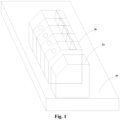
- Fig. 1 is a diagram of a power supplier with wireless communication module in related art. As shown in Fig. 1 , a wireless communication module 10 and multiple terminal modules 20 are placed on a substrate 30. The wireless communication module 10 is made into an independent component and placed on the edge of the substrate 30.
- the wireless communication module 10 is easily tilted to one side. When it tilts, it will affect the wireless communication function, and when it tilts outward, it will be easily hit by a shell of the power supplier.
- inventions are defined by a power supplier in accordance with claim 1. Further preferred embodiments are defined in the dependent claims.
- embodiments of the present disclosure provide a power supplier.
- a wireless communication module is spliced with a terminal module. Therefore, the wireless communication module of the power supplier will be more solid and will not be easy to tilt.
- a power supplier which includes: a substrate; at least one terminal module, configured to be placed on the substrate; and a wireless communication module, configured to be spliced with the terminal module when the terminal module and the wireless communication module are placed on the substrate.
- the terminal module comprises a connecting hole, which is configured to be connected to an electrical device and supply power to the electrical device.
- the wireless communication module has the same size as the terminal module.
- the terminal module and the wireless communication module are spliced together by using a first connecting structure.
- the first connecting structure includes: a first connecting part, configured to be placed on a first surface of the terminal module; a second connecting part, configured to be placed on a first surface of the wireless communication module, the first connecting part is any one of a first convex part and a first receiving hole, the second connecting part is the other one of the first convex part and the first receiving hole, the first convex part is received in the first receiving hole when the terminal module and the wireless communication module are spliced together.
- two adjacent terminal modules are spliced together by using a second connecting structure.
- the second connecting structure includes: a third connecting part, configured to be placed on a first surface of the terminal module; a fourth connecting part, configured to be placed on a second surface of the terminal module, the second surface is opposite the first surface, the third connecting part is any one of a second convex part and a second receiving hole, the fourth connecting part is the other one of the second convex part and the second receiving hole, the second convex part is received in the second receiving hole when two adjacent terminal modules are spliced together.
- the wireless communication module includes an antenna.
- the wireless communication module further includes a wireless communication controller which is integrated with the antenna.
- the terminal module includes a connecting pin
- the terminal module is placed on the substrate via the connecting pin.
- the terminal module includes a connecting hole, which is used to connect to an electrical device and supply power to the electrical device.
- a wireless communication module is spliced with a terminal module. Therefore, the wireless communication module of the power supplier will be more solid and will not be easy to tilt.
- the terms “first” and “second” refer to different elements.
- the singular forms “a” and “an” are intended to include the plural forms as well, unless the context clearly indicates otherwise.
- the terms “comprises,” “comprising,” “has,” “having,” “includes” and/or “including” as used herein, specify the presence of stated features, elements, and/or components and the like, but do not preclude the presence or addition of one or more other features, elements, components and/or combinations thereof.
- a power supplier is provided in a first embodiment.
- Fig. 2 is a diagram of a power supplier in accordance with an embodiment of the present disclosure.
- a power supplier 1 includes a substrate 11, at least one terminal module 12, and a wireless communication module 13.
- the terminal module 12 is placed on the substrate.
- the wireless communication module 13 is spliced with the terminal module 12. Therefore, the wireless communication module of the power supplier will be more solid and will not be easy to tilt.
- the wireless communication module 13 has the same size as the terminal module 12.
- the terminal module 12 and the wireless communication module 13 are spliced together by using a first connecting structure.
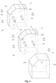
- Fig. 3 is a diagram of the terminal module and the wireless communication module in accordance with an embodiment of the present disclosure.
- the terminal module 12 includes a first surface S11.
- a first connecting part 121 is placed on the first surface S11.
- the wireless communication module 13 includes a first surface S21.
- a second connecting part 131 is placed on the first surface S21.
- the first connecting structure 14 includes the first connecting part 121 and the second connecting part 131.
- the first connecting part 121 may be any one of a first convex part and a first receiving hole
- the second connecting part 131 is the other one of the first convex part and the first receiving hole.
- the first convex part may be received in the first receiving hole when the terminal module 12 and the wireless communication module 13 are spliced together.
- the number of first connecting part 121 may be at least one, and the number of the second connecting part 131 may be at least one.
- function of the first connecting structure 14 is realized by mechanical connection of the first connecting part 121 and the second connecting part 131.
- the first connecting structure 14 may include magnetic parts, thus function of the first connecting structure 14 may be realized by magnetic attraction between the magnetic parts.
- two adjacent terminal modules 12 may be spliced together by using a second connecting structure. Therefore, the terminal modules 12 of the power supplier will be more solid and will not be easy to tilt
- a third connecting part 122 is placed on the first surface S11 the terminal module 12.
- the terminal module 12 further includes a second surface S12.
- a fourth connecting part 123 is placed on the second surface S12.
- the second connecting structure 15 includes the third connecting part 122 and the fourth connecting part 123.
- the third connecting part 122 may be any one of a second convex part and a second receiving hole
- the fourth connecting part 123 is the other one of the second convex part and the second receiving hole.
- the second convex part may be received in the second receiving hole when two adjacent terminal modules 12 are spliced together.
- the number of third connecting part 122 may be at least one, and the number of the fourth connecting part 123 may be at least one.
- the location and size of the third connecting part 122 may be different from the location and size of the first connecting part 121.
- the location and size of the third connecting part 122 may be the same as the location and size of the first connecting part 121, then, the first connecting part 121 may realize the function of the third connecting part 122 to connect with the fourth connecting part 123.
- function of the second connecting structure 15 is realized by mechanical connection of the third connecting part 122 and the fourth connecting part 123.
- the second connecting structure 15 may include magnetic parts, thus function of the second connecting structure 15 may be realized by magnetic attraction between the magnetic parts.
- the first surface S21 of the wireless communication module 13 may include a receiving part 131a which may receive the third connecting part 122 on the first surface S11 of the terminal module 12.
- the second surface S12 of the terminal module 12 may include a receiving part 123a which may receive the first connecting part 121 on the first surface S11 of the adjacent terminal module 12.
- the terminal module 12 may further include a connecting pin 124.
- the terminal module 12 may be placed on the substrate 11 via the connecting pin 124.
- the connecting pin 124 may provide mechanical and electrical connection between the terminal module 12 and the substrate 11.
- the terminal module 12 may further include a connecting hole 125.
- the connecting hole 125 may be used to connect to an electrical device and supply power to the electrical device.
- the electrical device may be a lighting device, for example, a LED (Light Emitting Diode) device.
- the wireless communication module 13 may communicate with other devices via wireless signals.
- the wireless communication module 13 may be near field communication (NFC) module.
- NFC near field communication
- the wireless communication module 13 may include an antenna, which is used to receive and transmit wireless signals.
- the wireless communication module 13 may further include a wireless communication controller which is integrated with the antenna.
- the wireless communication controller may perform digital or analogue process on the received and/or to be transmitted wireless signals.
- the wireless communication module 13 is spliced with the terminal module 12. Therefore, the wireless communication module of the power supplier will be more solid and will not be easy to tilt.
- the use of the wireless communication module 13 will be more flexible, as the wireless communication module 13 can be easily assembled or not assembled ith the terminal module 12.
- the wireless communication module 13 may be spliced with the terminal module 12 which is located outside of an iron shell of the power supplier, thus the interference of other components and the iron shell on wireless communication function will be prevented.
Landscapes
- Telephone Set Structure (AREA)
Description
- Embodiments of the present disclosure generally relate to the field of lighting, and more particularly, to a power supplier.
DocumentEP 2 334 155 A1 discloses a solid state lighting system. DocumentWO 2014/073913 A1 discloses a lighting apparatus having a communication module. DocumentUS 2016/0233605 A1 discloses a power control system. DocumentWO 2014/101824 A1 discloses a smart home system having a discrete circuit for an authentication and system management method. DocumentEP 3 125 371 A1 discloses a connector and a connector assembly. DocumentUS 2018/0054907 A1 discloses a multifunctional electronic product combining structure. DocumentCN 105789962 A discloses a modular extension socket with lock. - This section introduces aspects that may facilitate better understanding of the present disclosure. Accordingly, the statements of this section are to be read in this light and are not to be understood as admissions about what is in the prior art or what is not in the prior art.
- Nowadays, smart appliances are becoming more and more popular. The use of wireless communication is also becoming more common. Therefore, in the lighting industry, some lighting power sources add wireless communication functionality. The wireless communication may be Bluetooth communication, near field communication (NFC), etc.
-
Fig. 1 is a diagram of a power supplier with wireless communication module in related art. As shown inFig. 1 , awireless communication module 10 andmultiple terminal modules 20 are placed on asubstrate 30. Thewireless communication module 10 is made into an independent component and placed on the edge of thesubstrate 30. - Inventors of this disclosure found the following limitation in related art: the
wireless communication module 10 is easily tilted to one side. When it tilts, it will affect the wireless communication function, and when it tilts outward, it will be easily hit by a shell of the power supplier. - The invention is defined by a power supplier in accordance with
claim 1. Further preferred embodiments are defined in the dependent claims. In general, embodiments of the present disclosure provide a power supplier. In the embodiments, a wireless communication module is spliced with a terminal module. Therefore, the wireless communication module of the power supplier will be more solid and will not be easy to tilt. - In a first aspect, there is provided a power supplier, which includes: a substrate; at least one terminal module, configured to be placed on the substrate; and a wireless communication module, configured to be spliced with the terminal module when the terminal module and the wireless communication module are placed on the substrate. The terminal module comprises a connecting hole, which is configured to be connected to an electrical device and supply power to the electrical device.
- In an embodiment, the wireless communication module has the same size as the terminal module.
- In an embodiment, the terminal module and the wireless communication module are spliced together by using a first connecting structure.
- In an embodiment, the first connecting structure includes: a first connecting part, configured to be placed on a first surface of the terminal module; a second connecting part, configured to be placed on a first surface of the wireless communication module, the first connecting part is any one of a first convex part and a first receiving hole, the second connecting part is the other one of the first convex part and the first receiving hole, the first convex part is received in the first receiving hole when the terminal module and the wireless communication module are spliced together.
- In an embodiment, two adjacent terminal modules are spliced together by using a second connecting structure.
- In an embodiment, the second connecting structure includes: a third connecting part, configured to be placed on a first surface of the terminal module; a fourth connecting part, configured to be placed on a second surface of the terminal module, the second surface is opposite the first surface, the third connecting part is any one of a second convex part and a second receiving hole, the fourth connecting part is the other one of the second convex part and the second receiving hole, the second convex part is received in the second receiving hole when two adjacent terminal modules are spliced together.
- In an embodiment, the wireless communication module includes an antenna.
- In an embodiment, the wireless communication module further includes a wireless communication controller which is integrated with the antenna.
- In an embodiment, the terminal module includes a connecting pin,
- the terminal module is placed on the substrate via the connecting pin.
- The terminal module includes a connecting hole, which is used to connect to an electrical device and supply power to the electrical device.
- According to various embodiments of the present disclosure, a wireless communication module is spliced with a terminal module. Therefore, the wireless communication module of the power supplier will be more solid and will not be easy to tilt.
- The above and other aspects, features, and benefits of various embodiments of the disclosure will become more fully apparent, by way of example, from the following detailed description with reference to the accompanying drawings, in which like reference numerals or letters are used to designate like or equivalent elements. The drawings are illustrated for facilitating better understanding of the embodiments of the disclosure and not necessarily drawn to scale, in which:
-
Fig. 1 is a diagram of a power supplier with wireless communication module in related art; -
Fig. 2 is a diagram of a power supplier in accordance with an embodiment of the present disclosure; -
Fig. 3 is a diagram of the terminal module and the wireless communication module in accordance with an embodiment of the present disclosure. - The present disclosure will now be discussed with reference to several example embodiments. It should be understood that these embodiments are discussed only for the purpose of enabling those skilled persons in the art to better understand and thus implement the present disclosure, rather than suggesting any limitations on the scope of the present disclosure.
- As used herein, the terms "first" and "second" refer to different elements. The singular forms "a" and "an" are intended to include the plural forms as well, unless the context clearly indicates otherwise. The terms "comprises," "comprising," "has," "having," "includes" and/or "including" as used herein, specify the presence of stated features, elements, and/or components and the like, but do not preclude the presence or addition of one or more other features, elements, components and/or combinations thereof. The term "based on" is to be read as "based at least in part on." The term "one embodiment" and "an embodiment" are to be read as "at least one embodiment." The term "another embodiment" is to be read as "at least one other embodiment." Other definitions, explicit and implicit, may be included below.
- A power supplier is provided in a first embodiment.
-
Fig. 2 is a diagram of a power supplier in accordance with an embodiment of the present disclosure. As shown inFig. 2 , apower supplier 1 includes asubstrate 11, at least oneterminal module 12, and awireless communication module 13. - In the embodiment, the
terminal module 12 is placed on the substrate. Thewireless communication module 13 is spliced with theterminal module 12. Therefore, the wireless communication module of the power supplier will be more solid and will not be easy to tilt. - As shown in
Fig. 2 , thewireless communication module 13 has the same size as theterminal module 12. - In the embodiment, the
terminal module 12 and thewireless communication module 13 are spliced together by using a first connecting structure. -
Fig. 3 is a diagram of the terminal module and the wireless communication module in accordance with an embodiment of the present disclosure. - As shown in
Fig. 3 , theterminal module 12 includes a first surface S11. A first connectingpart 121 is placed on the first surface S11. Thewireless communication module 13 includes a first surface S21. A second connectingpart 131 is placed on the first surface S21. - In the embodiment, the first connecting
structure 14 includes the first connectingpart 121 and the second connectingpart 131. - In the embodiment, the first connecting
part 121 may be any one of a first convex part and a first receiving hole, and the second connectingpart 131 is the other one of the first convex part and the first receiving hole. The first convex part may be received in the first receiving hole when theterminal module 12 and thewireless communication module 13 are spliced together. - In the embodiment, the number of first connecting
part 121 may be at least one, and the number of the second connectingpart 131 may be at least one. - In the embodiment, function of the first connecting
structure 14 is realized by mechanical connection of the first connectingpart 121 and the second connectingpart 131. However, the embodiment will not be limited thereto, for example, the first connectingstructure 14 may include magnetic parts, thus function of the first connectingstructure 14 may be realized by magnetic attraction between the magnetic parts. - In the embodiment, two adjacent
terminal modules 12 may be spliced together by using a second connecting structure. Therefore, theterminal modules 12 of the power supplier will be more solid and will not be easy to tilt - As shown in
Fig. 3 a third connectingpart 122 is placed on the first surface S11 theterminal module 12. Theterminal module 12 further includes a second surface S12. A fourth connectingpart 123 is placed on the second surface S12. - In the embodiment, the second connecting
structure 15 includes the third connectingpart 122 and the fourth connectingpart 123. - In the embodiment, the third connecting
part 122 may be any one of a second convex part and a second receiving hole, and the fourth connectingpart 123 is the other one of the second convex part and the second receiving hole. The second convex part may be received in the second receiving hole when two adjacentterminal modules 12 are spliced together. - In the embodiment, the number of third connecting
part 122 may be at least one, and the number of the fourth connectingpart 123 may be at least one. - In one embodiment, the location and size of the third connecting
part 122 may be different from the location and size of the first connectingpart 121. - In another embodiment, the location and size of the third connecting
part 122 may be the same as the location and size of the first connectingpart 121, then, the first connectingpart 121 may realize the function of the third connectingpart 122 to connect with the fourth connectingpart 123. - In the embodiment, function of the second connecting
structure 15 is realized by mechanical connection of the third connectingpart 122 and the fourth connectingpart 123. However, the embodiment will not be limited thereto, for example, the second connectingstructure 15 may include magnetic parts, thus function of the second connectingstructure 15 may be realized by magnetic attraction between the magnetic parts. - As shown in
Fig. 3 , the first surface S21 of thewireless communication module 13 may include a receivingpart 131a which may receive the third connectingpart 122 on the first surface S11 of theterminal module 12. - The second surface S12 of the
terminal module 12 may include a receivingpart 123a which may receive the first connectingpart 121 on the first surface S11 of theadjacent terminal module 12. - In the embodiment, as shown in
Fig. 3 , theterminal module 12 may further include a connectingpin 124. Theterminal module 12 may be placed on thesubstrate 11 via the connectingpin 124. The connectingpin 124 may provide mechanical and electrical connection between theterminal module 12 and thesubstrate 11. - In the embodiment, as shown in
Fig. 3 , theterminal module 12 may further include a connectinghole 125. The connectinghole 125 may be used to connect to an electrical device and supply power to the electrical device. The electrical device may be a lighting device, for example, a LED (Light Emitting Diode) device. - In the embodiment, the
wireless communication module 13 may communicate with other devices via wireless signals. For example, thewireless communication module 13 may be near field communication (NFC) module. - In the embodiment, the
wireless communication module 13 may include an antenna, which is used to receive and transmit wireless signals. - In the embodiment, the
wireless communication module 13 may further include a wireless communication controller which is integrated with the antenna. The wireless communication controller may perform digital or analogue process on the received and/or to be transmitted wireless signals. - As can be seen from the above embodiments, the
wireless communication module 13 is spliced with theterminal module 12. Therefore, the wireless communication module of the power supplier will be more solid and will not be easy to tilt. The use of thewireless communication module 13 will be more flexible, as thewireless communication module 13 can be easily assembled or not assembled ith theterminal module 12. In some cases, thewireless communication module 13 may be spliced with theterminal module 12 which is located outside of an iron shell of the power supplier, thus the interference of other components and the iron shell on wireless communication function will be prevented. - Further, while operations are depicted in a particular order, this should not be understood as requiring that such operations be performed in the particular order shown or in sequential order, or that all illustrated operations be performed, to achieve desirable results. In certain circumstances, multitasking and parallel processing may be advantageous. Likewise, while several specific implementation details are contained in the above discussions, these should not be construed as limitations on the scope of the present disclosure, but rather as descriptions of features that may be specific to particular embodiments. The invention is defined by the appended claims.
- Although the present disclosure has been described in language specific to structural features and/or methodological acts, it is to be understood that the present disclosure defined in the appended claims is not necessarily limited to the specific features or acts described above. Rather, the specific features and acts described above are disclosed as example forms of implementing the claims.
Claims (9)
- A power supplier (1), comprising:a substrate (11);at least one terminal module (12), configured to be placed on the substrate (11), wherein the at least one terminal module (12) comprises a connecting hole (125) configured to be connected to an electrical device to thereby supply power to the electrical device,characterized in that the power supplier (1) further comprises:
a wireless communication module (13), configured to be spliced with the at least one terminal module (12) when the at least one terminal module (12) and the wireless communication module (13) are placed on the substrate (11). - The power supplier (1) according to claim 1, wherein the wireless communication module (13) has the same size as the at least one terminal module (12).
- The power supplier (1) according to claim 1, wherein the at least one terminal module (12) and the wireless communication module (13) are configured to be spliced together by a first connecting structure (14).
- The power supplier (1) according to claim 3, wherein the first connecting structure (14)
comprises:a first connecting part (121), configured to be placed on a first surface (S11) of the at least one terminal module (12);a second connecting part (131), configured to be placed on a first surface (S21) of the wireless communication module (13),the first connecting part (121) is any one of a first convex part and a first receiving hole,the second connecting part (131) is the other one of the first convex part and the first receiving hole,the first convex part is configured to be received in the first receiving hole when the at least one terminal module (12) and the wireless communication module (13) are spliced together. - The power supplier (1) according to claim 1, wherein the at least one terminal module (12) comprises two adjacent terminal modules (12) configured to be spliced together by a second connecting structure (15).
- The power supplier (1) according to claim 5, wherein, for each terminal module of the two adjacent terminal modules (12), the second connecting structure (15) comprises:a third connecting part (122), configured to be placed on a first surface (S 11) of the terminal module (12);a fourth connecting part (123), configured to be placed on a second surface (S12) of the terminal module (12),the second surface (S12) is opposite the first surface (S11),the third connecting part (122) is any one of a second convex part and a second receiving hole,the fourth connecting part (123) is the other one of the second convex part and the second receiving hole,wherein the second convex part of a first module of the two adjacent modules (12) is configured to be received in the second receiving hole a second module of the two adjacent modules (12) when the two adjacent terminal modules (12) are spliced together.
- The power supplier (1) according to claim 1, wherein
the wireless communication module (13) comprises an antenna. - The power supplier (1) according to claim 7, wherein
the wireless communication module (13) further comprises a wireless communication controller which is integrated with the antenna. - The power supplier (1) according to claim 1, whereinthe at least one terminal module (12) comprises a connecting pin (124),the at least one terminal module (12) is configured to be placed on the substrate (11) via the connecting pin (124).
Applications Claiming Priority (1)
| Application Number | Priority Date | Filing Date | Title |
|---|---|---|---|
| PCT/CN2018/081370 WO2019183929A1 (en) | 2018-03-30 | 2018-03-30 | Power supplier |
Publications (3)
| Publication Number | Publication Date |
|---|---|
| EP3756247A1 EP3756247A1 (en) | 2020-12-30 |
| EP3756247A4 EP3756247A4 (en) | 2021-09-08 |
| EP3756247B1 true EP3756247B1 (en) | 2024-09-04 |
Family
ID=68062095
Family Applications (1)
| Application Number | Title | Priority Date | Filing Date |
|---|---|---|---|
| EP18911511.6A Active EP3756247B1 (en) | 2018-03-30 | 2018-03-30 | Power supplier |
Country Status (3)
| Country | Link |
|---|---|
| EP (1) | EP3756247B1 (en) |
| CN (1) | CN111819737A (en) |
| WO (1) | WO2019183929A1 (en) |
Citations (3)
| Publication number | Priority date | Publication date | Assignee | Title |
|---|---|---|---|---|
| CN105789962A (en) * | 2016-04-19 | 2016-07-20 | 程雨佳 | Modular extension socket with lock |
| EP3125371A1 (en) * | 2015-07-31 | 2017-02-01 | Tyco Electronics (Shanghai) Co. Ltd. | Connector and connector assembly |
| US20180054907A1 (en) * | 2016-05-09 | 2018-02-22 | Qixuan ZHANG | Multifunctional Electronic Product Combining Structure |
Family Cites Families (15)
| Publication number | Priority date | Publication date | Assignee | Title |
|---|---|---|---|---|
| CN1301569C (en) * | 2001-03-09 | 2007-02-21 | 松下电工株式会社 | Wire connectors for printed circuit boards |
| US7753740B2 (en) * | 2007-07-20 | 2010-07-13 | Numatics, Incorporated | Modular electrical bus system |
| US8264852B2 (en) * | 2008-10-27 | 2012-09-11 | General Electric Company | Pluggable bases with different levels of redundancy and method for same |
| US8878454B2 (en) * | 2009-12-09 | 2014-11-04 | Tyco Electronics Corporation | Solid state lighting system |
| KR101999660B1 (en) * | 2012-11-08 | 2019-10-01 | 엘지이노텍 주식회사 | The lighting apparatus having the communication module |
| CN103092162B (en) | 2012-12-28 | 2016-03-16 | 东莞市傲思电子科技有限公司 | Split intelligent domestic system and the method for managing system of circuit authenticates |
| GB201316969D0 (en) * | 2013-09-26 | 2013-11-06 | Made In Mind Ltd | Power Supply System |
| CN203553526U (en) * | 2013-11-01 | 2014-04-16 | 福一开电气有限公司 | Socket assembly with wireless router function |
| JP2017514449A (en) * | 2014-02-14 | 2017-06-01 | ヤニー デロス | Modular electronics system to interface replaceable components |
| JP2015204294A (en) * | 2014-04-10 | 2015-11-16 | 生興 廖 | Wall socket having connector module and wall switch having connector module |
| US9640962B2 (en) | 2015-02-11 | 2017-05-02 | Molex, Llc | Power control system having modules |
| CN106507562A (en) * | 2016-09-30 | 2017-03-15 | 上海三思电子工程有限公司 | Smart lamps and their functional modules |
| CN206274558U (en) * | 2016-12-05 | 2017-06-23 | 郑维海 | A kind of modular indefinite extension Intelligent socket |
| CN111629504B (en) * | 2017-04-01 | 2023-02-03 | 广东易百珑智能科技有限公司 | Lighting system without wiring control lines and its application method |
| CN206893951U (en) * | 2017-06-14 | 2018-01-16 | 张国俊 | Track jack system and power track box, socket |
-
2018
- 2018-03-30 CN CN201880090924.1A patent/CN111819737A/en active Pending
- 2018-03-30 EP EP18911511.6A patent/EP3756247B1/en active Active
- 2018-03-30 WO PCT/CN2018/081370 patent/WO2019183929A1/en not_active Ceased
Patent Citations (3)
| Publication number | Priority date | Publication date | Assignee | Title |
|---|---|---|---|---|
| EP3125371A1 (en) * | 2015-07-31 | 2017-02-01 | Tyco Electronics (Shanghai) Co. Ltd. | Connector and connector assembly |
| CN105789962A (en) * | 2016-04-19 | 2016-07-20 | 程雨佳 | Modular extension socket with lock |
| US20180054907A1 (en) * | 2016-05-09 | 2018-02-22 | Qixuan ZHANG | Multifunctional Electronic Product Combining Structure |
Also Published As
| Publication number | Publication date |
|---|---|
| CN111819737A (en) | 2020-10-23 |
| WO2019183929A1 (en) | 2019-10-03 |
| EP3756247A1 (en) | 2020-12-30 |
| EP3756247A4 (en) | 2021-09-08 |
Similar Documents
| Publication | Publication Date | Title |
|---|---|---|
| KR20190019163A (en) | Driver system for light emitting device | |
| KR20190131167A (en) | Electronic device comprising antenna and method thereof | |
| EP2733686B1 (en) | Gateway system including communication module and method of driving the same | |
| US7862361B2 (en) | Electrical flex connector for mounting on a printed circuit board | |
| US11513784B2 (en) | Software update device and software update method using same | |
| EP1059688A3 (en) | Radio communication apparatus with retractable antenna and its impedance matching method | |
| MX2010000119A (en) | Antenna system for remote control automotive application. | |
| CN111164901B (en) | Near field communication device | |
| JP6659678B2 (en) | Supply cable, driver configuration with wireless control function, and control method | |
| CN1599287B (en) | Light receiving and emitting electronic apparatus | |
| US8463978B2 (en) | Computer with ability to charge electronic device in power off state and USB interface module thereof | |
| US9960501B2 (en) | Electronic device, communication device, and antenna gain enhancement method for a detachable wireless communication module | |
| EP1434159A3 (en) | Integrated antenna type non-contact IC card reader/writer | |
| WO2017117943A1 (en) | Mobile terminal and external antenna | |
| WO2019183929A1 (en) | Power supplier | |
| CN206878288U (en) | A kind of Internet of Things intelligent data line and system for possessing positioning monitor function | |
| US20220192023A1 (en) | Wireless communication board and electronic device having same | |
| KR20160001366U (en) | Wireless power charging apparatus | |
| WO2004062030A3 (en) | Antenna assembly with electrical connectors | |
| CN208240869U (en) | A kind of NFC antenna with diversity antenna common antenna cabling | |
| EP3573423B1 (en) | Securing an iot device at an access point device to avoid theft | |
| US6906670B2 (en) | Card device having antenna of two or more different frequencies | |
| US10158385B1 (en) | Holster providing antenna coverage | |
| EP4282230B1 (en) | A driver for lighting means | |
| KR102161732B1 (en) | Antenna apparatus |
Legal Events
| Date | Code | Title | Description |
|---|---|---|---|
| STAA | Information on the status of an ep patent application or granted ep patent |
Free format text: STATUS: THE INTERNATIONAL PUBLICATION HAS BEEN MADE |
|
| PUAI | Public reference made under article 153(3) epc to a published international application that has entered the european phase |
Free format text: ORIGINAL CODE: 0009012 |
|
| STAA | Information on the status of an ep patent application or granted ep patent |
Free format text: STATUS: REQUEST FOR EXAMINATION WAS MADE |
|
| 17P | Request for examination filed |
Effective date: 20200923 |
|
| AK | Designated contracting states |
Kind code of ref document: A1 Designated state(s): AL AT BE BG CH CY CZ DE DK EE ES FI FR GB GR HR HU IE IS IT LI LT LU LV MC MK MT NL NO PL PT RO RS SE SI SK SM TR |
|
| AX | Request for extension of the european patent |
Extension state: BA ME |
|
| RIN1 | Information on inventor provided before grant (corrected) |
Inventor name: HU, ZAOSHENG Inventor name: MIDDEL, TJACO Inventor name: ZHOU, CUI |
|
| RIN1 | Information on inventor provided before grant (corrected) |
Inventor name: MIDDEL, TJACO Inventor name: ZHOU, CUI Inventor name: HU, ZAOSHENG |
|
| DAV | Request for validation of the european patent (deleted) | ||
| DAX | Request for extension of the european patent (deleted) | ||
| A4 | Supplementary search report drawn up and despatched |
Effective date: 20210811 |
|
| RIC1 | Information provided on ipc code assigned before grant |
Ipc: H01R 13/66 20060101ALI20210805BHEP Ipc: H01R 13/514 20060101AFI20210805BHEP |
|
| STAA | Information on the status of an ep patent application or granted ep patent |
Free format text: STATUS: EXAMINATION IS IN PROGRESS |
|
| 17Q | First examination report despatched |
Effective date: 20230313 |
|
| GRAP | Despatch of communication of intention to grant a patent |
Free format text: ORIGINAL CODE: EPIDOSNIGR1 |
|
| STAA | Information on the status of an ep patent application or granted ep patent |
Free format text: STATUS: GRANT OF PATENT IS INTENDED |
|
| INTG | Intention to grant announced |
Effective date: 20240426 |
|
| GRAS | Grant fee paid |
Free format text: ORIGINAL CODE: EPIDOSNIGR3 |
|
| GRAA | (expected) grant |
Free format text: ORIGINAL CODE: 0009210 |
|
| STAA | Information on the status of an ep patent application or granted ep patent |
Free format text: STATUS: THE PATENT HAS BEEN GRANTED |
|
| AK | Designated contracting states |
Kind code of ref document: B1 Designated state(s): AL AT BE BG CH CY CZ DE DK EE ES FI FR GB GR HR HU IE IS IT LI LT LU LV MC MK MT NL NO PL PT RO RS SE SI SK SM TR |
|
| P01 | Opt-out of the competence of the unified patent court (upc) registered |
Free format text: CASE NUMBER: APP_44202/2024 Effective date: 20240730 |
|
| REG | Reference to a national code |
Ref country code: GB Ref legal event code: FG4D |
|
| REG | Reference to a national code |
Ref country code: CH Ref legal event code: EP |
|
| REG | Reference to a national code |
Ref country code: IE Ref legal event code: FG4D |
|
| REG | Reference to a national code |
Ref country code: DE Ref legal event code: R096 Ref document number: 602018074126 Country of ref document: DE |
|
| REG | Reference to a national code |
Ref country code: DE Ref legal event code: R084 Ref document number: 602018074126 Country of ref document: DE |
|
| REG | Reference to a national code |
Ref country code: LT Ref legal event code: MG9D |
|
| REG | Reference to a national code |
Ref country code: NL Ref legal event code: MP Effective date: 20240904 |
|
| PG25 | Lapsed in a contracting state [announced via postgrant information from national office to epo] |
Ref country code: NO Free format text: LAPSE BECAUSE OF FAILURE TO SUBMIT A TRANSLATION OF THE DESCRIPTION OR TO PAY THE FEE WITHIN THE PRESCRIBED TIME-LIMIT Effective date: 20241204 |
|
| PG25 | Lapsed in a contracting state [announced via postgrant information from national office to epo] |
Ref country code: GR Free format text: LAPSE BECAUSE OF FAILURE TO SUBMIT A TRANSLATION OF THE DESCRIPTION OR TO PAY THE FEE WITHIN THE PRESCRIBED TIME-LIMIT Effective date: 20241205 Ref country code: FI Free format text: LAPSE BECAUSE OF FAILURE TO SUBMIT A TRANSLATION OF THE DESCRIPTION OR TO PAY THE FEE WITHIN THE PRESCRIBED TIME-LIMIT Effective date: 20240904 Ref country code: PL Free format text: LAPSE BECAUSE OF FAILURE TO SUBMIT A TRANSLATION OF THE DESCRIPTION OR TO PAY THE FEE WITHIN THE PRESCRIBED TIME-LIMIT Effective date: 20240904 |
|
| PG25 | Lapsed in a contracting state [announced via postgrant information from national office to epo] |
Ref country code: BG Free format text: LAPSE BECAUSE OF FAILURE TO SUBMIT A TRANSLATION OF THE DESCRIPTION OR TO PAY THE FEE WITHIN THE PRESCRIBED TIME-LIMIT Effective date: 20240904 |
|
| PG25 | Lapsed in a contracting state [announced via postgrant information from national office to epo] |
Ref country code: LV Free format text: LAPSE BECAUSE OF FAILURE TO SUBMIT A TRANSLATION OF THE DESCRIPTION OR TO PAY THE FEE WITHIN THE PRESCRIBED TIME-LIMIT Effective date: 20240904 |
|
| PG25 | Lapsed in a contracting state [announced via postgrant information from national office to epo] |
Ref country code: HR Free format text: LAPSE BECAUSE OF FAILURE TO SUBMIT A TRANSLATION OF THE DESCRIPTION OR TO PAY THE FEE WITHIN THE PRESCRIBED TIME-LIMIT Effective date: 20240904 |
|
| PG25 | Lapsed in a contracting state [announced via postgrant information from national office to epo] |
Ref country code: RS Free format text: LAPSE BECAUSE OF FAILURE TO SUBMIT A TRANSLATION OF THE DESCRIPTION OR TO PAY THE FEE WITHIN THE PRESCRIBED TIME-LIMIT Effective date: 20241204 Ref country code: ES Free format text: LAPSE BECAUSE OF FAILURE TO SUBMIT A TRANSLATION OF THE DESCRIPTION OR TO PAY THE FEE WITHIN THE PRESCRIBED TIME-LIMIT Effective date: 20240904 |
|
| PG25 | Lapsed in a contracting state [announced via postgrant information from national office to epo] |
Ref country code: RS Free format text: LAPSE BECAUSE OF FAILURE TO SUBMIT A TRANSLATION OF THE DESCRIPTION OR TO PAY THE FEE WITHIN THE PRESCRIBED TIME-LIMIT Effective date: 20241204 Ref country code: PL Free format text: LAPSE BECAUSE OF FAILURE TO SUBMIT A TRANSLATION OF THE DESCRIPTION OR TO PAY THE FEE WITHIN THE PRESCRIBED TIME-LIMIT Effective date: 20240904 Ref country code: NO Free format text: LAPSE BECAUSE OF FAILURE TO SUBMIT A TRANSLATION OF THE DESCRIPTION OR TO PAY THE FEE WITHIN THE PRESCRIBED TIME-LIMIT Effective date: 20241204 Ref country code: LV Free format text: LAPSE BECAUSE OF FAILURE TO SUBMIT A TRANSLATION OF THE DESCRIPTION OR TO PAY THE FEE WITHIN THE PRESCRIBED TIME-LIMIT Effective date: 20240904 Ref country code: HR Free format text: LAPSE BECAUSE OF FAILURE TO SUBMIT A TRANSLATION OF THE DESCRIPTION OR TO PAY THE FEE WITHIN THE PRESCRIBED TIME-LIMIT Effective date: 20240904 Ref country code: GR Free format text: LAPSE BECAUSE OF FAILURE TO SUBMIT A TRANSLATION OF THE DESCRIPTION OR TO PAY THE FEE WITHIN THE PRESCRIBED TIME-LIMIT Effective date: 20241205 Ref country code: FI Free format text: LAPSE BECAUSE OF FAILURE TO SUBMIT A TRANSLATION OF THE DESCRIPTION OR TO PAY THE FEE WITHIN THE PRESCRIBED TIME-LIMIT Effective date: 20240904 Ref country code: ES Free format text: LAPSE BECAUSE OF FAILURE TO SUBMIT A TRANSLATION OF THE DESCRIPTION OR TO PAY THE FEE WITHIN THE PRESCRIBED TIME-LIMIT Effective date: 20240904 Ref country code: BG Free format text: LAPSE BECAUSE OF FAILURE TO SUBMIT A TRANSLATION OF THE DESCRIPTION OR TO PAY THE FEE WITHIN THE PRESCRIBED TIME-LIMIT Effective date: 20240904 |
|
| REG | Reference to a national code |
Ref country code: AT Ref legal event code: MK05 Ref document number: 1721408 Country of ref document: AT Kind code of ref document: T Effective date: 20240904 |
|
| PG25 | Lapsed in a contracting state [announced via postgrant information from national office to epo] |
Ref country code: NL Free format text: LAPSE BECAUSE OF FAILURE TO SUBMIT A TRANSLATION OF THE DESCRIPTION OR TO PAY THE FEE WITHIN THE PRESCRIBED TIME-LIMIT Effective date: 20240904 |
|
| PG25 | Lapsed in a contracting state [announced via postgrant information from national office to epo] |
Ref country code: IS Free format text: LAPSE BECAUSE OF FAILURE TO SUBMIT A TRANSLATION OF THE DESCRIPTION OR TO PAY THE FEE WITHIN THE PRESCRIBED TIME-LIMIT Effective date: 20250104 Ref country code: PT Free format text: LAPSE BECAUSE OF FAILURE TO SUBMIT A TRANSLATION OF THE DESCRIPTION OR TO PAY THE FEE WITHIN THE PRESCRIBED TIME-LIMIT Effective date: 20250106 |
|
| PG25 | Lapsed in a contracting state [announced via postgrant information from national office to epo] |
Ref country code: SM Free format text: LAPSE BECAUSE OF FAILURE TO SUBMIT A TRANSLATION OF THE DESCRIPTION OR TO PAY THE FEE WITHIN THE PRESCRIBED TIME-LIMIT Effective date: 20240904 Ref country code: RO Free format text: LAPSE BECAUSE OF FAILURE TO SUBMIT A TRANSLATION OF THE DESCRIPTION OR TO PAY THE FEE WITHIN THE PRESCRIBED TIME-LIMIT Effective date: 20240904 |
|
| PG25 | Lapsed in a contracting state [announced via postgrant information from national office to epo] |
Ref country code: EE Free format text: LAPSE BECAUSE OF FAILURE TO SUBMIT A TRANSLATION OF THE DESCRIPTION OR TO PAY THE FEE WITHIN THE PRESCRIBED TIME-LIMIT Effective date: 20240904 Ref country code: AT Free format text: LAPSE BECAUSE OF FAILURE TO SUBMIT A TRANSLATION OF THE DESCRIPTION OR TO PAY THE FEE WITHIN THE PRESCRIBED TIME-LIMIT Effective date: 20240904 |
|
| PG25 | Lapsed in a contracting state [announced via postgrant information from national office to epo] |
Ref country code: CZ Free format text: LAPSE BECAUSE OF FAILURE TO SUBMIT A TRANSLATION OF THE DESCRIPTION OR TO PAY THE FEE WITHIN THE PRESCRIBED TIME-LIMIT Effective date: 20240904 |
|
| PG25 | Lapsed in a contracting state [announced via postgrant information from national office to epo] |
Ref country code: SK Free format text: LAPSE BECAUSE OF FAILURE TO SUBMIT A TRANSLATION OF THE DESCRIPTION OR TO PAY THE FEE WITHIN THE PRESCRIBED TIME-LIMIT Effective date: 20240904 Ref country code: IT Free format text: LAPSE BECAUSE OF FAILURE TO SUBMIT A TRANSLATION OF THE DESCRIPTION OR TO PAY THE FEE WITHIN THE PRESCRIBED TIME-LIMIT Effective date: 20240904 |
|
| REG | Reference to a national code |
Ref country code: DE Ref legal event code: R097 Ref document number: 602018074126 Country of ref document: DE |
|
| PG25 | Lapsed in a contracting state [announced via postgrant information from national office to epo] |
Ref country code: DK Free format text: LAPSE BECAUSE OF FAILURE TO SUBMIT A TRANSLATION OF THE DESCRIPTION OR TO PAY THE FEE WITHIN THE PRESCRIBED TIME-LIMIT Effective date: 20240904 |
|
| PLBE | No opposition filed within time limit |
Free format text: ORIGINAL CODE: 0009261 |
|
| STAA | Information on the status of an ep patent application or granted ep patent |
Free format text: STATUS: NO OPPOSITION FILED WITHIN TIME LIMIT |
|
| 26N | No opposition filed |
Effective date: 20250605 |
|
| PG25 | Lapsed in a contracting state [announced via postgrant information from national office to epo] |
Ref country code: SE Free format text: LAPSE BECAUSE OF FAILURE TO SUBMIT A TRANSLATION OF THE DESCRIPTION OR TO PAY THE FEE WITHIN THE PRESCRIBED TIME-LIMIT Effective date: 20240904 |
|
| PG25 | Lapsed in a contracting state [announced via postgrant information from national office to epo] |
Ref country code: MC Free format text: LAPSE BECAUSE OF FAILURE TO SUBMIT A TRANSLATION OF THE DESCRIPTION OR TO PAY THE FEE WITHIN THE PRESCRIBED TIME-LIMIT Effective date: 20240904 |
|
| REG | Reference to a national code |
Ref country code: CH Ref legal event code: H13 Free format text: ST27 STATUS EVENT CODE: U-0-0-H10-H13 (AS PROVIDED BY THE NATIONAL OFFICE) Effective date: 20251023 |
|
| PG25 | Lapsed in a contracting state [announced via postgrant information from national office to epo] |
Ref country code: LU Free format text: LAPSE BECAUSE OF NON-PAYMENT OF DUE FEES Effective date: 20250330 |
|
| REG | Reference to a national code |
Ref country code: BE Ref legal event code: MM Effective date: 20250331 |
|
| PG25 | Lapsed in a contracting state [announced via postgrant information from national office to epo] |
Ref country code: BE Free format text: LAPSE BECAUSE OF NON-PAYMENT OF DUE FEES Effective date: 20250331 |
|
| PG25 | Lapsed in a contracting state [announced via postgrant information from national office to epo] |
Ref country code: CH Free format text: LAPSE BECAUSE OF NON-PAYMENT OF DUE FEES Effective date: 20250331 |
|
| PG25 | Lapsed in a contracting state [announced via postgrant information from national office to epo] |
Ref country code: IE Free format text: LAPSE BECAUSE OF NON-PAYMENT OF DUE FEES Effective date: 20250330 |
|
| PGFP | Annual fee paid to national office [announced via postgrant information from national office to epo] |
Ref country code: GB Payment date: 20260323 Year of fee payment: 9 |
|
| PGFP | Annual fee paid to national office [announced via postgrant information from national office to epo] |
Ref country code: DE Payment date: 20260320 Year of fee payment: 9 |
|
| PGFP | Annual fee paid to national office [announced via postgrant information from national office to epo] |
Ref country code: FR Payment date: 20260323 Year of fee payment: 9 |