EP3754921A1 - Pwm signaling and encoding multiple statuses - Google Patents
Pwm signaling and encoding multiple statuses Download PDFInfo
- Publication number
- EP3754921A1 EP3754921A1 EP19210124.4A EP19210124A EP3754921A1 EP 3754921 A1 EP3754921 A1 EP 3754921A1 EP 19210124 A EP19210124 A EP 19210124A EP 3754921 A1 EP3754921 A1 EP 3754921A1
- Authority
- EP
- European Patent Office
- Prior art keywords
- bit
- command input
- hardware
- state
- pulse width
- Prior art date
- Legal status (The legal status is an assumption and is not a legal conclusion. Google has not performed a legal analysis and makes no representation as to the accuracy of the status listed.)
- Granted
Links
Images



Classifications
-
- H—ELECTRICITY
- H04—ELECTRIC COMMUNICATION TECHNIQUE
- H04L—TRANSMISSION OF DIGITAL INFORMATION, e.g. TELEGRAPHIC COMMUNICATION
- H04L25/00—Baseband systems
- H04L25/38—Synchronous or start-stop systems, e.g. for Baudot code
- H04L25/40—Transmitting circuits; Receiving circuits
- H04L25/49—Transmitting circuits; Receiving circuits using code conversion at the transmitter; using predistortion; using insertion of idle bits for obtaining a desired frequency spectrum; using three or more amplitude levels ; Baseband coding techniques specific to data transmission systems
- H04L25/4902—Pulse width modulation; Pulse position modulation
-
- G—PHYSICS
- G05—CONTROLLING; REGULATING
- G05B—CONTROL OR REGULATING SYSTEMS IN GENERAL; FUNCTIONAL ELEMENTS OF SUCH SYSTEMS; MONITORING OR TESTING ARRANGEMENTS FOR SUCH SYSTEMS OR ELEMENTS
- G05B19/00—Program-control systems
- G05B19/02—Program-control systems electric
- G05B19/04—Program control other than numerical control, i.e. in sequence controllers or logic controllers
- G05B19/045—Program control other than numerical control, i.e. in sequence controllers or logic controllers using logic state machines, consisting only of a memory or a programmable logic device containing the logic for the controlled machine and in which the state of its outputs is dependent on the state of its inputs or part of its own output states, e.g. binary decision controllers, finite state controllers
-
- G—PHYSICS
- G05—CONTROLLING; REGULATING
- G05B—CONTROL OR REGULATING SYSTEMS IN GENERAL; FUNCTIONAL ELEMENTS OF SUCH SYSTEMS; MONITORING OR TESTING ARRANGEMENTS FOR SUCH SYSTEMS OR ELEMENTS
- G05B19/00—Program-control systems
- G05B19/02—Program-control systems electric
- G05B19/04—Program control other than numerical control, i.e. in sequence controllers or logic controllers
- G05B19/05—Programmable logic controllers, e.g. simulating logic interconnections of signals according to ladder diagrams or function charts
- G05B19/054—Input/output
-
- G—PHYSICS
- G06—COMPUTING OR CALCULATING; COUNTING
- G06F—ELECTRIC DIGITAL DATA PROCESSING
- G06F7/00—Methods or arrangements for processing data by operating upon the order or content of the data handled
- G06F7/38—Methods or arrangements for performing computations using exclusively denominational number representation, e.g. using binary, ternary, decimal representation
- G06F7/48—Methods or arrangements for performing computations using exclusively denominational number representation, e.g. using binary, ternary, decimal representation using non-contact-making devices, e.g. tube, solid state device; using unspecified devices
- G06F7/57—Arithmetic logic units [ALU], i.e. arrangements or devices for performing two or more of the operations covered by groups G06F7/483 – G06F7/556 or for performing logical operations
- G06F7/575—Basic arithmetic logic units, i.e. devices selectable to perform either addition, subtraction or one of several logical operations, using, at least partially, the same circuitry
-
- H—ELECTRICITY
- H03—ELECTRONIC CIRCUITRY
- H03K—PULSE TECHNIQUE
- H03K7/00—Modulating pulses with a continuously-variable modulating signal
- H03K7/08—Duration or width modulation ; Duty cycle modulation
Definitions
- the present disclosure relates generally to data transmission, and in particular, to the transmission of system status using pulse width modulation.
- Pulse width modulation can be used to signal the status of a hardware component in an aircraft, where a high degree of signal reliability is preferable.
- a first PWM duty cycle can be used to indicate that a sensor is available
- a second PWM duty cycle can be used to indicate that the sensor is unavailable, or severed.
- a PWM signaling scheme can be used to provide a two-state status of a particular hardware component. In some settings, it could be beneficial to signal one or more statuses in addition to providing a two-state status of a particular hardware component.
- a pulse width modulation signaling system includes a first control channel that is configured to receive a hardware Boolean command input from a first hardware status monitor, receive a software multi-bit command input from a first software system, and generate a first pulse width modulated signal that is representative of the Boolean command input and the software multi-bit command input.
- the hardware Boolean command input is a binary value of either a first state or a second state
- the software multi-bit command input comprises a binary value of either a first state or a second state
- the first pulse width modulated signal defines a duty cycle.
- a method for using a modulation signaling system that includes a first control channel for generating a first pulse width modulated signal that is representative of a Boolean command input and a software multi-bit command input includes receiving a hardware Boolean command input from a first hardware status monitor, receiving a software multi-bit command input from a first software system, and generating the first pulse width modulated signal.
- the hardware Boolean command input is a binary value of either a first state or a second state
- the software multi-bit command input comprises a binary value of either a first state or a second state
- the first pulse width modulated signal defines a duty cycle.
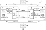
- FIG. 1 is schematic diagram of a multi-bit pulse width modulation signaling system.
- FIG. 2 is schematic diagram of a multi-bit logic channel for the multi-bit pulse width modulation signaling system shown in FIG. 1 .
- PWM pulse width modulation
- Shown in FIGS. 1 - 2 are pulse width modulation (PWM) signaling system 100, first control channel 120, first logic channel 122, multi-bit duty cycle selection logic circuit 123, software multi-bit command input 124, first software system 126, hardware Boolean command input 128, multi-bit duty cycle selection logic circuit output 129, first health status monitor 130, amplifier 131, first channel PWM output 132, first PWM signal 134, first channel PWM input 136, second PWM signal 138, second control channel 150, second logic channel 152, software multi-bit signal 154, second software system 156, hardware Boolean status signal 158, second health status monitor 160, second channel PWM input 162, second channel PWM output 166, aircraft sensors 170, aircraft sensors first channel feedback
- First control channel 120 can be used for signaling the status of a hardware component on an aircraft (not shown), while also signaling multiple software-detected statuses of the associated hardware component.
- a computer is a non-limiting example of a hardware component.
- the hardware status can be unsevered (i.e., connected, available) or severed (i.e., disconnected, unavailable).
- Non-limiting examples of software-detected statuses of the associated hardware component include performance level (e.g., degraded or non-degraded) and synchronism (i.e., sync) status (e.g., sync or non-sync).
- First control channel 120 includes first logic channel 122 which receives software multi-bit command input 124 from first software system 126, and hardware Boolean command input 128 from first health status monitor 130.
- First logic channel 122 includes multi-bit duty cycle selection logic circuit 123 (shown in FIG. 3 ), which receives software multi-bit command input 124 and hardware Boolean command input 128.
- First logic channel 122 provides multi-bit duty cycle selection logic circuit output 129 to amplifier 131, which in turn provides first channel PWM output 132.
- Multi-bit duty cycle selection logic circuit 123 operates as a pulse frequency of about 5,000 Hz. In some embodiments, the pulse frequency can range from about 4,000 - 6,000 Hz. In other embodiments, the pulse frequency can range from about 500 - 20,000 Hz.
- Amplifier 131 provides first channel PWM output 132 at a voltage level of about ⁇ 6 volts peak-to-peak.
- the voltage level of first channel PWM output 132 can range from about ⁇ 2 volts peak-to-peak to about ⁇ 6 volts peak-to-peak. In other embodiments, the voltage level of first channel PWM output 132 can be outside of these exemplary ranges.
- hardware Boolean command input 128 is representative of the severed/unsevered status of the hardware component.
- hardware Boolean command input 128 of 0 indicates the associated hardware component is unsevered (i.e., connected, available)
- hardware Boolean command input 128 of 1 indicates the associated hardware component is severed (i.e., disconnected, unavailable).
- the respective values of 0 and 1 can be referred to as binary values, or as a first state and second state, respectively.
- Software multi-bit command input 124 is a multi-bit word (i.e., binary word) that is received from first software system 126.
- software multi-bit command input 124 is a two-bit word, with the first indicative of the hardware system performance level (e.g., degraded or non-degraded), and the second bit indicative of the hardware sync status (e.g., sync or non-sync).
- bits in a multi-bit word are referred to in the order as presented from left to right.
- First control channel 120 provides first PWM signal 134 from first channel PWM output 132.
- First control channel 120 also receives second PWM signal 138 at first channel PWM input 136.
- Second control channel 150 receives first PWM signal 134 at second channel PWM input 162.
- Second control channel 150 includes second logic channel 152 which decodes first PWM signal 134 to provide software multi-bit signal 154 to second software system 156, and to provide hardware Boolean status signal 158 to second health status monitor 160.
- Second control channel 150 also provides second PWM signal from second channel PWM output 166.
- first channel 120 and second channel 150 continuously exchange the status information contained in PWM signals 134, 138 to ensure that first channel 120 and second channel 150 are each aware of the operational status of the other.
- first channel 120 and second channel 150 can provide adjustments to their respective control algorithms to maintain appropriate control of aircraft effectors 180.
- first channel 120 and second channel 150 can exchange status information periodically (i.e., non-continuously).
- first channel 120 and second channel 150 can operate independently, without exchanging status information.
- aircraft sensors 170 are various sensors that provide control algorithm feedback information that is used in calculating control commands 176, 178, to be provided to aircraft effectors 180.
- aircraft sensors include air data (e.g., airspeed, altitude, angle of attack), temperature (e.g., thermocouple, resistance temperature detector), and position sensors (e.g., linear variable differential transformer, rotary variable differential transformer).
- First and second health status monitors 130, 160 each represent independent circuitry that monitors the health of the control channel's ability to properly process feedback 172, 174 and develop correct control commands, 176, 178.
- elements that are part of this logic include watchdog timers, clock monitors, or other built-in-test circuitry that confirms the channel is capable of properly operating.
- the role of this function is to provide and independent element that forces a channel into a sever (i.e., disconnect) state if a fault is detected within the respective first or second control channel 120, 150 that prevents the proper generation of control commands 176, 178.
- Aircraft effectors 180 are various effectors (i.e., active elements, actuators) that can alter a state of a system in response to a command (e.g., control commands 176, 178).
- aircraft effectors 180 are commanded by control commands 176, 178 that are produced by the respective first or second control channel 120, 150 to position a flight control surface in an orientation that complies with the command (i.e., thereby achieving the desired aircraft orientation).
- Non-limiting examples of aircraft effectors 180 include hydraulic actuators and servo motors that position control surfaces on an aircraft wing.
- PWM signaling system 100 can include one or more processors (not shown in FIGS. 2 - 3 ) that are configured to implement functionality and/or process instructions for execution within PWM signaling system 100.
- the one or more prognostic processor(s) can be capable of processing instructions stored in one or more storage device(s) (not shown in FIGS. 2 - 3 ).
- Examples of processor(s) can include any one or more of a microprocessor, a controller, a digital signal processor (DSP), an application specific integrated circuit (ASIC), a field-programmable gate array (FPGA), or other equivalent discrete or integrated logic circuitry.
- DSP digital signal processor
- ASIC application specific integrated circuit
- FPGA field-programmable gate array
- PWM signaling system 100 can utilize data and signal analysis processing techniques different from and/or in addition to those described herein.
- PWM signaling system 100 can include only first control channel 120 that is configured to receive software multi-bit command input 124 and hardware Boolean command input 128, and to provide first PWM signal 134.
- PWM signaling system 100 can be configured to provide PWM signaling of hardware and multi-bit software command status to an external system.
- FIG. 3 is a second embodiment of a control channel for the multi-bit pulse width modulation signaling system shown in FIG. 1 . Shown in FIG. 3 are first PWM signal 134, second PWM signal 138, aircraft sensors first channel feedback 172, first channel control commands 176, first control channel 220, first logic channel 222, software multi-bit command input 224, first software system 226, hardware Boolean command input 228, independent health status monitor 230, first channel PWM output 232, first channel PWM input 236, acquisition circuitry 240, feedback data 241, first health status signal 242, second health status signal 244, command data 245, output circuitry 246, and third health status signal 248.
- first PWM signal 134, second PWM signal 138, aircraft sensors first channel feedback 172, and first channel control commands 176 are as provided above in regard to FIGS. 1 - 2 .
- the descriptions of first logic channel 222, software multi-bit command input 224, first software system 226, hardware Boolean command input 228, first health status monitor 230, first channel PWM output 232, and first channel PWM input 236 are substantially as provided above in regard to FIGS. 1 - 2 .
- Acquisition circuitry 240 acquires and processes aircraft sensors first channel feedback 172 to produce feedback data 241 and first health status signal 242.
- acquisition circuitry 240 can include analog-to-digital converter (ADC) circuits that digitize analog signals contained in aircraft sensors first channel feedback 172.
- ADC analog-to-digital converter
- Feedback data 241 are provided to first software system 226, which produces software multi-bit command input 224 (i.e., as described above in regard to FIGS. 1 - 2 ).
- First software system 226 also produces second health status signal 244 and command data 245.
- Command data 245 are provided to output circuitry 246, which in turn produces first channel control commands 176.
- Output circuitry 246 also produces third health status signal 248.
- First health status signal 242, second health status signal 244, and third health status signal 248, each being representative of various health status indications that are processed within first control channel 220, are all provided to first health status monitor 230.
- first health status monitor 230 calculates hardware Boolean command input 228, which is provided to first logic channel 222 (i.e., as described above).
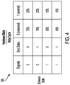
- FIG. 4 is a multi-bit duty cycle table using two bits for multi-bit pulse width modulation signaling system 100 shown in FIG. 1 .
- Shown in FIG. 4 is two-bit duty cycle state table 290, which can be used to describe first PWM signal 134 (shown in FIGS. 1 and 3 ), in an exemplary condition as follows.
- the first (i.e., left-most) bit represents a degraded (i.e., degrade) status, notifying the other (i.e., remote) remote channel(s) when the control channel is commanding aircraft effectors at a reduced level of effectiveness.
- degrade true (i.e., 0)
- a hardware Boolean command is true (i.e., 0, unsevered.
- a degrade status can be indicative of one or more non-critical fault conditions.
- the second (i.e., second left-most) bit) represents a synchronization (i.e., synchronized, sync) status between first and second control channels 120, 150.
- the first (i.e., left-most) bit can also be referred to as the most significant bit (MSB).
- MSB most significant bit
- LSB least-significant bit
- PWM duty cycle is either 75% or 25%, corresponding to a hardware state of unsevered or severed, respectively. This can be referred to as an unmodified PWM duty cycle. It is beneficial to convey additional information to other channels in conjunction with the sever state, particularly in the "unsevered" state. As an example, it is beneficial at the system level to indicate that a channel is unsevered, but not synchronized to the other channel(s). This would allow the remote channel(s) to adjust error detection mechanisms to a wider range to accommodate the lack of synchronization between channels. Additional information that is beneficial in PWM signaling system 100 is the status of flight control mode.
- first and second logic channels 122, 152 are capable of providing a PWM signal that is accurate to ⁇ 0.5 percentage points (%p). Accordingly, a PWM duty cycle that is rounded to the nearest whole-integer percentage point (%p) can be referred to as being approximately equal to a particular PWM duty cycle.
- first PWM signal 134 has a PWM duty cycle that ranges from 59.5 - 60.5%
- first PWM signal 134 can be said to have a PWM duty approximately equal to 60%, thereby representing a hardware state of 0 (i.e., unsevered), and a two-bit software state of 11 (i.e., degraded and synchronized).
- first PWM signal 134 has a PWM duty cycle that is outside of the tolerance range of +0.5 percentage points (%p)
- the PWM duty cycle tolerance range can be either narrower (i.e., tighter) or wider (i.e., looser) than +0.5 %p.
- the PWM duty cycle tolerance range can be +2 %p. Accordingly, in this second exemplary embodiment, if first PWM signal 134 has a PWM duty cycle that ranges from 58 - 62%, then first PWM signal 134 can be said to have a PWM duty approximately equal to 60%. It is to be appreciated that the PWM duty cycle tolerance in a particular embodiment of PWM signaling system 100 can be arbitrarily established by the designer based on several possible design considerations. For example, the electronic components and circuitry used in a particular embodiment can be a design consideration. It is also to be appreciated that the PWM duty cycle tolerance, and particularly, the maximum tolerance range, can be a function of the number of bits used in software multi-bit command input 124, and accordingly, the corresponding number different PWM duty cycle levels.
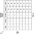
- FIG. 5 is multi-bit duty cycle table using three bits for a second embodiment of control channel 220 shown in FIG. 3 .
- Shown in FIG. 5 is three-bit duty cycle state table 292, which can be used to describe first PWM signal 134 in signaling three exemplary software states as follows.
- the first (i.e., left-most) bit represents degraded (i.e., degrade) status
- the second (i.e., second left-most) bit represents synchronism (i.e., sync) status
- the third (i.e., third left-most) bit represents autonomous (i.e., "auton") mode operation.
- Degraded and sync status are substantially similar to those described above in regard to FIG.
- Autonomous status can be representative of a representative of a flight control mode (e.g., autonomous flight control mode or direct flight control mode.
- various bits of software multi-bit command input 124 can be representative of other software-detected conditions, with non-limiting examples including various equipment condition flags relating to the performance of a built-in test, whether the equipment is on the ground or in the air, whether an equipment temperature is exceeding a particular limit, and whether or not external feedback data are being properly received.
- more than three bits can be used in software multi-bit command input 124 and therefore be encoded in first and/or second PWM signals 134, 138, with all numbers of bits being within the scope of the present disclosure.
- a tighter PWM duty cycle tolerance band can be typically associated with a greater number of bits. Accordingly, in a practical embodiment, any number of bits can be used within the ability of the associated electronic components and circuitry that encode and decode PWM signals.
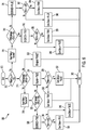
- FIG. 6 is a process flow diagram for the multi-bit pulse width modulation signaling system shown in FIG. 3 .
- first control channel 120 can be characterized stepping through two-bit duty cycle process flow chart 300. Beginning at start step 300, a series of decisions are made based on the received PWM duty cycle, thereby establishing the value of various conditions associated with hardware Boolean status (i.e., severed or unsevered), and with various software status flags associated with each bit of software multi-bit command input 124 (e.g., degrade status, sync status). It is to be appreciated that first control channel 120 and second control channel 150 each independently perform two-bit duty cycle process flow chart 300 to decode corresponding second PWM signal 138 and first PWM signal 134, respectively, while exchanging data with the other as described above in regard to FIGS. 1 and 4 .
- first and second control channels 120, 150 can periodically perform two-bit duty cycle process flow chart 300 by beginning again at start step 310.
- a timing signal i.e., clock pulse
- first and/or second control channels 120, 150 can respond to changing conditions.
- first and/or second control channels 120, 150 can commanded to perform two-bit duty cycle process flow chart 300 by beginning again at start step 310 upon the receipt of a triggering signal.
- FIG. 7 is a process flow diagram for a second embodiment of multi-bit pulse width modulation signaling system 100 depicted as two-bit duty cycle state table 292 in FIG. 4 .
- Shown in FIG. 7 are two-bit duty cycle process flow chart 400, start step 410, make severed status decision 412, single channel control algorithm 414, make degraded condition decision 422, make synchronized condition decision 424, multi-channel degraded control with tight tolerance operation 430, multi-channel degraded control with loose tolerance operation 432, make synchronized condition decision 436, multi-channel full control with tight tolerance operation 438, multi-channel full control with loose tolerance operation 440, and end step 480.
- two-bit duty cycle process flow chart 400 presents the functional equivalents of decisions pertaining to PWM duty cycle values as depicted as two-bit duty cycle state table 292 in FIG. 4 .
- the description of various aspects of are two-bit duty cycle process flow chart 400 are substantially as provided above in regard to FIG. 6 , including exemplary descriptions of various timing schemes for the performance/re-performance of start step 410.
- PWM signaling system 100 in terms of Boolean or binary values, which are represented as values of either 0 or 1.
- binary signals refer to two-state values as used with logic circuitry. These two states (i.e., 0 and 1) can be referred to as a first state and a second state, respectively or irrespectively.
- inverse values to those shown and described herein are within the scope of the present disclosure.
- hardware Boolean command input 128 was represented as 0 to signify unsevered status.
- 1 can represent unsevered status.
- a first state and a second state can be used to represent values of hardware Boolean command input 128.
- a pulse width modulation signaling system comprising a first control channel, the first control channel configured to: receive a hardware Boolean command input from a first hardware status monitor; wherein the hardware Boolean command input is a binary value of either a first state or a second state; receive a software multi-bit command input from a first software system; wherein the software multi-bit command input comprises a binary value of either a first state or a second state; and generate a first pulse width modulated signal that is representative of the Boolean command input and the software multi-bit command input; wherein the first pulse width modulated signal defines a duty cycle.
- the pulse width modulation signaling system of the preceding paragraph can optionally include, additionally and/or alternatively, any one or more of the following features, configurations and/or additional components:
- a further embodiment of the pulse width modulation signaling system wherein: the hardware Boolean command input is selected from the group consisting of a first state and a second state; the first state is representative of an unsevered first hardware status monitor status; and the second state is representative of a severed first hardware status monitor status.
- the software multi-bit command input comprises a first bit and a second bit; the first bit is a binary value either 0 or 1; and the second bit is a binary value either 0 or 1.
- the software multi-bit command input comprises a third bit; and the third bit is a binary value either 0 or 1.
- a further embodiment of the pulse width modulation signaling system wherein: the hardware Boolean command input is a first state; the first hardware status monitor status is unsevered; and the duty cycle ranges from about 60 - 75%; wherein: the duty cycle is indicative of the two-bit binary word.
- a further embodiment of the pulse width modulation signaling system wherein: the hardware Boolean command input is a second state; the first hardware status monitor status is severed; and the duty cycle ranges from about 10 - 55%; wherein: the duty cycle is indicative of the two-bit binary word.
- a further embodiment of the pulse width modulation signaling system further comprising a second control channel, the second control channel configured to: receive the first pulse width modulated signal; generate a hardware Boolean status signal representative of the first pulse width modulated signal, the hardware Boolean status signal indicative of the hardware Boolean command input; and generate a software multi-bit signal representative of the first pulse width modulated signal, the software multi-bit signal indicative of the software multi-bit command input.
- a further embodiment of the pulse width modulation signaling system wherein: the second control channel is configured to generate a second PWM signal; and the second PWM signal is communicatively coupled to the first control channel.
- a further embodiment of the pulse width modulation signaling system wherein: the duty cycle defines a percentage point value; the percentage point value is a whole integer; and the whole integer ranged from 10 percentage points to 90 percentage points.
- a further embodiment of the pulse width modulation signaling system wherein: the software multi-bit command input is indicative of a software-detected equipment condition; and the software-detected equipment condition is selected from the group consisting of degraded operation condition, synchronized operation condition, and autonomous operation condition.
- a further embodiment of the pulse width modulation signaling system wherein the first control channel is further configured to receive one or more feedback signals from one or more sensors, each of the one or more feedback signals being associated with a sensor; wherein each of the one or more sensors is selected from the group consisting of an air data sensor, a temperature sensor, and a position sensor.
- a further embodiment of the pulse width modulation signaling system wherein the first control channel is further configured to provide one or more control commands to one or more effectors, each of the one or more control commands being associated with an effector; wherein each of the one or more effectors is selected from the group consisting of a hydraulic actuator and a servo motor.
- a further embodiment of the pulse width modulation signaling system wherein: the first pulse width modulated signal defines a pulse frequency; and the pulse frequency ranges from 500 - 20,000 Hz.
- a further embodiment of the pulse width modulation signaling system wherein the pulse frequency ranges from 4,000 - 6,000 Hz.
- a method for using a modulation signaling system comprising a first control channel for generating a first pulse width modulated signal that is representative of a Boolean command input and a software multi-bit command input, the method comprising: receiving a hardware Boolean command input from a first hardware status monitor; wherein the hardware Boolean command input is a binary value of either a first state or a second state; receiving a software multi-bit command input from a first software system; wherein the software multi-bit command input comprises a binary value of either a first state or a second state; and generating the first pulse width modulated signal; wherein the first pulse width modulated signal defines a duty cycle.
- the method of the preceding paragraph can optionally include, additionally and/or alternatively, any one or more of the following features, configurations and/or additional components:
- the hardware Boolean command input is selected from the group consisting of a first state and a second state; the first state is representative of an unsevered first hardware status monitor status; and the second state is representative of a severed first hardware status monitor status.
- the software multi-bit command input comprises a first bit and a second bit; the first bit is a binary value either 0 or 1; and the second bit is a binary value either 0 or 1.
- the hardware Boolean command input is a first state
- the first hardware status monitor status is unsevered
- the duty cycle ranges from about 60 - 75%; wherein: the duty cycle is indicative of the two-bit binary word.
- the hardware Boolean command input is a second state; the first hardware status monitor status is severed; and the duty cycle ranges from about 10 - 55%; wherein: the duty cycle is indicative of the two-bit binary word.
- the software multi-bit command input is indicative of a software-detected equipment condition
- the software-detected equipment condition is selected from the group consisting of degraded operation condition, synchronized operation condition, and autonomous operation condition.
Landscapes
- Engineering & Computer Science (AREA)
- Physics & Mathematics (AREA)
- General Physics & Mathematics (AREA)
- Theoretical Computer Science (AREA)
- Computational Mathematics (AREA)
- Mathematical Analysis (AREA)
- Mathematical Optimization (AREA)
- Pure & Applied Mathematics (AREA)
- Automation & Control Theory (AREA)
- Computer Networks & Wireless Communication (AREA)
- Spectroscopy & Molecular Physics (AREA)
- Signal Processing (AREA)
- General Engineering & Computer Science (AREA)
- Computing Systems (AREA)
- Rectifiers (AREA)
- Dc-Dc Converters (AREA)
- Inverter Devices (AREA)
Abstract
Description
- The present disclosure relates generally to data transmission, and in particular, to the transmission of system status using pulse width modulation.
- Pulse width modulation (PWM) can be used to signal the status of a hardware component in an aircraft, where a high degree of signal reliability is preferable. For example, a first PWM duty cycle can be used to indicate that a sensor is available, and a second PWM duty cycle can be used to indicate that the sensor is unavailable, or severed. Accordingly, a PWM signaling scheme can be used to provide a two-state status of a particular hardware component. In some settings, it could be beneficial to signal one or more statuses in addition to providing a two-state status of a particular hardware component.
- A pulse width modulation signaling system includes a first control channel that is configured to receive a hardware Boolean command input from a first hardware status monitor, receive a software multi-bit command input from a first software system, and generate a first pulse width modulated signal that is representative of the Boolean command input and the software multi-bit command input. The hardware Boolean command input is a binary value of either a first state or a second state, the software multi-bit command input comprises a binary value of either a first state or a second state, and the first pulse width modulated signal defines a duty cycle.
- A method for using a modulation signaling system that includes a first control channel for generating a first pulse width modulated signal that is representative of a Boolean command input and a software multi-bit command input includes receiving a hardware Boolean command input from a first hardware status monitor, receiving a software multi-bit command input from a first software system, and generating the first pulse width modulated signal. The hardware Boolean command input is a binary value of either a first state or a second state, the software multi-bit command input comprises a binary value of either a first state or a second state, and the first pulse width modulated signal defines a duty cycle.
-
-
FIG. 1 is schematic diagram of a multi-bit pulse width modulation signaling system. -
FIG. 2 is schematic diagram of a multi-bit logic channel for the multi-bit pulse width modulation signaling system shown inFIG. 1 . -
FIG. 3 is a second embodiment of a control channel for the multi-bit pulse width modulation signaling system shown inFIG. 1 . -
FIG. 4 is a multi-bit duty cycle table using two bits for the multi-bit pulse width modulation signaling system shown inFIG. 1 . -
FIG. 5 is multi-bit duty cycle table using three bits for a second embodiment of the multi-bit pulse width modulation signaling system shown inFIG. 1 . -
FIG. 6 is a process flow diagram for the multi-bit pulse width modulation signaling system shown inFIG. 4 . -
FIG. 7 is a process flow diagram for a second embodiment of the multi-bit pulse width modulation signaling system depicted inFIG. 4 . -
FIG. 1 is schematic diagram of a multi-bit pulse width modulation signaling system.FIG. 2 is schematic diagram of a multi-bit logic channel for the multi-bit pulse width modulation signaling system shown inFIG. 1 . Shown inFIGS. 1 - 2 are pulse width modulation (PWM)signaling system 100,first control channel 120,first logic channel 122, multi-bit duty cycleselection logic circuit 123, softwaremulti-bit command input 124,first software system 126, hardwareBoolean command input 128, multi-bit duty cycle selectionlogic circuit output 129, firsthealth status monitor 130,amplifier 131, firstchannel PWM output 132,first PWM signal 134, firstchannel PWM input 136,second PWM signal 138,second control channel 150,second logic channel 152, softwaremulti-bit signal 154,second software system 156, hardwareBoolean status signal 158, secondhealth status monitor 160, secondchannel PWM input 162, secondchannel PWM output 166,aircraft sensors 170, aircraft sensorsfirst channel feedback 172, aircraft sensorssecond channel feedback 174, firstchannel control commands 176, secondchannel control commands 178, andaircraft effectors 180.PWM signaling system 100 includesfirst control channel 120 andsecond control channel 150, described as follows. -
First control channel 120 can be used for signaling the status of a hardware component on an aircraft (not shown), while also signaling multiple software-detected statuses of the associated hardware component. A computer is a non-limiting example of a hardware component. The hardware status can be unsevered (i.e., connected, available) or severed (i.e., disconnected, unavailable). Non-limiting examples of software-detected statuses of the associated hardware component include performance level (e.g., degraded or non-degraded) and synchronism (i.e., sync) status (e.g., sync or non-sync).First control channel 120 includesfirst logic channel 122 which receives softwaremulti-bit command input 124 fromfirst software system 126, and hardware Booleancommand input 128 from firsthealth status monitor 130.First logic channel 122 includes multi-bit duty cycle selection logic circuit 123 (shown inFIG. 3 ), which receives softwaremulti-bit command input 124 and hardwareBoolean command input 128.First logic channel 122 provides multi-bit duty cycle selectionlogic circuit output 129 toamplifier 131, which in turn provides firstchannel PWM output 132. Multi-bit duty cycleselection logic circuit 123 operates as a pulse frequency of about 5,000 Hz. In some embodiments, the pulse frequency can range from about 4,000 - 6,000 Hz. In other embodiments, the pulse frequency can range from about 500 - 20,000 Hz.Amplifier 131 provides firstchannel PWM output 132 at a voltage level of about ± 6 volts peak-to-peak. In some embodiments, the voltage level of firstchannel PWM output 132 can range from about ± 2 volts peak-to-peak to about ± 6 volts peak-to-peak. In other embodiments, the voltage level of firstchannel PWM output 132 can be outside of these exemplary ranges. - Referring again to
FIG. 2 , hardwareBoolean command input 128 is representative of the severed/unsevered status of the hardware component. In the illustrated embodiment, hardwareBoolean command input 128 of 0 indicates the associated hardware component is unsevered (i.e., connected, available), and hardwareBoolean command input 128 of 1 indicates the associated hardware component is severed (i.e., disconnected, unavailable). The respective values of 0 and 1 can be referred to as binary values, or as a first state and second state, respectively. Softwaremulti-bit command input 124 is a multi-bit word (i.e., binary word) that is received fromfirst software system 126. In the illustrated embodiment, softwaremulti-bit command input 124 is a two-bit word, with the first indicative of the hardware system performance level (e.g., degraded or non-degraded), and the second bit indicative of the hardware sync status (e.g., sync or non-sync). As used in the present disclosure, bits in a multi-bit word are referred to in the order as presented from left to right.First control channel 120 providesfirst PWM signal 134 from firstchannel PWM output 132.First control channel 120 also receivessecond PWM signal 138 at firstchannel PWM input 136. -
Second control channel 150 receivesfirst PWM signal 134 at secondchannel PWM input 162.Second control channel 150 includessecond logic channel 152 which decodesfirst PWM signal 134 to provide softwaremulti-bit signal 154 tosecond software system 156, and to provide hardwareBoolean status signal 158 to secondhealth status monitor 160.Second control channel 150 also provides second PWM signal from secondchannel PWM output 166. - In the illustrated embodiment,
first channel 120 andsecond channel 150 continuously exchange the status information contained inPWM signals first channel 120 andsecond channel 150 are each aware of the operational status of the other. By using information received from the other channel,first channel 120 andsecond channel 150 can provide adjustments to their respective control algorithms to maintain appropriate control ofaircraft effectors 180. In some embodiments,first channel 120 andsecond channel 150 can exchange status information periodically (i.e., non-continuously). In other embodiments,first channel 120 andsecond channel 150 can operate independently, without exchanging status information. - Referring again to
FIG. 1 ,aircraft sensors 170 are various sensors that provide control algorithm feedback information that is used in calculatingcontrol commands aircraft effectors 180. Non-limiting examples of aircraft sensors include air data (e.g., airspeed, altitude, angle of attack), temperature (e.g., thermocouple, resistance temperature detector), and position sensors (e.g., linear variable differential transformer, rotary variable differential transformer). - First and second
health status monitors feedback second control channel control commands -
Aircraft effectors 180 are various effectors (i.e., active elements, actuators) that can alter a state of a system in response to a command (e.g.,control commands 176, 178). In the illustrated embodiment,aircraft effectors 180 are commanded bycontrol commands second control channel aircraft effectors 180 include hydraulic actuators and servo motors that position control surfaces on an aircraft wing. - In the illustrated embodiment,
PWM signaling system 100 can include one or more processors (not shown inFIGS. 2 - 3 ) that are configured to implement functionality and/or process instructions for execution withinPWM signaling system 100. For instance, the one or more prognostic processor(s) can be capable of processing instructions stored in one or more storage device(s) (not shown inFIGS. 2 - 3 ). Examples of processor(s) can include any one or more of a microprocessor, a controller, a digital signal processor (DSP), an application specific integrated circuit (ASIC), a field-programmable gate array (FPGA), or other equivalent discrete or integrated logic circuitry. In some embodiments,PWM signaling system 100 can utilize data and signal analysis processing techniques different from and/or in addition to those described herein. - In a particular embodiment,
PWM signaling system 100 can include onlyfirst control channel 120 that is configured to receive softwaremulti-bit command input 124 and hardwareBoolean command input 128, and to providefirst PWM signal 134. In this particular embodiment,PWM signaling system 100 can be configured to provide PWM signaling of hardware and multi-bit software command status to an external system. -
FIG. 3 is a second embodiment of a control channel for the multi-bit pulse width modulation signaling system shown inFIG. 1 . Shown inFIG. 3 arefirst PWM signal 134,second PWM signal 138, aircraft sensorsfirst channel feedback 172, first channel control commands 176,first control channel 220, first logic channel 222, softwaremulti-bit command input 224,first software system 226, hardware Boolean command input 228, independenthealth status monitor 230, firstchannel PWM output 232, firstchannel PWM input 236,acquisition circuitry 240,feedback data 241, firsthealth status signal 242, secondhealth status signal 244,command data 245,output circuitry 246, and thirdhealth status signal 248. The descriptions offirst PWM signal 134,second PWM signal 138, aircraft sensorsfirst channel feedback 172, and first channel control commands 176 are as provided above in regard toFIGS. 1 - 2 . The descriptions of first logic channel 222, softwaremulti-bit command input 224,first software system 226, hardware Boolean command input 228, firsthealth status monitor 230, firstchannel PWM output 232, and firstchannel PWM input 236 are substantially as provided above in regard toFIGS. 1 - 2 .Acquisition circuitry 240 acquires and processes aircraft sensorsfirst channel feedback 172 to producefeedback data 241 and firsthealth status signal 242. In some embodiments,acquisition circuitry 240 can include analog-to-digital converter (ADC) circuits that digitize analog signals contained in aircraft sensorsfirst channel feedback 172.Feedback data 241 are provided tofirst software system 226, which produces software multi-bit command input 224 (i.e., as described above in regard toFIGS. 1 - 2 ).First software system 226 also produces secondhealth status signal 244 andcommand data 245.Command data 245 are provided tooutput circuitry 246, which in turn produces first channel control commands 176.Output circuitry 246 also produces thirdhealth status signal 248. Firsthealth status signal 242, secondhealth status signal 244, and thirdhealth status signal 248, each being representative of various health status indications that are processed withinfirst control channel 220, are all provided to firsthealth status monitor 230. In turn, firsthealth status monitor 230 calculates hardware Boolean command input 228, which is provided to first logic channel 222 (i.e., as described above). -
FIG. 4 is a multi-bit duty cycle table using two bits for multi-bit pulse widthmodulation signaling system 100 shown inFIG. 1 . Shown inFIG. 4 is two-bit duty cycle state table 290, which can be used to describe first PWM signal 134 (shown inFIGS. 1 and3 ), in an exemplary condition as follows. The first (i.e., left-most) bit represents a degraded (i.e., degrade) status, notifying the other (i.e., remote) remote channel(s) when the control channel is commanding aircraft effectors at a reduced level of effectiveness. In this condition, degrade = true (i.e., 0), and a hardware Boolean command is true (i.e., 0, unsevered. A degrade status can be indicative of one or more non-critical fault conditions. The second (i.e., second left-most) bit) represents a synchronization (i.e., synchronized, sync) status between first andsecond control channels second control channels second control channels - When software multi-bit command input is 00, PWM duty cycle is either 75% or 25%, corresponding to a hardware state of unsevered or severed, respectively. This can be referred to as an unmodified PWM duty cycle. It is beneficial to convey additional information to other channels in conjunction with the sever state, particularly in the "unsevered" state. As an example, it is beneficial at the system level to indicate that a channel is unsevered, but not synchronized to the other channel(s). This would allow the remote channel(s) to adjust error detection mechanisms to a wider range to accommodate the lack of synchronization between channels. Additional information that is beneficial in
PWM signaling system 100 is the status of flight control mode. This indication would be used by the remote channel(s) as a stimulus to adjust control algorithms to align with the remote channel and operate collectively in a coordinated fashion. Accordingly, the conveyance of various software states during severed hardware status (i.e., hardwareBoolean status 128 = severed), as demonstrated in the present disclosure, can be of great benefit in the operation of an aircraft havingPWM signaling system 100. - In the illustrated embodiment, discrete values are provided for the various PWM duty cycles. In the illustrated embodiment, first and
second logic channels first PWM signal 134 has a PWM duty cycle that ranges from 59.5 - 60.5%, thenfirst PWM signal 134 can be said to have a PWM duty approximately equal to 60%, thereby representing a hardware state of 0 (i.e., unsevered), and a two-bit software state of 11 (i.e., degraded and synchronized). Accordingly, iffirst PWM signal 134 has a PWM duty cycle that is outside of the tolerance range of +0.5 percentage points (%p), then am invalid status is indicated. In some embodiments ofPWM signaling system 100, the PWM duty cycle tolerance range can be either narrower (i.e., tighter) or wider (i.e., looser) than +0.5 %p. In a second exemplary embodiment, the PWM duty cycle tolerance range can be +2 %p. Accordingly, in this second exemplary embodiment, iffirst PWM signal 134 has a PWM duty cycle that ranges from 58 - 62%, thenfirst PWM signal 134 can be said to have a PWM duty approximately equal to 60%. It is to be appreciated that the PWM duty cycle tolerance in a particular embodiment ofPWM signaling system 100 can be arbitrarily established by the designer based on several possible design considerations. For example, the electronic components and circuitry used in a particular embodiment can be a design consideration. It is also to be appreciated that the PWM duty cycle tolerance, and particularly, the maximum tolerance range, can be a function of the number of bits used in softwaremulti-bit command input 124, and accordingly, the corresponding number different PWM duty cycle levels. -
FIG. 5 is multi-bit duty cycle table using three bits for a second embodiment ofcontrol channel 220 shown inFIG. 3 . Shown inFIG. 5 is three-bit duty cycle state table 292, which can be used to describefirst PWM signal 134 in signaling three exemplary software states as follows. The first (i.e., left-most) bit represents degraded (i.e., degrade) status, the second (i.e., second left-most) bit represents synchronism (i.e., sync) status, and the third (i.e., third left-most) bit represents autonomous (i.e., "auton") mode operation. Degraded and sync status are substantially similar to those described above in regard to FIG. Autonomous status can be representative of a representative of a flight control mode (e.g., autonomous flight control mode or direct flight control mode. - In other embodiments, various bits of software
multi-bit command input 124 can be representative of other software-detected conditions, with non-limiting examples including various equipment condition flags relating to the performance of a built-in test, whether the equipment is on the ground or in the air, whether an equipment temperature is exceeding a particular limit, and whether or not external feedback data are being properly received. In yet other embodiments, more than three bits can be used in softwaremulti-bit command input 124 and therefore be encoded in first and/or second PWM signals 134, 138, with all numbers of bits being within the scope of the present disclosure. As noted above in regard toFIG. 4 , a tighter PWM duty cycle tolerance band can be typically associated with a greater number of bits. Accordingly, in a practical embodiment, any number of bits can be used within the ability of the associated electronic components and circuitry that encode and decode PWM signals. -
FIG. 6 is a process flow diagram for the multi-bit pulse width modulation signaling system shown inFIG. 3 . Shown inFIG. 6 are two-bit duty cycle process flow diagram 300, startstep 310, make PWM duty cycle (DC) < 25% decision 312, severedstatus condition 314, makePWM DC 60% - 75% decision 316,unsevered status condition 318,invalid signal condition 320, makePWM DC 70% - 75% decision 322, degradefalse condition 324, degradetrue condition 326, make PWM DC = 70% decision 328, sync statustrue condition 330, sync statusfalse condition 332, make PWM DC = 60% decision 336, sync statustrue condition 338, sync statusfalse condition 340, makePWM DC 10% - 15% decision 350, degradetrue condition 352, degradefalse condition 354, make PWM DC = 10% decision 356, sync statustrue condition 358, sync statusfalse condition 360, make PWM DC = 20% decision 362, sync statustrue condition 364, sync statusfalse condition 366, and endstep 380. The operation offirst control channel 120 can be characterized stepping through two-bit duty cycleprocess flow chart 300. Beginning atstart step 300, a series of decisions are made based on the received PWM duty cycle, thereby establishing the value of various conditions associated with hardware Boolean status (i.e., severed or unsevered), and with various software status flags associated with each bit of software multi-bit command input 124 (e.g., degrade status, sync status). It is to be appreciated thatfirst control channel 120 andsecond control channel 150 each independently perform two-bit duty cycleprocess flow chart 300 to decode correspondingsecond PWM signal 138 andfirst PWM signal 134, respectively, while exchanging data with the other as described above in regard toFIGS. 1 and4 . - Referring again to
FIG. 6 , in some embodiments, first andsecond control channels process flow chart 300 by beginning again atstart step 310. In an exemplary embodiment, a timing signal (i.e., clock pulse) can be applied to thatfirst control channel 120 and/orsecond control channel 150 to periodically invoke the performance of two-bit duty cycleprocess flow chart 300. By periodically re-performing two-bit duty cycleprocess flow chart 300, first and/orsecond control channels second control channels process flow chart 300 by beginning again atstart step 310 upon the receipt of a triggering signal. -
FIG. 7 is a process flow diagram for a second embodiment of multi-bit pulse widthmodulation signaling system 100 depicted as two-bit duty cycle state table 292 inFIG. 4 . Shown inFIG. 7 are two-bit duty cycleprocess flow chart 400, startstep 410, make severedstatus decision 412, singlechannel control algorithm 414, makedegraded condition decision 422, makesynchronized condition decision 424, multi-channel degraded control withtight tolerance operation 430, multi-channel degraded control withloose tolerance operation 432, makesynchronized condition decision 436, multi-channel full control withtight tolerance operation 438, multi-channel full control withloose tolerance operation 440, and endstep 480. It is to be appreciated that two-bit duty cycleprocess flow chart 400 presents the functional equivalents of decisions pertaining to PWM duty cycle values as depicted as two-bit duty cycle state table 292 inFIG. 4 . The description of various aspects of are two-bit duty cycleprocess flow chart 400 are substantially as provided above in regard toFIG. 6 , including exemplary descriptions of various timing schemes for the performance/re-performance ofstart step 410. - The present disclosure describes
PWM signaling system 100 in terms of Boolean or binary values, which are represented as values of either 0 or 1. It is to be appreciated that binary signals refer to two-state values as used with logic circuitry. These two states (i.e., 0 and 1) can be referred to as a first state and a second state, respectively or irrespectively. This is to say that inverse values to those shown and described herein are within the scope of the present disclosure. For example, in the embodiment shown inFIGS. 2 - 5 , hardwareBoolean command input 128 was represented as 0 to signify unsevered status. In another embodiment, 1 can represent unsevered status. Accordingly, a first state and a second state can be used to represent values of hardwareBoolean command input 128. - The following are non-exclusive descriptions of possible embodiments of the present invention.
- A pulse width modulation signaling system comprising a first control channel, the first control channel configured to: receive a hardware Boolean command input from a first hardware status monitor; wherein the hardware Boolean command input is a binary value of either a first state or a second state; receive a software multi-bit command input from a first software system; wherein the software multi-bit command input comprises a binary value of either a first state or a second state; and generate a first pulse width modulated signal that is representative of the Boolean command input and the software multi-bit command input; wherein the first pulse width modulated signal defines a duty cycle.
- The pulse width modulation signaling system of the preceding paragraph can optionally include, additionally and/or alternatively, any one or more of the following features, configurations and/or additional components:
- A further embodiment of the pulse width modulation signaling system, wherein: the hardware Boolean command input is selected from the group consisting of a first state and a second state; the first state is representative of an unsevered first hardware status monitor status; and the second state is representative of a severed first hardware status monitor status.
- A further embodiment of the pulse width modulation signaling system, wherein: the software multi-bit command input comprises a first bit and a second bit; the first bit is a binary value either 0 or 1; and the second bit is a binary value either 0 or 1.
- A further embodiment of the pulse width modulation signaling system, wherein: the software multi-bit command input comprises a third bit; and the third bit is a binary value either 0 or 1.
- A further embodiment of the pulse width modulation signaling system, wherein: the hardware Boolean command input is a first state; the first hardware status monitor status is unsevered; and the duty cycle ranges from about 60 - 75%; wherein: the duty cycle is indicative of the two-bit binary word.
- A further embodiment of the pulse width modulation signaling system, wherein: the hardware Boolean command input is a second state; the first hardware status monitor status is severed; and the duty cycle ranges from about 10 - 55%; wherein: the duty cycle is indicative of the two-bit binary word.
- A further embodiment of the pulse width modulation signaling system, further comprising a second control channel, the second control channel configured to: receive the first pulse width modulated signal; generate a hardware Boolean status signal representative of the first pulse width modulated signal, the hardware Boolean status signal indicative of the hardware Boolean command input; and generate a software multi-bit signal representative of the first pulse width modulated signal, the software multi-bit signal indicative of the software multi-bit command input.
- A further embodiment of the pulse width modulation signaling system, wherein: the second control channel is configured to generate a second PWM signal; and the second PWM signal is communicatively coupled to the first control channel.
- A further embodiment of the pulse width modulation signaling system, wherein: the duty cycle defines a percentage point value; the percentage point value is a whole integer; and the whole integer ranged from 10 percentage points to 90 percentage points.
- A further embodiment of the pulse width modulation signaling system, wherein: the software multi-bit command input is indicative of a software-detected equipment condition; and the software-detected equipment condition is selected from the group consisting of degraded operation condition, synchronized operation condition, and autonomous operation condition.
- A further embodiment of the pulse width modulation signaling system, wherein the first control channel is further configured to receive one or more feedback signals from one or more sensors, each of the one or more feedback signals being associated with a sensor; wherein each of the one or more sensors is selected from the group consisting of an air data sensor, a temperature sensor, and a position sensor.
- A further embodiment of the pulse width modulation signaling system, wherein the first control channel is further configured to provide one or more control commands to one or more effectors, each of the one or more control commands being associated with an effector; wherein each of the one or more effectors is selected from the group consisting of a hydraulic actuator and a servo motor.
- A further embodiment of the pulse width modulation signaling system, wherein: the first pulse width modulated signal defines a pulse frequency; and the pulse frequency ranges from 500 - 20,000 Hz.
- A further embodiment of the pulse width modulation signaling system, wherein the pulse frequency ranges from 4,000 - 6,000 Hz.
- A method for using a modulation signaling system comprising a first control channel for generating a first pulse width modulated signal that is representative of a Boolean command input and a software multi-bit command input, the method comprising: receiving a hardware Boolean command input from a first hardware status monitor; wherein the hardware Boolean command input is a binary value of either a first state or a second state; receiving a software multi-bit command input from a first software system; wherein the software multi-bit command input comprises a binary value of either a first state or a second state; and generating the first pulse width modulated signal; wherein the first pulse width modulated signal defines a duty cycle.
- The method of the preceding paragraph can optionally include, additionally and/or alternatively, any one or more of the following features, configurations and/or additional components:
- A further embodiment of the method, wherein: the hardware Boolean command input is selected from the group consisting of a first state and a second state; the first state is representative of an unsevered first hardware status monitor status; and the second state is representative of a severed first hardware status monitor status.
- A further embodiment of the method, wherein: the software multi-bit command input comprises a first bit and a second bit; the first bit is a binary value either 0 or 1; and the second bit is a binary value either 0 or 1.
- A further embodiment of the method, wherein: the hardware Boolean command input is a first state; the first hardware status monitor status is unsevered; and the duty cycle ranges from about 60 - 75%; wherein: the duty cycle is indicative of the two-bit binary word.
- A further embodiment of the method, wherein: the hardware Boolean command input is a second state; the first hardware status monitor status is severed; and the duty cycle ranges from about 10 - 55%; wherein: the duty cycle is indicative of the two-bit binary word.
- A further embodiment of the method, wherein: the software multi-bit command input is indicative of a software-detected equipment condition; and the software-detected equipment condition is selected from the group consisting of degraded operation condition, synchronized operation condition, and autonomous operation condition.
- While the invention has been described with reference to an exemplary embodiment(s), it will be understood by those skilled in the art that various changes may be made and equivalents may be substituted for elements thereof without departing from the scope of the invention as defined by the claims. In addition, many modifications may be made to adapt a particular situation or material to the teachings of the invention without departing from the scope of the invention. Therefore, it is intended that the invention not be limited to the particular embodiment(s) disclosed, but that the invention will include all embodiments falling within the scope of the appended claims.
Claims (15)
- A pulse width modulation signaling system comprising a first control channel (120), the first control channel (120) configured to:receive a hardware Boolean command input from a first hardware status monitor;
wherein the hardware Boolean command input is a binary value of either a first state or a second state;receive a software multi-bit command input from a first software system;
wherein the software multi-bit command input comprises a binary value of either a first state or a second state; andgenerate a first pulse width modulated signal that is representative of the Boolean command input and the software multi-bit command input;wherein the first pulse width modulated signal defines a duty cycle. - The pulse width modulation signaling system of claim 1, wherein:the hardware Boolean command input is selected from the group consisting of a first state and a second state;the first state is representative of an unsevered first hardware status monitor status; andthe second state is representative of a severed first hardware status monitor status.
- The pulse width modulation signaling system of claim 1 or 2, wherein:the software multi-bit command input comprises a first bit and a second bit;the first bit is a binary value either 0 or 1; andthe second bit is a binary value either 0 or 1, and preferably
wherein:the software multi-bit command input comprises a third bit; andthe third bit is a binary value either 0 or 1. - The pulse width modulation signaling system of claim 2, wherein:the hardware Boolean command input is a first state;the first hardware status monitor status is unsevered; andthe duty cycle ranges from about 60 - 75%;wherein:
the duty cycle is indicative of the two-bit binary word, or
wherein:the hardware Boolean command input is a second state;the first hardware status monitor status is severed; andthe duty cycle ranges from about 10 - 55%;
wherein:
the duty cycle is indicative of the two-bit binary word. - The pulse width modulation signaling system of any preceding claim, further comprising a second control channel (150), the second control channel configured to:receive the first pulse width modulated signal;generate a hardware Boolean status signal representative of the first pulse width modulated signal, the hardware Boolean status signal indicative of the hardware Boolean command input; andgenerate a software multi-bit signal representative of the first pulse width modulated signal, the software multi-bit signal indicative of the software multi-bit command input, and preferably
wherein:the second control channel is configured to generate a second PWM signal; andthe second PWM signal is communicatively coupled to the first control channel. - The pulse width modulation signaling system of any preceding claim, wherein:the duty cycle defines a percentage point value;the percentage point value is a whole integer; andthe whole integer ranged from 10 percentage points to 90 percentage points.
- The pulse width modulation signaling system of any preceding claim, wherein:the software multi-bit command input is indicative of a software-detected equipment condition; andthe software-detected equipment condition is selected from the group consisting of degraded operation condition, synchronized operation condition, and autonomous operation condition.
- The pulse width modulation signaling system of any preceding claim, wherein the first control channel is further configured to receive one or more feedback signals from one or more sensors, each of the one or more feedback signals being associated with a sensor;
wherein each of the one or more sensors is selected from the group consisting of an air data sensor, a temperature sensor, and a position sensor. - The pulse width modulation signaling system of any preceding claim, wherein the first control channel is further configured to provide one or more control commands to one or more effectors, each of the one or more control commands being associated with an effector;
wherein each of the one or more effectors is selected from the group consisting of a hydraulic actuator and a servo motor. - The pulse width modulation signaling system of any preceding claim, wherein:the first pulse width modulated signal defines a pulse frequency; andthe pulse frequency ranges from 500 - 20,000 Hz, and preferably wherein the pulse frequency ranges from 4,000 - 6,000 Hz.
- A method for using a modulation signaling system comprising a first control channel for generating a first pulse width modulated signal that is representative of a Boolean command input and a software multi-bit command input, the method comprising:receiving a hardware Boolean command input from a first hardware status monitor;
wherein the hardware Boolean command input is a binary value of either a first state or a second state;receiving a software multi-bit command input from a first software system;
wherein the software multi-bit command input comprises a binary value of either a first state or a second state; andgenerating the first pulse width modulated signal;wherein the first pulse width modulated signal defines a duty cycle. - The method of claim 11, wherein:the hardware Boolean command input is selected from the group consisting of a first state and a second state;the first state is representative of an unsevered first hardware status monitor status; andthe second state is representative of a severed first hardware status monitor status.
- The method of claim 11 or 12, wherein:the software multi-bit command input comprises a first bit and a second bit;the first bit is a binary value either 0 or 1; andthe second bit is a binary value either 0 or 1.
- The method of claim 12, wherein:the hardware Boolean command input is a first state;the first hardware status monitor status is unsevered; andthe duty cycle ranges from about 60 - 75%;wherein:
the duty cycle is indicative of the two-bit binary word, orwherein:the hardware Boolean command input is a second state;the first hardware status monitor status is severed; andthe duty cycle ranges from about 10 - 55%;wherein:
the duty cycle is indicative of the two-bit binary word. - The method of any of claims 11 to 14, wherein:the software multi-bit command input is indicative of a software-detected equipment condition; andthe software-detected equipment condition is selected from the group consisting of degraded operation condition, synchronized operation condition, and autonomous operation condition.
Applications Claiming Priority (1)
| Application Number | Priority Date | Filing Date | Title |
|---|---|---|---|
| US16/443,078 US10785073B1 (en) | 2019-06-17 | 2019-06-17 | PWM signaling and encoding multiple statuses |
Publications (2)
| Publication Number | Publication Date |
|---|---|
| EP3754921A1 true EP3754921A1 (en) | 2020-12-23 |
| EP3754921B1 EP3754921B1 (en) | 2025-09-10 |
Family
ID=68762365
Family Applications (1)
| Application Number | Title | Priority Date | Filing Date |
|---|---|---|---|
| EP19210124.4A Active EP3754921B1 (en) | 2019-06-17 | 2019-11-19 | Pwm signaling and encoding multiple statuses |
Country Status (2)
| Country | Link |
|---|---|
| US (1) | US10785073B1 (en) |
| EP (1) | EP3754921B1 (en) |
Citations (1)
| Publication number | Priority date | Publication date | Assignee | Title |
|---|---|---|---|---|
| US20150002117A1 (en) * | 2013-06-27 | 2015-01-01 | Alcatel-Lucent Canada Inc. | Digital serializer based pulsewidth modulator controller |
Family Cites Families (11)
| Publication number | Priority date | Publication date | Assignee | Title |
|---|---|---|---|---|
| US5023535A (en) * | 1989-04-21 | 1991-06-11 | Vickers, Incorporated | High resolution pulse width modulation |
| US5534889A (en) * | 1993-09-10 | 1996-07-09 | Compaq Computer Corporation | Circuit for controlling bias voltage used to regulate contrast in a display panel |
| US5754436A (en) * | 1994-12-22 | 1998-05-19 | Texas Instruments Incorporated | Adaptive power management processes, circuits and systems |
| DE19643410B4 (en) * | 1996-10-21 | 2005-08-25 | Robert Bosch Gmbh | A method of decoding a digital signal and using it in a bus system |
| US5764024A (en) * | 1997-04-07 | 1998-06-09 | Motorola, Inc. | Pulse width modulator (PWM) system with low cost dead time distortion correction |
| US7564874B2 (en) | 2004-09-17 | 2009-07-21 | Uni-Pixel Displays, Inc. | Enhanced bandwidth data encoding method |
| US8599915B2 (en) | 2011-02-11 | 2013-12-03 | Freescale Semiconductor, Inc. | Phase-shifted pulse width modulation signal generation device and method therefor |
| JP5609930B2 (en) | 2012-07-31 | 2014-10-22 | 株式会社デンソー | Transceiver |
| KR101623701B1 (en) | 2014-07-31 | 2016-05-24 | 어보브반도체 주식회사 | Method and apparatus for multi channel current driving |
| DE102015015131A1 (en) * | 2015-11-21 | 2017-05-24 | Audi Ag | Method for operating an electric motor |
| US10146190B2 (en) * | 2016-04-28 | 2018-12-04 | Dell Products L.P. | Systems and methods for providing controller response stability in a closed-loop system |
-
2019
- 2019-06-17 US US16/443,078 patent/US10785073B1/en active Active
- 2019-11-19 EP EP19210124.4A patent/EP3754921B1/en active Active
Patent Citations (1)
| Publication number | Priority date | Publication date | Assignee | Title |
|---|---|---|---|---|
| US20150002117A1 (en) * | 2013-06-27 | 2015-01-01 | Alcatel-Lucent Canada Inc. | Digital serializer based pulsewidth modulator controller |
Non-Patent Citations (1)
| Title |
|---|
| ANONYMOUS: "Pulse-width modulation - Wikipedia", 31 May 2019 (2019-05-31), XP055684558, Retrieved from the Internet <URL:https://en.wikipedia.org/w/index.php?title=Pulse-width_modulation&oldid=899708630> [retrieved on 20200409] * |
Also Published As
| Publication number | Publication date |
|---|---|
| EP3754921B1 (en) | 2025-09-10 |
| US10785073B1 (en) | 2020-09-22 |
Similar Documents
| Publication | Publication Date | Title |
|---|---|---|
| US10615722B2 (en) | Controlling multiple facets of duty cycle response using a single motor integrated circuit pin | |
| WO2003001431A9 (en) | Sensor fusion using self evaluating process sensors | |
| WO2017205076A3 (en) | Memory device error based adaptive refresh rate and methods | |
| US20180157275A1 (en) | High Authority Stability and Control Augmentation System | |
| US10031514B2 (en) | Method for servo locking control and servo | |
| GB2375844A (en) | Servo motor drive control system | |
| US20140077775A1 (en) | Digitally controlled power supply having failure detection function | |
| JPH03302A (en) | High resolution pulse width modulating method and device | |
| JP2017004369A (en) | Communications system | |
| JP5541246B2 (en) | Electronic control unit | |
| US10785073B1 (en) | PWM signaling and encoding multiple statuses | |
| EP3020125B1 (en) | Digital stress share auto-zero scheme | |
| DK178660B1 (en) | Method of utilizing dual comparators to facilitate a precision signal correction and timing system without signal feedback | |
| WO2019207767A1 (en) | Control device and control method | |
| CN110199177A (en) | Method and apparatus for monitoring the trajectory signal of position change sensor | |
| WO2022003812A1 (en) | Power conversion device | |
| CN118915524A (en) | Gate opening control method, device, equipment and storage medium | |
| US9417644B2 (en) | Apparatus for and method of controlling power supply system | |
| US9893671B2 (en) | Electric-motor control device, system and method | |
| JP7014102B2 (en) | Functional safety module for industrial equipment | |
| US20080228336A1 (en) | Method and means for self calibrating a valid operating range | |
| JP6766751B2 (en) | Abnormality detection method for motor control system and resolver / digital converter | |
| US6266580B1 (en) | Control apparatus and method of control system having dead time | |
| KR102288948B1 (en) | Synchronization method of the sensor data | |
| EP1742123A2 (en) | Continuous median failure control system and method |
Legal Events
| Date | Code | Title | Description |
|---|---|---|---|
| PUAI | Public reference made under article 153(3) epc to a published international application that has entered the european phase |
Free format text: ORIGINAL CODE: 0009012 |
|
| STAA | Information on the status of an ep patent application or granted ep patent |
Free format text: STATUS: THE APPLICATION HAS BEEN PUBLISHED |
|
| AK | Designated contracting states |
Kind code of ref document: A1 Designated state(s): AL AT BE BG CH CY CZ DE DK EE ES FI FR GB GR HR HU IE IS IT LI LT LU LV MC MK MT NL NO PL PT RO RS SE SI SK SM TR |
|
| AX | Request for extension of the european patent |
Extension state: BA ME |
|
| STAA | Information on the status of an ep patent application or granted ep patent |
Free format text: STATUS: REQUEST FOR EXAMINATION WAS MADE |
|
| 17P | Request for examination filed |
Effective date: 20210623 |
|
| RBV | Designated contracting states (corrected) |
Designated state(s): AL AT BE BG CH CY CZ DE DK EE ES FI FR GB GR HR HU IE IS IT LI LT LU LV MC MK MT NL NO PL PT RO RS SE SI SK SM TR |
|
| STAA | Information on the status of an ep patent application or granted ep patent |
Free format text: STATUS: EXAMINATION IS IN PROGRESS |
|
| 17Q | First examination report despatched |
Effective date: 20221129 |
|
| GRAP | Despatch of communication of intention to grant a patent |
Free format text: ORIGINAL CODE: EPIDOSNIGR1 |
|
| STAA | Information on the status of an ep patent application or granted ep patent |
Free format text: STATUS: GRANT OF PATENT IS INTENDED |
|
| INTG | Intention to grant announced |
Effective date: 20240930 |
|
| GRAJ | Information related to disapproval of communication of intention to grant by the applicant or resumption of examination proceedings by the epo deleted |
Free format text: ORIGINAL CODE: EPIDOSDIGR1 |
|
| STAA | Information on the status of an ep patent application or granted ep patent |
Free format text: STATUS: EXAMINATION IS IN PROGRESS |
|
| INTC | Intention to grant announced (deleted) | ||
| GRAP | Despatch of communication of intention to grant a patent |
Free format text: ORIGINAL CODE: EPIDOSNIGR1 |
|
| STAA | Information on the status of an ep patent application or granted ep patent |
Free format text: STATUS: GRANT OF PATENT IS INTENDED |
|
| INTG | Intention to grant announced |
Effective date: 20250408 |
|
| GRAS | Grant fee paid |
Free format text: ORIGINAL CODE: EPIDOSNIGR3 |
|
| GRAA | (expected) grant |
Free format text: ORIGINAL CODE: 0009210 |
|
| STAA | Information on the status of an ep patent application or granted ep patent |
Free format text: STATUS: THE PATENT HAS BEEN GRANTED |
|
| AK | Designated contracting states |
Kind code of ref document: B1 Designated state(s): AL AT BE BG CH CY CZ DE DK EE ES FI FR GB GR HR HU IE IS IT LI LT LU LV MC MK MT NL NO PL PT RO RS SE SI SK SM TR |
|
| REG | Reference to a national code |
Ref country code: GB Ref legal event code: FG4D |
|
| REG | Reference to a national code |
Ref country code: CH Ref legal event code: EP |
|
| REG | Reference to a national code |
Ref country code: DE Ref legal event code: R096 Ref document number: 602019075443 Country of ref document: DE |
|
| REG | Reference to a national code |
Ref country code: IE Ref legal event code: FG4D |
|
| PGFP | Annual fee paid to national office [announced via postgrant information from national office to epo] |
Ref country code: DE Payment date: 20251022 Year of fee payment: 7 |
|
| PGFP | Annual fee paid to national office [announced via postgrant information from national office to epo] |
Ref country code: GB Payment date: 20251023 Year of fee payment: 7 |
|
| PG25 | Lapsed in a contracting state [announced via postgrant information from national office to epo] |
Ref country code: NO Free format text: LAPSE BECAUSE OF FAILURE TO SUBMIT A TRANSLATION OF THE DESCRIPTION OR TO PAY THE FEE WITHIN THE PRESCRIBED TIME-LIMIT Effective date: 20251210 |
|
| REG | Reference to a national code |
Ref country code: LT Ref legal event code: MG9D |
|
| PG25 | Lapsed in a contracting state [announced via postgrant information from national office to epo] |
Ref country code: FI Free format text: LAPSE BECAUSE OF FAILURE TO SUBMIT A TRANSLATION OF THE DESCRIPTION OR TO PAY THE FEE WITHIN THE PRESCRIBED TIME-LIMIT Effective date: 20250910 |
|
| REG | Reference to a national code |
Ref country code: NL Ref legal event code: MP Effective date: 20250910 |
|
| PG25 | Lapsed in a contracting state [announced via postgrant information from national office to epo] |
Ref country code: HR Free format text: LAPSE BECAUSE OF FAILURE TO SUBMIT A TRANSLATION OF THE DESCRIPTION OR TO PAY THE FEE WITHIN THE PRESCRIBED TIME-LIMIT Effective date: 20250910 |
|
| PGFP | Annual fee paid to national office [announced via postgrant information from national office to epo] |
Ref country code: FR Payment date: 20251022 Year of fee payment: 7 |
|
| PG25 | Lapsed in a contracting state [announced via postgrant information from national office to epo] |
Ref country code: GR Free format text: LAPSE BECAUSE OF FAILURE TO SUBMIT A TRANSLATION OF THE DESCRIPTION OR TO PAY THE FEE WITHIN THE PRESCRIBED TIME-LIMIT Effective date: 20251211 |
|
| PG25 | Lapsed in a contracting state [announced via postgrant information from national office to epo] |
Ref country code: SE Free format text: LAPSE BECAUSE OF FAILURE TO SUBMIT A TRANSLATION OF THE DESCRIPTION OR TO PAY THE FEE WITHIN THE PRESCRIBED TIME-LIMIT Effective date: 20250910 |
|
| PG25 | Lapsed in a contracting state [announced via postgrant information from national office to epo] |
Ref country code: LV Free format text: LAPSE BECAUSE OF FAILURE TO SUBMIT A TRANSLATION OF THE DESCRIPTION OR TO PAY THE FEE WITHIN THE PRESCRIBED TIME-LIMIT Effective date: 20250910 |
|
| PG25 | Lapsed in a contracting state [announced via postgrant information from national office to epo] |
Ref country code: BG Free format text: LAPSE BECAUSE OF FAILURE TO SUBMIT A TRANSLATION OF THE DESCRIPTION OR TO PAY THE FEE WITHIN THE PRESCRIBED TIME-LIMIT Effective date: 20250910 Ref country code: PL Free format text: LAPSE BECAUSE OF FAILURE TO SUBMIT A TRANSLATION OF THE DESCRIPTION OR TO PAY THE FEE WITHIN THE PRESCRIBED TIME-LIMIT Effective date: 20250910 |
|
| PG25 | Lapsed in a contracting state [announced via postgrant information from national office to epo] |
Ref country code: RS Free format text: LAPSE BECAUSE OF FAILURE TO SUBMIT A TRANSLATION OF THE DESCRIPTION OR TO PAY THE FEE WITHIN THE PRESCRIBED TIME-LIMIT Effective date: 20251210 |
|
| PG25 | Lapsed in a contracting state [announced via postgrant information from national office to epo] |
Ref country code: ES Free format text: LAPSE BECAUSE OF FAILURE TO SUBMIT A TRANSLATION OF THE DESCRIPTION OR TO PAY THE FEE WITHIN THE PRESCRIBED TIME-LIMIT Effective date: 20250910 |
|
| REG | Reference to a national code |
Ref country code: AT Ref legal event code: MK05 Ref document number: 1837105 Country of ref document: AT Kind code of ref document: T Effective date: 20250910 |
|
| PG25 | Lapsed in a contracting state [announced via postgrant information from national office to epo] |
Ref country code: NL Free format text: LAPSE BECAUSE OF FAILURE TO SUBMIT A TRANSLATION OF THE DESCRIPTION OR TO PAY THE FEE WITHIN THE PRESCRIBED TIME-LIMIT Effective date: 20250910 |
|
| PG25 | Lapsed in a contracting state [announced via postgrant information from national office to epo] |
Ref country code: SM Free format text: LAPSE BECAUSE OF FAILURE TO SUBMIT A TRANSLATION OF THE DESCRIPTION OR TO PAY THE FEE WITHIN THE PRESCRIBED TIME-LIMIT Effective date: 20250910 |
|
| PG25 | Lapsed in a contracting state [announced via postgrant information from national office to epo] |
Ref country code: AT Free format text: LAPSE BECAUSE OF FAILURE TO SUBMIT A TRANSLATION OF THE DESCRIPTION OR TO PAY THE FEE WITHIN THE PRESCRIBED TIME-LIMIT Effective date: 20250910 |
|
| PG25 | Lapsed in a contracting state [announced via postgrant information from national office to epo] |
Ref country code: RO Free format text: LAPSE BECAUSE OF FAILURE TO SUBMIT A TRANSLATION OF THE DESCRIPTION OR TO PAY THE FEE WITHIN THE PRESCRIBED TIME-LIMIT Effective date: 20250910 Ref country code: IT Free format text: LAPSE BECAUSE OF FAILURE TO SUBMIT A TRANSLATION OF THE DESCRIPTION OR TO PAY THE FEE WITHIN THE PRESCRIBED TIME-LIMIT Effective date: 20250910 |
|
| PG25 | Lapsed in a contracting state [announced via postgrant information from national office to epo] |
Ref country code: IS Free format text: LAPSE BECAUSE OF FAILURE TO SUBMIT A TRANSLATION OF THE DESCRIPTION OR TO PAY THE FEE WITHIN THE PRESCRIBED TIME-LIMIT Effective date: 20260110 |
|
| PG25 | Lapsed in a contracting state [announced via postgrant information from national office to epo] |
Ref country code: CZ Free format text: LAPSE BECAUSE OF FAILURE TO SUBMIT A TRANSLATION OF THE DESCRIPTION OR TO PAY THE FEE WITHIN THE PRESCRIBED TIME-LIMIT Effective date: 20250910 Ref country code: PT Free format text: LAPSE BECAUSE OF FAILURE TO SUBMIT A TRANSLATION OF THE DESCRIPTION OR TO PAY THE FEE WITHIN THE PRESCRIBED TIME-LIMIT Effective date: 20260112 |
|
| PG25 | Lapsed in a contracting state [announced via postgrant information from national office to epo] |
Ref country code: SK Free format text: LAPSE BECAUSE OF FAILURE TO SUBMIT A TRANSLATION OF THE DESCRIPTION OR TO PAY THE FEE WITHIN THE PRESCRIBED TIME-LIMIT Effective date: 20250910 Ref country code: EE Free format text: LAPSE BECAUSE OF FAILURE TO SUBMIT A TRANSLATION OF THE DESCRIPTION OR TO PAY THE FEE WITHIN THE PRESCRIBED TIME-LIMIT Effective date: 20250910 |