EP3754799A1 - Optical semiconductor device - Google Patents
Optical semiconductor device Download PDFInfo
- Publication number
- EP3754799A1 EP3754799A1 EP19753933.1A EP19753933A EP3754799A1 EP 3754799 A1 EP3754799 A1 EP 3754799A1 EP 19753933 A EP19753933 A EP 19753933A EP 3754799 A1 EP3754799 A1 EP 3754799A1
- Authority
- EP
- European Patent Office
- Prior art keywords
- facet
- semiconductor device
- semiconductor laser
- laser device
- region
- Prior art date
- Legal status (The legal status is an assumption and is not a legal conclusion. Google has not performed a legal analysis and makes no representation as to the accuracy of the status listed.)
- Granted
Links
Images



Classifications
-
- H—ELECTRICITY
- H01—ELECTRIC ELEMENTS
- H01S—DEVICES USING THE PROCESS OF LIGHT AMPLIFICATION BY STIMULATED EMISSION OF RADIATION [LASER] TO AMPLIFY OR GENERATE LIGHT; DEVICES USING STIMULATED EMISSION OF ELECTROMAGNETIC RADIATION IN WAVE RANGES OTHER THAN OPTICAL
- H01S5/00—Semiconductor lasers
- H01S5/20—Structure or shape of the semiconductor body to guide the optical wave ; Confining structures perpendicular to the optical axis, e.g. index or gain guiding, stripe geometry, broad area lasers, gain tailoring, transverse or lateral reflectors, special cladding structures, MQW barrier reflection layers
- H01S5/22—Structure or shape of the semiconductor body to guide the optical wave ; Confining structures perpendicular to the optical axis, e.g. index or gain guiding, stripe geometry, broad area lasers, gain tailoring, transverse or lateral reflectors, special cladding structures, MQW barrier reflection layers having a ridge or stripe structure
-
- H—ELECTRICITY
- H01—ELECTRIC ELEMENTS
- H01S—DEVICES USING THE PROCESS OF LIGHT AMPLIFICATION BY STIMULATED EMISSION OF RADIATION [LASER] TO AMPLIFY OR GENERATE LIGHT; DEVICES USING STIMULATED EMISSION OF ELECTROMAGNETIC RADIATION IN WAVE RANGES OTHER THAN OPTICAL
- H01S5/00—Semiconductor lasers
- H01S5/02—Structural details or components not essential to laser action
- H01S5/022—Mountings; Housings
- H01S5/0233—Mounting configuration of laser chips
- H01S5/02345—Wire-bonding
-
- H—ELECTRICITY
- H01—ELECTRIC ELEMENTS
- H01S—DEVICES USING THE PROCESS OF LIGHT AMPLIFICATION BY STIMULATED EMISSION OF RADIATION [LASER] TO AMPLIFY OR GENERATE LIGHT; DEVICES USING STIMULATED EMISSION OF ELECTROMAGNETIC RADIATION IN WAVE RANGES OTHER THAN OPTICAL
- H01S5/00—Semiconductor lasers
- H01S5/04—Processes or apparatus for excitation, e.g. pumping, e.g. by electron beams
- H01S5/042—Electrical excitation ; Circuits therefor
- H01S5/0425—Electrodes, e.g. characterised by the structure
- H01S5/04252—Electrodes, e.g. characterised by the structure characterised by the material
-
- H—ELECTRICITY
- H01—ELECTRIC ELEMENTS
- H01S—DEVICES USING THE PROCESS OF LIGHT AMPLIFICATION BY STIMULATED EMISSION OF RADIATION [LASER] TO AMPLIFY OR GENERATE LIGHT; DEVICES USING STIMULATED EMISSION OF ELECTROMAGNETIC RADIATION IN WAVE RANGES OTHER THAN OPTICAL
- H01S5/00—Semiconductor lasers
- H01S5/04—Processes or apparatus for excitation, e.g. pumping, e.g. by electron beams
- H01S5/042—Electrical excitation ; Circuits therefor
- H01S5/0425—Electrodes, e.g. characterised by the structure
- H01S5/04254—Electrodes, e.g. characterised by the structure characterised by the shape
-
- H—ELECTRICITY
- H01—ELECTRIC ELEMENTS
- H01S—DEVICES USING THE PROCESS OF LIGHT AMPLIFICATION BY STIMULATED EMISSION OF RADIATION [LASER] TO AMPLIFY OR GENERATE LIGHT; DEVICES USING STIMULATED EMISSION OF ELECTROMAGNETIC RADIATION IN WAVE RANGES OTHER THAN OPTICAL
- H01S5/00—Semiconductor lasers
- H01S5/10—Construction or shape of the optical resonator, e.g. extended or external cavity, coupled cavities, bent-guide, varying width, thickness or composition of the active region
- H01S5/1053—Comprising an active region having a varying composition or cross-section in a specific direction
-
- H—ELECTRICITY
- H01—ELECTRIC ELEMENTS
- H01S—DEVICES USING THE PROCESS OF LIGHT AMPLIFICATION BY STIMULATED EMISSION OF RADIATION [LASER] TO AMPLIFY OR GENERATE LIGHT; DEVICES USING STIMULATED EMISSION OF ELECTROMAGNETIC RADIATION IN WAVE RANGES OTHER THAN OPTICAL
- H01S2301/00—Functional characteristics
- H01S2301/17—Semiconductor lasers comprising special layers
- H01S2301/176—Specific passivation layers on surfaces other than the emission facet
-
- H—ELECTRICITY
- H01—ELECTRIC ELEMENTS
- H01S—DEVICES USING THE PROCESS OF LIGHT AMPLIFICATION BY STIMULATED EMISSION OF RADIATION [LASER] TO AMPLIFY OR GENERATE LIGHT; DEVICES USING STIMULATED EMISSION OF ELECTROMAGNETIC RADIATION IN WAVE RANGES OTHER THAN OPTICAL
- H01S5/00—Semiconductor lasers
- H01S5/02—Structural details or components not essential to laser action
- H01S5/022—Mountings; Housings
- H01S5/0233—Mounting configuration of laser chips
- H01S5/0234—Up-side down mountings, e.g. Flip-chip, epi-side down mountings or junction down mountings
-
- H—ELECTRICITY
- H01—ELECTRIC ELEMENTS
- H01S—DEVICES USING THE PROCESS OF LIGHT AMPLIFICATION BY STIMULATED EMISSION OF RADIATION [LASER] TO AMPLIFY OR GENERATE LIGHT; DEVICES USING STIMULATED EMISSION OF ELECTROMAGNETIC RADIATION IN WAVE RANGES OTHER THAN OPTICAL
- H01S5/00—Semiconductor lasers
- H01S5/02—Structural details or components not essential to laser action
- H01S5/024—Arrangements for thermal management
- H01S5/02476—Heat spreaders, i.e. improving heat flow between laser chip and heat dissipating elements
- H01S5/02492—CuW heat spreaders
-
- H—ELECTRICITY
- H01—ELECTRIC ELEMENTS
- H01S—DEVICES USING THE PROCESS OF LIGHT AMPLIFICATION BY STIMULATED EMISSION OF RADIATION [LASER] TO AMPLIFY OR GENERATE LIGHT; DEVICES USING STIMULATED EMISSION OF ELECTROMAGNETIC RADIATION IN WAVE RANGES OTHER THAN OPTICAL
- H01S5/00—Semiconductor lasers
- H01S5/02—Structural details or components not essential to laser action
- H01S5/028—Coatings ; Treatment of the laser facets, e.g. etching, passivation layers or reflecting layers
- H01S5/0287—Facet reflectivity
-
- H—ELECTRICITY
- H01—ELECTRIC ELEMENTS
- H01S—DEVICES USING THE PROCESS OF LIGHT AMPLIFICATION BY STIMULATED EMISSION OF RADIATION [LASER] TO AMPLIFY OR GENERATE LIGHT; DEVICES USING STIMULATED EMISSION OF ELECTROMAGNETIC RADIATION IN WAVE RANGES OTHER THAN OPTICAL
- H01S5/00—Semiconductor lasers
- H01S5/04—Processes or apparatus for excitation, e.g. pumping, e.g. by electron beams
- H01S5/042—Electrical excitation ; Circuits therefor
- H01S5/0425—Electrodes, e.g. characterised by the structure
- H01S5/04256—Electrodes, e.g. characterised by the structure characterised by the configuration
-
- H—ELECTRICITY
- H01—ELECTRIC ELEMENTS
- H01S—DEVICES USING THE PROCESS OF LIGHT AMPLIFICATION BY STIMULATED EMISSION OF RADIATION [LASER] TO AMPLIFY OR GENERATE LIGHT; DEVICES USING STIMULATED EMISSION OF ELECTROMAGNETIC RADIATION IN WAVE RANGES OTHER THAN OPTICAL
- H01S5/00—Semiconductor lasers
- H01S5/06—Arrangements for controlling the laser output parameters, e.g. by operating on the active medium
- H01S5/065—Mode locking; Mode suppression; Mode selection ; Self pulsating
- H01S5/0651—Mode control
- H01S5/0653—Mode suppression, e.g. specific multimode
-
- H—ELECTRICITY
- H01—ELECTRIC ELEMENTS
- H01S—DEVICES USING THE PROCESS OF LIGHT AMPLIFICATION BY STIMULATED EMISSION OF RADIATION [LASER] TO AMPLIFY OR GENERATE LIGHT; DEVICES USING STIMULATED EMISSION OF ELECTROMAGNETIC RADIATION IN WAVE RANGES OTHER THAN OPTICAL
- H01S5/00—Semiconductor lasers
- H01S5/10—Construction or shape of the optical resonator, e.g. extended or external cavity, coupled cavities, bent-guide, varying width, thickness or composition of the active region
- H01S5/1039—Details on the cavity length
-
- H—ELECTRICITY
- H01—ELECTRIC ELEMENTS
- H01S—DEVICES USING THE PROCESS OF LIGHT AMPLIFICATION BY STIMULATED EMISSION OF RADIATION [LASER] TO AMPLIFY OR GENERATE LIGHT; DEVICES USING STIMULATED EMISSION OF ELECTROMAGNETIC RADIATION IN WAVE RANGES OTHER THAN OPTICAL
- H01S5/00—Semiconductor lasers
- H01S5/10—Construction or shape of the optical resonator, e.g. extended or external cavity, coupled cavities, bent-guide, varying width, thickness or composition of the active region
- H01S5/1053—Comprising an active region having a varying composition or cross-section in a specific direction
- H01S5/1064—Comprising an active region having a varying composition or cross-section in a specific direction varying width along the optical axis
-
- H—ELECTRICITY
- H01—ELECTRIC ELEMENTS
- H01S—DEVICES USING THE PROCESS OF LIGHT AMPLIFICATION BY STIMULATED EMISSION OF RADIATION [LASER] TO AMPLIFY OR GENERATE LIGHT; DEVICES USING STIMULATED EMISSION OF ELECTROMAGNETIC RADIATION IN WAVE RANGES OTHER THAN OPTICAL
- H01S5/00—Semiconductor lasers
- H01S5/30—Structure or shape of the active region; Materials used for the active region
- H01S5/305—Structure or shape of the active region; Materials used for the active region characterised by the doping materials used in the laser structure
-
- H—ELECTRICITY
- H01—ELECTRIC ELEMENTS
- H01S—DEVICES USING THE PROCESS OF LIGHT AMPLIFICATION BY STIMULATED EMISSION OF RADIATION [LASER] TO AMPLIFY OR GENERATE LIGHT; DEVICES USING STIMULATED EMISSION OF ELECTROMAGNETIC RADIATION IN WAVE RANGES OTHER THAN OPTICAL
- H01S5/00—Semiconductor lasers
- H01S5/30—Structure or shape of the active region; Materials used for the active region
- H01S5/34—Structure or shape of the active region; Materials used for the active region comprising quantum well or superlattice structures, e.g. single quantum well [SQW] lasers, multiple quantum well [MQW] lasers or graded index separate confinement heterostructure [GRINSCH] lasers
- H01S5/343—Structure or shape of the active region; Materials used for the active region comprising quantum well or superlattice structures, e.g. single quantum well [SQW] lasers, multiple quantum well [MQW] lasers or graded index separate confinement heterostructure [GRINSCH] lasers in AIIIBV compounds, e.g. AlGaAs-laser, InP-based laser
- H01S5/34313—Structure or shape of the active region; Materials used for the active region comprising quantum well or superlattice structures, e.g. single quantum well [SQW] lasers, multiple quantum well [MQW] lasers or graded index separate confinement heterostructure [GRINSCH] lasers in AIIIBV compounds, e.g. AlGaAs-laser, InP-based laser with a well layer having only As as V-compound, e.g. AlGaAs, InGaAs
-
- H—ELECTRICITY
- H01—ELECTRIC ELEMENTS
- H01S—DEVICES USING THE PROCESS OF LIGHT AMPLIFICATION BY STIMULATED EMISSION OF RADIATION [LASER] TO AMPLIFY OR GENERATE LIGHT; DEVICES USING STIMULATED EMISSION OF ELECTROMAGNETIC RADIATION IN WAVE RANGES OTHER THAN OPTICAL
- H01S5/00—Semiconductor lasers
- H01S5/50—Amplifier structures not provided for in groups H01S5/02 - H01S5/30
Definitions
- the present invention relates to an optical semiconductor device, in particular, a semiconductor laser device in which the optical output power of the laser is 100 mW or higher, furthermore, a high power semiconductor laser device in which the optical output power of the laser is several watts or higher.
- the semiconductor laser device is utilized as a laser used for optical communication, an industrial laser used for processing or the like, or the like.
- the laser used for optical communication is required to propagate a light in an optical fiber over a long distance (for example, several hundred kilometers), and a single mode laser is used in general in order to suppress deterioration of signal quality.
- a multimode laser dedicated to high power is used for the industrial laser.
- high power is achieved by increasing the width of a laser waveguide to allow a plurality of modes (that is, multimode) inside the waveguide.
- high power means optical output power of around several watts to 20 watts (both at a room temperature and in CW operation), for example, as the optical output power of a laser.
- a general semiconductor laser has a semiconductor multilayer structure formed on a substrate, an active region interposed between a first facet on a light emitting side and a second facet opposing to the first facet, a first electrode layer provided on the top of the semiconductor multilayer structure, and a second electrode layer provided on the bottom of the semiconductor multilayer structure.
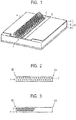
- a semiconductor laser device 1 is bonded to a substrate, which is referred to as a submount 6, in which a metal layer 4 of Au or the like is formed on a ceramics substrate 5 of AlN or the like. Furthermore, bonding wires 2 of Au or the like are connected to an electrode layer of the semiconductor laser device 1 as an electrical connection region used for injecting a current to the semiconductor laser device 1.
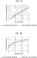
- FIG. 2 illustrates the configuration in which many bonding wires 2 are evenly arranged on the electrode layer of the high power semiconductor laser device 1 as an example of a conventional art (first conventional configuration).
- the diameter of the bonding wire 2 is significantly thin such as around 15 ⁇ m to 50 ⁇ m, it is necessary to connect a significantly large number of bonding wires 2 to the electrode layer of the semiconductor laser device 1 in a high power semiconductor laser device of several watts to 20 watts to which a large current of several amperes to 30 amperes is injected.
- the increased number of bonding wires 2 causes a disadvantage of an increase in cost of a material such as Au, an increase in process tact time, or the like.
- the surface area of the semiconductor laser device 1 is significantly small (for example, 0.3 mm to 0.5 mm in width by 3 mm to 5 mm in length), there is a problem of a limited footprint used for connection of the bonding wires 2.
- Patent Literature 1 for the purpose of reducing the number of bonding wires without deteriorating the performance of a semiconductor laser device in a high power semiconductor laser device.
- Patent Literature 1 Japanese Patent No. 3672272
- Patent Literature 1 discloses that, since the consumption rate of carriers inside the active layer is slow in a region having a low photon density inside the active layer and is fast in a region having a high photon density, when a current supplied (injected) to the semiconductor laser device is even in the longitudinal direction of a resonator, carriers are insufficient in a region having a high photon density inside the active layer, and carriers are excessive in a region having a low photon density. Further, it is disclosed that such insufficient carriers inside the active layer cause the optical output of the semiconductor laser to be saturated. Further, to solve this problem, it is proposed to bond the wires to a position in the longitudinal direction of a resonator corresponding to a local maximum point in the longitudinal direction of the resonator in the photon density distribution inside the active layer.
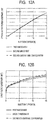
- the inventors have studied a configuration as illustrated in FIG. 3 (second conventional configuration) with reference to Patent Literature 1. That is, in the semiconductor laser device 1 in which the reflectivity of a reflective layer formed on a first facet E1 is lower than the reflectivity of a reflective layer formed on a second facet E2, the first facet E1 part is the local maximum point of the photon density. Furthermore, the bonding wires 2, the number of which is the same as that of the configuration of FIG. 2 , were arranged only on the first facet E1 side so as to be able to flow a current of several amperes or more in the high power semiconductor laser device 1.
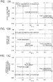
- the drive voltage is undesirably, significantly increased in the second conventional configuration that references Patent Literature 1 while the optical output power is increased as expected. It is considered that this is because the bonding wires 2 generates heat and the electrical resistance increases due to current concentration to the bonding wires 2 bonded only on the first facet E1 side where the consumption rate of carriers is high.
- the WPE is defined as a rate of the operating optical output power of a semiconductor laser device to supplied power (a product of a current and a voltage).
- WPE Wide Plug Efficiency
- the present invention provides a good performance optical semiconductor device, in particular, a high power semiconductor laser device that increases the optical output power while reducing the drive voltage, in particular, realizes an increase in the WPE.
- an optical semiconductor device having: an optical semiconductor device including a semiconductor multilayer structure, an active region interposed between a first facet on a light emitting side and a second facet opposing to the first facet, and a first electrode layer provided on a top of the semiconductor multilayer structure and a second electrode layer provided on a bottom of the semiconductor multilayer structure; and an electrical connection region connected to at least one of the first electrode layer and the second electrode layer of the optical semiconductor device and used for injecting a current to the active region, in which ⁇ > ⁇ and ⁇ > 0 are satisfied, where in a contact area between the electrical connection region and the optical semiconductor device, the contact area included in a half region on the first facet side in a top area of the optical semiconductor device is denoted as ⁇ , and the contact area included in a half region on the second facet side is denoted as ⁇ .
- the optical semiconductor device described above in which a part of the electrical connection region connected to the half region on the second facet side in a top area of the optical semiconductor device is located near the second facet.
- the optical semiconductor device described above in which a part of the electrical connection region connected to the half region on the second facet side in a top area of the optical semiconductor device is located in a quarter region from the second facet side.
- the optical semiconductor device described above in which the electrical connection region is arranged and connected such that a current density distribution in a direction connecting the first facet and the second facet inside the active region is close to a photon density distribution in the same direction inside the active region.
- the optical semiconductor device described above in which the optical semiconductor device is a semiconductor laser device in which the optical output power from the first facet is greater than or equal to 100 mW.
- the optical semiconductor device described above in which the optical output power from the first facet is greater than or equal to 1 W, and the optical semiconductor device is a semiconductor laser device that oscillates the multimode laser.
- the optical semiconductor device described above in which the optical semiconductor device is a semiconductor optical amplifier device that is inputted with a laser from the second facet and outputs, from the first facet, the optical output power is greater than or equal to 10 mW.
- the semiconductor laser device 1 is an edge emission-type semiconductor laser device that oscillates the multimode laser.
- oscillates the multimode laser as used herein means that a semiconductor laser device has a wide waveguide that allows a plurality of waveguide modes.
- FIG. 5 is a schematic perspective view of the semiconductor laser device 1 according to the embodiment of the present invention.
- the semiconductor laser device 1 has a semiconductor multilayer structure 8, and an active region 11 interposed between a first facet E1 on a light emitting side and a second facet E2 opposing to the first facet E1.
- the semiconductor laser device 1 guides a laser within the active region 11 and emits a laser through the low reflective layer 9 from the first facet E1.
- the semiconductor laser length L of the semiconductor laser device 1 that is determined by the distance between the first facet E1 and the second facet E2 is, for example, 1 mm to 6 mm, more preferably, around 3 mm to 5 mm.
- FIG. 6 is an example of a sectional view of the semiconductor laser device 1 illustrated in FIG. 5 .
- the semiconductor laser device 1 has a first electrode layer 23 formed on the top face, a second electrode layer 13 formed on the bottom face, a substrate 14 made of n-type GaAs, the semiconductor multilayer structure 8 formed on the substrate 14, and a passivation layer 22.
- the semiconductor multilayer structure 8 has an n-type buffer layer 15, an n-type clad layer 16, an n-type waveguide layer 17, an active layer 18, a p-type waveguide layer 19, a p-type clad layer 20, and a p-type contact layer 21 that are formed on the substrate 14 in this order.
- the n-type buffer layer 15 is made of GaAs and is a buffer layer to grow a multilayer structure of a high quality epitaxial layer on the substrate 14.
- the n-type clad layer 16 and the n-type waveguide layer 17 are made of AlGaAs whose refractive index and thickness are set so as to realize a desired optical confinement factor in a stacking direction. Note that the Al composition of the n-type waveguide layer 17 is more than or equal to 20% and less than 40%, for example. Further, the reflection index of the n-type clad layer 16 is smaller than the same of the n-type waveguide layer 17.
- the thickness of the n-type waveguide layer 17 is preferably greater than or equal to 50 nm, for example, equal to around 1000 nm.
- the thickness of the n-type clad layer 16 is preferably around 1 ⁇ m to 3 ⁇ m.
- these n-type semiconductor layers include silicon (Si), for example, as an n-type dopant.
- the active layer 18 has a bottom barrier layer 18a, a quantum well layer 18b, and a top barrier layer 18c and has single quantum well (SQW) structure.
- the bottom barrier layer 18a and the top barrier layer 18c have a function of a barrier that confines carriers in the quantum well layer 18b and are made of high purity AlGaAs without intentional dope.
- the quantum well layer 18b is made of high purity InGaAs without intentional dope.
- the In composition and the thickness of the quantum well layer 18b and the compositions of the bottom barrier layer 18a and the top barrier layer 18c are set in accordance with a desired light emission center wavelength (for example, 900 nm to 1080 nm) .
- the structure of the active layer 18 may be multiple quantum well (MQW) structure in which a desired number of stacked structures of the quantum well layer 18b and barrier layers formed above and below the quantum well layer 18b are repeatedly arranged or may be single quantum well structure.
- MQW multiple quantum well
- a donor and an accepter may be intentionally added to the quantum well layer 18b, the bottom barrier layer 18a, and the top barrier layer 18c.
- the p-type waveguide layer 19 and the p-type clad layer 20 are paired with the n-type clad layer 16 and the n-type waveguide layer 17 described above, respectively, and are made of AlGaAs whose refractive index and thickness are set so as to realize a desired optical confinement factor in the stacking direction.
- the Al composition of the p-type waveguide layer 19 is greater than or equal to 20% and less than 40%, for example.
- the refractive index of the p-type clad layer 20 is smaller than that of the p-type waveguide layer 19.
- the Al composition of the p-type clad layer 20 is set slightly larger than the Al composition of the n-type clad layer 16 in order to reduce waveguide loss by adjusting a field of light in a layer to the direction of the n-type clad layer 16.
- the Al composition of the p-type waveguide layer 19 is then set smaller than that of the p-type clad layer 20.
- the thickness of the p-type waveguide layer 19 is preferably greater than or equal to 50 nm, for example, equal to around 1000 nm.
- the thickness of the p-type clad layer 20 is preferably around 1 ⁇ m to 3 ⁇ m.
- these p-type semiconductor layers include carbon (C) as a p-type dopant.
- the C concentration of the p-type waveguide layer 19 is set to, for example, 0.1 to 1.0 ⁇ 10 17 cm -3 , preferably, around 0.5 to 1.0 ⁇ 10 17 cm -3 .
- the C concentration of the p-type clad layer 20 is set to be greater than or equal to 1.0 ⁇ 10 17 cm -3 , for example.
- the p-type contact layer 21 is made of GaAs doped with Zn or C at a high concentration.
- the first electrode layer 23 is formed on the top face of the p-type contact layer 21.
- the first electrode layer 23 is made of, for example, a metal layer of Ti/Pt/Au, an alloy layer whose primary composition is Au or Zn, or the like and the thickness thereof is less than or equal to 2 ⁇ m, more preferably, 0.5 ⁇ m to 0.1 ⁇ m, for example.
- Au plating of a thickness of 10 to 3 ⁇ m, for example, may be formed on the top face of the first electrode layer 23 in order to obtain good electrical connection to the first electrode layer 23.
- the second electrode layer 13 is formed on the bottom face of the substrate 14 made of an n-type GaAs.
- the second electrode layer 13 is made of, for example, an alloy layer that is composed of Au, Ge, and Ni, and the thickness thereof is less than or equal to 2 ⁇ m, more preferably, 0.5 to 0.1 ⁇ m, for example.
- a ridge structure for confining a light in the horizontal direction in FIG. 6 is formed in a region directly under an opening region 22a of the semiconductor multilayer structure 8.
- a waveguide width 12 determined by the width of the bottom of the ridge structure is, for example, greater than or equal to 80 ⁇ m and less than or equal to 500 ⁇ m.
- the passivation layer 22 is an insulating film made of SiNx, for example, and has the opening region 22a.
- current constriction to the active region 11 is achieved by restricting the contact area between the first electrode layer 23 and the semiconductor multilayer structure 8 by using the passivation layer 22.
- the semiconductor laser device 1 formed as described above is bonded on a submount 6, in addition, the bonding wires 2 of Au or the like are connected thereto as the electrical connection region used for injecting a current to the semiconductor laser device 1, and thereby a semiconductor laser device is assembled.
- the submount 6 one in which a metal film 4 of Au or the like is formed on a substrate of a CuW alloy or the like is used, or one in which a metal film 4 of Au or the like is formed on a ceramics substrate of AlN or the like is used, for example. Further, for example, solder 7 of an AuSn alloy or the like is used to bond the semiconductor laser device 1 to the submount 6.
- junction-up bonding a bonding wire or the like of Au or the like is connected to a first electrode layer of a semiconductor laser device as an electrical connection region used for injecting a current to an active region, for example.
- the diameter of the bonding wire is 15 to 50 ⁇ m, for example.
- the other method is a method for bonding a semiconductor laser device to a submount via a first electrode layer and is called junction-down bonding.
- a bonding wire or the like of Au or the like is connected to a second electrode layer of a semiconductor laser device as an electrical connection region used for injecting a current to an active region, for example.
- the junction-down bonding is often used.
- the bonding wires 2 are connected to the second electrode layer 13 in a configuration illustrated in FIG. 8 .
- the contact area included in a half region on the first facet E1 side of the top area of the semiconductor laser device 1 is denoted as ⁇
- the contact area included in a half region on the second facet E2 side of the top area is denoted as ⁇ .
- the bonding wires 2 are connected so as to satisfy ⁇ > ⁇ .
- a contact area 24 for every single bonding wire 2 may be defined as the area by which the end of the bonding wire 2 contacts onto the second electrode layer 13, as illustrated in FIG. 9 , for example.
- a value obtained by multiplying the contact area 24 per a single bonding wire 2 by the number of bonding wires 2 located in the half region on the first facet E1 side of the top area of the semiconductor laser device 1 is ⁇
- a value obtained by multiplying the contact area 24 per a single bonding wire 2 by the number of bonding wires 2 located in the half region on the second facet E2 side is ⁇ .
- At least one (in this example, two) bonding wire 2 is connected onto the second facet E2 side of the top area of the semiconductor laser device 1, and thus ⁇ > 0.
- the bonding wires 2 are arranged on and connected to the second electrode layer 13 in a configuration illustrated in FIG. 10 . That is, ⁇ > ⁇ is satisfied, where in the contact area between the electrical connection region described above and the second electrode layer 13, the contact area included in a half region on the first facet E1 side of the top area of the semiconductor laser device 1 is denoted as ⁇ and the contact area included in a half region on the second facet E2 side of the top area is denoted as ⁇ , and at least one bonding wire 2 is connected to the second facet E2 side of the top area of the semiconductor laser device 1 and thus ⁇ > 0. Furthermore, the bonding wires 2 are arranged such that the current density distribution in a direction connecting the first facet E1 and the second facet E2 inside the active region 11 of the semiconductor laser device 1 is close to the photon density distribution in the same direction.
- optical intensity distribution inside the active region 11 of the semiconductor laser device 1 was calculated by using equations below.
- the value A denotes a proportional coefficient
- the value Rf denotes the reflectivity of the low reflective layer 9 formed on the first facet E1
- the value Rb denotes the reflectivity of the high reflective layer 10 formed on the second facet E2
- the value L is the semiconductor laser length defined by the distance between the first facet E1 and the second facet E2.
- the bonding wires 2 are arranged on and connected to the second electrode layer 13 such that the bonding wires 2 are arranged most densely on the first facet E1 side where the optical intensity is the largest and, in a portion closer to the second facet E2 side, the density of the bonding wires 2 is reduced in proportion to a reduction in the optical intensity.
- FIG. 12A and FIG. 12B illustrate the results.
- the drive voltage was reduced in the arrangement of the bonding wires 2 of the first embodiment in which the relationship of ⁇ > ⁇ and ⁇ > 0 are satisfied, where in the contact area between the electrical connection region and the second electrode layer 13, the contact area included in a half region on the first facet E1 side of the top area of the semiconductor laser device 1 is denoted as ⁇ and the contact area included in a half region on the second facet E2 side is denoted as ⁇ .
- the drive voltage is further reduced in the configuration of the second embodiment in which the bonding wires 2 are arranged such that the relationship of ⁇ > ⁇ and ⁇ > 0 are satisfied, where in the contact area between the electrical connection region and the second electrode layer 13, the contact area included in a half region on the first facet E1 side of the top area of the semiconductor laser device 1 is denoted as ⁇ and the contact area included in a half region on the second facet E2 side is denoted as ⁇ , and the current density distribution in the direction connecting the first facet E1 and the second facet E2 inside the active region 11 is close to the photon density distribution in the same direction.
- the optical output power of the first embodiment and the second embodiment was not substantially reduced compared to the optical output power of the second conventional configuration.
- FIG. 13A, FIG. 13B, and FIG. 13C illustrate results of comparison in terms of the optical output power, the drive voltage, and the electrical-optical conversion efficiency between four configurations of the first conventional configuration, the second conventional configuration, the first embodiment, and the second embodiment.
- the first conventional configuration in which many bonding wires are evenly arranged has the lowest WPE
- the second conventional configuration in which many bonding wires are arranged only on the first facet side has large optical output power but has a large drive voltage resulting in a poor WPE.
- the drive voltage is significantly reduced, and thus the WPE is high.
- the WPE was the highest in the second embodiment in which the bonding wires 2 are arranged such that the relationship of ⁇ > ⁇ and ⁇ > 0 are satisfied, where in the contact area between the electrical connection region and the second electrode layer 13, the contact area included in a half region on the first facet E1 side of the top area of the semiconductor laser device 1 is denoted as ⁇ and the contact area included in a half region on the second facet E2 side of the top area is denoted as ⁇ , and the current density distribution in the direction connecting the first facet E1 and the second facet E2 inside the active region is close to the photon density distribution in the same direction, which indicates the most preferable arrangement of the bonding wires.
- the electrical resistance of an electrode layer to which the electrical connection region such as the bonding wires is connected is required to be sufficiently larger than the electrical connection region such as the bonding wires.
- the thickness of the first electrode layer 23 formed of a metal layer of Ti/Pt/Au, an alloy layer whose primary component is Au or Zn, or the like, for example, is 2 ⁇ m or less, more preferably, 0.5 to 0.1 ⁇ m, for example.
- the thickness of the second electrode layer 13 formed of an alloy layer composed of Au, Ge, and Ni or the like, for example, is 2 ⁇ m or less, more preferably, 0.5 to 0.1 ⁇ m, for example.
- the present embodiment is an application example of the first embodiment.
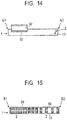
- a bonding ribbon 32 that is an Au foil or the like shaped in a ribbon is connected to the second electrode layer 13 on the first facet E1 side in a configuration illustrated in FIG. 14 instead of many bonding wires 2 being connected in the first embodiment.
- at least one (in this example, two) bonding wire 2 is connected on the second facet E2 side.
- the relationship of ⁇ > ⁇ is satisfied, where in the contact area between the electrical connection region described above and the second electrode layer 13, the contact area included in a half region on the first facet E1 side of the top area of the semiconductor laser device 1 is denoted as ⁇ and the contact area included in a half region on the second facet E2 side of the top area is denoted as ⁇ .
- the contact area between the second electrode layer 13 and the bonding ribbon 32 as the electrical connection region is the area of the connection region 33 of the bonding ribbon 32.
- the area included in the half region on the first facet E1 side of the top area of the semiconductor laser device 1 corresponds to ⁇ .
- the present embodiment is an application example of the second embodiment. That is, pads 56 are formed on the top of the second electrode layer 13 of the semiconductor laser device 1, and furthermore the bonding wires 2 are connected on the pads 56 in a configuration illustrated in FIG. 15 .
- Each of the pads 56 is formed of Au plating or the like having a small electrical resistance, and the thickness thereof is 3 ⁇ m to 10 ⁇ m, for example. It can be considered that the pad 56 and the bonding wire 2 connected on the pad 56 have the same electric potential. Therefore, in the present embodiment, the pads 56 correspond to the electrical connection region connected to the second electrode layer 13 of the semiconductor laser device 1.
- the relationship of ⁇ > ⁇ is satisfied, where in the contact area between the electrical connection region described above and the second electrode layer 13, the contact area included in a half region on the first facet E1 side of the top area of the semiconductor laser device 1 is denoted as ⁇ and the contact area included in a half region on the second facet E2 side of the top area is denoted as ⁇ .
- the contact area between the electrical connection region and the second electrode layer 13 corresponds to the areas of the pads 56.
- the sum of the areas included in the half region on the first facet E1 side of the top area of the semiconductor laser device 1 corresponds to ⁇
- the sum of the areas included in the half region on the second facet E2 side corresponds to ⁇
- at least one pad 56 is located on the second facet E2 side of the top area of the semiconductor laser device 1, and thus ⁇ > 0.
- the pads 56 are formed on the second electrode layer 13 of the semiconductor laser device 1 such that the current density distribution in the direction connecting the first facet E1 and the second facet E2 inside the active region 11 of the semiconductor laser device 1 is close to the photon density distribution in the same direction. Therefore, the present embodiment is one example of the most preferable arrangement of the electrical connection region, and a good performance semiconductor laser device in which an increase in WPE is realized can be obtained as with the second embodiment.
- the present embodiment is an application example of the second embodiment. That is, a substantially triangular pad 56 is formed on the top of the second electrode layer 13 of the semiconductor laser device 1 such that the first facet E1 side of the semiconductor laser device 1 corresponds to the base and the second facet E2 side corresponds to the vertex in a configuration as illustrated in FIG. 16 . Furthermore, the bonding wires 2 are connected onto the pad 56.
- the pad 56 is formed of an Au plating or the like having a small electrical resistance, and the thickness thereof is 3 ⁇ m to 10 ⁇ m, for example. It can be considered that the pad 56 and the bonding wire 2 connected on the pad 56 have the same electric potential. Therefore, in the present embodiment, the pad 56 corresponds to the electrical connection region connected to the second electrode layer 13 of the semiconductor laser device 1 as with the fourth embodiment.
- the relationship of ⁇ > ⁇ is satisfied, where in the contact area between the electrical connection region described above and the second electrode layer 13, the contact area included in a half region on the first facet E1 side of the top area of the semiconductor laser device 1 is denoted as ⁇ and the contact area included in a half region on the second facet E2 side of the top area is denoted as ⁇ .
- the contact area between the electrical connection region and the second electrode layer 13 corresponds to the area of the pad 56.
- the integrated pad 56 is arranged, in the area of the pad 56, the area of a portion included in the half region on the first facet E1 side of the top area of the semiconductor laser device 1 corresponds to ⁇ , and similarly, the area of a portion included in the half region on the second facet E2 side corresponds to ⁇ . Further, the pad 56 has a substantially triangular shape such that the second facet E2 side of the top area of the semiconductor laser device 1 corresponds to the vertex, and thus ⁇ > 0.
- the pad 56 is formed on the second electrode layer 13 of the semiconductor laser device 1 such that the current density distribution in the direction connecting the first facet E1 and the second facet E2 inside the active region 11 of the semiconductor laser device 1 is close to the photon density distribution in the same direction. That is, the width of the pad 56 (the width orthogonal to the direction connecting the first facet E1 and the second facet E2) is the largest on the first facet E1 side of the semiconductor laser device 1 and decreases as approaching the second facet E2 side in accordance with the optical intensity distribution illustrated in FIG. 11 . In such a way, by designing the shape of the pad 56 as the electrical connection region connected to the second electrode layer 13 of the semiconductor laser device 1, it is possible to supply carriers efficiently inside the active region 11. Therefore, the present embodiment is one example of the most preferable configuration of the electrical connection region, and a good performance semiconductor laser device in which an increase in WPE is realized can be obtained as with the second embodiment.
- the present embodiment is a modified example of the second embodiment. That is, as the electrical connection region, the bonding wires 2 are arranged on and connected to the second electrode layer 13 of the semiconductor laser device 1 not in the form of two lines but in the form of a single line in a configuration illustrated in FIG. 17 .
- the bonding wires are not necessarily required to be formed in two lines. It is not preferable to connect more bonding wires than is needed to the electrode layer of the semiconductor laser device, because such connection causes disadvantages of an increase in cost of the material such as Au, an increase in process tact time, or the like.
- the relationship of ⁇ > ⁇ is satisfied, where in the contact area between the electrical connection region described above and the second electrode layer 13, the contact area included in a half region on the first facet E1 side of the top area of the semiconductor laser device 1 is denoted as ⁇ and the contact area included in a half region on the second facet E2 side of the top area is denoted as ⁇ , and at least one bonding wire 2 is connected on the second facet E2 side of the top area of the semiconductor laser device 1 and thus ⁇ > 0.
- the bonding wires 2 are arranged in a form of a single line such that the current density distribution in the direction connecting the first facet E1 and the second facet E2 inside the active region 11 of the semiconductor laser device 1 is close to the photon density distribution in the same direction. Therefore, in a semiconductor laser device of the optical output power around 10 mW to 2 W, for example, the present embodiment is one example of the most preferable arrangement of the electrical connection region, and a good performance semiconductor laser device in which an increase in WPE is realized can be obtained.
- the semiconductor laser device may be bonded to the submount by junction-down bonding and the electrical connection region is connected to or formed on the second electrode layer.
- the semiconductor laser device may be bonded to the submount by junction-up bonding, and the electrical connection region may be connected to or formed on the first electrode layer.
- the type of the optical semiconductor device is not particularly limited.
- the optical semiconductor device may be a semiconductor optical amplifier which is input with a laser from the second facet and outputs a laser whose optical output power is 10 mW or higher from the first facet.
- the optical semiconductor device may be a semiconductor integrated circuit device in which a semiconductor laser device and an optical semiconductor amplifier are integrated.
Landscapes
- Physics & Mathematics (AREA)
- Condensed Matter Physics & Semiconductors (AREA)
- General Physics & Mathematics (AREA)
- Electromagnetism (AREA)
- Optics & Photonics (AREA)
- Geometry (AREA)
- Semiconductor Lasers (AREA)
Abstract
Description
- The present invention relates to an optical semiconductor device, in particular, a semiconductor laser device in which the optical output power of the laser is 100 mW or higher, furthermore, a high power semiconductor laser device in which the optical output power of the laser is several watts or higher.
- The semiconductor laser device is utilized as a laser used for optical communication, an industrial laser used for processing or the like, or the like. The laser used for optical communication is required to propagate a light in an optical fiber over a long distance (for example, several hundred kilometers), and a single mode laser is used in general in order to suppress deterioration of signal quality. On the other hand, since an industrial laser requires higher power than an optical communication laser but does not require long distance propagation, a multimode laser dedicated to high power is used for the industrial laser. In a multimode laser, high power is achieved by increasing the width of a laser waveguide to allow a plurality of modes (that is, multimode) inside the waveguide. Here, high power means optical output power of around several watts to 20 watts (both at a room temperature and in CW operation), for example, as the optical output power of a laser.
- In a general semiconductor laser has a semiconductor multilayer structure formed on a substrate, an active region interposed between a first facet on a light emitting side and a second facet opposing to the first facet, a first electrode layer provided on the top of the semiconductor multilayer structure, and a second electrode layer provided on the bottom of the semiconductor multilayer structure.
- In a high power semiconductor laser device, as illustrated in
FIG. 1 , asemiconductor laser device 1 is bonded to a substrate, which is referred to as asubmount 6, in which ametal layer 4 of Au or the like is formed on aceramics substrate 5 of AlN or the like. Furthermore,bonding wires 2 of Au or the like are connected to an electrode layer of thesemiconductor laser device 1 as an electrical connection region used for injecting a current to thesemiconductor laser device 1.FIG. 2 illustrates the configuration in whichmany bonding wires 2 are evenly arranged on the electrode layer of the high powersemiconductor laser device 1 as an example of a conventional art (first conventional configuration). In general, since the diameter of thebonding wire 2 is significantly thin such as around 15 µm to 50 µm, it is necessary to connect a significantly large number ofbonding wires 2 to the electrode layer of thesemiconductor laser device 1 in a high power semiconductor laser device of several watts to 20 watts to which a large current of several amperes to 30 amperes is injected. However, the increased number ofbonding wires 2 causes a disadvantage of an increase in cost of a material such as Au, an increase in process tact time, or the like. Furthermore, since the surface area of thesemiconductor laser device 1 is significantly small (for example, 0.3 mm to 0.5 mm in width by 3 mm to 5 mm in length), there is a problem of a limited footprint used for connection of thebonding wires 2. - Accordingly, the inventors have referenced
Patent Literature 1 for the purpose of reducing the number of bonding wires without deteriorating the performance of a semiconductor laser device in a high power semiconductor laser device. - Patent Literature 1: Japanese Patent No.
3672272 -
Patent Literature 1 discloses that, since the consumption rate of carriers inside the active layer is slow in a region having a low photon density inside the active layer and is fast in a region having a high photon density, when a current supplied (injected) to the semiconductor laser device is even in the longitudinal direction of a resonator, carriers are insufficient in a region having a high photon density inside the active layer, and carriers are excessive in a region having a low photon density. Further, it is disclosed that such insufficient carriers inside the active layer cause the optical output of the semiconductor laser to be saturated. Further, to solve this problem, it is proposed to bond the wires to a position in the longitudinal direction of a resonator corresponding to a local maximum point in the longitudinal direction of the resonator in the photon density distribution inside the active layer. - The inventors have studied a configuration as illustrated in
FIG. 3 (second conventional configuration) with reference toPatent Literature 1. That is, in thesemiconductor laser device 1 in which the reflectivity of a reflective layer formed on a first facet E1 is lower than the reflectivity of a reflective layer formed on a second facet E2, the first facet E1 part is the local maximum point of the photon density. Furthermore, thebonding wires 2, the number of which is the same as that of the configuration ofFIG. 2 , were arranged only on the first facet E1 side so as to be able to flow a current of several amperes or more in the high powersemiconductor laser device 1. - As illustrated in
FIG. 4A and FIG. 4B , however, in comparison in terms of the optical output power and the drive voltage between the first conventional configuration in whichmany bonding wires 2 are evenly arranged (the configuration inFIG. 2 ) and the second conventional configuration in which thebonding wires 2, the number of which is the same as that in the first conventional configuration, are arranged only on the first facet E1 side (the configuration inFIG. 3 ), the drive voltage is undesirably, significantly increased in the second conventional configuration that referencesPatent Literature 1 while the optical output power is increased as expected. It is considered that this is because thebonding wires 2 generates heat and the electrical resistance increases due to current concentration to thebonding wires 2 bonded only on the first facet E1 side where the consumption rate of carriers is high. - In industrial lasers, a high electrical-optical conversion efficiency (Wall Plug Efficiency (WPE)) is demanded. The WPE is defined as a rate of the operating optical output power of a semiconductor laser device to supplied power (a product of a current and a voltage). Thus, an increase in the drive voltage results in a reduction in the WPE, which is not preferable in terms of the performance of a semiconductor laser.
- The present invention provides a good performance optical semiconductor device, in particular, a high power semiconductor laser device that increases the optical output power while reducing the drive voltage, in particular, realizes an increase in the WPE.
- According to one aspect of the present invention, provided is an optical semiconductor device having: an optical semiconductor device including a semiconductor multilayer structure, an active region interposed between a first facet on a light emitting side and a second facet opposing to the first facet, and a first electrode layer provided on a top of the semiconductor multilayer structure and a second electrode layer provided on a bottom of the semiconductor multilayer structure; and an electrical connection region connected to at least one of the first electrode layer and the second electrode layer of the optical semiconductor device and used for injecting a current to the active region, in which α > β and β > 0 are satisfied, where in a contact area between the electrical connection region and the optical semiconductor device, the contact area included in a half region on the first facet side in a top area of the optical semiconductor device is denoted as α, and the contact area included in a half region on the second facet side is denoted as β.
- According to another aspect of the present invention, provided is the optical semiconductor device described above in which a part of the electrical connection region connected to the half region on the second facet side in a top area of the optical semiconductor device is located near the second facet.
- According to another aspect of the present invention, provided is the optical semiconductor device described above in which a part of the electrical connection region connected to the half region on the second facet side in a top area of the optical semiconductor device is located in a quarter region from the second facet side.
- According to another aspect of the present invention, provided is the optical semiconductor device described above in which the electrical connection region is arranged and connected such that a current density distribution in a direction connecting the first facet and the second facet inside the active region is close to a photon density distribution in the same direction inside the active region.
- According to another aspect of the present invention, provided is the optical semiconductor device described above in which the optical semiconductor device is a semiconductor laser device in which the optical output power from the first facet is greater than or equal to 100 mW.
- According to another aspect of the present invention, provided is the optical semiconductor device described above in which the optical output power from the first facet is greater than or equal to 1 W, and the optical semiconductor device is a semiconductor laser device that oscillates the multimode laser.
- According to another aspect of the present invention, provided is the optical semiconductor device described above in which the optical semiconductor device is a semiconductor optical amplifier device that is inputted with a laser from the second facet and outputs, from the first facet, the optical output power is greater than or equal to 10 mW.
-
- [
FIG. 1] FIG. 1 is a perspective view of an example of a semiconductor laser device according to a conventional configuration. - [
FIG. 2] FIG. 2 is a top view illustrating the arrangement of an electrical connection region in a first conventional configuration. - [
FIG. 3] FIG. 3 is a top view illustrating the arrangement of an electrical connection region in a second conventional configuration. - [
FIG. 4A] FIG. 4A is a graph illustrating a result of comparison in terms of the optical output power and the drive voltage between the first conventional configuration and the second conventional configuration. - [
FIG. 4B] FIG. 4B is a graph illustrating a result comparison in terms of the optical output power and the drive voltage between the first conventional configuration and the second conventional configuration. - [
FIG. 5] FIG. 5 is a schematic perspective view of a semiconductor laser device according to the present invention. - [
FIG. 6] FIG. 6 is a schematic sectional view of the semiconductor laser device illustrated inFIG. 5 . - [
FIG. 7] FIG. 7 is a perspective view of an example of a semiconductor laser device according to the present invention. - [
FIG. 8] FIG. 8 is a top view illustrating the arrangement of an electrical connection region in a first embodiment of the present invention. - [
FIG. 9] FIG. 9 is a diagram illustrating the contact area between a bonding wire and a first electrode layer or a second electrode layer. - [
FIG. 10] FIG. 10 is a top view illustrating the arrangement of an electrical connection region in a second embodiment of the present invention. - [
FIG. 11] FIG. 11 is a graph illustrating an optical intensity distribution inside an active region. - [
FIG. 12A] FIG. 12A is a graph illustrating a result of comparison and examination in terms of the optical output power and the drive voltage between the embodiments of the present invention and the conventional configuration. - [
FIG. 12B] FIG. 12B is a graph illustrating a result of comparison and examination in terms of the optical output power and the drive voltage between the embodiments of the present invention and the conventional configuration. - [
FIG. 13A] FIG. 13A is a graph illustrating an advantage of improvement in the electrical-optical conversion efficiency in the embodiments of the present invention in comparison between the embodiments of the present invention and the conventional configurations. - [
FIG. 13B] FIG. 13B is a graph illustrating an advantage of improvement in the electrical-optical conversion efficiency in the embodiments of the present invention in comparison between the embodiments of the present invention and the conventional configurations. - [
FIG. 13C] FIG. 13C is a graph illustrating an advantage of improvement in the electrical-optical conversion efficiency in the embodiments of the present invention in comparison between the embodiments of the present invention and the conventional configurations. - [
FIG. 14] FIG. 14 is a top view illustrating a modified example of the arrangement of an electrical connection region according to the present invention. - [
FIG. 15] FIG. 15 is a top view illustrating a modified example of the arrangement of an electrical connection region according to the present invention. - [
FIG. 16] FIG. 16 is a top view illustrating a modified example of the arrangement of an electrical connection region according to the present invention. - [
FIG. 17] FIG. 17 is a top view illustrating a modified example of the arrangement of an electrical connection region according to the present invention. - The embodiments of an optical semiconductor device according to the present invention will be described below with reference to the drawings. Note that the present invention is not limited to these embodiments. Further, in illustration of the drawings, the same or corresponding devices are labeled with the same reference if necessary. Further, it is noted that each drawing is schematic illustration, and the relationship between dimensions of respective devices, the ratio of respective devices, or the like may be different from the actual implementation. Portions having different dimensional relationships or ratios may also be included throughout the drawings.
- First, a
semiconductor laser device 1 as an example of an optical semiconductor device according to an embodiment of the present invention will be described. Thesemiconductor laser device 1 according to the present embodiment is an edge emission-type semiconductor laser device that oscillates the multimode laser. Note that "oscillates the multimode laser" as used herein means that a semiconductor laser device has a wide waveguide that allows a plurality of waveguide modes. -
FIG. 5 is a schematic perspective view of thesemiconductor laser device 1 according to the embodiment of the present invention. As illustrated inFIG. 5 , thesemiconductor laser device 1 has asemiconductor multilayer structure 8, and anactive region 11 interposed between a first facet E1 on a light emitting side and a second facet E2 opposing to the first facet E1. A lowreflective layer 9 having reflectivity that is lower than or equal to 10%, for example, is formed on the first facet E1 that is the light emitting side of thesemiconductor multilayer structure 8, and a highreflective layer 10 having reflectivity that is higher than or equal to 90%, for example, is formed on the second facet E2 opposing to the first facet E1. Thesemiconductor laser device 1 guides a laser within theactive region 11 and emits a laser through the lowreflective layer 9 from the first facet E1. - The semiconductor laser length L of the
semiconductor laser device 1 that is determined by the distance between the first facet E1 and the second facet E2 is, for example, 1 mm to 6 mm, more preferably, around 3 mm to 5 mm. -
FIG. 6 is an example of a sectional view of thesemiconductor laser device 1 illustrated inFIG. 5 . As illustrated inFIG. 6 , thesemiconductor laser device 1 has afirst electrode layer 23 formed on the top face, asecond electrode layer 13 formed on the bottom face, asubstrate 14 made of n-type GaAs, thesemiconductor multilayer structure 8 formed on thesubstrate 14, and apassivation layer 22. - The
semiconductor multilayer structure 8 has an n-type buffer layer 15, an n-type clad layer 16, an n-type waveguide layer 17, anactive layer 18, a p-type waveguide layer 19, a p-type cladlayer 20, and a p-type contact layer 21 that are formed on thesubstrate 14 in this order. - The n-
type buffer layer 15 is made of GaAs and is a buffer layer to grow a multilayer structure of a high quality epitaxial layer on thesubstrate 14. The n-type clad layer 16 and the n-type waveguide layer 17 are made of AlGaAs whose refractive index and thickness are set so as to realize a desired optical confinement factor in a stacking direction. Note that the Al composition of the n-type waveguide layer 17 is more than or equal to 20% and less than 40%, for example. Further, the reflection index of the n-type clad layer 16 is smaller than the same of the n-type waveguide layer 17. Further, the thickness of the n-type waveguide layer 17 is preferably greater than or equal to 50 nm, for example, equal to around 1000 nm. The thickness of the n-type clad layer 16 is preferably around 1 µm to 3 µm. Further, these n-type semiconductor layers include silicon (Si), for example, as an n-type dopant. - The
active layer 18 has abottom barrier layer 18a, aquantum well layer 18b, and atop barrier layer 18c and has single quantum well (SQW) structure. Thebottom barrier layer 18a and thetop barrier layer 18c have a function of a barrier that confines carriers in thequantum well layer 18b and are made of high purity AlGaAs without intentional dope. Thequantum well layer 18b is made of high purity InGaAs without intentional dope. The In composition and the thickness of thequantum well layer 18b and the compositions of thebottom barrier layer 18a and thetop barrier layer 18c are set in accordance with a desired light emission center wavelength (for example, 900 nm to 1080 nm) . Note that the structure of theactive layer 18 may be multiple quantum well (MQW) structure in which a desired number of stacked structures of thequantum well layer 18b and barrier layers formed above and below thequantum well layer 18b are repeatedly arranged or may be single quantum well structure. Further, while the configuration without intentional dope on a high purity layer is illustrated above, a donor and an accepter may be intentionally added to thequantum well layer 18b, thebottom barrier layer 18a, and thetop barrier layer 18c. - The p-
type waveguide layer 19 and the p-type cladlayer 20 are paired with the n-type clad layer 16 and the n-type waveguide layer 17 described above, respectively, and are made of AlGaAs whose refractive index and thickness are set so as to realize a desired optical confinement factor in the stacking direction. Note that the Al composition of the p-type waveguide layer 19 is greater than or equal to 20% and less than 40%, for example. The refractive index of the p-type cladlayer 20 is smaller than that of the p-type waveguide layer 19. The Al composition of the p-type cladlayer 20 is set slightly larger than the Al composition of the n-type clad layer 16 in order to reduce waveguide loss by adjusting a field of light in a layer to the direction of the n-type clad layer 16. The Al composition of the p-type waveguide layer 19 is then set smaller than that of the p-type cladlayer 20. Further, the thickness of the p-type waveguide layer 19 is preferably greater than or equal to 50 nm, for example, equal to around 1000 nm. The thickness of the p-type cladlayer 20 is preferably around 1 µm to 3 µm. Further, these p-type semiconductor layers include carbon (C) as a p-type dopant. The C concentration of the p-type waveguide layer 19 is set to, for example, 0.1 to 1.0 × 1017 cm-3, preferably, around 0.5 to 1.0 × 1017 cm-3. The C concentration of the p-type cladlayer 20 is set to be greater than or equal to 1.0 × 1017 cm-3, for example. Further, the p-type contact layer 21 is made of GaAs doped with Zn or C at a high concentration. - The
first electrode layer 23 is formed on the top face of the p-type contact layer 21. Thefirst electrode layer 23 is made of, for example, a metal layer of Ti/Pt/Au, an alloy layer whose primary composition is Au or Zn, or the like and the thickness thereof is less than or equal to 2 µm, more preferably, 0.5 µm to 0.1 µm, for example. Au plating of a thickness of 10 to 3 µm, for example, may be formed on the top face of thefirst electrode layer 23 in order to obtain good electrical connection to thefirst electrode layer 23. - The
second electrode layer 13 is formed on the bottom face of thesubstrate 14 made of an n-type GaAs. Thesecond electrode layer 13 is made of, for example, an alloy layer that is composed of Au, Ge, and Ni, and the thickness thereof is less than or equal to 2 µm, more preferably, 0.5 to 0.1 µm, for example. - As illustrated in
FIG. 6 , a ridge structure for confining a light in the horizontal direction inFIG. 6 is formed in a region directly under anopening region 22a of thesemiconductor multilayer structure 8. Awaveguide width 12 determined by the width of the bottom of the ridge structure is, for example, greater than or equal to 80 µm and less than or equal to 500 µm. - The
passivation layer 22 is an insulating film made of SiNx, for example, and has theopening region 22a. In thesemiconductor laser device 1, current constriction to theactive region 11 is achieved by restricting the contact area between thefirst electrode layer 23 and thesemiconductor multilayer structure 8 by using thepassivation layer 22. - As illustrated in
FIG. 7 , thesemiconductor laser device 1 formed as described above is bonded on asubmount 6, in addition, thebonding wires 2 of Au or the like are connected thereto as the electrical connection region used for injecting a current to thesemiconductor laser device 1, and thereby a semiconductor laser device is assembled. - As the
submount 6, one in which ametal film 4 of Au or the like is formed on a substrate of a CuW alloy or the like is used, or one in which ametal film 4 of Au or the like is formed on a ceramics substrate of AlN or the like is used, for example. Further, for example,solder 7 of an AuSn alloy or the like is used to bond thesemiconductor laser device 1 to thesubmount 6. - In general, there are two methods described below for bonding a semiconductor laser device to a submount. One of the methods is a method for bonding a semiconductor laser device to a submount via a second electrode layer and is called junction-up bonding. In the junction-up bonding, a bonding wire or the like of Au or the like is connected to a first electrode layer of a semiconductor laser device as an electrical connection region used for injecting a current to an active region, for example. The diameter of the bonding wire is 15 to 50 µm, for example.
- The other method is a method for bonding a semiconductor laser device to a submount via a first electrode layer and is called junction-down bonding. In the junction-down bonding, a bonding wire or the like of Au or the like is connected to a second electrode layer of a semiconductor laser device as an electrical connection region used for injecting a current to an active region, for example. In a high power semiconductor laser device, in particular, a multimode laser having a waveguide width of around 80 to 500 µm, the junction-down bonding is often used.
- Preferred embodiments will be described below with respect to design of an electrical connection region used for injecting a current to the
active region 11 of thesemiconductor laser device 1. As a specific example, in the semiconductor laser device in which a high powersemiconductor laser device 1 is bonded to thesubmount 6 by the junction-down bonding, the configuration of the electrical connection region connected to thesecond electrode layer 13 of thesemiconductor laser device 1 will be described. Note that, in respective drawings illustrating respective embodiments, depiction of thesubmount 6 and the wire part of thebonding wire 2 is omitted. - In the present embodiment, as the electrical connection region, the
bonding wires 2 are connected to thesecond electrode layer 13 in a configuration illustrated inFIG. 8 . - In the contact area between the electrical connection region and the
second electrode layer 13 described above, the contact area included in a half region on the first facet E1 side of the top area of thesemiconductor laser device 1 is denoted as α, and the contact area included in a half region on the second facet E2 side of the top area is denoted as β. In this case, thebonding wires 2 are connected so as to satisfy α > β. Here, acontact area 24 for everysingle bonding wire 2 may be defined as the area by which the end of thebonding wire 2 contacts onto thesecond electrode layer 13, as illustrated inFIG. 9 , for example. Therefore, a value obtained by multiplying thecontact area 24 per asingle bonding wire 2 by the number ofbonding wires 2 located in the half region on the first facet E1 side of the top area of thesemiconductor laser device 1 is α, and similarly, a value obtained by multiplying thecontact area 24 per asingle bonding wire 2 by the number ofbonding wires 2 located in the half region on the second facet E2 side is β. - Furthermore, as illustrated in
FIG. 8 , at least one (in this example, two)bonding wire 2 is connected onto the second facet E2 side of the top area of thesemiconductor laser device 1, and thus β > 0. - In the present embodiment, as the electrical connection region, the
bonding wires 2 are arranged on and connected to thesecond electrode layer 13 in a configuration illustrated inFIG. 10 . That is, α > β is satisfied, where in the contact area between the electrical connection region described above and thesecond electrode layer 13, the contact area included in a half region on the first facet E1 side of the top area of thesemiconductor laser device 1 is denoted as α and the contact area included in a half region on the second facet E2 side of the top area is denoted as β, and at least onebonding wire 2 is connected to the second facet E2 side of the top area of thesemiconductor laser device 1 and thus β > 0. Furthermore, thebonding wires 2 are arranged such that the current density distribution in a direction connecting the first facet E1 and the second facet E2 inside theactive region 11 of thesemiconductor laser device 1 is close to the photon density distribution in the same direction. - Specifically, the optical intensity distribution inside the
active region 11 of thesemiconductor laser device 1 was calculated by using equations below. - The optical intensity P(z) at a distance z from the second facet E2 inside the
active region 11 is expressed by equations below.
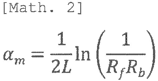
- Here, the value A denotes a proportional coefficient, the value Rf denotes the reflectivity of the low
reflective layer 9 formed on the first facet E1, the value Rb denotes the reflectivity of the highreflective layer 10 formed on the second facet E2, and the value L is the semiconductor laser length defined by the distance between the first facet E1 and the second facet E2. In the calculation, it was assumed that Rf = 0.5%, Rb = 95%, and L = 4.5 mm.FIG. 11 illustrates the result. - It is known that a consumption rate of carriers is higher in a region having a higher photon density, that is, a region having a larger optical density inside the
active region 11. It was therefore considered that, by arranging the electrical connection region in a distribution in accordance with the optical intensity distribution illustrated inFIG. 11 , it is possible to supply carriers efficiently inside theactive region 11 and thus obtain a good performance semiconductor laser device. As a result, as illustrated inFIG. 10 , thebonding wires 2 are arranged on and connected to thesecond electrode layer 13 such that thebonding wires 2 are arranged most densely on the first facet E1 side where the optical intensity is the largest and, in a portion closer to the second facet E2 side, the density of thebonding wires 2 is reduced in proportion to a reduction in the optical intensity. - With respect to the optical output power and the drive voltage, the first embodiment and the second embodiment were compared to the second conventional configuration in which
many bonding wires 2 are located only on the first facet E1 side (the configuration inFIG. 3 ).FIG. 12A and FIG. 12B illustrate the results. As a result, compared to the second conventional configuration, the drive voltage was reduced in the arrangement of thebonding wires 2 of the first embodiment in which the relationship of α > β and β > 0 are satisfied, where in the contact area between the electrical connection region and thesecond electrode layer 13, the contact area included in a half region on the first facet E1 side of the top area of thesemiconductor laser device 1 is denoted as α and the contact area included in a half region on the second facet E2 side is denoted as β. Moreover, the drive voltage is further reduced in the configuration of the second embodiment in which thebonding wires 2 are arranged such that the relationship of α > β and β > 0 are satisfied, where in the contact area between the electrical connection region and thesecond electrode layer 13, the contact area included in a half region on the first facet E1 side of the top area of thesemiconductor laser device 1 is denoted as α and the contact area included in a half region on the second facet E2 side is denoted as β, and the current density distribution in the direction connecting the first facet E1 and the second facet E2 inside theactive region 11 is close to the photon density distribution in the same direction. On the other hand, the optical output power of the first embodiment and the second embodiment was not substantially reduced compared to the optical output power of the second conventional configuration. -
FIG. 13A, FIG. 13B, and FIG. 13C illustrate results of comparison in terms of the optical output power, the drive voltage, and the electrical-optical conversion efficiency between four configurations of the first conventional configuration, the second conventional configuration, the first embodiment, and the second embodiment. - As a result, the first conventional configuration in which many bonding wires are evenly arranged has the lowest WPE, and the second conventional configuration in which many bonding wires are arranged only on the first facet side has large optical output power but has a large drive voltage resulting in a poor WPE. On the other hand, according to the configurations of the first embodiment and the second embodiment, while the optical output power is slightly lower than the second conventional configuration, the drive voltage is significantly reduced, and thus the WPE is high. In particular, the WPE was the highest in the second embodiment in which the
bonding wires 2 are arranged such that the relationship of α > β and β > 0 are satisfied, where in the contact area between the electrical connection region and thesecond electrode layer 13, the contact area included in a half region on the first facet E1 side of the top area of thesemiconductor laser device 1 is denoted as α and the contact area included in a half region on the second facet E2 side of the top area is denoted as β, and the current density distribution in the direction connecting the first facet E1 and the second facet E2 inside the active region is close to the photon density distribution in the same direction, which indicates the most preferable arrangement of the bonding wires. - As described above, to change the performance such as the optical output power, the drive voltage, the WPE, or the like of a semiconductor laser device by changing the arrangement of the electrical connection region such as bonding wires, the electrical resistance of an electrode layer to which the electrical connection region such as the bonding wires is connected is required to be sufficiently larger than the electrical connection region such as the bonding wires.
- To address this, when the electrical connection region such as the
bonding wire 2 is connected to thefirst electrode layer 23 of thesemiconductor laser device 1, for example, the thickness of thefirst electrode layer 23 formed of a metal layer of Ti/Pt/Au, an alloy layer whose primary component is Au or Zn, or the like, for example, is 2 µm or less, more preferably, 0.5 to 0.1 µm, for example. - Similarly, when the electrical connection region such as the
bonding wire 2 is connected to thesecond electrode layer 13 of thesemiconductor laser device 1, for example, the thickness of thesecond electrode layer 13 formed of an alloy layer composed of Au, Ge, and Ni or the like, for example, is 2 µm or less, more preferably, 0.5 to 0.1 µm, for example. - The present embodiment is an application example of the first embodiment. As the electrical connection region, a
bonding ribbon 32 that is an Au foil or the like shaped in a ribbon is connected to thesecond electrode layer 13 on the first facet E1 side in a configuration illustrated inFIG. 14 instead ofmany bonding wires 2 being connected in the first embodiment. Furthermore, at least one (in this example, two)bonding wire 2 is connected on the second facet E2 side. - Also in the present embodiment, the relationship of α > β is satisfied, where in the contact area between the electrical connection region described above and the
second electrode layer 13, the contact area included in a half region on the first facet E1 side of the top area of thesemiconductor laser device 1 is denoted as α and the contact area included in a half region on the second facet E2 side of the top area is denoted as β. Here, the contact area between thesecond electrode layer 13 and thebonding ribbon 32 as the electrical connection region is the area of theconnection region 33 of thebonding ribbon 32. In this area of theconnection region 33 of thebonding ribbon 32, the area included in the half region on the first facet E1 side of the top area of thesemiconductor laser device 1 corresponds to α. Furthermore, since at least one (in this example, two)bonding wire 2 is connected on the second facet E2 side of the top area of thesemiconductor laser device 1 and thus β > 0, a good performance semiconductor laser device in which an increase of WPE is realized can be obtained as with the first embodiment. - The present embodiment is an application example of the second embodiment. That is,
pads 56 are formed on the top of thesecond electrode layer 13 of thesemiconductor laser device 1, and furthermore thebonding wires 2 are connected on thepads 56 in a configuration illustrated inFIG. 15 . Each of thepads 56 is formed of Au plating or the like having a small electrical resistance, and the thickness thereof is 3 µm to 10 µm, for example. It can be considered that thepad 56 and thebonding wire 2 connected on thepad 56 have the same electric potential. Therefore, in the present embodiment, thepads 56 correspond to the electrical connection region connected to thesecond electrode layer 13 of thesemiconductor laser device 1. - Also in the present embodiment, the relationship of α > β is satisfied, where in the contact area between the electrical connection region described above and the
second electrode layer 13, the contact area included in a half region on the first facet E1 side of the top area of thesemiconductor laser device 1 is denoted as α and the contact area included in a half region on the second facet E2 side of the top area is denoted as β. Here, the contact area between the electrical connection region and thesecond electrode layer 13 corresponds to the areas of thepads 56. In the areas of thepads 56, the sum of the areas included in the half region on the first facet E1 side of the top area of thesemiconductor laser device 1 corresponds to α, and similarly, the sum of the areas included in the half region on the second facet E2 side corresponds to β. Further, at least onepad 56 is located on the second facet E2 side of the top area of thesemiconductor laser device 1, and thus β > 0. - Furthermore, in the present embodiment, the
pads 56 are formed on thesecond electrode layer 13 of thesemiconductor laser device 1 such that the current density distribution in the direction connecting the first facet E1 and the second facet E2 inside theactive region 11 of thesemiconductor laser device 1 is close to the photon density distribution in the same direction. Therefore, the present embodiment is one example of the most preferable arrangement of the electrical connection region, and a good performance semiconductor laser device in which an increase in WPE is realized can be obtained as with the second embodiment. - The present embodiment is an application example of the second embodiment. That is, a substantially
triangular pad 56 is formed on the top of thesecond electrode layer 13 of thesemiconductor laser device 1 such that the first facet E1 side of thesemiconductor laser device 1 corresponds to the base and the second facet E2 side corresponds to the vertex in a configuration as illustrated inFIG. 16 . Furthermore, thebonding wires 2 are connected onto thepad 56. Thepad 56 is formed of an Au plating or the like having a small electrical resistance, and the thickness thereof is 3 µm to 10 µm, for example. It can be considered that thepad 56 and thebonding wire 2 connected on thepad 56 have the same electric potential. Therefore, in the present embodiment, thepad 56 corresponds to the electrical connection region connected to thesecond electrode layer 13 of thesemiconductor laser device 1 as with the fourth embodiment. - Also in the present embodiment, the relationship of α > β is satisfied, where in the contact area between the electrical connection region described above and the
second electrode layer 13, the contact area included in a half region on the first facet E1 side of the top area of thesemiconductor laser device 1 is denoted as α and the contact area included in a half region on the second facet E2 side of the top area is denoted as β. Here, the contact area between the electrical connection region and thesecond electrode layer 13 corresponds to the area of thepad 56. In the present embodiment, while theintegrated pad 56 is arranged, in the area of thepad 56, the area of a portion included in the half region on the first facet E1 side of the top area of thesemiconductor laser device 1 corresponds to α, and similarly, the area of a portion included in the half region on the second facet E2 side corresponds to β. Further, thepad 56 has a substantially triangular shape such that the second facet E2 side of the top area of thesemiconductor laser device 1 corresponds to the vertex, and thus β > 0. - Furthermore, in the present embodiment, the
pad 56 is formed on thesecond electrode layer 13 of thesemiconductor laser device 1 such that the current density distribution in the direction connecting the first facet E1 and the second facet E2 inside theactive region 11 of thesemiconductor laser device 1 is close to the photon density distribution in the same direction. That is, the width of the pad 56 (the width orthogonal to the direction connecting the first facet E1 and the second facet E2) is the largest on the first facet E1 side of thesemiconductor laser device 1 and decreases as approaching the second facet E2 side in accordance with the optical intensity distribution illustrated inFIG. 11 . In such a way, by designing the shape of thepad 56 as the electrical connection region connected to thesecond electrode layer 13 of thesemiconductor laser device 1, it is possible to supply carriers efficiently inside theactive region 11. Therefore, the present embodiment is one example of the most preferable configuration of the electrical connection region, and a good performance semiconductor laser device in which an increase in WPE is realized can be obtained as with the second embodiment. - While the case where the
semiconductor laser device 1 is bonded to thesubmount 6 via the first electrode layer 23 (by junction-down bonding) and one ormore pads 56 are formed as the electrical connection region on thesecond electrode layer 13 of thesemiconductor laser device 1 has been described in the fourth embodiment and the fifth embodiment, the same advantage can be obtained even when one ormore pads 56 as illustrated in the fourth embodiment or the fifth embodiment are formed as the electrical connection region on thefirst electrode layer 23 of thesemiconductor laser device 1 and thesemiconductor laser device 1 is then bonded to thesubmount 6 via the pad(s) 56 formed on thefirst electrode layer 23. - The present embodiment is a modified example of the second embodiment. That is, as the electrical connection region, the
bonding wires 2 are arranged on and connected to thesecond electrode layer 13 of thesemiconductor laser device 1 not in the form of two lines but in the form of a single line in a configuration illustrated inFIG. 17 . - In a case of a semiconductor laser device having the optical output power around 10 mW to 2 W, for example, which injects a current around 10 mA to 3 A, for example, the bonding wires are not necessarily required to be formed in two lines. It is not preferable to connect more bonding wires than is needed to the electrode layer of the semiconductor laser device, because such connection causes disadvantages of an increase in cost of the material such as Au, an increase in process tact time, or the like.
- In the present embodiment, the relationship of α > β is satisfied, where in the contact area between the electrical connection region described above and the
second electrode layer 13, the contact area included in a half region on the first facet E1 side of the top area of thesemiconductor laser device 1 is denoted as α and the contact area included in a half region on the second facet E2 side of the top area is denoted as β, and at least onebonding wire 2 is connected on the second facet E2 side of the top area of thesemiconductor laser device 1 and thus β > 0. Furthermore, thebonding wires 2 are arranged in a form of a single line such that the current density distribution in the direction connecting the first facet E1 and the second facet E2 inside theactive region 11 of thesemiconductor laser device 1 is close to the photon density distribution in the same direction. Therefore, in a semiconductor laser device of the optical output power around 10 mW to 2 W, for example, the present embodiment is one example of the most preferable arrangement of the electrical connection region, and a good performance semiconductor laser device in which an increase in WPE is realized can be obtained. - While the case where the semiconductor laser device is bonded to the submount by junction-down bonding and the electrical connection region is connected to or formed on the second electrode layer has been described in the above embodiments, the semiconductor laser device may be bonded to the submount by junction-up bonding, and the electrical connection region may be connected to or formed on the first electrode layer.
- While the case where the optical semiconductor device is a semiconductor laser device has been described in the above embodiments, the type of the optical semiconductor device is not particularly limited. For example, the optical semiconductor device may be a semiconductor optical amplifier which is input with a laser from the second facet and outputs a laser whose optical output power is 10 mW or higher from the first facet. Further, the optical semiconductor device may be a semiconductor integrated circuit device in which a semiconductor laser device and an optical semiconductor amplifier are integrated.
- This application claims the priority from Japanese Patent Application No.
2018-025526, filed February 16, 2018 -
- 1: semiconductor laser device
- 2: bonding wire
- 4: metal layer
- 5: substrate
- 6: submount
- 7: solder
- 8: semiconductor multilayer structure
- E1: first facet
- E2: second facet
- L: semiconductor laser length
- 9: low reflective layer
- 10: high reflective layer
- 11: active region
- 12: waveguide width
- 13: second electrode layer
- 14: substrate
- 15: n-type buffer layer
- 16: n-type clad layer
- 17: n-type waveguide layer
- 18: active layer
- 18a: lower barrier layer
- 18b: quantum well layer
- 18c: upper barrier layer
- 19: p-type waveguide layer
- 20: p-type clad layer
- 21: p-type contact layer
- 22: passivation layer
- 22a: opening region
- 23: first electrode layer
- 24: connection region of bonding wire
- 32: bonding ribbon
- 33: connection region of bonding ribbon
- 56: pad
Claims (7)
- An optical semiconductor device comprising:an optical semiconductor device includinga semiconductor multilayer structure,an active region interposed between a first facet on a light emitting side and a second facet opposing to the first facet, anda first electrode layer provided on a top of the semiconductor multilayer structure and a second electrode layer provided on a bottom of the semiconductor multilayer structure; andan electrical connection region connected to at least one of the first electrode layer and the second electrode layer of the optical semiconductor device and used for injecting a current to the active region,wherein α > β and β > 0 are satisfied, where in a contact area between the electrical connection region and the optical semiconductor device, the contact area included in a half region on the first facet side in a top area of the optical semiconductor device is denoted as α, and the contact area included in a half region on the second facet side is denoted as β.
- The optical semiconductor device according to claim 1, wherein a part of the electrical connection region connected to the half region on the second facet side in a top area of the optical semiconductor device is located near the second facet.
- The optical semiconductor device according to claim 1, wherein a part of the electrical connection region connected to the half region on the second facet side in a top area of the optical semiconductor device is located in a quarter region from the second facet side.
- The optical semiconductor device according to any one of claims 1 to 3, wherein the electrical connection region is arranged and connected such that a current density distribution in a direction connecting the first facet and the second facet inside the active region is close to a photon density distribution in the same direction inside the active region.
- The optical semiconductor device according to any one of claims 1 to 4, wherein the optical semiconductor device is a semiconductor laser device in which the optical output power of a light emitting from the first facet is greater than or equal to 100 mW.
- The optical semiconductor device according to any one of claims 1 to 4, wherein the optical output power from the first facet is greater than or equal to 1 W, and the optical semiconductor device is a semiconductor laser device that oscillates the multimode laser.
- The optical semiconductor device according to any one of claims 1 to 4, wherein the optical semiconductor device is a semiconductor optical amplifier device that is inputted with a laser from the second facet and outputs, from the first facet, the optical output power is greater than or equal to 10 mW.
Applications Claiming Priority (2)
| Application Number | Priority Date | Filing Date | Title |
|---|---|---|---|
| JP2018025526 | 2018-02-16 | ||
| PCT/JP2019/005350 WO2019160039A1 (en) | 2018-02-16 | 2019-02-14 | Optical semiconductor device |
Publications (3)
| Publication Number | Publication Date |
|---|---|
| EP3754799A1 true EP3754799A1 (en) | 2020-12-23 |
| EP3754799A4 EP3754799A4 (en) | 2021-12-22 |
| EP3754799B1 EP3754799B1 (en) | 2023-06-21 |
Family
ID=67618664
Family Applications (1)
| Application Number | Title | Priority Date | Filing Date |
|---|---|---|---|
| EP19753933.1A Active EP3754799B1 (en) | 2018-02-16 | 2019-02-14 | Optical semiconductor device |
Country Status (5)
| Country | Link |
|---|---|
| US (1) | US11451008B2 (en) |
| EP (1) | EP3754799B1 (en) |
| JP (1) | JP7288425B2 (en) |
| CN (1) | CN111712979B (en) |
| WO (1) | WO2019160039A1 (en) |
Families Citing this family (2)
| Publication number | Priority date | Publication date | Assignee | Title |
|---|---|---|---|---|
| JP7420625B2 (en) * | 2020-03-30 | 2024-01-23 | 古河電気工業株式会社 | Submounts, light emitters, and optical modules |
| WO2024171718A1 (en) * | 2023-02-15 | 2024-08-22 | 株式会社フジクラ | Chip-on-submount structure |
Family Cites Families (19)
| Publication number | Priority date | Publication date | Assignee | Title |
|---|---|---|---|---|
| JPS5850790A (en) * | 1981-09-19 | 1983-03-25 | Mitsubishi Electric Corp | Photo semiconductor device |
| JP2572082B2 (en) * | 1987-10-28 | 1997-01-16 | 富士写真フイルム株式会社 | Optical semiconductor device |
| EP0477987B1 (en) * | 1990-09-28 | 1995-12-20 | Nec Corporation | Circuit and electrode arrangement for inducing flat frequency modulation response in semiconductor laser |
| US5793521A (en) * | 1992-09-21 | 1998-08-11 | Sdl Inc. | Differentially patterned pumped optical semiconductor gain media |
| JP3672272B2 (en) | 1995-04-07 | 2005-07-20 | 三菱電機株式会社 | Optical semiconductor device |
| TW289175B (en) | 1995-04-07 | 1996-10-21 | Mitsubishi Electric Corp | |
| US5757832A (en) * | 1995-04-27 | 1998-05-26 | Canon Kabushiki Kaisha | Optical semiconductor device, driving method therefor and light source and opitcal communication system using the same |
| US6181721B1 (en) | 1996-05-20 | 2001-01-30 | Sdl, Inc. | Visible wavelength, semiconductor optoelectronic device with a high power broad, significantly laterally uniform, diffraction limited output beam |
| JPH10200200A (en) * | 1997-01-06 | 1998-07-31 | Canon Inc | Surface emitting semiconductor laser |
| CN100357770C (en) * | 2001-07-30 | 2007-12-26 | 古河电气工业株式会社 | Single mode optical fiber, method of manufacturing the same, and apparatus for manufacturing the same |
| US6731427B1 (en) * | 2001-09-06 | 2004-05-04 | Onetta, Inc. | Semiconductor optical amplifier systems |
| DE602004024451D1 (en) | 2003-12-22 | 2010-01-14 | Panasonic Corp | SEMICONDUCTOR LASER ELEMENT AND LASER PROJECTOR |
| JP4570353B2 (en) * | 2003-12-26 | 2010-10-27 | 古河電気工業株式会社 | Semiconductor laser element |
| US7079310B2 (en) * | 2004-01-08 | 2006-07-18 | Chih-Hsiao Chen | Gain-clamped optical amplifier |
| US7359113B2 (en) * | 2005-02-02 | 2008-04-15 | Covega Corp. | Semiconductor optical amplifier having a non-uniform injection current density |
| GB2427752A (en) * | 2005-06-28 | 2007-01-03 | Bookham Technology Plc | High power semiconductor laser diode |
| JP5092241B2 (en) * | 2006-01-18 | 2012-12-05 | 株式会社日立製作所 | Network system |
| EP2738889B1 (en) * | 2011-12-20 | 2016-08-10 | Huawei Technologies Co., Ltd. | Laser, passive optical network system and apparatus, and method for controlling wavelength |
| JP6832567B2 (en) | 2016-08-02 | 2021-02-24 | 村角工業株式会社 | Specimen storage container |
-
2019
- 2019-02-14 CN CN201980013122.5A patent/CN111712979B/en active Active
- 2019-02-14 EP EP19753933.1A patent/EP3754799B1/en active Active
- 2019-02-14 WO PCT/JP2019/005350 patent/WO2019160039A1/en not_active Ceased
- 2019-02-14 JP JP2020500556A patent/JP7288425B2/en active Active
-
2020
- 2020-07-15 US US16/929,254 patent/US11451008B2/en active Active
Also Published As
| Publication number | Publication date |
|---|---|
| CN111712979B (en) | 2023-08-22 |
| EP3754799B1 (en) | 2023-06-21 |
| US20200366060A1 (en) | 2020-11-19 |
| WO2019160039A1 (en) | 2019-08-22 |
| US11451008B2 (en) | 2022-09-20 |
| JP7288425B2 (en) | 2023-06-07 |
| EP3754799A4 (en) | 2021-12-22 |
| JPWO2019160039A1 (en) | 2021-02-04 |
| CN111712979A (en) | 2020-09-25 |
Similar Documents
| Publication | Publication Date | Title |
|---|---|---|
| US11437780B2 (en) | Semiconductor laser device, semiconductor laser module, and welding laser light source system | |
| US8520712B2 (en) | Laser diode and method of manufacturing the same | |
| JPH11163458A (en) | Semiconductor laser device | |
| CN109417276B (en) | Semiconductor laser device, semiconductor laser module, and laser light source system for welding | |
| US20130315273A1 (en) | Integrated semiconductor laser element | |
| US20070223549A1 (en) | High-Power Optoelectronic Device with Improved Beam Quality Incorporating A Lateral Mode Filtering Section | |
| JPWO2018003335A1 (en) | Semiconductor laser device, semiconductor laser module and laser light source system for welding | |
| US11451008B2 (en) | Optical semiconductor device | |
| JP5877070B2 (en) | Semiconductor laser device | |
| US20130028283A1 (en) | High speed vertical-cavity surface-emitting laser | |
| US6996149B2 (en) | Semiconductor laser device and semiconductor laser module | |
| JP6973480B2 (en) | Laser device assembly | |
| Erbert et al. | Highly reliable 75W InGaAs/AlGaAs laser bars with over 70% conversion efficiency | |
| JPS60145687A (en) | Semiconductor laser | |
| US20130161516A1 (en) | Optical pulse tester using light emitting device | |
| CN118801210B (en) | A high-power anti-reflection semiconductor laser | |
| US20230327404A1 (en) | Inverted slab-coupled optical waveguide | |
| JPH11112096A (en) | Semiconductor laser device and optical communication system using the same | |
| KR20190137521A (en) | Laser diode structure and manufacturing method | |
| EP4668504A1 (en) | Chip-on-submount structure | |
| JP2001257417A (en) | Semiconductor laser device | |
| JP5440565B2 (en) | Group III nitride semiconductor laser, semiconductor laser device | |
| JP2001308445A (en) | Semiconductor laser device | |
| CN121726828A (en) | High-power single transverse mode side-emitting semiconductor laser and preparation method thereof | |
| EP0118671A1 (en) | Semiconductor laser device |
Legal Events
| Date | Code | Title | Description |
|---|---|---|---|
| STAA | Information on the status of an ep patent application or granted ep patent |
Free format text: STATUS: THE INTERNATIONAL PUBLICATION HAS BEEN MADE |
|
| PUAI | Public reference made under article 153(3) epc to a published international application that has entered the european phase |
Free format text: ORIGINAL CODE: 0009012 |
|
| STAA | Information on the status of an ep patent application or granted ep patent |
Free format text: STATUS: REQUEST FOR EXAMINATION WAS MADE |
|
| 17P | Request for examination filed |
Effective date: 20200714 |
|
| AK | Designated contracting states |
Kind code of ref document: A1 Designated state(s): AL AT BE BG CH CY CZ DE DK EE ES FI FR GB GR HR HU IE IS IT LI LT LU LV MC MK MT NL NO PL PT RO RS SE SI SK SM TR |
|
| AX | Request for extension of the european patent |
Extension state: BA ME |
|
| DAV | Request for validation of the european patent (deleted) | ||
| DAX | Request for extension of the european patent (deleted) | ||
| A4 | Supplementary search report drawn up and despatched |
Effective date: 20211118 |
|
| RIC1 | Information provided on ipc code assigned before grant |
Ipc: H01S 5/343 20060101ALN20211112BHEP Ipc: H01S 5/30 20060101ALN20211112BHEP Ipc: H01S 5/065 20060101ALN20211112BHEP Ipc: H01S 5/028 20060101ALN20211112BHEP Ipc: H01S 5/024 20060101ALN20211112BHEP Ipc: H01S 5/22 20060101ALI20211112BHEP Ipc: H01S 5/10 20210101ALI20211112BHEP Ipc: H01S 5/02345 20210101ALI20211112BHEP Ipc: H01S 5/50 20060101ALI20211112BHEP Ipc: H01S 5/022 20210101ALI20211112BHEP Ipc: H01S 5/042 20060101AFI20211112BHEP |
|
| RIC1 | Information provided on ipc code assigned before grant |
Ipc: H01S 5/343 20060101ALN20221130BHEP Ipc: H01S 5/30 20060101ALN20221130BHEP Ipc: H01S 5/065 20060101ALN20221130BHEP Ipc: H01S 5/028 20060101ALN20221130BHEP Ipc: H01S 5/024 20060101ALN20221130BHEP Ipc: H01S 5/22 20060101ALI20221130BHEP Ipc: H01S 5/10 20060101ALI20221130BHEP Ipc: H01S 5/02345 20210101ALI20221130BHEP Ipc: H01S 5/50 20060101ALI20221130BHEP Ipc: H01S 5/022 20060101ALI20221130BHEP Ipc: H01S 5/042 20060101AFI20221130BHEP |
|
| RIC1 | Information provided on ipc code assigned before grant |
Ipc: H01S 5/343 20060101ALN20221205BHEP Ipc: H01S 5/30 20060101ALN20221205BHEP Ipc: H01S 5/065 20060101ALN20221205BHEP Ipc: H01S 5/028 20060101ALN20221205BHEP Ipc: H01S 5/024 20060101ALN20221205BHEP Ipc: H01S 5/22 20060101ALI20221205BHEP Ipc: H01S 5/10 20060101ALI20221205BHEP Ipc: H01S 5/02345 20210101ALI20221205BHEP Ipc: H01S 5/50 20060101ALI20221205BHEP Ipc: H01S 5/022 20060101ALI20221205BHEP Ipc: H01S 5/042 20060101AFI20221205BHEP |
|
| RIC1 | Information provided on ipc code assigned before grant |
Ipc: H01S 5/343 20060101ALN20221212BHEP Ipc: H01S 5/30 20060101ALN20221212BHEP Ipc: H01S 5/065 20060101ALN20221212BHEP Ipc: H01S 5/028 20060101ALN20221212BHEP Ipc: H01S 5/024 20060101ALN20221212BHEP Ipc: H01S 5/22 20060101ALI20221212BHEP Ipc: H01S 5/10 20060101ALI20221212BHEP Ipc: H01S 5/02345 20210101ALI20221212BHEP Ipc: H01S 5/50 20060101ALI20221212BHEP Ipc: H01S 5/022 20060101ALI20221212BHEP Ipc: H01S 5/042 20060101AFI20221212BHEP |
|
| GRAP | Despatch of communication of intention to grant a patent |
Free format text: ORIGINAL CODE: EPIDOSNIGR1 |
|
| STAA | Information on the status of an ep patent application or granted ep patent |
Free format text: STATUS: GRANT OF PATENT IS INTENDED |
|
| RIC1 | Information provided on ipc code assigned before grant |
Ipc: H01S 5/343 20000101ALN20230105BHEP Ipc: H01S 5/30 20000101ALN20230105BHEP Ipc: H01S 5/065 20000101ALN20230105BHEP Ipc: H01S 5/028 20000101ALN20230105BHEP Ipc: H01S 5/024 20000101ALN20230105BHEP Ipc: H01S 5/22 20000101ALI20230105BHEP Ipc: H01S 5/10 20000101ALI20230105BHEP Ipc: H01S 5/02345 20210101ALI20230105BHEP Ipc: H01S 5/50 20000101ALI20230105BHEP Ipc: H01S 5/022 20000101ALI20230105BHEP Ipc: H01S 5/042 20000101AFI20230105BHEP |
|
| RIC1 | Information provided on ipc code assigned before grant |
Ipc: H01S 5/343 20060101ALN20230116BHEP Ipc: H01S 5/30 20060101ALN20230116BHEP Ipc: H01S 5/065 20060101ALN20230116BHEP Ipc: H01S 5/028 20060101ALN20230116BHEP Ipc: H01S 5/024 20060101ALN20230116BHEP Ipc: H01S 5/22 20060101ALI20230116BHEP Ipc: H01S 5/10 20060101ALI20230116BHEP Ipc: H01S 5/02345 20210101ALI20230116BHEP Ipc: H01S 5/50 20060101ALI20230116BHEP Ipc: H01S 5/022 20060101ALI20230116BHEP Ipc: H01S 5/042 20060101AFI20230116BHEP |
|
| INTG | Intention to grant announced |
Effective date: 20230131 |
|
| GRAS | Grant fee paid |
Free format text: ORIGINAL CODE: EPIDOSNIGR3 |
|
| GRAA | (expected) grant |
Free format text: ORIGINAL CODE: 0009210 |
|
| STAA | Information on the status of an ep patent application or granted ep patent |
Free format text: STATUS: THE PATENT HAS BEEN GRANTED |
|
| P01 | Opt-out of the competence of the unified patent court (upc) registered |
Effective date: 20230417 |
|
| AK | Designated contracting states |
Kind code of ref document: B1 Designated state(s): AL AT BE BG CH CY CZ DE DK EE ES FI FR GB GR HR HU IE IS IT LI LT LU LV MC MK MT NL NO PL PT RO RS SE SI SK SM TR |
|
| REG | Reference to a national code |
Ref country code: CH Ref legal event code: EP |
|
| REG | Reference to a national code |
Ref country code: DE Ref legal event code: R096 Ref document number: 602019031374 Country of ref document: DE |
|
| REG | Reference to a national code |
Ref country code: AT Ref legal event code: REF Ref document number: 1581600 Country of ref document: AT Kind code of ref document: T Effective date: 20230715 |
|
| REG | Reference to a national code |
Ref country code: IE Ref legal event code: FG4D |
|
| REG | Reference to a national code |
Ref country code: LT Ref legal event code: MG9D |
|
| REG | Reference to a national code |
Ref country code: NL Ref legal event code: MP Effective date: 20230621 |
|
| PG25 | Lapsed in a contracting state [announced via postgrant information from national office to epo] |
Ref country code: SE Free format text: LAPSE BECAUSE OF FAILURE TO SUBMIT A TRANSLATION OF THE DESCRIPTION OR TO PAY THE FEE WITHIN THE PRESCRIBED TIME-LIMIT Effective date: 20230621 Ref country code: NO Free format text: LAPSE BECAUSE OF FAILURE TO SUBMIT A TRANSLATION OF THE DESCRIPTION OR TO PAY THE FEE WITHIN THE PRESCRIBED TIME-LIMIT Effective date: 20230921 |
|
| REG | Reference to a national code |
Ref country code: AT Ref legal event code: MK05 Ref document number: 1581600 Country of ref document: AT Kind code of ref document: T Effective date: 20230621 |
|
| PG25 | Lapsed in a contracting state [announced via postgrant information from national office to epo] |
Ref country code: RS Free format text: LAPSE BECAUSE OF FAILURE TO SUBMIT A TRANSLATION OF THE DESCRIPTION OR TO PAY THE FEE WITHIN THE PRESCRIBED TIME-LIMIT Effective date: 20230621 Ref country code: NL Free format text: LAPSE BECAUSE OF FAILURE TO SUBMIT A TRANSLATION OF THE DESCRIPTION OR TO PAY THE FEE WITHIN THE PRESCRIBED TIME-LIMIT Effective date: 20230621 Ref country code: LV Free format text: LAPSE BECAUSE OF FAILURE TO SUBMIT A TRANSLATION OF THE DESCRIPTION OR TO PAY THE FEE WITHIN THE PRESCRIBED TIME-LIMIT Effective date: 20230621 Ref country code: LT Free format text: LAPSE BECAUSE OF FAILURE TO SUBMIT A TRANSLATION OF THE DESCRIPTION OR TO PAY THE FEE WITHIN THE PRESCRIBED TIME-LIMIT Effective date: 20230621 Ref country code: HR Free format text: LAPSE BECAUSE OF FAILURE TO SUBMIT A TRANSLATION OF THE DESCRIPTION OR TO PAY THE FEE WITHIN THE PRESCRIBED TIME-LIMIT Effective date: 20230621 Ref country code: GR Free format text: LAPSE BECAUSE OF FAILURE TO SUBMIT A TRANSLATION OF THE DESCRIPTION OR TO PAY THE FEE WITHIN THE PRESCRIBED TIME-LIMIT Effective date: 20230922 |
|
| PG25 | Lapsed in a contracting state [announced via postgrant information from national office to epo] |
Ref country code: FI Free format text: LAPSE BECAUSE OF FAILURE TO SUBMIT A TRANSLATION OF THE DESCRIPTION OR TO PAY THE FEE WITHIN THE PRESCRIBED TIME-LIMIT Effective date: 20230621 |
|
| PG25 | Lapsed in a contracting state [announced via postgrant information from national office to epo] |
Ref country code: SK Free format text: LAPSE BECAUSE OF FAILURE TO SUBMIT A TRANSLATION OF THE DESCRIPTION OR TO PAY THE FEE WITHIN THE PRESCRIBED TIME-LIMIT Effective date: 20230621 |
|
| PG25 | Lapsed in a contracting state [announced via postgrant information from national office to epo] |
Ref country code: ES Free format text: LAPSE BECAUSE OF FAILURE TO SUBMIT A TRANSLATION OF THE DESCRIPTION OR TO PAY THE FEE WITHIN THE PRESCRIBED TIME-LIMIT Effective date: 20230621 |
|
| PG25 | Lapsed in a contracting state [announced via postgrant information from national office to epo] |
Ref country code: IS Free format text: LAPSE BECAUSE OF FAILURE TO SUBMIT A TRANSLATION OF THE DESCRIPTION OR TO PAY THE FEE WITHIN THE PRESCRIBED TIME-LIMIT Effective date: 20231021 |
|
| PG25 | Lapsed in a contracting state [announced via postgrant information from national office to epo] |
Ref country code: SM Free format text: LAPSE BECAUSE OF FAILURE TO SUBMIT A TRANSLATION OF THE DESCRIPTION OR TO PAY THE FEE WITHIN THE PRESCRIBED TIME-LIMIT Effective date: 20230621 Ref country code: SK Free format text: LAPSE BECAUSE OF FAILURE TO SUBMIT A TRANSLATION OF THE DESCRIPTION OR TO PAY THE FEE WITHIN THE PRESCRIBED TIME-LIMIT Effective date: 20230621 Ref country code: RO Free format text: LAPSE BECAUSE OF FAILURE TO SUBMIT A TRANSLATION OF THE DESCRIPTION OR TO PAY THE FEE WITHIN THE PRESCRIBED TIME-LIMIT Effective date: 20230621 Ref country code: PT Free format text: LAPSE BECAUSE OF FAILURE TO SUBMIT A TRANSLATION OF THE DESCRIPTION OR TO PAY THE FEE WITHIN THE PRESCRIBED TIME-LIMIT Effective date: 20231023 Ref country code: IS Free format text: LAPSE BECAUSE OF FAILURE TO SUBMIT A TRANSLATION OF THE DESCRIPTION OR TO PAY THE FEE WITHIN THE PRESCRIBED TIME-LIMIT Effective date: 20231021 Ref country code: ES Free format text: LAPSE BECAUSE OF FAILURE TO SUBMIT A TRANSLATION OF THE DESCRIPTION OR TO PAY THE FEE WITHIN THE PRESCRIBED TIME-LIMIT Effective date: 20230621 Ref country code: EE Free format text: LAPSE BECAUSE OF FAILURE TO SUBMIT A TRANSLATION OF THE DESCRIPTION OR TO PAY THE FEE WITHIN THE PRESCRIBED TIME-LIMIT Effective date: 20230621 Ref country code: CZ Free format text: LAPSE BECAUSE OF FAILURE TO SUBMIT A TRANSLATION OF THE DESCRIPTION OR TO PAY THE FEE WITHIN THE PRESCRIBED TIME-LIMIT Effective date: 20230621 Ref country code: AT Free format text: LAPSE BECAUSE OF FAILURE TO SUBMIT A TRANSLATION OF THE DESCRIPTION OR TO PAY THE FEE WITHIN THE PRESCRIBED TIME-LIMIT Effective date: 20230621 |
|
| PG25 | Lapsed in a contracting state [announced via postgrant information from national office to epo] |
Ref country code: PL Free format text: LAPSE BECAUSE OF FAILURE TO SUBMIT A TRANSLATION OF THE DESCRIPTION OR TO PAY THE FEE WITHIN THE PRESCRIBED TIME-LIMIT Effective date: 20230621 |
|
| REG | Reference to a national code |
Ref country code: DE Ref legal event code: R097 Ref document number: 602019031374 Country of ref document: DE |
|
| PLBE | No opposition filed within time limit |
Free format text: ORIGINAL CODE: 0009261 |
|
| STAA | Information on the status of an ep patent application or granted ep patent |
Free format text: STATUS: NO OPPOSITION FILED WITHIN TIME LIMIT |
|
| PG25 | Lapsed in a contracting state [announced via postgrant information from national office to epo] |
Ref country code: DK Free format text: LAPSE BECAUSE OF FAILURE TO SUBMIT A TRANSLATION OF THE DESCRIPTION OR TO PAY THE FEE WITHIN THE PRESCRIBED TIME-LIMIT Effective date: 20230621 |
|
| PG25 | Lapsed in a contracting state [announced via postgrant information from national office to epo] |
Ref country code: SI Free format text: LAPSE BECAUSE OF FAILURE TO SUBMIT A TRANSLATION OF THE DESCRIPTION OR TO PAY THE FEE WITHIN THE PRESCRIBED TIME-LIMIT Effective date: 20230621 |
|
| 26N | No opposition filed |
Effective date: 20240322 |
|
| PG25 | Lapsed in a contracting state [announced via postgrant information from national office to epo] |
Ref country code: SI Free format text: LAPSE BECAUSE OF FAILURE TO SUBMIT A TRANSLATION OF THE DESCRIPTION OR TO PAY THE FEE WITHIN THE PRESCRIBED TIME-LIMIT Effective date: 20230621 Ref country code: IT Free format text: LAPSE BECAUSE OF FAILURE TO SUBMIT A TRANSLATION OF THE DESCRIPTION OR TO PAY THE FEE WITHIN THE PRESCRIBED TIME-LIMIT Effective date: 20230621 |
|
| PG25 | Lapsed in a contracting state [announced via postgrant information from national office to epo] |
Ref country code: MC Free format text: LAPSE BECAUSE OF FAILURE TO SUBMIT A TRANSLATION OF THE DESCRIPTION OR TO PAY THE FEE WITHIN THE PRESCRIBED TIME-LIMIT Effective date: 20230621 |
|
| REG | Reference to a national code |
Ref country code: CH Ref legal event code: PL |
|
| PG25 | Lapsed in a contracting state [announced via postgrant information from national office to epo] |
Ref country code: LU Free format text: LAPSE BECAUSE OF NON-PAYMENT OF DUE FEES Effective date: 20240214 |
|
| PG25 | Lapsed in a contracting state [announced via postgrant information from national office to epo] |
Ref country code: CH Free format text: LAPSE BECAUSE OF NON-PAYMENT OF DUE FEES Effective date: 20240229 |
|
| GBPC | Gb: european patent ceased through non-payment of renewal fee |
Effective date: 20240214 |
|
| PG25 | Lapsed in a contracting state [announced via postgrant information from national office to epo] |
Ref country code: LU Free format text: LAPSE BECAUSE OF NON-PAYMENT OF DUE FEES Effective date: 20240214 Ref country code: CH Free format text: LAPSE BECAUSE OF NON-PAYMENT OF DUE FEES Effective date: 20240229 |
|
| PG25 | Lapsed in a contracting state [announced via postgrant information from national office to epo] |
Ref country code: BG Free format text: LAPSE BECAUSE OF FAILURE TO SUBMIT A TRANSLATION OF THE DESCRIPTION OR TO PAY THE FEE WITHIN THE PRESCRIBED TIME-LIMIT Effective date: 20230621 |
|
| PG25 | Lapsed in a contracting state [announced via postgrant information from national office to epo] |
Ref country code: BG Free format text: LAPSE BECAUSE OF FAILURE TO SUBMIT A TRANSLATION OF THE DESCRIPTION OR TO PAY THE FEE WITHIN THE PRESCRIBED TIME-LIMIT Effective date: 20230621 |
|
| REG | Reference to a national code |
Ref country code: BE Ref legal event code: MM Effective date: 20240229 |
|
| PG25 | Lapsed in a contracting state [announced via postgrant information from national office to epo] |
Ref country code: BE Free format text: LAPSE BECAUSE OF NON-PAYMENT OF DUE FEES Effective date: 20240229 |
|
| PG25 | Lapsed in a contracting state [announced via postgrant information from national office to epo] |
Ref country code: GB Free format text: LAPSE BECAUSE OF NON-PAYMENT OF DUE FEES Effective date: 20240214 |
|
| PG25 | Lapsed in a contracting state [announced via postgrant information from national office to epo] |
Ref country code: FR Free format text: LAPSE BECAUSE OF NON-PAYMENT OF DUE FEES Effective date: 20240229 |
|
| PG25 | Lapsed in a contracting state [announced via postgrant information from national office to epo] |
Ref country code: IE Free format text: LAPSE BECAUSE OF NON-PAYMENT OF DUE FEES Effective date: 20240214 |
|
| PG25 | Lapsed in a contracting state [announced via postgrant information from national office to epo] |
Ref country code: IE Free format text: LAPSE BECAUSE OF NON-PAYMENT OF DUE FEES Effective date: 20240214 Ref country code: GB Free format text: LAPSE BECAUSE OF NON-PAYMENT OF DUE FEES Effective date: 20240214 Ref country code: FR Free format text: LAPSE BECAUSE OF NON-PAYMENT OF DUE FEES Effective date: 20240229 Ref country code: BE Free format text: LAPSE BECAUSE OF NON-PAYMENT OF DUE FEES Effective date: 20240229 |
|
| PG25 | Lapsed in a contracting state [announced via postgrant information from national office to epo] |
Ref country code: CY Free format text: LAPSE BECAUSE OF FAILURE TO SUBMIT A TRANSLATION OF THE DESCRIPTION OR TO PAY THE FEE WITHIN THE PRESCRIBED TIME-LIMIT; INVALID AB INITIO Effective date: 20190214 |
|
| PG25 | Lapsed in a contracting state [announced via postgrant information from national office to epo] |
Ref country code: HU Free format text: LAPSE BECAUSE OF FAILURE TO SUBMIT A TRANSLATION OF THE DESCRIPTION OR TO PAY THE FEE WITHIN THE PRESCRIBED TIME-LIMIT; INVALID AB INITIO Effective date: 20190214 |
|
| PG25 | Lapsed in a contracting state [announced via postgrant information from national office to epo] |
Ref country code: TR Free format text: LAPSE BECAUSE OF FAILURE TO SUBMIT A TRANSLATION OF THE DESCRIPTION OR TO PAY THE FEE WITHIN THE PRESCRIBED TIME-LIMIT Effective date: 20230621 |
|
| PGFP | Annual fee paid to national office [announced via postgrant information from national office to epo] |
Ref country code: DE Payment date: 20251230 Year of fee payment: 8 |