EP3754731A1 - Method for local removal of semiconductor wires - Google Patents
Method for local removal of semiconductor wires Download PDFInfo
- Publication number
- EP3754731A1 EP3754731A1 EP19315044.8A EP19315044A EP3754731A1 EP 3754731 A1 EP3754731 A1 EP 3754731A1 EP 19315044 A EP19315044 A EP 19315044A EP 3754731 A1 EP3754731 A1 EP 3754731A1
- Authority
- EP
- European Patent Office
- Prior art keywords
- layer
- composite layer
- semiconductor
- previous
- semiconductor wires
- Prior art date
- Legal status (The legal status is an assumption and is not a legal conclusion. Google has not performed a legal analysis and makes no representation as to the accuracy of the status listed.)
- Withdrawn
Links
Images


Classifications
-
- H—ELECTRICITY
- H01—ELECTRIC ELEMENTS
- H01L—SEMICONDUCTOR DEVICES NOT COVERED BY CLASS H10
- H01L33/00—Semiconductor devices with at least one potential-jump barrier or surface barrier specially adapted for light emission; Processes or apparatus specially adapted for the manufacture or treatment thereof or of parts thereof; Details thereof
- H01L33/02—Semiconductor devices with at least one potential-jump barrier or surface barrier specially adapted for light emission; Processes or apparatus specially adapted for the manufacture or treatment thereof or of parts thereof; Details thereof characterised by the semiconductor bodies
- H01L33/16—Semiconductor devices with at least one potential-jump barrier or surface barrier specially adapted for light emission; Processes or apparatus specially adapted for the manufacture or treatment thereof or of parts thereof; Details thereof characterised by the semiconductor bodies with a particular crystal structure or orientation, e.g. polycrystalline, amorphous or porous
- H01L33/18—Semiconductor devices with at least one potential-jump barrier or surface barrier specially adapted for light emission; Processes or apparatus specially adapted for the manufacture or treatment thereof or of parts thereof; Details thereof characterised by the semiconductor bodies with a particular crystal structure or orientation, e.g. polycrystalline, amorphous or porous within the light emitting region
-
- H—ELECTRICITY
- H01—ELECTRIC ELEMENTS
- H01L—SEMICONDUCTOR DEVICES NOT COVERED BY CLASS H10
- H01L33/00—Semiconductor devices with at least one potential-jump barrier or surface barrier specially adapted for light emission; Processes or apparatus specially adapted for the manufacture or treatment thereof or of parts thereof; Details thereof
- H01L33/005—Processes
- H01L33/0062—Processes for devices with an active region comprising only III-V compounds
- H01L33/0075—Processes for devices with an active region comprising only III-V compounds comprising nitride compounds
-
- H—ELECTRICITY
- H01—ELECTRIC ELEMENTS
- H01L—SEMICONDUCTOR DEVICES NOT COVERED BY CLASS H10
- H01L33/00—Semiconductor devices with at least one potential-jump barrier or surface barrier specially adapted for light emission; Processes or apparatus specially adapted for the manufacture or treatment thereof or of parts thereof; Details thereof
- H01L33/005—Processes
- H01L33/0095—Post-treatment of devices, e.g. annealing, recrystallisation or short-circuit elimination
-
- H—ELECTRICITY
- H01—ELECTRIC ELEMENTS
- H01L—SEMICONDUCTOR DEVICES NOT COVERED BY CLASS H10
- H01L33/00—Semiconductor devices with at least one potential-jump barrier or surface barrier specially adapted for light emission; Processes or apparatus specially adapted for the manufacture or treatment thereof or of parts thereof; Details thereof
- H01L33/02—Semiconductor devices with at least one potential-jump barrier or surface barrier specially adapted for light emission; Processes or apparatus specially adapted for the manufacture or treatment thereof or of parts thereof; Details thereof characterised by the semiconductor bodies
- H01L33/04—Semiconductor devices with at least one potential-jump barrier or surface barrier specially adapted for light emission; Processes or apparatus specially adapted for the manufacture or treatment thereof or of parts thereof; Details thereof characterised by the semiconductor bodies with a quantum effect structure or superlattice, e.g. tunnel junction
- H01L33/06—Semiconductor devices with at least one potential-jump barrier or surface barrier specially adapted for light emission; Processes or apparatus specially adapted for the manufacture or treatment thereof or of parts thereof; Details thereof characterised by the semiconductor bodies with a quantum effect structure or superlattice, e.g. tunnel junction within the light emitting region, e.g. quantum confinement structure or tunnel barrier
-
- H—ELECTRICITY
- H01—ELECTRIC ELEMENTS
- H01L—SEMICONDUCTOR DEVICES NOT COVERED BY CLASS H10
- H01L33/00—Semiconductor devices with at least one potential-jump barrier or surface barrier specially adapted for light emission; Processes or apparatus specially adapted for the manufacture or treatment thereof or of parts thereof; Details thereof
- H01L33/02—Semiconductor devices with at least one potential-jump barrier or surface barrier specially adapted for light emission; Processes or apparatus specially adapted for the manufacture or treatment thereof or of parts thereof; Details thereof characterised by the semiconductor bodies
- H01L33/20—Semiconductor devices with at least one potential-jump barrier or surface barrier specially adapted for light emission; Processes or apparatus specially adapted for the manufacture or treatment thereof or of parts thereof; Details thereof characterised by the semiconductor bodies with a particular shape, e.g. curved or truncated substrate
- H01L33/24—Semiconductor devices with at least one potential-jump barrier or surface barrier specially adapted for light emission; Processes or apparatus specially adapted for the manufacture or treatment thereof or of parts thereof; Details thereof characterised by the semiconductor bodies with a particular shape, e.g. curved or truncated substrate of the light emitting region, e.g. non-planar junction
-
- H—ELECTRICITY
- H01—ELECTRIC ELEMENTS
- H01L—SEMICONDUCTOR DEVICES NOT COVERED BY CLASS H10
- H01L2933/00—Details relating to devices covered by the group H01L33/00 but not provided for in its subgroups
- H01L2933/0008—Processes
- H01L2933/0016—Processes relating to electrodes
-
- H—ELECTRICITY
- H01—ELECTRIC ELEMENTS
- H01L—SEMICONDUCTOR DEVICES NOT COVERED BY CLASS H10
- H01L2933/00—Details relating to devices covered by the group H01L33/00 but not provided for in its subgroups
- H01L2933/0008—Processes
- H01L2933/0033—Processes relating to semiconductor body packages
- H01L2933/005—Processes relating to semiconductor body packages relating to encapsulations
-
- H—ELECTRICITY
- H01—ELECTRIC ELEMENTS
- H01L—SEMICONDUCTOR DEVICES NOT COVERED BY CLASS H10
- H01L33/00—Semiconductor devices with at least one potential-jump barrier or surface barrier specially adapted for light emission; Processes or apparatus specially adapted for the manufacture or treatment thereof or of parts thereof; Details thereof
- H01L33/005—Processes
- H01L33/0062—Processes for devices with an active region comprising only III-V compounds
- H01L33/0066—Processes for devices with an active region comprising only III-V compounds with a substrate not being a III-V compound
- H01L33/007—Processes for devices with an active region comprising only III-V compounds with a substrate not being a III-V compound comprising nitride compounds
Definitions
- the invention concerns the field of semiconductor technologies. It may relate more particularly to the manufacture of components based on small semiconductor wires having typically a diameter ranging from few tens nanometers to some micrometers.
- the invention can be worthily implemented in the manufacturing of wires- or nanowires-based light emitting diode (W-LED or NW-LED).
- SW semiconductor wires
- such 3D arrays may improve the overall efficiency of optoelectronics devices such as LED, which require good crystal quality for light emission, as well as good optical properties for light extraction.
- a plurality of 3D arrays of SW has to be integrated on a wafer.
- a first solution consists in growing locally the SW arrays on each chip or LED of the wafer, by masking areas where SW are unwanted.
- a second solution consists in growing SW all over the wafer, then removing SW from areas where SW are unwanted. Such a solution is called Wiresea growth concept.
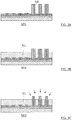
- EP 2936571 B1 discloses methods for locally removing SW from a Wiresea growth, as illustrated in figures 1A-1E .
- the Wiresea growth can typically be achieved using a stack 10 comprising a substrate 11, a two-dimensional nucleation layer 12 and a growth masking layer 13, also referred as SAG layer for "Selective Area Growth” layer.
- SW 21 are grown from the nucleation layer 12 through apertures in the SAG layer 13, forming a single SW array 20 regularly distributed on the stack 10 all over the wafer ( figure 1A ).
- a protective photoresist layer 30a is first deposited on the single SW array 20 ( figure 1B ).
- a patterning of the protective photoresist layer 30a is then performed by conventional lithography, to leave areas free of protective layer 30a ( figure 1C ).
- SW 21 are removed from these areas free of protective layer 30a using either a wet etching process, a dry etching process, or a mechanical action to break the SW.
- the present invention is intended to overcome at least partially some of the aforementioned drawbacks.
- an object of the present invention is a method for local removal of semiconductor wires which allows the effective removal of SW while maintaining the integrity of the underlying layer.
- Another object of the present invention is a method for local removal of semiconductor wires which reduces the roughness of areas where SW are removed.
- the invention provides a method for local removal of semiconductor wires comprising the following steps :
- This method is advantageously designed to achieve a single etching step of the exposed regions of the composite layer with a selectivity S semicon :S encaps around 1:1.
- the SW are etched at about the same etching rate as the encapsulation layer in the exposed regions.
- the top surface of the underlying growth masking layer is thus always protected during the etching step. It prevents any damages of the underlying layer.
- the stop of the etching step can be controlled precisely, so as to obtain a thin residual composite layer.
- the SW are effectively removed in the exposed regions, while the surface roughness of the exposed regions after etching is drastically decreased compared to prior art methods.
- the effective removal of the SW is thus not depending on the height of the SW to be removed.
- the SW to be removed often have height variations and an overetch step is then required in prior art process.
- Such an overetch step contributes to partial etching of the underlying layer.
- forming a composite layer prior to a single etching step of said composite layer prevents from an overetch of the SW, while ensuring effective removal of the SW.
- Further removal of the encapsulating material may be performed, so as to free the SW in the regions protected by the hard mask. In the exposed regions, removing the encapsulating material in the residual composite layer may result in regularly distributed small SW residues of controlled height.
- SW residues are suitable for further manufacturing steps such as forming a dielectric collar at the base of the SW, unlike the residues obtained randomly by other prior art methods.
- the method according to the invention is therefore simpler than known methods for local removal of SW. It is also more efficient to remove SW while protecting underlying layers.
- Another object of the present invention is a method for manufacturing of semiconductor wires-based light emitting diode (SW-LED) which comprises the method claimed above.
- the overall SW-LED manufacturing method is then cost effective.
- the thickness of the encapsulating layer is greater than or equal to the height of a highest semiconductor wire of the semiconductor wires.
- the composite layer is bulk.
- the stack of layers comprises a nucleation layer in between the substrate and the growth masking layer, said semiconductor wires being at least partially grown from the nucleation layer through the growth masking layer.
- the semiconductor-based material is a GaN-based material.
- the encapsulating material is chosen among SiO2, SiN, SiON, or a flowable oxide.
- the anisotropic etching is performed using a plasma comprising chlorinated species, preferably an argon/chlorine-based plasma.
- the semiconductor wires have an average height between 1 ⁇ m and 15 ⁇ m and an average diameter between 0.1 ⁇ m and 2 ⁇ m.
- the encapsulation layer is formed by spin coating.
- the encapsulation layer is deposited by a deposition technique among plasma-enhanced chemical vapor deposition (PECVD), sub-atmospheric chemical vapor deposition (SACVD), low pressure chemical vapor deposition (LPCVD).
- PECVD plasma-enhanced chemical vapor deposition
- SACVD sub-atmospheric chemical vapor deposition
- LPCVD low pressure chemical vapor deposition
- the composite layer is planarized before patterning the hard mask.
- the hard mask and the encapsulating material are removed after stopping the anisotropic etching of the composite layer, so as to leave regions without semiconductor wires in place of the residual composite layer, and regions with semiconductor wires in place of the composite layer.
- the local SW removal method is in particular dedicated to the manufacture of SW-based optoelectronic devices, in particular LEDs.
- a LED typically includes p- and n-doped regions in relation with an active region where the light is emitted.
- the relative arrangement of a third layer between a first layer and a second layer does not necessarily mean that the layers are in direct contact with each other, but means that the third layer is either in direct contact with the first and second layers or separated from each other by at least one other layer or at least one other element.
- a p-doping includes all doping by positive charge carriers regardless of the concentration of dopants.
- a p-doping can be defined as a p, p+ or p++ doping.
- an n-doping includes all doping by negative charge carriers regardless of the concentration of dopants.
- an n-doping can be defined as an n, n+ or n++ doping.
- a device, a substrate, a layer, a SW, "based" on a material M means a device, a substrate, a layer, a SW comprising this material M only or this material M and possibly other materials, for example alloying elements, impurities or doping elements.
- a gallium nitride (GaN) SW may include gallium nitride (GaN or i-GaN) and/or doped gallium nitride (p-GaN, n-GaN) and/or gallium-indium nitride (InGaN) and/or gallium-aluminium nitride (AIGaN).
- depth, height and thickness are taken perpendicularly to a basal plane of the substrate.
- thickness for a layer, height for a SW, and depth for an etching for example.
- a direction substantially normal to a plane means a direction with an angle of 90 ⁇ 10° to the plane.
- SEM scanning electron microscopy
- TEM transmission electron microscopy
- a cross-sectional observation at a contact pad may determine whether there are SW residues having about the same height at the base of said contact pad, and whether these SW residues originate from SW previously grown through a SAG layer.
- Another characteristic result of the method according to the invention is a preserved SAG layer surface.
- SW 21 are preferably grown on a planar stack 10 of layers 12, 13 which lie on a substrate 11.
- the substrate 11 may be made of silicon, GaN or sapphire.
- Each layer 12, 13 of the stack 10 extend in a basal plane and the stack 10 is formed in a direction normal to the basal plane ( Figure 2A ).
- the stack 10 may include a two-dimensional (2D) nucleation layer 12 overlaid by a growth masking layer hereafter referred as Selective Area Growth (SAG) layer 13.
- 2D two-dimensional
- SAG Selective Area Growth
- Both 2D nucleation layer 12 and SAG layer 13 are preferably directly in contact to each other.
- the 2D nucleation layer 12 may be made of (Al)(In)(Ga)N, or of tantalum, of tantalum nitride, of niobium, of niobium nitride, of titanium, of titanium nitride, of hafnium, of hafnium nitride, of boron, of boron nitride, of magnesium, of magnesium nitride, of tungsten, of tungsten nitride, or of a combination thereof.
- the 2D nucleation layer 12 may have a thickness in the range 5 nm to 50 nm, typically 25 nm.
- the SAG layer 13 may be made of SiN, SiO2, SiON, HfO2, HfN, Sc2O3, ScN, Mg2O3 or other dielectric materials.
- the SAG layer 13 may have a thickness in the range 20 nm to 200 nm, typically 100 nm.
- Holes or apertures are regularly distributed, for example in a pitch of 5 ⁇ m, but can be any pitch sizes between 100 nm to 100 ⁇ m throughout the SAG layer 13 so as to expose the underlying 2D nucleation layer 12.
- These holes have a diameter ranging from some tens of nanometers to some micrometers, for example about 0.5 ⁇ m.
- These holes are designed to assist a local growth of SW 21 from the nucleation layer 12.
- SW 21 can be grown by different growth techniques depending on the desired internal structure of the SW 21.
- the internal structure may be a longitudinal structure or a radial structure.
- SW 21 having the longitudinal structure can be grown by preferably by Molecular Beam Epitaxy (MBE) or by metal organic chemical vapour deposition (MOCVD) or remote plasma chemical vapour deposition (RP-CVD) or HVPE (Halide Vapor Phase Epitaxy or Hydride Vapour Phase Epitaxy).
- MBE Molecular Beam Epitaxy
- MOCVD metal organic chemical vapour deposition
- RP-CVD remote plasma chemical vapour deposition
- HVPE Hydrode Vapor Phase Epitaxy or Hydride Vapour Phase Epitaxy
- such a longitudinal structure may include p-GaN and n-GaN regions arranged according to the direction normal to the basal plane, with InGaN quantum wells in between.
- SW 21 having the radial structure can be grown by Metal-Organic Chemical Vapour Deposition (MOCVD), or by Metal-Organic Vapour Phase Epitaxy (MOVPE), or by Hydride Vapour Phase Epitaxy (HVPE), or by Molecular Beam Epitaxy (MBE).
- MOCVD Metal-Organic Chemical Vapour Deposition
- MOVPE Metal-Organic Vapour Phase Epitaxy
- HVPE Hydride Vapour Phase Epitaxy
- MBE Molecular Beam Epitaxy
- such a radial structure may include p-GaN, InGaN and n-GaN regions concentrically arranged around an axis normal to the basal plane.
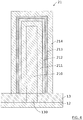
- Figure 4 shows a particular arrangement for such a radial structure.
- SW 21 can include the following sequence of regions or layers, from the inside to the outside of the SW in a radial direction:
- the core 210 of the SW 21 is first grown, for instance by MOCVD, through the holes 130 of the SAG layer 13. Then, layers 211, 212, 213, 214 may be successively grown on one another so as to form a radial structure, preferably as illustrated in figure 4 .
- SW 21 are illustrated in the following with a simple core-shell structure, regardless of the effective number of layers in the radial structure. It has also to be understood that this representation may also correspond to a longitudinal structure, if compatible.
- the single SW array 20 is first encapsulated 200 with an encapsulating material, as illustrated in figure 2B .
- the encapsulating material may be made of SiO2, SiON, SiN, BCB (Benzocyclobutene), poly methyl methacrylate (PMMA), or any form of epoxy, resin or dielectric materials.
- the encapsulating material may also be deposited by sub-atmospheric chemical vapor deposition (SACVD) or low pressure chemical vapor deposition (LPCVD).
- SACVD sub-atmospheric chemical vapor deposition
- LPCVD low pressure chemical vapor deposition
- the encapsulation layer 30b may be formed by spin-coating, for instance from a Flowable Oxide (FOx) or a spin-on glass, followed by annealing. These techniques are well known.
- FOx Flowable Oxide
- annealing annealing
- the thickness of the encapsulation layer 30b is preferably greater than or equal to the height of the semiconductor wires 21. In the case where SW 21 have different height to each other, the thickness of the encapsulation layer 30b is preferably greater than or equal to the highest SW 21.
- a composite layer 20b comprising both encapsulating material and semiconductor material is thus obtained.
- the composite layer 20b is preferably bulk, with no or few porosity within.
- the top surface of the composite layer 20b may be planarized, for instance by Chemical Mechanical Polishing (CMP), in order to get a flat top surface of the composite layer 20b.
- CMP Chemical Mechanical Polishing
- a low surface roughness preferably a peak-to-valley roughness lower than 100 nm, advantageously prevents over-etching during the subsequent etching of the composite layer 20b.
- a hard mask 40 is patterned 300 on the composite layer 20b, so as to protect regions of the composite layer 20b where SW 21 have to be kept and so as to expose regions of the composite layer 20b where SW 21 have to be removed ( figure 2C ).
- the regions of the composite layer 20b where SW 21 have to be removed may typically correspond to bonding pad regions and/or to chip trimming regions of LED.
- the regions of the composite layer 20b where SW 21 have to be kept may typically correspond to active regions of LED.
- a single etching step of the exposed regions of the composite layer 20b is then performed 400.
- Such a single etching step is preferably anisotropic and has a selectivity S semicon :S encaps between semiconductor-based material and encapsulating material such as 0.9:1 ⁇ S semicon :S encaps ⁇ 1.1:1.
- the selectivity S semicon :S encaps is preferably about 1:1 (one by one).
- the single etching step preferably consists in a dry etching performed by plasma, for instance by Reactive-Ion Etching (RIE).
- RIE Reactive-Ion Etching
- a Capacitively Coupled Plasma (CCP) reactor or an Inductively Coupled Plasma (ICP) reactor may be used.
- GaN-based SW 21 encapsulated in SiO2 a selectivity GaN:SiO2 about 1:1 may be obtained using an argon/chlorine-based plasma.
- a selectivity GaN:SiO2 about 1:1 may also be obtained using low pressure Cl2/BCl3 inductively coupled plasmas, as described in the document " S. Zhuo et al., Dry etching characteristics of GaN using Cl2/BCl3 inductively coupled plasmas, Applied Surface Science, 905-910 (2010 )".
- the anisotropic etching of the composite layer 20b is preferably performed so as to leave a thin residual composite layer 20c having a thickness h lower than 500 nm, and preferably lower than 200 nm ( figure 2D ).
- This thin residual composite layer 20c prevents over-etching.
- the underlying SAG layer 13 is thus protected.
- the encapsulating material can then be removed 500, for instance by wet etching, in order to free the SW 21 in the protected regions of the composite layer 20b, as illustrated in figure 2E .
- SiO2 or FOx encapsulating material this can be achieved using typically a wet chemistry solution based on hydrofluoric acid HF.
- a good selectivity etchant against the SAG layer is necessary, otherwise areas where SW have been etched will need to be patterned or masked to prevent parasitic SAG etching.
- SW residues 22 coming from the residual composite layer 20c may persist after such a wet etching. These SW residues 22 are substantially composed of the same layers as the SW 21 at their base.
- SW residues 22 all have about the same height h with h ⁇ 500 nm, and preferably h ⁇ 200 nm. Their diameters are close to the diameters of the SW 21 at their base.
- SW residues 22 it is important to have such a controlled height h in a reproducible way. Subsequent manufacturing steps can further be adjusted in accordance with the SW residues 22. The reproducibility of the overall manufacturing process is improved.
- figures 3A to 3E describe further steps typically involved in manufacturing SW-based LED.
- a conformal dielectric layer 50 may be deposited 501 ( figure 3A ).
- a masking layer 51 is then deposited 502, for instance by spin-coating, in order to protect a lower part of the SW 21 while exposing an upper part of the SW 21 ( figure 3B ).
- the thickness of the masking layer 51 is chosen in such a way that the upper part of the SW 21 is at least 500 nm high.
- An isotropic etching is then performed 503 in order to remove the exposed part of the dielectric layer 50 surrounding the upper part of the SW 21 ( figure 3C ).
- the masking layer 51 is then removed 504 ( figure 3D ).
- a dielectric collar 50a surrounding the lower part of the SW 21 is thus obtained, as well as a dielectric layer 50b covering the SW residues 22.
- Transparent Conductive Oxide (TCO) layer 52 and metallic pad contact 53 may then be deposited 505, so as to form a SW-based LED ( figure 3E ).
- the TCO and pad contact are thus isolated from the SW residues 22 and from the substrate 11, while connecting the exposed upper part of the SW 21.
Abstract
The invention concerns a method for local removal of semiconductor wires (SW) 21 comprising the following steps:
- Provide a stack 10 of layers 11, 12, 13 comprising at least a substrate 11, a nucleation layer 12, a growth masking layer 13, and a layer 20 comprising SW 21 being grown from the nucleation layer through the growth masking layer,
- Encapsulate the SW with an encapsulation layer 30b so as to form a composite layer 20b comprising SW and encapsulating material,
- Pattern a hard mask 40 on the composite layer, so as to expose regions of the composite layer,
- Perform anisotropic etching of the composite layer in the exposed regions, the anisotropic etching having a selectivity Ssemicon:Sencaps between semiconductor-based material and encapsulating material such as 0.9:1 < Ssemicon:Sencaps <1.1:1.
Description
- The invention concerns the field of semiconductor technologies. It may relate more particularly to the manufacture of components based on small semiconductor wires having typically a diameter ranging from few tens nanometers to some micrometers. The invention can be worthily implemented in the manufacturing of wires- or nanowires-based light emitting diode (W-LED or NW-LED).
- In the field of semiconductor technologies, three-dimensional arrays of semiconductor wires (SW) are considered as promising alternatives to two-dimensional planar semiconductor structures.
- In particular, such 3D arrays may improve the overall efficiency of optoelectronics devices such as LED, which require good crystal quality for light emission, as well as good optical properties for light extraction.
- For manufacturing cost issues, a plurality of 3D arrays of SW has to be integrated on a wafer.
- A first solution consists in growing locally the SW arrays on each chip or LED of the wafer, by masking areas where SW are unwanted.
- Such a solution often leads to inhomogeneity and/or discontinuities in SW arrays, typically due to growth perturbations at the edges of masked areas. This eventually affects the SW-based devices.
- A second solution consists in growing SW all over the wafer, then removing SW from areas where SW are unwanted. Such a solution is called Wiresea growth concept.
- The document
EP 2936571 B1 discloses methods for locally removing SW from a Wiresea growth, as illustrated infigures 1A-1E . - The Wiresea growth can typically be achieved using a
stack 10 comprising asubstrate 11, a two-dimensional nucleation layer 12 and agrowth masking layer 13, also referred as SAG layer for "Selective Area Growth" layer. -
SW 21 are grown from thenucleation layer 12 through apertures in theSAG layer 13, forming asingle SW array 20 regularly distributed on thestack 10 all over the wafer (figure 1A ). - In order to remove
SW 21 from areas where SW are unwanted, aprotective photoresist layer 30a is first deposited on the single SW array 20 (figure 1B ). - A patterning of the
protective photoresist layer 30a is then performed by conventional lithography, to leave areas free ofprotective layer 30a (figure 1C ). - Then,
SW 21 are removed from these areas free ofprotective layer 30a using either a wet etching process, a dry etching process, or a mechanical action to break the SW. - Wet and dry etching process result in
partial etching 132 of the underlying layer, typically theSAG layer 13, from the exposed surface 131 (figure 1D ). - Ultimately, such etching process can also damage the
nucleation layer 12. - Mechanical action to break the SW is difficult to control and generally results in a partial removal of SW (
figure 1E ). - In any case, a rough surface unsuitable for reproducible manufacturing conditions is obtained in the areas where SW are etched or broken.
- The present invention is intended to overcome at least partially some of the aforementioned drawbacks.
- More precisely, an object of the present invention is a method for local removal of semiconductor wires which allows the effective removal of SW while maintaining the integrity of the underlying layer.
- Another object of the present invention is a method for local removal of semiconductor wires which reduces the roughness of areas where SW are removed.
- The other objects, characteristics and advantages of the present invention will appear in the examination of the following description and accompanying drawings. It is to be understood that other benefits may be incorporated.
- To achieve these objectives, the invention provides a method for local removal of semiconductor wires comprising the following steps :
- Provide a stack of layers comprising at least a substrate, a growth masking layer, and a layer comprising semiconductor wires in a semiconductor-based material,
- Encapsulate the semiconductor wires with an encapsulation layer in an encapsulating material, so as to form a composite layer comprising semiconductor wires and encapsulating material,
- Pattern a hard mask on the composite layer, so as to expose regions of the composite layer,
- Perform anisotropic etching of the composite layer in the exposed regions, the anisotropic etching having a selectivity Ssemicon:Sencaps between semiconductor-based material and encapsulating material such as 0.9:1 < Ssemicon:Sencaps <1.1:1,
- Stop the anisotropic etching of the composite layer so as to leave a residual composite layer having a thickness between 0 nm and 500 nm, preferably between 0 nm and 200 nm, and more preferably between 0 nm and 100 nm.
- This method is advantageously designed to achieve a single etching step of the exposed regions of the composite layer with a selectivity Ssemicon:Sencaps around 1:1.
- In this way, the SW are etched at about the same etching rate as the encapsulation layer in the exposed regions.
- The top surface of the underlying growth masking layer is thus always protected during the etching step. It prevents any damages of the underlying layer.
- Moreover, the stop of the etching step can be controlled precisely, so as to obtain a thin residual composite layer. The SW are effectively removed in the exposed regions, while the surface roughness of the exposed regions after etching is drastically decreased compared to prior art methods.
- In addition, such a method involving a single etching step of the exposed regions of the composite layer allows an effective removal of the SW regardless of their height.
- The effective removal of the SW is thus not depending on the height of the SW to be removed.
- The SW to be removed often have height variations and an overetch step is then required in prior art process. Such an overetch step contributes to partial etching of the underlying layer.
- According to the invention, forming a composite layer prior to a single etching step of said composite layer prevents from an overetch of the SW, while ensuring effective removal of the SW.
- Further removal of the encapsulating material may be performed, so as to free the SW in the regions protected by the hard mask. In the exposed regions, removing the encapsulating material in the residual composite layer may result in regularly distributed small SW residues of controlled height.
- Such well-defined SW residues are suitable for further manufacturing steps such as forming a dielectric collar at the base of the SW, unlike the residues obtained randomly by other prior art methods.
- The method according to the invention is therefore simpler than known methods for local removal of SW. It is also more efficient to remove SW while protecting underlying layers.
- It also makes it possible to adjust the height of the SW residues more precisely, so as to obtain a surface roughness suitable for reproducible manufacturing conditions, especially for SW-based LED manufacturing.
- Another object of the present invention is a method for manufacturing of semiconductor wires-based light emitting diode (SW-LED) which comprises the method claimed above.
- It is noteworthy that such a SW-LED manufacturing method benefits from the subsequent classical technological steps required to obtain a LED.
- In particular, the method for local removal of semiconductor wires is fully compatible with such subsequent classical technological steps.
- The overall SW-LED manufacturing method is then cost effective.
- Embodiments of the invention are illustrated by the following accompanying drawings in which:
-
FIGURES 1A to 1E show steps of a SW local removal method according to the prior art; -
FIGURES 2A to 2E show steps of a SW local removal method according to one embodiment of the present invention; -
FIGURES 3A to 3E show steps which can be further performed with benefits from a SW local removal method according to one embodiment of the present invention; -
FIGURE 4 is a close-up of a SW according to an embodiment of the present invention; - Before beginning a detailed review of embodiments of the invention, are set forth below optional features that can optionally be used in combination or alternatively:
According to one embodiment, the thickness of the encapsulating layer is greater than or equal to the height of a highest semiconductor wire of the semiconductor wires. - According to one embodiment, the composite layer is bulk.
- According to one embodiment, the stack of layers comprises a nucleation layer in between the substrate and the growth masking layer, said semiconductor wires being at least partially grown from the nucleation layer through the growth masking layer.
- According to one embodiment, the semiconductor-based material is a GaN-based material.
- According to one embodiment, the encapsulating material is chosen among SiO2, SiN, SiON, or a flowable oxide.
- According to one embodiment, the anisotropic etching is performed using a plasma comprising chlorinated species, preferably an argon/chlorine-based plasma.
- According to one embodiment, the semiconductor wires have an average height between 1µm and 15µm and an average diameter between 0.1µm and 2µm.
- According to one embodiment, the encapsulation layer is formed by spin coating.
- According to one embodiment, the encapsulation layer is deposited by a deposition technique among plasma-enhanced chemical vapor deposition (PECVD), sub-atmospheric chemical vapor deposition (SACVD), low pressure chemical vapor deposition (LPCVD).
- According to one embodiment, the composite layer is planarized before patterning the hard mask.
- According to one embodiment, the hard mask and the encapsulating material are removed after stopping the anisotropic etching of the composite layer, so as to leave regions without semiconductor wires in place of the residual composite layer, and regions with semiconductor wires in place of the composite layer.
- In the present invention, the local SW removal method is in particular dedicated to the manufacture of SW-based optoelectronic devices, in particular LEDs. A LED typically includes p- and n-doped regions in relation with an active region where the light is emitted.
- However it is to be understood that this method can be used for the manufacture of other microelectronic devices, for example in the field of transistors or MEMS.
- Unless explicitly stated, it is specified that, in the context of this invention, the relative arrangement of a third layer between a first layer and a second layer does not necessarily mean that the layers are in direct contact with each other, but means that the third layer is either in direct contact with the first and second layers or separated from each other by at least one other layer or at least one other element.
- In this invention, types of doping are indicated. The corresponding dopings are not exhaustive examples. The invention covers all modes of implementation in which doping is reversed. Thus, if an embodiment mentions for a first layer of a SW a p-doping and for a second layer of the SW a n-doping, then this description implicitly describes, at least, the opposite example in which the first layer presents an n-doping and the second layer presents a p-doping.
- A p-doping includes all doping by positive charge carriers regardless of the concentration of dopants. Thus, a p-doping can be defined as a p, p+ or p++ doping. Similarly, an n-doping includes all doping by negative charge carriers regardless of the concentration of dopants. Thus, an n-doping can be defined as an n, n+ or n++ doping.
- The following abbreviations for a material M may be used:
- i-M refers to the intrinsic or not intentionally doped material M, according to the terminology usually used in the field of microelectronics for the prefix i-.
- n-M refers to the n-doped material M according to the terminology usually used in the field of microelectronics for prefix n-.
- p-M refers to the p-doped material M according to the terminology usually used in the field of microelectronics for prefix p-.
- A device, a substrate, a layer, a SW, "based" on a material M, means a device, a substrate, a layer, a SW comprising this material M only or this material M and possibly other materials, for example alloying elements, impurities or doping elements. For example, a gallium nitride (GaN) SW may include gallium nitride (GaN or i-GaN) and/or doped gallium nitride (p-GaN, n-GaN) and/or gallium-indium nitride (InGaN) and/or gallium-aluminium nitride (AIGaN).
- In the present application, depth, height and thickness are taken perpendicularly to a basal plane of the substrate. Preferably we will talk about thickness for a layer, height for a SW, and depth for an etching for example.
- The terms "substantially", "approximately", "about" mean "to the nearest 10%" or, in the case of an angular orientation, "to the nearest 10°". Thus, a direction substantially normal to a plane means a direction with an angle of 90±10° to the plane.
- In order to determine whether a SW-based device has been manufactured from the method of this invention, scanning electron microscopy (SEM) or transmission electron microscopy (TEM) analysis may be performed.
- In particular, a cross-sectional observation at a contact pad may determine whether there are SW residues having about the same height at the base of said contact pad, and whether these SW residues originate from SW previously grown through a SAG layer.
- Another characteristic result of the method according to the invention is a preserved SAG layer surface.
- The combination of a SAG layer having no or few damages with SW residues having about the same height may be serious indications of the use of this method.
- A first embodiment of the SW local removal method according to the invention will now be described with reference to
Figures 2A to 2E . -
SW 21 are preferably grown on aplanar stack 10 oflayers substrate 11. - The
substrate 11 may be made of silicon, GaN or sapphire. - Each
layer stack 10 extend in a basal plane and thestack 10 is formed in a direction normal to the basal plane (Figure 2A ). - Typically, the
stack 10 may include a two-dimensional (2D)nucleation layer 12 overlaid by a growth masking layer hereafter referred as Selective Area Growth (SAG)layer 13. - Both
2D nucleation layer 12 andSAG layer 13 are preferably directly in contact to each other. - The
2D nucleation layer 12 may be made of (Al)(In)(Ga)N, or of tantalum, of tantalum nitride, of niobium, of niobium nitride, of titanium, of titanium nitride, of hafnium, of hafnium nitride, of boron, of boron nitride, of magnesium, of magnesium nitride, of tungsten, of tungsten nitride, or of a combination thereof. - The
2D nucleation layer 12 may have a thickness in the range 5 nm to 50 nm, typically 25 nm. - The
SAG layer 13 may be made of SiN, SiO2, SiON, HfO2, HfN, Sc2O3, ScN, Mg2O3 or other dielectric materials. - The
SAG layer 13 may have a thickness in therange 20 nm to 200 nm, typically 100 nm. - Holes or apertures are regularly distributed, for example in a pitch of 5 µm, but can be any pitch sizes between 100 nm to 100 µm throughout the
SAG layer 13 so as to expose the underlying2D nucleation layer 12. - These holes have a diameter ranging from some tens of nanometers to some micrometers, for example about 0.5 µm.
- These holes are designed to assist a local growth of
SW 21 from thenucleation layer 12. -
SW 21 can be grown by different growth techniques depending on the desired internal structure of theSW 21. The internal structure may be a longitudinal structure or a radial structure. - For example,
SW 21 having the longitudinal structure can be grown by preferably by Molecular Beam Epitaxy (MBE) or by metal organic chemical vapour deposition (MOCVD) or remote plasma chemical vapour deposition (RP-CVD) or HVPE (Halide Vapor Phase Epitaxy or Hydride Vapour Phase Epitaxy). - For GaN-based
SW 21, such a longitudinal structure may include p-GaN and n-GaN regions arranged according to the direction normal to the basal plane, with InGaN quantum wells in between. -
SW 21 having the radial structure, also referred as core-shell structure, can be grown by Metal-Organic Chemical Vapour Deposition (MOCVD), or by Metal-Organic Vapour Phase Epitaxy (MOVPE), or by Hydride Vapour Phase Epitaxy (HVPE), or by Molecular Beam Epitaxy (MBE). - For GaN-based
SW 21, such a radial structure may include p-GaN, InGaN and n-GaN regions concentrically arranged around an axis normal to the basal plane. -
Figure 4 shows a particular arrangement for such a radial structure. -
SW 21 can include the following sequence of regions or layers, from the inside to the outside of the SW in a radial direction: - A
core 210 having a diameter in therange 200 nm to 1.2 µm, typically 700 nm. Thecore 210 is preferably made of GaN. - A
shell 211 having a thickness in therange 50 nm to 500 nm, typically 250 nm. Theshell 211 is preferably made of n-GaN. - An
active region 212 having a thickness in therange 20 nm to 250 nm, typically 40 nm. Theactive region 212 is preferably made of InGaN. Theactive region 212 preferably includes i-InGaN quantum wells (QW) alternating with i-(AI)GaN quantum barriers (QB). QW may have a thickness in the range 1 nm to 15 nm and QB may have a thickness in the range 3 nm to 20 nm. - An Electron Blocking Layer (EBL) 213 having a thickness in the
range 10 nm to 100 nm, typically 30 nm. TheEBL 213 is preferably made of AIGaN. - An
outside region 214 having a thickness in therange 50 nm to 500 nm, typically 250 nm. Theoutside region 214 is preferably made of p-GaN. - The
core 210 of theSW 21 is first grown, for instance by MOCVD, through theholes 130 of theSAG layer 13. Then, layers 211, 212, 213, 214 may be successively grown on one another so as to form a radial structure, preferably as illustrated infigure 4 . - For convenience,
SW 21 are illustrated in the following with a simple core-shell structure, regardless of the effective number of layers in the radial structure. It has also to be understood that this representation may also correspond to a longitudinal structure, if compatible. - After growth of the
SW 21, asingle SW array 20 regularly distributed on thestack 10 all over the wafer is advantageously obtained (figure 2A ). - Providing 100 such a
single SW array 20 is prior to the following steps according to the method of the invention. - In order to locally remove
SW 21, thesingle SW array 20 is first encapsulated 200 with an encapsulating material, as illustrated infigure 2B . - The encapsulating material may be made of SiO2, SiON, SiN, BCB (Benzocyclobutene), poly methyl methacrylate (PMMA), or any form of epoxy, resin or dielectric materials.
- It can be deposited by Plasma-Enhanced Chemical Vapor Deposition (PECVD) so as to form an
encapsulation layer 30b coating theSW 21. The encapsulating material may also be deposited by sub-atmospheric chemical vapor deposition (SACVD) or low pressure chemical vapor deposition (LPCVD). - Alternatively, the
encapsulation layer 30b may be formed by spin-coating, for instance from a Flowable Oxide (FOx) or a spin-on glass, followed by annealing. These techniques are well known. - The thickness of the
encapsulation layer 30b is preferably greater than or equal to the height of thesemiconductor wires 21. In the case whereSW 21 have different height to each other, the thickness of theencapsulation layer 30b is preferably greater than or equal to thehighest SW 21. - A
composite layer 20b comprising both encapsulating material and semiconductor material is thus obtained. Thecomposite layer 20b is preferably bulk, with no or few porosity within. - In particular, it is possible to form such a
bulk composite layer 20b with the above-mentioned techniques. Acomposite layer 20b having a low surface roughness may be obtained. - Alternatively or in addition, the top surface of the
composite layer 20b may be planarized, for instance by Chemical Mechanical Polishing (CMP), in order to get a flat top surface of thecomposite layer 20b. In this way, even if someSW 21 protrudes from the surface of thecomposite layer 20b after spin coating for instance, a low surface roughness is obtained. The repeatability of the method is improved. - A low surface roughness, preferably a peak-to-valley roughness lower than 100 nm, advantageously prevents over-etching during the subsequent etching of the
composite layer 20b. - Once a
composite layer 20b having a low surface roughness is obtained (figure 2B ), ahard mask 40 is patterned 300 on thecomposite layer 20b, so as to protect regions of thecomposite layer 20b whereSW 21 have to be kept and so as to expose regions of thecomposite layer 20b whereSW 21 have to be removed (figure 2C ). - The regions of the
composite layer 20b whereSW 21 have to be removed may typically correspond to bonding pad regions and/or to chip trimming regions of LED. - The regions of the
composite layer 20b whereSW 21 have to be kept may typically correspond to active regions of LED. - As illustrated in
figure 2D , a single etching step of the exposed regions of thecomposite layer 20b is then performed 400. - Such a single etching step is preferably anisotropic and has a selectivity Ssemicon:Sencaps between semiconductor-based material and encapsulating material such as 0.9:1 < Ssemicon:Sencaps <1.1:1. The selectivity Ssemicon:Sencaps is preferably about 1:1 (one by one).
- The single etching step preferably consists in a dry etching performed by plasma, for instance by Reactive-Ion Etching (RIE). A Capacitively Coupled Plasma (CCP) reactor or an Inductively Coupled Plasma (ICP) reactor may be used.
- In particular for GaN-based
SW 21 encapsulated in SiO2, a selectivity GaN:SiO2 about 1:1 may be obtained using an argon/chlorine-based plasma. - A selectivity GaN:SiO2 about 1:1 may also be obtained using low pressure Cl2/BCl3 inductively coupled plasmas, as described in the document "S. Zhuo et al., Dry etching characteristics of GaN using Cl2/BCl3 inductively coupled plasmas, Applied Surface Science, 905-910 (2010)".
- It is known that other etching solutions may also be used to achieve a GaN:SiO2 selectivity about 1:1.
- The anisotropic etching of the
composite layer 20b is preferably performed so as to leave a thin residualcomposite layer 20c having a thickness h lower than 500 nm, and preferably lower than 200 nm (figure 2D ). - This thin residual
composite layer 20c prevents over-etching. Theunderlying SAG layer 13 is thus protected. - The encapsulating material can then be removed 500, for instance by wet etching, in order to free the
SW 21 in the protected regions of thecomposite layer 20b, as illustrated infigure 2E . - For SiO2 or FOx encapsulating material, this can be achieved using typically a wet chemistry solution based on hydrofluoric acid HF. A good selectivity etchant against the SAG layer is necessary, otherwise areas where SW have been etched will need to be patterned or masked to prevent parasitic SAG etching.
-
SW residues 22 coming from the residualcomposite layer 20c may persist after such a wet etching. TheseSW residues 22 are substantially composed of the same layers as theSW 21 at their base. - These
SW residues 22 all have about the same height h with h < 500 nm, and preferably h < 200 nm. Their diameters are close to the diameters of theSW 21 at their base. - For industrial manufacturing issues, in case of
SW residues 22 it is important to have such a controlled height h in a reproducible way. Subsequent manufacturing steps can further be adjusted in accordance with theSW residues 22. The reproducibility of the overall manufacturing process is improved. - As an example,
figures 3A to 3E describe further steps typically involved in manufacturing SW-based LED. - From the structure obtained in
figure 2E according to the local SW removal method of the invention, aconformal dielectric layer 50 may be deposited 501 (figure 3A ). - A
masking layer 51 is then deposited 502, for instance by spin-coating, in order to protect a lower part of theSW 21 while exposing an upper part of the SW 21 (figure 3B ). The thickness of themasking layer 51 is chosen in such a way that the upper part of theSW 21 is at least 500 nm high. - An isotropic etching is then performed 503 in order to remove the exposed part of the
dielectric layer 50 surrounding the upper part of the SW 21 (figure 3C ). - The
masking layer 51 is then removed 504 (figure 3D ). Adielectric collar 50a surrounding the lower part of theSW 21 is thus obtained, as well as adielectric layer 50b covering theSW residues 22. - Transparent Conductive Oxide (TCO)
layer 52 andmetallic pad contact 53 may then be deposited 505, so as to form a SW-based LED (figure 3E ). - The TCO and pad contact are thus isolated from the
SW residues 22 and from thesubstrate 11, while connecting the exposed upper part of theSW 21. - The invention is not limited to the embodiments previously described and extends to all the embodiments covered by the claims.
Claims (13)
- Method for local removal of semiconductor wires (21) comprising the following steps :- Provide (100) a stack (10) of layers (11, 13), said stack (10) of layers comprising at least a substrate (11), a growth masking layer (13), and a layer (20) comprising semiconductor wires (21) in a semiconductor-based material,- Encapsulate (200) the semiconductor wires (21) with an encapsulation layer (30b) in an encapsulating material, so as to form a composite layer (20b) comprising semiconductor wires and encapsulating material,- Pattern (300) a hard mask (40) on the composite layer (20b), so as to expose regions of the composite layer (20b),- Perform (400) anisotropic etching of the composite layer (20b) in the exposed regions, the anisotropic etching having a selectivity Ssemicon:Sencaps between semiconductor-based material and encapsulating material such as 0.9:1< Ssemicon:Sencaps <1.1:1,- Stop the anisotropic etching of the composite layer (20b) so as to leave a residual composite layer (20c) having a thickness between 0 nm and 500 nm.
- Method according to the previous claim wherein the thickness of the encapsulation layer (30b) is greater than or equal to the height of a highest semiconductor wire of the semiconductor wires (21).
- Method according to any one of the previous claims wherein the composite layer (20b) is bulk.
- Method according to any one of the previous claims wherein the stack (10) of layers (11, 12, 13) comprises a nucleation layer (12) in between the substrate (11) and the growth masking layer (13), said semiconductor wires (21) being at least partially grown from the nucleation layer (12) through the growth masking layer (13).
- Method according to any one of the previous claims wherein the semiconductor-based material is a GaN-based material.
- Method according to any one of the previous claims wherein the encapsulating material is chosen among: SiO2, SiN, SiON or a flowable oxide.
- Method according to any one of the previous claims wherein the anisotropic etching is performed using a plasma comprising chlorinated species, preferably an argon/chlorine-based plasma.
- Method according to any one of the previous claims wherein the semiconductor wires (21) have an average height between 1µm and 15µm and a diameter between 0.1µm and 2µm.
- Method according to any one of the previous claims wherein the encapsulation layer (30b) is formed by spin coating.
- Method according to any one of the claims 1 to 7 wherein the encapsulation layer (30b) is deposited by a deposition technique among plasma-enhanced chemical vapor deposition (PECVD), sub-atmospheric chemical vapor deposition (SACVD), low pressure chemical vapor deposition (LPCVD).
- Method according to any one of the previous claims wherein the composite layer (20b) is planarized before patterning (300) the hard mask (40).
- Method according to any one of the previous claims wherein the hard mask (40) and the encapsulating material are removed after stopping the anisotropic etching of the composite layer, so as to leave regions without semiconductor wires in place of the residual composite layer (20c), and regions with semiconductor wires in place of the composite layer (20b).
- Method for manufacturing of semiconductor wires-based light emitting diode which comprises the method for local removal of semiconductor wires (21) according to any one of the previous claims.
Priority Applications (4)
| Application Number | Priority Date | Filing Date | Title |
|---|---|---|---|
| EP19315044.8A EP3754731A1 (en) | 2019-06-21 | 2019-06-21 | Method for local removal of semiconductor wires |
| US17/621,058 US20220336694A1 (en) | 2019-06-21 | 2020-06-19 | Method for local removal of semiconductor wires |
| PCT/EP2020/067078 WO2020254563A1 (en) | 2019-06-21 | 2020-06-19 | Method for local removal of semiconductor wires |
| EP20732954.1A EP3987579A1 (en) | 2019-06-21 | 2020-06-19 | Method for local removal of semiconductor wires |
Applications Claiming Priority (1)
| Application Number | Priority Date | Filing Date | Title |
|---|---|---|---|
| EP19315044.8A EP3754731A1 (en) | 2019-06-21 | 2019-06-21 | Method for local removal of semiconductor wires |
Publications (1)
| Publication Number | Publication Date |
|---|---|
| EP3754731A1 true EP3754731A1 (en) | 2020-12-23 |
Family
ID=67482912
Family Applications (2)
| Application Number | Title | Priority Date | Filing Date |
|---|---|---|---|
| EP19315044.8A Withdrawn EP3754731A1 (en) | 2019-06-21 | 2019-06-21 | Method for local removal of semiconductor wires |
| EP20732954.1A Pending EP3987579A1 (en) | 2019-06-21 | 2020-06-19 | Method for local removal of semiconductor wires |
Family Applications After (1)
| Application Number | Title | Priority Date | Filing Date |
|---|---|---|---|
| EP20732954.1A Pending EP3987579A1 (en) | 2019-06-21 | 2020-06-19 | Method for local removal of semiconductor wires |
Country Status (3)
| Country | Link |
|---|---|
| US (1) | US20220336694A1 (en) |
| EP (2) | EP3754731A1 (en) |
| WO (1) | WO2020254563A1 (en) |
Citations (4)
| Publication number | Priority date | Publication date | Assignee | Title |
|---|---|---|---|---|
| US20140370625A1 (en) * | 2013-06-18 | 2014-12-18 | Glo Ab | Stopping An Etch In A Planar Layer After Etching A 3D Structure |
| EP2936571A1 (en) | 2012-12-21 | 2015-10-28 | Aledia | Process for producing adjacent regions comprising led wires and device obtained by the process |
| US20160064609A1 (en) * | 2014-08-29 | 2016-03-03 | Samsung Electronics Co., Ltd. | Nanostructure semiconductor light emitting device |
| US20180198047A1 (en) * | 2017-01-09 | 2018-07-12 | Glo Ab | Light emitting diodes with integrated reflector for a direct view display and method of making thereof |
Family Cites Families (1)
| Publication number | Priority date | Publication date | Assignee | Title |
|---|---|---|---|---|
| WO2017111827A1 (en) * | 2015-12-26 | 2017-06-29 | Intel Corporation | Nanowire led pixel |
-
2019
- 2019-06-21 EP EP19315044.8A patent/EP3754731A1/en not_active Withdrawn
-
2020
- 2020-06-19 WO PCT/EP2020/067078 patent/WO2020254563A1/en active Application Filing
- 2020-06-19 US US17/621,058 patent/US20220336694A1/en active Pending
- 2020-06-19 EP EP20732954.1A patent/EP3987579A1/en active Pending
Patent Citations (5)
| Publication number | Priority date | Publication date | Assignee | Title |
|---|---|---|---|---|
| EP2936571A1 (en) | 2012-12-21 | 2015-10-28 | Aledia | Process for producing adjacent regions comprising led wires and device obtained by the process |
| US20150333216A1 (en) * | 2012-12-21 | 2015-11-19 | Aledia | Process for producing adjacent chips comprising led wires and device obtained by the process |
| US20140370625A1 (en) * | 2013-06-18 | 2014-12-18 | Glo Ab | Stopping An Etch In A Planar Layer After Etching A 3D Structure |
| US20160064609A1 (en) * | 2014-08-29 | 2016-03-03 | Samsung Electronics Co., Ltd. | Nanostructure semiconductor light emitting device |
| US20180198047A1 (en) * | 2017-01-09 | 2018-07-12 | Glo Ab | Light emitting diodes with integrated reflector for a direct view display and method of making thereof |
Non-Patent Citations (1)
| Title |
|---|
| S. ZHUO ET AL.: "Dry etching characteristics of GaN using CI2/BCI3 inductively coupled plasmas", APPLIED SURFACE SCIENCE, 2010, pages 905 - 910 |
Also Published As
| Publication number | Publication date |
|---|---|
| EP3987579A1 (en) | 2022-04-27 |
| US20220336694A1 (en) | 2022-10-20 |
| WO2020254563A1 (en) | 2020-12-24 |
Similar Documents
| Publication | Publication Date | Title |
|---|---|---|
| US9136396B2 (en) | Semiconductor device and method of manufacturing the same | |
| US9059012B2 (en) | Epitaxial layer wafer having void for separating growth substrate therefrom and semiconductor device fabricated using the same | |
| WO2013022365A1 (en) | Light emitting diode with nanostructured layer and methods of making and using | |
| EP2736068A2 (en) | Substrate recycling method and recycled substrate | |
| US10355126B2 (en) | Semiconductor devices and method for manufacturing semiconductor devices | |
| WO2017123245A1 (en) | Multilayer device | |
| EP3241246B1 (en) | Process for fabricating semiconductor nanowires or microwires having insulated base | |
| CN110291645B (en) | Method and system for vertical power device | |
| EP2043157A1 (en) | Schottky barrier diode and method for manufacturing the same | |
| JP7418583B2 (en) | Method of forming monolithic light emitting diode precursors | |
| US20220336694A1 (en) | Method for local removal of semiconductor wires | |
| US20090250748A1 (en) | Semiconductor device and method of fabricating the same | |
| WO2010108331A1 (en) | Method of producing thin semiconductor structures | |
| US8357557B2 (en) | Semiconductor light-emitting device and process for production thereof | |
| US20230343811A1 (en) | Method of forming a dielectric collar for semiconductor wires | |
| US20150014824A1 (en) | Method for fabricating a semiconductor device | |
| WO2021185850A1 (en) | Coupon wafer and method of preparation thereof | |
| US6806204B1 (en) | Semiconductor etch speed modification | |
| US20230317772A1 (en) | Selective etching of silicon layers in a semiconductor device | |
| US20240030381A1 (en) | Method for Producing a Semiconductor Body and Semicondcutor Arrangement | |
| US20220406819A1 (en) | Semiconductor structure and manufacturing method thereof | |
| US20220359553A1 (en) | Semiconductor memory devices and methods of manufacturing thereof | |
| US20240071808A1 (en) | Methods for forming semiconductor devices with isolation structures | |
| WO2022243014A1 (en) | Method of manufacturing a semiconductor device and semiconductor device | |
| WO2023104321A1 (en) | Method of processing an optoelectronic device and optoelectronic device |
Legal Events
| Date | Code | Title | Description |
|---|---|---|---|
| STAA | Information on the status of an ep patent application or granted ep patent |
Free format text: STATUS: UNKNOWN |
|
| PUAI | Public reference made under article 153(3) epc to a published international application that has entered the european phase |
Free format text: ORIGINAL CODE: 0009012 |
|
| STAA | Information on the status of an ep patent application or granted ep patent |
Free format text: STATUS: THE APPLICATION HAS BEEN PUBLISHED |
|
| AK | Designated contracting states |
Kind code of ref document: A1 Designated state(s): AL AT BE BG CH CY CZ DE DK EE ES FI FR GB GR HR HU IE IS IT LI LT LU LV MC MK MT NL NO PL PT RO RS SE SI SK SM TR |
|
| AX | Request for extension of the european patent |
Extension state: BA ME |
|
| STAA | Information on the status of an ep patent application or granted ep patent |
Free format text: STATUS: THE APPLICATION IS DEEMED TO BE WITHDRAWN |
|
| 18D | Application deemed to be withdrawn |
Effective date: 20210624 |