EP3754725A1 - Capacitor and method for preparing capacitor - Google Patents
Capacitor and method for preparing capacitor Download PDFInfo
- Publication number
- EP3754725A1 EP3754725A1 EP18944231.2A EP18944231A EP3754725A1 EP 3754725 A1 EP3754725 A1 EP 3754725A1 EP 18944231 A EP18944231 A EP 18944231A EP 3754725 A1 EP3754725 A1 EP 3754725A1
- Authority
- EP
- European Patent Office
- Prior art keywords
- layer
- conductive
- producing
- electrode
- laminated structure
- Prior art date
- Legal status (The legal status is an assumption and is not a legal conclusion. Google has not performed a legal analysis and makes no representation as to the accuracy of the status listed.)
- Withdrawn
Links
Images





Classifications
-
- H—ELECTRICITY
- H10—SEMICONDUCTOR DEVICES; ELECTRIC SOLID-STATE DEVICES NOT OTHERWISE PROVIDED FOR
- H10D—INORGANIC ELECTRIC SEMICONDUCTOR DEVICES
- H10D1/00—Resistors, capacitors or inductors
- H10D1/60—Capacitors
- H10D1/68—Capacitors having no potential barriers
- H10D1/692—Electrodes
- H10D1/696—Electrodes comprising multiple layers, e.g. comprising a barrier layer and a metal layer
-
- H—ELECTRICITY
- H01—ELECTRIC ELEMENTS
- H01G—CAPACITORS; CAPACITORS, RECTIFIERS, DETECTORS, SWITCHING DEVICES, LIGHT-SENSITIVE OR TEMPERATURE-SENSITIVE DEVICES OF THE ELECTROLYTIC TYPE
- H01G4/00—Fixed capacitors; Processes of their manufacture
- H01G4/002—Details
- H01G4/005—Electrodes
-
- H—ELECTRICITY
- H01—ELECTRIC ELEMENTS
- H01G—CAPACITORS; CAPACITORS, RECTIFIERS, DETECTORS, SWITCHING DEVICES, LIGHT-SENSITIVE OR TEMPERATURE-SENSITIVE DEVICES OF THE ELECTROLYTIC TYPE
- H01G4/00—Fixed capacitors; Processes of their manufacture
- H01G4/002—Details
- H01G4/228—Terminals
-
- H—ELECTRICITY
- H01—ELECTRIC ELEMENTS
- H01G—CAPACITORS; CAPACITORS, RECTIFIERS, DETECTORS, SWITCHING DEVICES, LIGHT-SENSITIVE OR TEMPERATURE-SENSITIVE DEVICES OF THE ELECTROLYTIC TYPE
- H01G4/00—Fixed capacitors; Processes of their manufacture
- H01G4/002—Details
- H01G4/228—Terminals
- H01G4/232—Terminals electrically connecting two or more layers of a stacked or rolled capacitor
-
- H—ELECTRICITY
- H01—ELECTRIC ELEMENTS
- H01G—CAPACITORS; CAPACITORS, RECTIFIERS, DETECTORS, SWITCHING DEVICES, LIGHT-SENSITIVE OR TEMPERATURE-SENSITIVE DEVICES OF THE ELECTROLYTIC TYPE
- H01G4/00—Fixed capacitors; Processes of their manufacture
- H01G4/33—Thin- or thick-film capacitors (thin- or thick-film circuits; capacitors without a potential-jump or surface barrier specially adapted for integrated circuits, details thereof, multistep manufacturing processes therefor)
-
- H—ELECTRICITY
- H10—SEMICONDUCTOR DEVICES; ELECTRIC SOLID-STATE DEVICES NOT OTHERWISE PROVIDED FOR
- H10D—INORGANIC ELECTRIC SEMICONDUCTOR DEVICES
- H10D1/00—Resistors, capacitors or inductors
- H10D1/01—Manufacture or treatment
- H10D1/041—Manufacture or treatment of capacitors having no potential barriers
- H10D1/042—Manufacture or treatment of capacitors having no potential barriers using deposition processes to form electrode extensions
-
- H—ELECTRICITY
- H10—SEMICONDUCTOR DEVICES; ELECTRIC SOLID-STATE DEVICES NOT OTHERWISE PROVIDED FOR
- H10D—INORGANIC ELECTRIC SEMICONDUCTOR DEVICES
- H10D1/00—Resistors, capacitors or inductors
- H10D1/01—Manufacture or treatment
- H10D1/041—Manufacture or treatment of capacitors having no potential barriers
- H10D1/043—Manufacture or treatment of capacitors having no potential barriers using patterning processes to form electrode extensions, e.g. etching
-
- H—ELECTRICITY
- H10—SEMICONDUCTOR DEVICES; ELECTRIC SOLID-STATE DEVICES NOT OTHERWISE PROVIDED FOR
- H10D—INORGANIC ELECTRIC SEMICONDUCTOR DEVICES
- H10D1/00—Resistors, capacitors or inductors
- H10D1/60—Capacitors
- H10D1/62—Capacitors having potential barriers
- H10D1/66—Conductor-insulator-semiconductor capacitors, e.g. MOS capacitors
- H10D1/665—Trench conductor-insulator-semiconductor capacitors, e.g. trench MOS capacitors
-
- H—ELECTRICITY
- H10—SEMICONDUCTOR DEVICES; ELECTRIC SOLID-STATE DEVICES NOT OTHERWISE PROVIDED FOR
- H10D—INORGANIC ELECTRIC SEMICONDUCTOR DEVICES
- H10D1/00—Resistors, capacitors or inductors
- H10D1/60—Capacitors
- H10D1/68—Capacitors having no potential barriers
- H10D1/692—Electrodes
- H10D1/711—Electrodes having non-planar surfaces, e.g. formed by texturisation
- H10D1/716—Electrodes having non-planar surfaces, e.g. formed by texturisation having vertical extensions
-
- H—ELECTRICITY
- H10—SEMICONDUCTOR DEVICES; ELECTRIC SOLID-STATE DEVICES NOT OTHERWISE PROVIDED FOR
- H10W—GENERIC PACKAGES, INTERCONNECTIONS, CONNECTORS OR OTHER CONSTRUCTIONAL DETAILS OF DEVICES COVERED BY CLASS H10
- H10W20/00—Interconnections in chips, wafers or substrates
- H10W20/40—Interconnections external to wafers or substrates, e.g. back-end-of-line [BEOL] metallisations or vias connecting to gate electrodes
- H10W20/495—Capacitive arrangements or effects of, or between wiring layers
Definitions
- Embodiments of the present application relate to the field of capacitors, and more in particular, to a capacitor and a method for producing a capacitor.
- a capacitor is an important electronic component.
- an existing capacitor manufacturing technology has been unable to meet diversified needs of various high-end applications.
- a wafer-level three-dimensional (3D) capacitor is a new type of capacitor manufactured on a silicon wafer by utilizing a semiconductor processing technology in recent years. Compared with a commonly used multilayer ceramic capacitor, the wafer-level three-dimensional capacitor has significant advantages in terms of minimum thickness, frequency response, and temperature coefficient of a chip.
- the wafer-level 3D capacitor has a wide range of applications in consumer electronics that require an extremely small size of a device, or in medical, vehicle-mounted devices, aerospace electronics fields that require strict device performance and reliability.
- Embodiments of the present application provide a capacitor and a method for producing a capacitor, which could improve capacitance density of the capacitor.
- a capacitor including: an electrode layer including a first electrode and a second electrode separated from each other; a laminated structure including n dielectric layer(s) and n+1 conductive layers, where the n dielectric layer(s) and the n+1 conductive layers form a structure that a conductive layer and a dielectric layer are adjacent to each other, and the laminated structure forms at least two columnar structures, and n is a positive integer; and an interconnection structure configured to electrically connect an odd-numbered conductive layer in the n+1 conductive layers to the first electrode and electrically connect an even-numbered conductive layer in the n+1 conductive layers to the second electrode.
- a laminated structure that a conductive layer and a dielectric layer are alternately stacked is adopted, and a plurality of columnar structures are provided, so that a larger capacitance value may be obtained under the condition of a smaller device size, and thus capacitance density of the capacitor could be improved.
- the at least two columnar structures include at least one first columnar structure and at least one second columnar structure, where a size of the first columnar structure is greater than that of the second columnar structure.
- the at least two columnar structures include one first columnar structure and at least two second columnar structures.
- a depth-to-width ratio of the second columnar structure is greater than a predetermined threshold value.
- the predetermined threshold value may be 10; and the depth-to-width ratio of the second columnar structure may be 30.
- the interconnection structure is connected to the n+1 conductive layers at a top end of the first columnar structure.
- the interconnection structure is connected to the n+1 conductive layers at a top end of the first columnar structure and under the laminated structure. In this way, the interconnection structure provided at the first columnar structure may be reduced, so that the size of the first columnar structure may be reduced, and the capacity density may further be improved.
- the laminated structure is provided with a step structure, and the interconnection structure is connected to the n+1 conductive layers through the step structure.
- the columnar structure is a rectangular parallelepiped structure or a cylindrical structure.
- the capacitor further includes: an insulating layer disposed above and below the laminated structure.
- the interconnection structure is a conductive through hole that passes through the insulating layer and is respectively connected to the n+1 conductive layers.
- n is greater than or equal to 5.
- a method for producing a capacitor including: producing a plurality of holes or trenches on a substrate to obtain a first structure; producing a first laminated structure on the first structure, where the first laminated structure includes m dielectric layer(s) and m+1 conductive layers, the m dielectric layer(s) and the m+1 conductive layers form a structure that a conductive layer and a dielectric layer are adjacent to each other, and m is a positive integer; producing a first insulating layer on the first laminated structure to obtain a second structure; turning over the second structure; removing the substrate to expose the first laminated structure; producing a second laminated structure on the first laminated structure, where the second laminated structure includes k dielectric layer(s) and k conductive layer(s), the k dielectric layer(s) and the k conductive layer(s) form a structure that a conductive layer and a dielectric layer are adjacent to each other and form, with the first laminated structure, a laminate
- a laminated structure including a larger number of conductive layers and dielectric layers may be obtained by producing the laminated structure twice and a capacitance value of the capacitor is increased, and a plurality of holes or trenches are utilized to form a plurality of columnar structures of the laminated structure, which may further increase the capacitance value of the capacitor, thereby improving capacitance density of the capacitor.
- the plurality of holes or trenches include a first hole or trench and a second hole or trench, and a size of the first hole or trench is greater than that of the second hole or trench.
- a depth-to-width ratio of the second hole or trench is greater than a predetermined threshold value.
- the method before the producing the first laminated structure on the first structure, the method further includes: producing an etching protection layer on the first structure; where the removing the substrate to expose the first laminated structure includes: removing the substrate to expose the etching protection layer, and then removing the etching protection layer to expose the first laminated structure.
- the method before the turning over the second structure, the method further includes: grinding a surface of the first insulating layer flat.
- the method further includes: bonding the surface of the first insulating layer to a carrier.
- the method further includes: thinning the carrier or removing the carrier and a bonding layer.
- the method further includes: grinding a surface of the second insulating layer flat.
- the surface of the second insulating layer is grinded flat until the conductive layer at the uppermost of the second laminated structure is exposed.
- the method before the producing the first electrode and the second electrode, the method further includes: producing a first interconnection structure, where the first interconnection structure includes a conductive through hole respectively connected to all or part of the conductive layers.
- the first electrode when the first interconnection structure includes the conductive through hole respectively connected to the all conductive layers, the first electrode is electrically connected to the odd-numbered conductive layer through the first interconnection structure, and the second electrode is electrically connected to the even-numbered conductive layer through the first interconnection structure.
- the method further includes: producing a second interconnection structure after the producing the first laminated structure on the first structure; where the first electrode is electrically connected to the odd-numbered conductive layer through the first interconnection structure and the second interconnection structure, and the second electrode is electrically connected to the even-numbered conductive layer through the first interconnection structure.
- the producing the first interconnection structure includes: etching the second insulating layer at the first hole or trench to form a first step structure to expose the conductive layer to be connected; depositing a first etching stop layer; depositing a third insulating layer on the first etching stop layer, where etching resistance of the first etching stop layer is greater than that of the third insulating layer; for a specific conductive layer, etching the third insulating layer to obtain a hole that passes through the third insulating layer until the first etching stop layer on the first step structure; removing the first etching stop layer in the hole; and depositing metal in the hole to obtain a conductive through hole that passes through the third insulating layer and the first etching stop layer and is connected to the specific conductive layer.
- the producing the second interconnection structure includes: before the producing the first insulating layer on the first laminated structure, etching the first laminated structure to form a second step structure to expose the conductive layer to be connected; depositing a second etching stop layer, where etching resistance of the second etching stop layer is greater than that of the first insulating layer; after the producing the first insulating layer on the first laminated structure, for a specific conductive layer, etching the first insulating layer to obtain a hole that passes through the first insulating layer until the second etching stop layer on the second step structure; removing the second etching stop layer in the hole; and depositing metal in the hole to obtain a conductive through hole that passes through the first insulating layer and the second etching stop layer and is connected to the specific conductive layer, and forming metal interconnection among the conductive layers to be connected.
- the method further includes: producing a fourth insulating layer on the second interconnection structure.
- the method further includes: obtaining independent capacitors by cutting.
- FIG. 1 illustrates a schematic diagram of a capacitor 100 according to an embodiment of the present application.
- the capacitor 100 is a wafer-level 3D capacitor, and FIG. 1 is a cross-sectional view thereof.
- the capacitor 100 may include a first electrode 110, a second electrode 120, a laminated structure 130 and an interconnection structure 150.
- the first electrode 110 and the second electrode 120 are positive and negative electrodes of the capacitor 100.
- the first electrode 110 and the second electrode 120 are separated from each other to form an electrode layer.
- the materials of the first electrode 110 and the second electrode 120 may adopt various conductive materials, such as metallic aluminum.
- the laminated structure 130 includes n dielectric layer(s) and n+1 conductive layers, and n is a positive integer.
- n is 5, that is, the laminated structure 130 may include six conductive layers such as conductive layers 131-136 shown in FIG. 1 , and five dielectric layers such as dielectric layers 137-141 shown in FIG. 1 .
- the n dielectric layers and the n+1 conductive layers form a structure that a conductive layer and a dielectric layer are adjacent to each other, that is, the laminated structure 130 is a laminated structure that a conductive layer and a dielectric layer are alternately stacked. Since there is one more layer of the conductive layer, the uppermost layer and the lowermost layer of the laminated structure 130 are conductive layers.
- the laminated structure 130 forms at least two columnar structures, such as a first columnar structure 145 and a second columnar structure 146 as shown in FIG. 1 .
- the columnar structure may be a rectangular parallelepiped structure (including a wall structure) or a cylindrical structure.
- the existence of the columnar structure is equivalent to increasing a plate area of the capacitor, so it is beneficial to improve the capacitance value of the capacitor.
- a material of the dielectric layer in the laminated structure 130 may be silicon oxide, silicon nitride, metal oxide, metal nitride, etc., such as silicon dioxide, silicon nitride, or high dielectric constant materials including aluminum oxide, hafnium oxide, zirconium oxide, titanium dioxide, Y 2 O 3 , La 2 O 3 , HfSiO 4 , LaAlO 3 , SrTiO 3 , LaLuO 3 , etc. It may also be one or a combination of the foregoing materials.
- a material of the conductive layer in the laminated structure 130 may be heavily doped polysilicon, carbon material, or various metals such as aluminum, tungsten, copper, titanium, tantalum, etc., or compounds with low resistivity such as titanium nitride and tantalum nitride, or a laminated layer or combination of the foregoing conductive materials.
- the interconnection structure is configured to electrically connect an odd-numbered conductive layer in the n+1 conductive layers to the first electrode 110 and electrically connect an even-numbered conductive layer in the n+1 conductive layers to the second electrode 120.
- the order of the conductive layers involved may be from one side to the other side of the laminated structure 140, for example, from top to bottom or from bottom to top.
- the following description will take the order from bottom to top as an example.
- the conductive layers 131-136 are the first to the sixth conductive layers, respectively.
- odd-numbered conductive layers among the conductive layers 131-136 are electrically connected to the first electrode 110 through the interconnection structure 150
- even-numbered conductive layers among the conductive layers 131-136 that is, the second, fourth and sixth conductive layers, are electrically connected to the second electrode 120 through the interconnection structure 150.
- a material of the interconnection structure 150 may adopt various conductive materials, which may be the same as or different from the material of the conductive layer in the laminated structure 130, for example, titanium nitride and metallic tungsten may be adopted.
- the at least two columnar structures include at least one first columnar structure 145 and at least one second columnar structure 146, where a size of the first columnar structure 145 is greater than that of the second columnar structure 146.
- the capacitor 100 it includes two sizes of columnar structures.
- the size of the columnar structure may be a width of the columnar structure, that is, the width in the lateral direction in FIG. 1 .
- the size of the first columnar structure 145 may be 20 microns, and the size of the second columnar structure 146 may be 2 microns, but the embodiment of the present application is not limited thereto.
- the at least two columnar structures include one first columnar structure 145 and at least two second columnar structures 146.
- a depth-to-width ratio of the second columnar structure 146 is greater than a predetermined threshold value.
- the predetermined threshold value may be 10; and the depth-to-width ratio of the second columnar structure may be 30.
- the use of a larger number of small-sized columnar structures with large depth-width ratios could maximize the capacitance density.
- the small-sized columnar structure is not convenient to provide the interconnection structure 150, and therefore a large-sized columnar structure may be used to provide the interconnection structure 150.
- a large-sized first columnar structure 145 and a plurality of small-sized second columnar structures 146 it not only facilitates arrangement of an interconnection structure 150, but also could improve the capacitance density to a great extent.
- the interconnection structure 150 is connected to the n+1 conductive layers at a top end of the first columnar structure 145.
- the interconnection structure 150 is connected to the n+1 conductive layers at a top end of the first columnar structure 145 and under the laminated structure 130.
- the interconnection structure 150 is only provided at the position of the first columnar structure 145. In this embodiment, part of the interconnection structure 150 may be dispersedly provided below the laminated structure 130. It is easy to implement that some interconnection structures are dispersedly provided below the laminated structure 130, which may reduce the interconnection structure provided at the first columnar structure 145, thereby reducing the size of the first columnar structure 145, and further improving the capacitance density.
- the laminated structure 130 is provided with a step structure, and the interconnection structure 150 is connected to the n+1 conductive layers through the step structure.
- the arrangement of the step structure facilitates the connection and isolation between different conductive layers.
- the capacitor 100 may further include: an insulating layer 160 disposed above and below the laminated structure 130.
- the interconnection structure 150 is a conductive through hole that passes through the insulating layer 160 and is respectively connected to the n+1 conductive layers.
- the electrical connection of the first electrode 110 and the second electrode 120 to the corresponding conductive layers may be realized by providing the conductive through hole in the insulating layer 160.
- a material of the insulating layer 160 may be an organic polymer material, including polyimide (Polyimide), parylene (Parylene), benzocyclobutene (BCB), etc., it may also be some inorganic materials, including spin on glass (Spin on glass, SOG), undoped silicon glass (Undoped Silicon Glass, USG), silicon oxide synthesized by tetraethyl orthosilicate (Tetraethyl Orthosilicate, TEOS), silicon oxide, silicon nitride and ceramic; and it may also be a combination of the foregoing materials.
- organic polymer material including polyimide (Polyimide), parylene (Parylene), benzocyclobutene (BCB), etc.
- it may also be some inorganic materials including spin on glass (Spin on glass, SOG), undoped silicon glass (Undoped Silicon Glass, USG), silicon oxide synthesized by tetraethyl orthosilicate (Tetraethyl
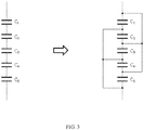
- FIG. 3 illustrates an equivalent circuit diagram of a capacitor 100 according to an embodiment of the present application.
- a laminated structure that a conductive layer and a dielectric layer are alternately stacked is adopted, and a plurality of columnar structures are provided, so that a larger capacitance value may be obtained under the condition of smaller device size, and thus capacitance density of the capacitor could be improved.
- the capacitor of the embodiment of the present application are described above, and a method for producing a capacitor of an embodiment of the present application will be described below.
- the method for producing the capacitor of the embodiment of the present application may prepare the capacitor of the foregoing embodiment of the present application, and the related descriptions in the following embodiment and the foregoing embodiments may be referred to each other.
- FIG. 4 illustrates a schematic flowchart of a method 400 for producing a capacitor according to an embodiment of the present application.
- a silicon wafer is selected as a substrate 510, and on a front surface of the substrate 510, photolithography is used, for example, photoresist is coated on the wafer first, then is exposed and developed, and a plurality of holes or trenches are processed by a deep reactive ion etching (Deep Reactive Ion Etching, DRIE) process.
- DRIE deep reactive ion etching
- the plurality of holes or trenches include a first hole or trench and a second hole or trench, and a size of the first hole or trench is greater than that of the second hole or trench.
- the plurality of holes or trenches include two sizes of holes or trenches with a large size and a small size.
- a depth-to-width ratio of the second hole or trench is greater than a predetermined threshold value.
- an opening width of the first hole or trench may be 20 microns and a depth thereof may be 100 microns
- an opening width of the second hole or trench may be 2 microns and a depth thereof may be 50 microns.
- the two sizes of holes or trenches may be manufactured at the same time or separately.
- an etching protection layer is produced on the first structure.
- a layer of silicon dioxide may be grown on the surface of holes or trenches by using a thermal oxidation process, as a corrosion protection layer 610 for subsequent removal of the substrate.
- the first laminated structure includes m dielectric layer(s) and m+1 conductive layers, the m dielectric layer(s) and the m+1 conductive layers form a structure that a conductive layer and a dielectric layer are adjacent to each other, and m is a positive integer.
- the first laminated structure may be formed by alternately depositing the conductive layers and the dielectric layers.
- the conductive layer may be deposited by atomic layer deposition (Atomic layer deposition, ALD), physical vapor deposition (Physical Vapor Deposition, PVD), chemical vapor deposition (Chemical Vapor Deposition, CVD), organometallic chemical vapor deposition, electroplating and other methods.
- ALD atomic layer deposition
- PVD Physical vapor deposition
- CVD chemical vapor deposition
- organometallic chemical vapor deposition organometallic chemical vapor deposition
- electroplating and other methods.
- the dielectric layer may be deposited by thermal oxidation, ALD, PVD, CVD and other methods.
- a layer of heavily doped polysilicon with a thickness of 200 nm is deposited on a surface of the corrosion protection layer 610 as a conductive layer 133; by using an ALD process, a layer of aluminum oxide with a thickness of 50 nm is deposited on a surface of the conductive layer 133 as a dielectric layer 138; by using an LPCVD process, a layer of heavily doped polysilicon with a thickness of 200 nm is deposited on a surface of the dielectric layer 138 as a conductive layer 132; by using an ALD process, a layer of aluminum oxide with a thickness of 50 nm is deposited on a surface of the conductive layer 132 as a dielectric layer 137; and by using an LPCVD process, a layer of heavily doped polysilicon with a thickness of 500 nm is deposited
- LPCVD Low Pressure Chemical Vapor Deposition
- a first insulating layer is produced on the first laminated structure to obtain a second structure.
- a thick layer of silicon dioxide may be deposited on the surface of the conductive layer 131 by using a CVD process, as a first insulating layer 161, so as to fill the large holes or trenches.
- a surface of the first insulating layer 161 may also be grinded flat.
- CMP Chemical Mechanical Polishing
- the second structure is turned over.
- the surface of the first insulating layer 161 may also be bonded to a carrier 910, and in FIG. 9 , a bonding layer 920 is between the first insulating layer 161 and the carrier 910.
- the surface of the first insulating layer 161 may be bonded to the carrier 910 by a bonding process, such as glass frit bonding (glass frit bonding).
- the substrate is removed to expose the first laminated structure.
- the substrate may be removed by wet etching or a combination of wet etching and dry etching.
- the substrate may be removed with a high concentration KOH solution at 80 degrees Celsius to expose the etching protection layer; then, the etching protection layer is removed by using a hydrofluoric acid solution to expose the conductive layer 133 of the first laminated structure, as shown in FIG. 10 .
- a second laminated structure is produced on the first laminated structure.
- the second laminated structure includes k dielectric layer(s) and k conductive layer(s), the k dielectric layer(s) and the k conductive layer(s) form a structure that a conductive layer and a dielectric layer are adjacent to each other and form, with the first laminated structure, a laminated structure that a conductive layer and a dielectric layer are adjacent to each other, the laminated structure forms a columnar structure at the hole or trench, and k is a positive integer.
- the production manner of the second laminated structure is similar to that of the first laminated structure.
- a layer of aluminum oxide with a thickness of 50 nm is deposited on the surface of the conductive layer 133 as a dielectric layer 139; by using an LPCVD process, a layer of heavily doped polysilicon with a thickness of 200 nm is deposited on a surface of the dielectric layer 139 as a conductive layer 134; by using an ALD process, a layer of aluminum oxide with a thickness of 50 nm is deposited on a surface of the conductive layer 134 as a dielectric layer 140; by using an LPCVD process, a layer of heavily doped polysilicon with a thickness of 200 nm is deposited on a surface of the dielectric layer 140 as a conductive layer 135; by using an ALD process, a layer of aluminum oxide with a thickness of 50 nm is deposited on a surface of the conductive layer 135 as a dielectric layer 141; and by using an LPCVD process,
- a second insulating layer is produced on the second laminated structure.
- a thick layer of silicon dioxide may be deposited on the surface of the conductive layer 136 by using a CVD process, as a second insulating layer 162.
- a surface of the second insulating layer 162 may also be grinded flat.
- the surface of the second insulating layer 162 may be grinded flat to obtain a structure as shown in FIG. 12 .
- the surface of the second insulating layer 162 is grinded flat until the conductive layer 136 at the uppermost of the second laminated structure is exposed. This may save subsequent etching steps and reduce cost.
- the first interconnection structure may be produced using the following manner.
- the second insulating layer 162 at the first hole or trench is etched to form a first step structure to expose the conductive layer to be connected.
- a step may be formed at a position above the first hole or trench to expose respective conductive layers.
- a first etching stop layer is deposited.
- a layer of silicon nitride may be deposited by using a CVD process as a first etching stop layer 1510.
- a third insulating layer 163 is deposited on the first etching stop layer 1510. Etching resistance of the first etching stop layer 1510 is greater than that of the third insulating layer 163. For example, by using a CVD process, a thick layer of silicon dioxide may be deposited on the first etching stop layer 1510, as the third insulating layer 163.
- the third insulating layer 163 is etched to obtain a hole that passes through the third insulating layer 163 until the first etching stop layer 1510 on the first step structure.
- through holes penetrating the third insulating layer 163 may be opened at positions corresponding to each step by a photolithography process. Since a material of the first etching stop layer 1510 is more resistant to etching than that of the third insulating layer 163, the bottom of each through hole is enabled to stay on the first etching stop layer 1510 of the corresponding step.
- the first etching stop layer in the hole is removed.
- the first etching stop layer exposed at the bottom of the hole may be removed by a dry or wet process.
- Metal is deposited in the hole to obtain a conductive through hole that passes through the third insulating layer 163 and the first etching stop layer 1510 and is connected to the specific conductive layer.
- a layer of titanium nitride may be deposited in the hole and filled with metallic tungsten.
- a first electrode and a second electrode are produced.
- the first electrode is electrically connected to an odd-numbered conductive layer among the m+k+1 conductive layers
- the second electrode is electrically connected to an even-numbered conductive layer among the m+k+1 conductive layers.
- a layer of metallic aluminum may be deposited by a PVD process, and a first electrode 110 and a second electrode 120 may be formed by photolithography, where the first electrode 110 communicates with the conductive layer 131, the conductive layer 133 and the conductive layer 135; and the second electrode 120 communicates with the conductive layer 132, the conductive layer 134 and the conductive layer 136.
- the carrier is thinned or the carrier and a bonding layer are removed.
- the thickness of the device is reduced through this step.
- the bonding layer and the carrier may be removed, and the capacitor shown in FIG. 1 may be obtained after removing the bonding layer and the carrier.
- the carrier may be thinned.
- the capacitor shown in FIG. 1 may be obtained by producing the first interconnection structure including the conductive through holes respectively connected to all conductive layers.
- the first electrode 110 is electrically connected to the odd-numbered conductive layer through the first interconnection structure
- the second electrode 120 is electrically connected to the even-numbered conductive layer through the first interconnection structure.
- the capacitor shown in FIG. 2 may be obtained by producing, on both sides of the laminated structure, the first interconnection structure and the second interconnection structure including the conductive through holes respectively connected to part of the conductive layers.
- the second interconnection structure may be produced after the first laminated structure is produced.
- the second interconnection structure may be produced using the following manner. It should be understood that, in addition to the following description, other details may refer to the production manner of the first interconnection structure.
- the first laminated structure is etched to form a second step structure to expose the conductive layer to be connected.
- a second etching stop layer 1520 is deposited.
- Etching resistance of the second etching stop layer 1520 is greater than that of the first insulating layer 161.
- the first insulating layer 161 is etched to obtain a hole that passes through the first insulating layer 161 until the second etching stop layer 1520 on the second step structure.
- the second etching stop layer in the hole is removed.
- Metal is deposited in the hole to obtain a conductive through hole that passes through the first insulating layer 161 and the second etching stop layer 1520 and is connected to the specific conductive layer, and metal interconnection among the conductive layers to be connected is formed.
- a fourth insulating layer 164 may also be produced on the second interconnection structure.
- both the first interconnection structure and the second interconnection structure include the conductive through holes respectively connected to part of the conductive layers; the first electrode 110 is electrically connected to the odd-numbered conductive layer through the first interconnection structure and the second interconnection structure, and the second electrode 120 is electrically connected to the even-numbered conductive layer through the first interconnection structure.
- a plurality of capacitors may be produced on one wafer, and then independent capacitors may be obtained by cutting.
- a laminated structure including a larger number of conductive layers and dielectric layers may be obtained by producing the laminated structure twice and a capacitance value of the capacitor is increased, and a plurality of holes or trenches are utilized to form a plurality of columnar structures of the laminated structure, which may further increase the capacitance value of the capacitor, thereby improving capacitance density of the capacitor.
Landscapes
- Engineering & Computer Science (AREA)
- Power Engineering (AREA)
- Microelectronics & Electronic Packaging (AREA)
- Manufacturing & Machinery (AREA)
- Semiconductor Integrated Circuits (AREA)
- Internal Circuitry In Semiconductor Integrated Circuit Devices (AREA)
Abstract
Description
- Embodiments of the present application relate to the field of capacitors, and more in particular, to a capacitor and a method for producing a capacitor.
- A capacitor is an important electronic component. With the continuous development of modern electronic system towards multi-function, high integration, low power consumption and miniaturization, an existing capacitor manufacturing technology has been unable to meet diversified needs of various high-end applications.
- A wafer-level three-dimensional (3D) capacitor is a new type of capacitor manufactured on a silicon wafer by utilizing a semiconductor processing technology in recent years. Compared with a commonly used multilayer ceramic capacitor, the wafer-level three-dimensional capacitor has significant advantages in terms of minimum thickness, frequency response, and temperature coefficient of a chip. The wafer-level 3D capacitor has a wide range of applications in consumer electronics that require an extremely small size of a device, or in medical, vehicle-mounted devices, aerospace electronics fields that require strict device performance and reliability.
- However, at present, capacitance density of the wafer-level 3D capacitor is still limited, and how to improve the capacitance density of the capacitor has become an urgent technical problem to be resolved.
- Embodiments of the present application provide a capacitor and a method for producing a capacitor, which could improve capacitance density of the capacitor.
- According to a first aspect, provided is a capacitor, including: an electrode layer including a first electrode and a second electrode separated from each other; a laminated structure including n dielectric layer(s) and n+1 conductive layers, where the n dielectric layer(s) and the n+1 conductive layers form a structure that a conductive layer and a dielectric layer are adjacent to each other, and the laminated structure forms at least two columnar structures, and n is a positive integer; and an interconnection structure configured to electrically connect an odd-numbered conductive layer in the n+1 conductive layers to the first electrode and electrically connect an even-numbered conductive layer in the n+1 conductive layers to the second electrode.
- According to the capacitor of the embodiments of the application, a laminated structure that a conductive layer and a dielectric layer are alternately stacked is adopted, and a plurality of columnar structures are provided, so that a larger capacitance value may be obtained under the condition of a smaller device size, and thus capacitance density of the capacitor could be improved.
- In some possible implementations, the at least two columnar structures include at least one first columnar structure and at least one second columnar structure, where a size of the first columnar structure is greater than that of the second columnar structure.
- In some possible implementations, the at least two columnar structures include one first columnar structure and at least two second columnar structures.
- By adopting a large-sized first columnar structure and a plurality of small-sized second columnar structures, it not only facilitates arrangement of an interconnection structure but also could improve the capacitance density to a great extent.
- In some possible implementations, a depth-to-width ratio of the second columnar structure is greater than a predetermined threshold value. For example, the predetermined threshold value may be 10; and the depth-to-width ratio of the second columnar structure may be 30.
- In some possible implementations, the interconnection structure is connected to the n+1 conductive layers at a top end of the first columnar structure.
- In some possible implementations, the interconnection structure is connected to the n+1 conductive layers at a top end of the first columnar structure and under the laminated structure. In this way, the interconnection structure provided at the first columnar structure may be reduced, so that the size of the first columnar structure may be reduced, and the capacity density may further be improved.
- In some possible implementations, the laminated structure is provided with a step structure, and the interconnection structure is connected to the n+1 conductive layers through the step structure.
- In some possible implementations, the columnar structure is a rectangular parallelepiped structure or a cylindrical structure.
- In some possible implementations, the capacitor further includes: an insulating layer disposed above and below the laminated structure.
- In some possible implementations, the interconnection structure is a conductive through hole that passes through the insulating layer and is respectively connected to the n+1 conductive layers.
- In some possible implementations, n is greater than or equal to 5.
- According to a second aspect, provided is a method for producing a capacitor, including: producing a plurality of holes or trenches on a substrate to obtain a first structure; producing a first laminated structure on the first structure, where the first laminated structure includes m dielectric layer(s) and m+1 conductive layers, the m dielectric layer(s) and the m+1 conductive layers form a structure that a conductive layer and a dielectric layer are adjacent to each other, and m is a positive integer; producing a first insulating layer on the first laminated structure to obtain a second structure; turning over the second structure; removing the substrate to expose the first laminated structure; producing a second laminated structure on the first laminated structure, where the second laminated structure includes k dielectric layer(s) and k conductive layer(s), the k dielectric layer(s) and the k conductive layer(s) form a structure that a conductive layer and a dielectric layer are adjacent to each other and form, with the first laminated structure, a laminated structure that a conductive layer and a dielectric layer are adjacent to each other, the laminated structure forms a columnar structure at the hole or trench, and k is a positive integer; producing a second insulating layer on the second laminated structure; and producing a first electrode and a second electrode, where the first electrode is electrically connected to an odd-numbered conductive layer among the m+k+1 conductive layers, and the second electrode is electrically connected to an even-numbered conductive layer among the m+k+1 conductive layers.
- According to the method for producing the capacitor provided by the embodiments of the present invention, a laminated structure including a larger number of conductive layers and dielectric layers may be obtained by producing the laminated structure twice and a capacitance value of the capacitor is increased, and a plurality of holes or trenches are utilized to form a plurality of columnar structures of the laminated structure, which may further increase the capacitance value of the capacitor, thereby improving capacitance density of the capacitor.
- In some possible implementations, the plurality of holes or trenches include a first hole or trench and a second hole or trench, and a size of the first hole or trench is greater than that of the second hole or trench.
- In some possible implementations, a depth-to-width ratio of the second hole or trench is greater than a predetermined threshold value.
- In some possible implementations, before the producing the first laminated structure on the first structure, the method further includes: producing an etching protection layer on the first structure; where the removing the substrate to expose the first laminated structure includes: removing the substrate to expose the etching protection layer, and then removing the etching protection layer to expose the first laminated structure.
- In some possible implementations, before the turning over the second structure, the method further includes: grinding a surface of the first insulating layer flat.
- In some possible implementations, after the turning over the second structure, the method further includes: bonding the surface of the first insulating layer to a carrier.
- In some possible implementations, after the producing the first electrode and the second electrode, the method further includes: thinning the carrier or removing the carrier and a bonding layer.
- In some possible implementations, after the producing the second insulating layer on the second laminated structure, the method further includes: grinding a surface of the second insulating layer flat.
- In some possible implementations, the surface of the second insulating layer is grinded flat until the conductive layer at the uppermost of the second laminated structure is exposed.
- In some possible implementations, before the producing the first electrode and the second electrode, the method further includes: producing a first interconnection structure, where the first interconnection structure includes a conductive through hole respectively connected to all or part of the conductive layers.
- In some possible implementations, when the first interconnection structure includes the conductive through hole respectively connected to the all conductive layers, the first electrode is electrically connected to the odd-numbered conductive layer through the first interconnection structure, and the second electrode is electrically connected to the even-numbered conductive layer through the first interconnection structure.
- In some possible implementations, when the first interconnection structure includes the conductive through hole respectively connected to the part of the conductive layers, the method further includes: producing a second interconnection structure after the producing the first laminated structure on the first structure; where the first electrode is electrically connected to the odd-numbered conductive layer through the first interconnection structure and the second interconnection structure, and the second electrode is electrically connected to the even-numbered conductive layer through the first interconnection structure.
- In some possible implementations, the producing the first interconnection structure includes: etching the second insulating layer at the first hole or trench to form a first step structure to expose the conductive layer to be connected; depositing a first etching stop layer; depositing a third insulating layer on the first etching stop layer, where etching resistance of the first etching stop layer is greater than that of the third insulating layer; for a specific conductive layer, etching the third insulating layer to obtain a hole that passes through the third insulating layer until the first etching stop layer on the first step structure; removing the first etching stop layer in the hole; and depositing metal in the hole to obtain a conductive through hole that passes through the third insulating layer and the first etching stop layer and is connected to the specific conductive layer.
- In some possible implementations, the producing the second interconnection structure includes: before the producing the first insulating layer on the first laminated structure, etching the first laminated structure to form a second step structure to expose the conductive layer to be connected; depositing a second etching stop layer, where etching resistance of the second etching stop layer is greater than that of the first insulating layer; after the producing the first insulating layer on the first laminated structure, for a specific conductive layer, etching the first insulating layer to obtain a hole that passes through the first insulating layer until the second etching stop layer on the second step structure; removing the second etching stop layer in the hole; and depositing metal in the hole to obtain a conductive through hole that passes through the first insulating layer and the second etching stop layer and is connected to the specific conductive layer, and forming metal interconnection among the conductive layers to be connected.
- In some possible implementations, after the producing the second interconnection structure, the method further includes: producing a fourth insulating layer on the second interconnection structure.
- In some possible implementations, the method further includes: obtaining independent capacitors by cutting.
-
-
FIG. 1 is a schematic diagram of a capacitor according to an embodiment of the present application. -
FIG. 2 is a schematic diagram of a capacitor according to another embodiment of the present application. -
FIG. 3 is an equivalent circuit diagram of a capacitor according to an embodiment of the present application. -
FIG. 4 is a schematic flowchart of a method for producing a capacitor according to an embodiment of the present application. -
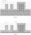
FIGS. 5-17 are schematic diagrams of production processes of a capacitor according to an embodiment of the present application. - Technical solutions in embodiments of the present application will be described hereinafter with reference to the accompanying drawings.
-
FIG. 1 illustrates a schematic diagram of acapacitor 100 according to an embodiment of the present application. - The
capacitor 100 is a wafer-level 3D capacitor, andFIG. 1 is a cross-sectional view thereof. - As shown in
FIG. 1 , thecapacitor 100 may include afirst electrode 110, asecond electrode 120, a laminatedstructure 130 and aninterconnection structure 150. - The
first electrode 110 and thesecond electrode 120 are positive and negative electrodes of thecapacitor 100. Thefirst electrode 110 and thesecond electrode 120 are separated from each other to form an electrode layer. The materials of thefirst electrode 110 and thesecond electrode 120 may adopt various conductive materials, such as metallic aluminum. - The laminated
structure 130 includes n dielectric layer(s) and n+1 conductive layers, and n is a positive integer. Optionally, in one embodiment, n is 5, that is, the laminatedstructure 130 may include six conductive layers such as conductive layers 131-136 shown inFIG. 1 , and five dielectric layers such as dielectric layers 137-141 shown inFIG. 1 . - As shown in
FIG. 1 , the n dielectric layers and the n+1 conductive layers form a structure that a conductive layer and a dielectric layer are adjacent to each other, that is, the laminatedstructure 130 is a laminated structure that a conductive layer and a dielectric layer are alternately stacked. Since there is one more layer of the conductive layer, the uppermost layer and the lowermost layer of the laminatedstructure 130 are conductive layers. - In addition, the laminated
structure 130 forms at least two columnar structures, such as a firstcolumnar structure 145 and a secondcolumnar structure 146 as shown inFIG. 1 . - Optionally, the columnar structure may be a rectangular parallelepiped structure (including a wall structure) or a cylindrical structure.
- The existence of the columnar structure is equivalent to increasing a plate area of the capacitor, so it is beneficial to improve the capacitance value of the capacitor.
- Optionally, a material of the dielectric layer in the laminated
structure 130 may be silicon oxide, silicon nitride, metal oxide, metal nitride, etc., such as silicon dioxide, silicon nitride, or high dielectric constant materials including aluminum oxide, hafnium oxide, zirconium oxide, titanium dioxide, Y2O3, La2O3, HfSiO4, LaAlO3, SrTiO3, LaLuO3, etc. It may also be one or a combination of the foregoing materials. - Optionally, a material of the conductive layer in the
laminated structure 130 may be heavily doped polysilicon, carbon material, or various metals such as aluminum, tungsten, copper, titanium, tantalum, etc., or compounds with low resistivity such as titanium nitride and tantalum nitride, or a laminated layer or combination of the foregoing conductive materials. - The interconnection structure is configured to electrically connect an odd-numbered conductive layer in the n+1 conductive layers to the
first electrode 110 and electrically connect an even-numbered conductive layer in the n+1 conductive layers to thesecond electrode 120. - It should be understood that in the embodiment of the present application, the order of the conductive layers involved may be from one side to the other side of the
laminated structure 140, for example, from top to bottom or from bottom to top. For convenience of description, the following description will take the order from bottom to top as an example. For example, inFIG. 1 , the conductive layers 131-136 are the first to the sixth conductive layers, respectively. - As shown in
FIG. 1 , odd-numbered conductive layers among the conductive layers 131-136, that is, the first, third and fifth conductive layers, are electrically connected to thefirst electrode 110 through theinterconnection structure 150, and even-numbered conductive layers among the conductive layers 131-136, that is, the second, fourth and sixth conductive layers, are electrically connected to thesecond electrode 120 through theinterconnection structure 150. - A material of the
interconnection structure 150 may adopt various conductive materials, which may be the same as or different from the material of the conductive layer in thelaminated structure 130, for example, titanium nitride and metallic tungsten may be adopted. - Optionally, in an embodiment of the present application, the at least two columnar structures include at least one first
columnar structure 145 and at least one secondcolumnar structure 146, where a size of the firstcolumnar structure 145 is greater than that of the secondcolumnar structure 146. In other words, for thecapacitor 100, it includes two sizes of columnar structures. - In the embodiment of the present application, the size of the columnar structure may be a width of the columnar structure, that is, the width in the lateral direction in
FIG. 1 . - For example, the size of the first
columnar structure 145 may be 20 microns, and the size of the secondcolumnar structure 146 may be 2 microns, but the embodiment of the present application is not limited thereto. - Optionally, in an embodiment of the present application, as shown in
FIG. 1 , the at least two columnar structures include one firstcolumnar structure 145 and at least two secondcolumnar structures 146. - Optionally, a depth-to-width ratio of the second
columnar structure 146 is greater than a predetermined threshold value. For example, the predetermined threshold value may be 10; and the depth-to-width ratio of the second columnar structure may be 30. - From the perspective of improving the capacitance density, the use of a larger number of small-sized columnar structures with large depth-width ratios could maximize the capacitance density. However, the small-sized columnar structure is not convenient to provide the
interconnection structure 150, and therefore a large-sized columnar structure may be used to provide theinterconnection structure 150. In other words, by adopting a large-sized firstcolumnar structure 145 and a plurality of small-sized secondcolumnar structures 146, it not only facilitates arrangement of aninterconnection structure 150, but also could improve the capacitance density to a great extent. - Optionally, in an embodiment of the present application, as shown in
FIG. 1 , theinterconnection structure 150 is connected to the n+1 conductive layers at a top end of the firstcolumnar structure 145. - Optionally, in an embodiment of the present application, as shown in
FIG. 2 , theinterconnection structure 150 is connected to the n+1 conductive layers at a top end of the firstcolumnar structure 145 and under thelaminated structure 130. - In the foregoing embodiment, the
interconnection structure 150 is only provided at the position of the firstcolumnar structure 145. In this embodiment, part of theinterconnection structure 150 may be dispersedly provided below thelaminated structure 130. It is easy to implement that some interconnection structures are dispersedly provided below thelaminated structure 130, which may reduce the interconnection structure provided at the firstcolumnar structure 145, thereby reducing the size of the firstcolumnar structure 145, and further improving the capacitance density. - It should be understood that, except for the different settings of the
interconnection structure 150, the other settings inFIG. 2 and FIG. 1 are the same, details are not described herein for brevity. - As shown in
FIGS. 1 and 2 , thelaminated structure 130 is provided with a step structure, and theinterconnection structure 150 is connected to the n+1 conductive layers through the step structure. The arrangement of the step structure facilitates the connection and isolation between different conductive layers. - Optionally, in an embodiment of the present application, as shown in
FIGS. 1 and 2 , thecapacitor 100 may further include:
an insulatinglayer 160 disposed above and below thelaminated structure 130. - It should be understood that to be above and below the laminated structure are relative to the whole laminated structure, that is, to be above the laminated structure means to be above a top layer of the laminated structure, and to be below the laminated structure means to be below a bottom layer of the laminated structure.
- In this case, the
interconnection structure 150 is a conductive through hole that passes through the insulatinglayer 160 and is respectively connected to the n+1 conductive layers. - As shown in
FIGS. 1 and 2 , the electrical connection of thefirst electrode 110 and thesecond electrode 120 to the corresponding conductive layers may be realized by providing the conductive through hole in the insulatinglayer 160. - Optionally, a material of the insulating
layer 160 may be an organic polymer material, including polyimide (Polyimide), parylene (Parylene), benzocyclobutene (BCB), etc., it may also be some inorganic materials, including spin on glass (Spin on glass, SOG), undoped silicon glass (Undoped Silicon Glass, USG), silicon oxide synthesized by tetraethyl orthosilicate (Tetraethyl Orthosilicate, TEOS), silicon oxide, silicon nitride and ceramic; and it may also be a combination of the foregoing materials. -
FIG. 3 illustrates an equivalent circuit diagram of acapacitor 100 according to an embodiment of the present application. - Taking n being 5 as an example, as shown in
FIG. 3 , six conductive layers and five dielectric layers that are alternately stacked are equivalent to five capacitors connected in series with each other (each dielectric layer corresponds to one capacitor). After theinterconnection structure 150 of the embodiment of the present application is adopted, the five capacitors are connected in parallel to obtain thecapacitor 100 of the embodiment of the present application. Therefore, thecapacitor 100 of the embodiment of the present application has a larger capacitance value. - According to the capacitor of the embodiments of the application, a laminated structure that a conductive layer and a dielectric layer are alternately stacked is adopted, and a plurality of columnar structures are provided, so that a larger capacitance value may be obtained under the condition of smaller device size, and thus capacitance density of the capacitor could be improved.
- The capacitor of the embodiment of the present application are described above, and a method for producing a capacitor of an embodiment of the present application will be described below. The method for producing the capacitor of the embodiment of the present application may prepare the capacitor of the foregoing embodiment of the present application, and the related descriptions in the following embodiment and the foregoing embodiments may be referred to each other.
-
FIG. 4 illustrates a schematic flowchart of amethod 400 for producing a capacitor according to an embodiment of the present application. - 401, a plurality of holes or trenches are produced on a substrate to obtain a first structure.
- As shown in
FIG. 5 , a silicon wafer is selected as asubstrate 510, and on a front surface of thesubstrate 510, photolithography is used, for example, photoresist is coated on the wafer first, then is exposed and developed, and a plurality of holes or trenches are processed by a deep reactive ion etching (Deep Reactive Ion Etching, DRIE) process. - Optionally, the plurality of holes or trenches include a first hole or trench and a second hole or trench, and a size of the first hole or trench is greater than that of the second hole or trench. In other words, the plurality of holes or trenches include two sizes of holes or trenches with a large size and a small size.
- Optionally, a depth-to-width ratio of the second hole or trench is greater than a predetermined threshold value.
- As an example, an opening width of the first hole or trench may be 20 microns and a depth thereof may be 100 microns, and an opening width of the second hole or trench may be 2 microns and a depth thereof may be 50 microns.
- The two sizes of holes or trenches may be manufactured at the same time or separately.
- 402, an etching protection layer is produced on the first structure.
- For example, as shown in
FIG. 6 , a layer of silicon dioxide may be grown on the surface of holes or trenches by using a thermal oxidation process, as acorrosion protection layer 610 for subsequent removal of the substrate. - 403, a first laminated structure is produced on the first structure.
- The first laminated structure includes m dielectric layer(s) and m+1 conductive layers, the m dielectric layer(s) and the m+1 conductive layers form a structure that a conductive layer and a dielectric layer are adjacent to each other, and m is a positive integer.
- The first laminated structure may be formed by alternately depositing the conductive layers and the dielectric layers.
- The conductive layer may be deposited by atomic layer deposition (Atomic layer deposition, ALD), physical vapor deposition (Physical Vapor Deposition, PVD), chemical vapor deposition (Chemical Vapor Deposition, CVD), organometallic chemical vapor deposition, electroplating and other methods. The dielectric layer may be deposited by thermal oxidation, ALD, PVD, CVD and other methods.
- For example, as shown in
FIG. 7 , by using a low pressure chemical vapor deposition (Low Pressure Chemical Vapor Deposition, LPCVD) process, a layer of heavily doped polysilicon with a thickness of 200 nm is deposited on a surface of thecorrosion protection layer 610 as aconductive layer 133; by using an ALD process, a layer of aluminum oxide with a thickness of 50 nm is deposited on a surface of theconductive layer 133 as adielectric layer 138; by using an LPCVD process, a layer of heavily doped polysilicon with a thickness of 200 nm is deposited on a surface of thedielectric layer 138 as aconductive layer 132; by using an ALD process, a layer of aluminum oxide with a thickness of 50 nm is deposited on a surface of theconductive layer 132 as adielectric layer 137; and by using an LPCVD process, a layer of heavily doped polysilicon with a thickness of 500 nm is deposited on a surface of thedielectric layer 137 as aconductive layer 131. Finally, a structure shown inFIG. 7 is obtained. Optionally, small holes or trenches may be filled, while large holes or trenches may not be filled. - 404, a first insulating layer is produced on the first laminated structure to obtain a second structure.
- For example, as shown in
FIG. 8 , a thick layer of silicon dioxide may be deposited on the surface of theconductive layer 131 by using a CVD process, as a first insulatinglayer 161, so as to fill the large holes or trenches. - Optionally, a surface of the first insulating
layer 161 may also be grinded flat. For example, by using a chemical mechanical polishing (Chemical Mechanical Polishing, CMP) process, the surface of the first insulatinglayer 161 may be grinded flat to obtain a second structure as shown inFIG. 8 . - 405, the second structure is turned over.
- Optionally, as shown in
FIG. 9 , the surface of the first insulatinglayer 161 may also be bonded to acarrier 910, and inFIG. 9 , abonding layer 920 is between the first insulatinglayer 161 and thecarrier 910. - For example, the surface of the first insulating
layer 161 may be bonded to thecarrier 910 by a bonding process, such as glass frit bonding (glass frit bonding). - 406, the substrate is removed to expose the first laminated structure.
- The substrate may be removed by wet etching or a combination of wet etching and dry etching.
- For example, the substrate may be removed with a high concentration KOH solution at 80 degrees Celsius to expose the etching protection layer; then, the etching protection layer is removed by using a hydrofluoric acid solution to expose the
conductive layer 133 of the first laminated structure, as shown inFIG. 10 . - 407, a second laminated structure is produced on the first laminated structure.
- The second laminated structure includes k dielectric layer(s) and k conductive layer(s), the k dielectric layer(s) and the k conductive layer(s) form a structure that a conductive layer and a dielectric layer are adjacent to each other and form, with the first laminated structure, a laminated structure that a conductive layer and a dielectric layer are adjacent to each other, the laminated structure forms a columnar structure at the hole or trench, and k is a positive integer.
- The production manner of the second laminated structure is similar to that of the first laminated structure.
- For example, as shown in
FIG. 11 , by using an ALD process, a layer of aluminum oxide with a thickness of 50 nm is deposited on the surface of theconductive layer 133 as adielectric layer 139; by using an LPCVD process, a layer of heavily doped polysilicon with a thickness of 200 nm is deposited on a surface of thedielectric layer 139 as aconductive layer 134; by using an ALD process, a layer of aluminum oxide with a thickness of 50 nm is deposited on a surface of theconductive layer 134 as adielectric layer 140; by using an LPCVD process, a layer of heavily doped polysilicon with a thickness of 200 nm is deposited on a surface of thedielectric layer 140 as aconductive layer 135; by using an ALD process, a layer of aluminum oxide with a thickness of 50 nm is deposited on a surface of theconductive layer 135 as adielectric layer 141; and by using an LPCVD process, a layer of heavily doped polysilicon with a thickness of 200 nm is deposited on a surface of thedielectric layer 141 as aconductive layer 136. Finally, a structure shown inFIG. 11 is obtained. - 408, a second insulating layer is produced on the second laminated structure.
- For example, as shown in
FIG. 12 , a thick layer of silicon dioxide may be deposited on the surface of theconductive layer 136 by using a CVD process, as a second insulatinglayer 162. - Optionally, a surface of the second insulating
layer 162 may also be grinded flat. For example, by using a CMP process, the surface of the second insulatinglayer 162 may be grinded flat to obtain a structure as shown inFIG. 12 . - Optionally, as another embodiment, as shown in
FIG. 13 , the surface of the second insulatinglayer 162 is grinded flat until theconductive layer 136 at the uppermost of the second laminated structure is exposed. This may save subsequent etching steps and reduce cost. - 409, a first interconnection structure is produced.
- Optionally, the first interconnection structure may be produced using the following manner.
- The second
insulating layer 162 at the first hole or trench is etched to form a first step structure to expose the conductive layer to be connected. For example, as shown inFIG. 14 , by using multiple steps of a photolithography process, a step may be formed at a position above the first hole or trench to expose respective conductive layers. - A first etching stop layer is deposited. For example, as shown in
FIG. 15 , a layer of silicon nitride may be deposited by using a CVD process as a firstetching stop layer 1510. - A third insulating
layer 163 is deposited on the firstetching stop layer 1510. Etching resistance of the firstetching stop layer 1510 is greater than that of the third insulatinglayer 163. For example, by using a CVD process, a thick layer of silicon dioxide may be deposited on the firstetching stop layer 1510, as the third insulatinglayer 163. - For a specific conductive layer, the third insulating
layer 163 is etched to obtain a hole that passes through the third insulatinglayer 163 until the firstetching stop layer 1510 on the first step structure. For example, through holes penetrating the third insulatinglayer 163 may be opened at positions corresponding to each step by a photolithography process. Since a material of the firstetching stop layer 1510 is more resistant to etching than that of the third insulatinglayer 163, the bottom of each through hole is enabled to stay on the firstetching stop layer 1510 of the corresponding step. - The first etching stop layer in the hole is removed. For example, the first etching stop layer exposed at the bottom of the hole may be removed by a dry or wet process.
- Metal is deposited in the hole to obtain a conductive through hole that passes through the third insulating
layer 163 and the firstetching stop layer 1510 and is connected to the specific conductive layer. For example, a layer of titanium nitride may be deposited in the hole and filled with metallic tungsten. Finally, the redundant conductive materials and insulating materials on the surface are removed by a planarization process, and a structure shown inFIG. 16 is obtained. - 410, a first electrode and a second electrode are produced.
- The first electrode is electrically connected to an odd-numbered conductive layer among the m+k+1 conductive layers, and the second electrode is electrically connected to an even-numbered conductive layer among the m+k+1 conductive layers.
- For example, as shown in
FIG. 17 , a layer of metallic aluminum may be deposited by a PVD process, and afirst electrode 110 and asecond electrode 120 may be formed by photolithography, where thefirst electrode 110 communicates with theconductive layer 131, theconductive layer 133 and theconductive layer 135; and thesecond electrode 120 communicates with theconductive layer 132, theconductive layer 134 and theconductive layer 136. - 411, the carrier is thinned or the carrier and a bonding layer are removed.
- The thickness of the device is reduced through this step. In one implementation, the bonding layer and the carrier may be removed, and the capacitor shown in
FIG. 1 may be obtained after removing the bonding layer and the carrier. In another implementation, when the carrier and the bonding layer cannot be removed, the carrier may be thinned. - In the foregoing embodiments, the capacitor shown in
FIG. 1 may be obtained by producing the first interconnection structure including the conductive through holes respectively connected to all conductive layers. In this case, thefirst electrode 110 is electrically connected to the odd-numbered conductive layer through the first interconnection structure, and thesecond electrode 120 is electrically connected to the even-numbered conductive layer through the first interconnection structure. - Optionally, the capacitor shown in
FIG. 2 may be obtained by producing, on both sides of the laminated structure, the first interconnection structure and the second interconnection structure including the conductive through holes respectively connected to part of the conductive layers. - Specifically, the second interconnection structure may be produced after the first laminated structure is produced.
- Optionally, the second interconnection structure may be produced using the following manner. It should be understood that, in addition to the following description, other details may refer to the production manner of the first interconnection structure.
- Before producing the first insulating
layer 161, the first laminated structure is etched to form a second step structure to expose the conductive layer to be connected. - A second
etching stop layer 1520 is deposited. - Etching resistance of the second
etching stop layer 1520 is greater than that of the first insulatinglayer 161. - After producing the first insulating
layer 161, for a specific conductive layer, the first insulatinglayer 161 is etched to obtain a hole that passes through the first insulatinglayer 161 until the secondetching stop layer 1520 on the second step structure. - The second etching stop layer in the hole is removed.
- Metal is deposited in the hole to obtain a conductive through hole that passes through the first insulating
layer 161 and the secondetching stop layer 1520 and is connected to the specific conductive layer, and metal interconnection among the conductive layers to be connected is formed. - Optionally, after producing the second interconnect structure, a fourth insulating
layer 164 may also be produced on the second interconnection structure. - In this embodiment, both the first interconnection structure and the second interconnection structure include the conductive through holes respectively connected to part of the conductive layers; the
first electrode 110 is electrically connected to the odd-numbered conductive layer through the first interconnection structure and the second interconnection structure, and thesecond electrode 120 is electrically connected to the even-numbered conductive layer through the first interconnection structure. - In this way, a plurality of capacitors may be produced on one wafer, and then independent capacitors may be obtained by cutting.
- According to the method for producing the capacitor provided by the embodiments of the present invention, a laminated structure including a larger number of conductive layers and dielectric layers may be obtained by producing the laminated structure twice and a capacitance value of the capacitor is increased, and a plurality of holes or trenches are utilized to form a plurality of columnar structures of the laminated structure, which may further increase the capacitance value of the capacitor, thereby improving capacitance density of the capacitor.
- It should be noted that specific examples in embodiments of the present application are just intended to help a person skilled in the art better understand the embodiments of the present application, rather than for limiting the scope of the present application.
- It should also be noted that terms used in embodiments of the present application and the claims appended hereto are merely for the purpose of describing particular embodiments, and are not intended to limit the embodiments of the present application. For example, the use of a singular form of "a", "the" and "said" in the embodiment of the present application and the claims appended hereto are also intended to include a plural form, unless otherwise clearly indicated herein by context.
- The foregoing description is only a specific implementation manner of the present application. The protection scope of the present application, however, is not limited here. Various modifications or replacements may be readily conceivable to any person skilled in the art within the technical scope disclosed in the present application, and such modifications or replacements shall fall within the protection scope of the present application. Therefore, the protection scope of this application shall be subject to the protection scope of the claims.
Claims (27)
- A capacitor, comprising:an electrode layer comprising a first electrode and a second electrode separated from each other;a laminated structure comprising n dielectric layer(s) and n+1 conductive layers, wherein the n dielectric layer(s) and the n+1 conductive layers form a structure that a conductive layer and a dielectric layer are adjacent to each other, and the laminated structure forms at least two columnar structures, and n is a positive integer; andan interconnection structure configured to electrically connect an odd-numbered conductive layer in the n+1 conductive layers to the first electrode and electrically connect an even-numbered conductive layer in the n+1 conductive layers to the second electrode.
- The capacitor according to claim 1, wherein the at least two columnar structures comprise at least one first columnar structure and at least one second columnar structure, wherein a size of the first columnar structure is greater than that of the second columnar structure.
- The capacitor according to claim 2, wherein the at least two columnar structures comprise one first columnar structure and at least two second columnar structures.
- The capacitor according to claim 2 or 3, wherein a depth-to-width ratio of the second columnar structure is greater than a predetermined threshold value.
- The capacitor according to any one of claims 2 to 4, wherein the interconnection structure is connected to the n+1 conductive layers at a top end of the first columnar structure.
- The capacitor according to any one of claims 2 to 4, wherein the interconnection structure is connected to the n+1 conductive layers at a top end of the first columnar structure and under the laminated structure.
- The capacitor according to any one of claims 1 to 6, wherein the laminated structure is provided with a step structure, and the interconnection structure is connected to the n+1 conductive layers through the step structure.
- The capacitor according to any one of claims 1 to 7, wherein the columnar structure is a rectangular parallelepiped structure or a cylindrical structure.
- The capacitor according to any one of claims 1 to 8, wherein the capacitor further comprises:
an insulating layer disposed above and below the laminated structure. - The capacitor according to claim 9, wherein the interconnection structure is a conductive through hole that passes through the insulating layer and is respectively connected to the n+1 conductive layers.
- The capacitor according to any one of claims 1 to 9, wherein n is greater than or equal to 5.
- A method for producing a capacitor, comprising:producing a plurality of holes or trenches on a substrate to obtain a first structure;producing a first laminated structure on the first structure, wherein the first laminated structure comprises m dielectric layer(s) and m+1 conductive layers, the m dielectric layer(s) and the m+1 conductive layers form a structure that a conductive layer and a dielectric layer are adjacent to each other, and m is a positive integer;producing a first insulating layer on the first laminated structure to obtain a second structure;turning over the second structure;removing the substrate to expose the first laminated structure;producing a second laminated structure on the first laminated structure, wherein the second laminated structure comprises k dielectric layer(s) and k conductive layer(s), the k dielectric layer(s) and the k conductive layer(s) form a structure that a conductive layer and a dielectric layer are adjacent to each other and form, with the first laminated structure, a laminated structure that a conductive layer and a dielectric layer are adjacent to each other, the laminated structure forms a columnar structure at the hole or trench, and k is a positive integer;producing a second insulating layer on the second laminated structure; andproducing a first electrode and a second electrode, wherein the first electrode is electrically connected to an odd-numbered conductive layer among the m+k+1 conductive layers, and the second electrode is electrically connected to an even-numbered conductive layer among the m+k+1 conductive layers.
- The method according to claim 12, wherein the plurality of holes or trenches comprise a first hole or trench and a second hole or trench, and a size of the first hole or trench is greater than that of the second hole or trench.
- The method according to claim 13, wherein a depth-to-width ratio of the second hole or trench is greater than a predetermined threshold value.
- The method according to any one of claims 12 to 14, wherein before the producing the first laminated structure on the first structure, the method further comprises:producing an etching protection layer on the first structure;wherein the removing the substrate to expose the first laminated structure comprises:
removing the substrate to expose the etching protection layer, and then removing the etching protection layer to expose the first laminated structure. - The method according to any one of claims 12to 15, wherein before the turning over the second structure, the method further comprises:
grinding a surface of the first insulating layer flat. - The method according to claim 16, wherein after the turning over the second structure, the method further comprises:
bonding the surface of the first insulating layer to a carrier. - The method according to claim 17, wherein after the producing the first electrode and the second electrode, the method further comprises:
thinning the carrier or removing the carrier and a bonding layer. - The method according to any one of claims 12 to 18, wherein after the producing the second insulating layer on the second laminated structure, the method further comprises:
grinding a surface of the second insulating layer flat. - The method according to claim 19, wherein the surface of the second insulating layer is grinded flat until the conductive layer at the uppermost of the second laminated structure is exposed.
- The method according to any one of claims 12 to 20, wherein before the producing the first electrode and the second electrode, the method further comprises:
producing a first interconnection structure, wherein the first interconnection structure comprises a conductive through hole respectively connected to all or part of the conductive layers. - The method according to claim 21, wherein when the first interconnection structure comprises the conductive through hole respectively connected to the all conductive layers, the first electrode is electrically connected to the odd-numbered conductive layer through the first interconnection structure, and the second electrode is electrically connected to the even-numbered conductive layer through the first interconnection structure.
- The method according to claim 21, wherein when the first interconnection structure comprises the conductive through hole respectively connected to the part of the conductive layers, the method further comprises:producing a second interconnection structure after the producing the first laminated structure on the first structure;wherein the first electrode is electrically connected to the odd-numbered conductive layer through the first interconnection structure and the second interconnection structure, and the second electrode is electrically connected to the even-numbered conductive layer through the first interconnection structure.
- The method according to any one of claims 21 to 23, wherein the producing the first interconnection structure comprises:etching the second insulating layer at the first hole or trench to form a first step structure to expose the conductive layer to be connected;depositing a first etching stop layer;depositing a third insulating layer on the first etching stop layer, wherein etching resistance of the first etching stop layer is greater than that of the third insulating layer;for a specific conductive layer, etching the third insulating layer to obtain a hole that passes through the third insulating layer until the first etching stop layer on the first step structure;removing the first etching stop layer in the hole; anddepositing metal in the hole to obtain a conductive through hole that passes through the third insulating layer and the first etching stop layer and is connected to the specific conductive layer.
- The method according to claim 23, wherein the producing the second interconnection structure comprises:before the producing the first insulating layer on the first laminated structure, etching the first laminated structure to form a second step structure to expose the conductive layer to be connected;depositing a second etching stop layer, wherein etching resistance of the second etching stop layer is greater than that of the first insulating layer;after the producing the first insulating layer on the first laminated structure, for a specific conductive layer, etching the first insulating layer to obtain a hole that passes through the first insulating layer until the second etching stop layer on the second step structure;removing the second etching stop layer in the hole; anddepositing metal in the hole to obtain a conductive through hole that passes through the first insulating layer and the second etching stop layer and is connected to the specific conductive layer, and forming metal interconnection among the conductive layers to be connected.
- The method according to claim 23 or 25, wherein after the producing the second interconnection structure, the method further comprises:
producing a fourth insulating layer on the second interconnection structure. - The method according to any one of claims 12 to 26, wherein the method further comprises:
obtaining independent capacitors by cutting.
Applications Claiming Priority (1)
| Application Number | Priority Date | Filing Date | Title |
|---|---|---|---|
| PCT/CN2018/123575 WO2020132884A1 (en) | 2018-12-25 | 2018-12-25 | Capacitor and method for preparing capacitor |
Publications (2)
| Publication Number | Publication Date |
|---|---|
| EP3754725A1 true EP3754725A1 (en) | 2020-12-23 |
| EP3754725A4 EP3754725A4 (en) | 2021-05-12 |
Family
ID=71127300
Family Applications (1)
| Application Number | Title | Priority Date | Filing Date |
|---|---|---|---|
| EP18944231.2A Withdrawn EP3754725A4 (en) | 2018-12-25 | 2018-12-25 | CAPACITOR AND CONDENSER PREPARATION PROCESS |
Country Status (4)
| Country | Link |
|---|---|
| US (1) | US11239308B2 (en) |
| EP (1) | EP3754725A4 (en) |
| CN (1) | CN111615751B (en) |
| WO (1) | WO2020132884A1 (en) |
Cited By (1)
| Publication number | Priority date | Publication date | Assignee | Title |
|---|---|---|---|---|
| EP4184537A1 (en) * | 2021-11-18 | 2023-05-24 | Murata Manufacturing Co., Ltd. | An electrical device comprising stacked capacitive structures with electrodes connected from bottom to top and top to bottom |
Families Citing this family (3)
| Publication number | Priority date | Publication date | Assignee | Title |
|---|---|---|---|---|
| US20240055345A1 (en) * | 2022-08-11 | 2024-02-15 | Intel Corporation | Alternating high k layers on glass pillars for super capacitors on glass substrates |
| US20240304662A1 (en) * | 2023-03-08 | 2024-09-12 | Taiwan Semiconductor Manufacturing Company, Ltd. | Capacitor having conducitve pillar structures configured to increase capacitance density |
| KR102749937B1 (en) * | 2023-11-28 | 2025-01-03 | 엘스페스 주식회사 | Compound capacitor and manufacturing method thereof |
Family Cites Families (16)
| Publication number | Priority date | Publication date | Assignee | Title |
|---|---|---|---|---|
| KR920004028B1 (en) * | 1989-11-20 | 1992-05-22 | 삼성전자 주식회사 | Semiconductor device and manufacturing method thereof |
| US7190016B2 (en) * | 2004-10-08 | 2007-03-13 | Rohm And Haas Electronic Materials Llc | Capacitor structure |
| US8085524B2 (en) | 2005-11-08 | 2011-12-27 | Ipdia | Integrated capacitor arrangement for ultrahigh capacitance values |
| SE534510C2 (en) * | 2008-11-19 | 2011-09-13 | Silex Microsystems Ab | Functional encapsulation |
| CN102339671A (en) * | 2010-07-21 | 2012-02-01 | 马长兆 | Plane laminated solid capacitor |
| US8405135B2 (en) | 2010-10-05 | 2013-03-26 | International Business Machines Corporation | 3D via capacitor with a floating conductive plate for improved reliability |
| US8962423B2 (en) * | 2012-01-18 | 2015-02-24 | International Business Machines Corporation | Multilayer MIM capacitor |
| FR2993397A1 (en) * | 2012-07-16 | 2014-01-17 | St Microelectronics Sa | SEMICONDUCTOR DEVICE COMPRISING AN INTEGRATED CAPACITOR AND METHOD OF MANUFACTURING |
| US9978829B2 (en) * | 2012-11-26 | 2018-05-22 | Taiwan Semiconductor Manufacturing Co., Ltd. | Low impedance high density deep trench capacitor |
| FR3007197B1 (en) * | 2013-06-18 | 2016-12-09 | St Microelectronics Crolles 2 Sas | METHOD OF MAKING A THROUGH ELECTRICAL CONNECTION AND A CAPACITOR CROSSING IN A SUBSTRATE, AND CORRESPONDING DEVICE |
| US9105759B2 (en) | 2013-11-27 | 2015-08-11 | Taiwan Semiconductor Manufacturing Company, Ltd. | Capacitive device and method of making the same |
| EP2924730A1 (en) * | 2014-03-25 | 2015-09-30 | Ipdia | Capacitor structure |
| CN105514093B (en) * | 2016-01-22 | 2018-09-18 | 天津大学 | Semiconductor capacitor and its manufacturing method, encapsulating structure based on silicon hole technology |
| US10164005B2 (en) * | 2016-03-17 | 2018-12-25 | Taiwan Semiconductor Manufacturing Company Ltd. | Deep trench capacitor with a filled trench and a doped region serving as a capacitor electrode |
| CN107359153A (en) * | 2017-07-10 | 2017-11-17 | 宏衍微电子(大连)有限公司 | The manufacture method of high power capacity silicon capacitor with groove structure |
| US10446325B2 (en) * | 2017-09-29 | 2019-10-15 | Advanced Semiconductor Engineering, Inc. | Capacitor structures |
-
2018
- 2018-12-25 WO PCT/CN2018/123575 patent/WO2020132884A1/en not_active Ceased
- 2018-12-25 CN CN201880002918.6A patent/CN111615751B/en not_active Expired - Fee Related
- 2018-12-25 EP EP18944231.2A patent/EP3754725A4/en not_active Withdrawn
-
2020
- 2020-09-16 US US17/022,225 patent/US11239308B2/en not_active Expired - Fee Related
Cited By (1)
| Publication number | Priority date | Publication date | Assignee | Title |
|---|---|---|---|---|
| EP4184537A1 (en) * | 2021-11-18 | 2023-05-24 | Murata Manufacturing Co., Ltd. | An electrical device comprising stacked capacitive structures with electrodes connected from bottom to top and top to bottom |
Also Published As
| Publication number | Publication date |
|---|---|
| WO2020132884A1 (en) | 2020-07-02 |
| CN111615751B (en) | 2023-02-28 |
| US11239308B2 (en) | 2022-02-01 |
| US20210005705A1 (en) | 2021-01-07 |
| EP3754725A4 (en) | 2021-05-12 |
| CN111615751A (en) | 2020-09-01 |
Similar Documents
| Publication | Publication Date | Title |
|---|---|---|
| US11239308B2 (en) | Capacitor and method for producing capacitor | |
| US11615921B2 (en) | Capacitor and manufacturing method therefor | |
| US11063113B2 (en) | Capacitor and method for fabricating the same | |
| US9793340B2 (en) | Capacitor structure | |
| US11276750B2 (en) | Capacitor and method for fabricating the same | |
| CN110785840A (en) | Capacitor and manufacturing method thereof | |
| CN113748527B (en) | Capacitor and method of making the same | |
| CN112119476B (en) | Capacitor and manufacturing method thereof | |
| EP3780098A1 (en) | Capacitor and preparation method therefor | |
| EP3758067B1 (en) | Capacitor and manufacturing method therefor | |
| CN102569250A (en) | High-density capacitor and electrode leading-out method thereof | |
| US20210005707A1 (en) | Capacitor and manufacturing method therefor | |
| WO2011090440A1 (en) | Capacitor arrangement and a method of forming the same | |
| CN113130444B (en) | Semiconductor structure and forming method thereof | |
| US11462609B2 (en) | Capacitor and manufacturing method therefor | |
| CN113748508B (en) | Capacitor, capacitor structure, and method for manufacturing capacitor | |
| CN211929311U (en) | Capacitor with a capacitor element | |
| CN110998856B (en) | Capacitor and manufacturing method thereof | |
| WO2021196018A1 (en) | Capacitor and manufacturing method therefor | |
| CN117650130A (en) | A kind of MIM capacitor manufacturing method |
Legal Events
| Date | Code | Title | Description |
|---|---|---|---|
| STAA | Information on the status of an ep patent application or granted ep patent |
Free format text: STATUS: THE INTERNATIONAL PUBLICATION HAS BEEN MADE |
|
| PUAI | Public reference made under article 153(3) epc to a published international application that has entered the european phase |
Free format text: ORIGINAL CODE: 0009012 |
|
| STAA | Information on the status of an ep patent application or granted ep patent |
Free format text: STATUS: REQUEST FOR EXAMINATION WAS MADE |
|
| 17P | Request for examination filed |
Effective date: 20200916 |
|
| AK | Designated contracting states |
Kind code of ref document: A1 Designated state(s): AL AT BE BG CH CY CZ DE DK EE ES FI FR GB GR HR HU IE IS IT LI LT LU LV MC MK MT NL NO PL PT RO RS SE SI SK SM TR |
|
| AX | Request for extension of the european patent |
Extension state: BA ME |
|
| A4 | Supplementary search report drawn up and despatched |
Effective date: 20210412 |
|
| RIC1 | Information provided on ipc code assigned before grant |
Ipc: H01L 29/92 20060101AFI20210406BHEP Ipc: H01L 49/02 20060101ALI20210406BHEP Ipc: H01L 21/768 20060101ALI20210406BHEP Ipc: H01L 23/498 20060101ALI20210406BHEP Ipc: H01L 29/94 20060101ALI20210406BHEP |
|
| STAA | Information on the status of an ep patent application or granted ep patent |
Free format text: STATUS: EXAMINATION IS IN PROGRESS |
|
| 17Q | First examination report despatched |
Effective date: 20220131 |
|
| DAV | Request for validation of the european patent (deleted) | ||
| DAX | Request for extension of the european patent (deleted) | ||
| GRAP | Despatch of communication of intention to grant a patent |
Free format text: ORIGINAL CODE: EPIDOSNIGR1 |
|
| STAA | Information on the status of an ep patent application or granted ep patent |
Free format text: STATUS: GRANT OF PATENT IS INTENDED |
|
| RIC1 | Information provided on ipc code assigned before grant |
Ipc: H01G 4/33 20060101ALI20241115BHEP Ipc: H01G 4/228 20060101ALI20241115BHEP Ipc: H01L 29/94 20060101ALI20241115BHEP Ipc: H01L 23/498 20060101ALI20241115BHEP Ipc: H01L 21/768 20060101ALI20241115BHEP Ipc: H01L 29/92 20060101AFI20241115BHEP |
|
| INTG | Intention to grant announced |
Effective date: 20241203 |
|
| STAA | Information on the status of an ep patent application or granted ep patent |
Free format text: STATUS: THE APPLICATION IS DEEMED TO BE WITHDRAWN |
|
| 18D | Application deemed to be withdrawn |
Effective date: 20250404 |