EP3754703A1 - A die attachment method for semiconductor devices and corresponding semiconductor device - Google Patents
A die attachment method for semiconductor devices and corresponding semiconductor device Download PDFInfo
- Publication number
- EP3754703A1 EP3754703A1 EP20179296.7A EP20179296A EP3754703A1 EP 3754703 A1 EP3754703 A1 EP 3754703A1 EP 20179296 A EP20179296 A EP 20179296A EP 3754703 A1 EP3754703 A1 EP 3754703A1
- Authority
- EP
- European Patent Office
- Prior art keywords
- leadframe
- die
- pad area
- die pad
- enhancing layer
- Prior art date
- Legal status (The legal status is an assumption and is not a legal conclusion. Google has not performed a legal analysis and makes no representation as to the accuracy of the status listed.)
- Granted
Links
Images

Classifications
-
- H—ELECTRICITY
- H10—SEMICONDUCTOR DEVICES; ELECTRIC SOLID-STATE DEVICES NOT OTHERWISE PROVIDED FOR
- H10W—GENERIC PACKAGES, INTERCONNECTIONS, CONNECTORS OR OTHER CONSTRUCTIONAL DETAILS OF DEVICES COVERED BY CLASS H10
- H10W70/00—Package substrates; Interposers; Redistribution layers [RDL]
- H10W70/40—Leadframes
- H10W70/411—Chip-supporting parts, e.g. die pads
- H10W70/417—Bonding materials between chips and die pads
-
- H—ELECTRICITY
- H10—SEMICONDUCTOR DEVICES; ELECTRIC SOLID-STATE DEVICES NOT OTHERWISE PROVIDED FOR
- H10W—GENERIC PACKAGES, INTERCONNECTIONS, CONNECTORS OR OTHER CONSTRUCTIONAL DETAILS OF DEVICES COVERED BY CLASS H10
- H10W95/00—Packaging processes not covered by the other groups of this subclass
-
- H—ELECTRICITY
- H10—SEMICONDUCTOR DEVICES; ELECTRIC SOLID-STATE DEVICES NOT OTHERWISE PROVIDED FOR
- H10W—GENERIC PACKAGES, INTERCONNECTIONS, CONNECTORS OR OTHER CONSTRUCTIONAL DETAILS OF DEVICES COVERED BY CLASS H10
- H10W70/00—Package substrates; Interposers; Redistribution layers [RDL]
- H10W70/01—Manufacture or treatment
- H10W70/04—Manufacture or treatment of leadframes
-
- H—ELECTRICITY
- H10—SEMICONDUCTOR DEVICES; ELECTRIC SOLID-STATE DEVICES NOT OTHERWISE PROVIDED FOR
- H10W—GENERIC PACKAGES, INTERCONNECTIONS, CONNECTORS OR OTHER CONSTRUCTIONAL DETAILS OF DEVICES COVERED BY CLASS H10
- H10W70/00—Package substrates; Interposers; Redistribution layers [RDL]
- H10W70/40—Leadframes
- H10W70/411—Chip-supporting parts, e.g. die pads
-
- H—ELECTRICITY
- H10—SEMICONDUCTOR DEVICES; ELECTRIC SOLID-STATE DEVICES NOT OTHERWISE PROVIDED FOR
- H10W—GENERIC PACKAGES, INTERCONNECTIONS, CONNECTORS OR OTHER CONSTRUCTIONAL DETAILS OF DEVICES COVERED BY CLASS H10
- H10W70/00—Package substrates; Interposers; Redistribution layers [RDL]
- H10W70/40—Leadframes
- H10W70/451—Multilayered leadframes
-
- H—ELECTRICITY
- H10—SEMICONDUCTOR DEVICES; ELECTRIC SOLID-STATE DEVICES NOT OTHERWISE PROVIDED FOR
- H10W—GENERIC PACKAGES, INTERCONNECTIONS, CONNECTORS OR OTHER CONSTRUCTIONAL DETAILS OF DEVICES COVERED BY CLASS H10
- H10W70/00—Package substrates; Interposers; Redistribution layers [RDL]
- H10W70/40—Leadframes
- H10W70/456—Materials
- H10W70/457—Materials of metallic layers on leadframes
-
- H—ELECTRICITY
- H10—SEMICONDUCTOR DEVICES; ELECTRIC SOLID-STATE DEVICES NOT OTHERWISE PROVIDED FOR
- H10W—GENERIC PACKAGES, INTERCONNECTIONS, CONNECTORS OR OTHER CONSTRUCTIONAL DETAILS OF DEVICES COVERED BY CLASS H10
- H10W70/00—Package substrates; Interposers; Redistribution layers [RDL]
- H10W70/40—Leadframes
- H10W70/456—Materials
- H10W70/458—Materials of insulating layers on leadframes
-
- H—ELECTRICITY
- H10—SEMICONDUCTOR DEVICES; ELECTRIC SOLID-STATE DEVICES NOT OTHERWISE PROVIDED FOR
- H10W—GENERIC PACKAGES, INTERCONNECTIONS, CONNECTORS OR OTHER CONSTRUCTIONAL DETAILS OF DEVICES COVERED BY CLASS H10
- H10W72/00—Interconnections or connectors in packages
- H10W72/071—Connecting or disconnecting
- H10W72/073—Connecting or disconnecting of die-attach connectors
-
- H—ELECTRICITY
- H10—SEMICONDUCTOR DEVICES; ELECTRIC SOLID-STATE DEVICES NOT OTHERWISE PROVIDED FOR
- H10W—GENERIC PACKAGES, INTERCONNECTIONS, CONNECTORS OR OTHER CONSTRUCTIONAL DETAILS OF DEVICES COVERED BY CLASS H10
- H10W72/00—Interconnections or connectors in packages
- H10W72/20—Bump connectors, e.g. solder bumps or copper pillars; Dummy bumps; Thermal bumps
-
- H—ELECTRICITY
- H10—SEMICONDUCTOR DEVICES; ELECTRIC SOLID-STATE DEVICES NOT OTHERWISE PROVIDED FOR
- H10W—GENERIC PACKAGES, INTERCONNECTIONS, CONNECTORS OR OTHER CONSTRUCTIONAL DETAILS OF DEVICES COVERED BY CLASS H10
- H10W72/00—Interconnections or connectors in packages
- H10W72/30—Die-attach connectors
-
- H—ELECTRICITY
- H10—SEMICONDUCTOR DEVICES; ELECTRIC SOLID-STATE DEVICES NOT OTHERWISE PROVIDED FOR
- H10W—GENERIC PACKAGES, INTERCONNECTIONS, CONNECTORS OR OTHER CONSTRUCTIONAL DETAILS OF DEVICES COVERED BY CLASS H10
- H10W74/00—Encapsulations, e.g. protective coatings
- H10W74/01—Manufacture or treatment
-
- H—ELECTRICITY
- H10—SEMICONDUCTOR DEVICES; ELECTRIC SOLID-STATE DEVICES NOT OTHERWISE PROVIDED FOR
- H10W—GENERIC PACKAGES, INTERCONNECTIONS, CONNECTORS OR OTHER CONSTRUCTIONAL DETAILS OF DEVICES COVERED BY CLASS H10
- H10W74/00—Encapsulations, e.g. protective coatings
- H10W74/01—Manufacture or treatment
- H10W74/012—Manufacture or treatment of encapsulations on active surfaces of flip-chip devices, e.g. forming underfills
-
- H—ELECTRICITY
- H10—SEMICONDUCTOR DEVICES; ELECTRIC SOLID-STATE DEVICES NOT OTHERWISE PROVIDED FOR
- H10W—GENERIC PACKAGES, INTERCONNECTIONS, CONNECTORS OR OTHER CONSTRUCTIONAL DETAILS OF DEVICES COVERED BY CLASS H10
- H10W74/00—Encapsulations, e.g. protective coatings
- H10W74/01—Manufacture or treatment
- H10W74/014—Manufacture or treatment using batch processing
-
- H—ELECTRICITY
- H10—SEMICONDUCTOR DEVICES; ELECTRIC SOLID-STATE DEVICES NOT OTHERWISE PROVIDED FOR
- H10W—GENERIC PACKAGES, INTERCONNECTIONS, CONNECTORS OR OTHER CONSTRUCTIONAL DETAILS OF DEVICES COVERED BY CLASS H10
- H10W74/00—Encapsulations, e.g. protective coatings
- H10W74/10—Encapsulations, e.g. protective coatings characterised by their shape or disposition
- H10W74/111—Encapsulations, e.g. protective coatings characterised by their shape or disposition the semiconductor body being completely enclosed
-
- H—ELECTRICITY
- H10—SEMICONDUCTOR DEVICES; ELECTRIC SOLID-STATE DEVICES NOT OTHERWISE PROVIDED FOR
- H10W—GENERIC PACKAGES, INTERCONNECTIONS, CONNECTORS OR OTHER CONSTRUCTIONAL DETAILS OF DEVICES COVERED BY CLASS H10
- H10W74/00—Encapsulations, e.g. protective coatings
- H10W74/10—Encapsulations, e.g. protective coatings characterised by their shape or disposition
- H10W74/111—Encapsulations, e.g. protective coatings characterised by their shape or disposition the semiconductor body being completely enclosed
- H10W74/127—Encapsulations, e.g. protective coatings characterised by their shape or disposition the semiconductor body being completely enclosed characterised by arrangements for sealing or adhesion
-
- H—ELECTRICITY
- H10—SEMICONDUCTOR DEVICES; ELECTRIC SOLID-STATE DEVICES NOT OTHERWISE PROVIDED FOR
- H10W—GENERIC PACKAGES, INTERCONNECTIONS, CONNECTORS OR OTHER CONSTRUCTIONAL DETAILS OF DEVICES COVERED BY CLASS H10
- H10W74/00—Encapsulations, e.g. protective coatings
- H10W74/10—Encapsulations, e.g. protective coatings characterised by their shape or disposition
- H10W74/111—Encapsulations, e.g. protective coatings characterised by their shape or disposition the semiconductor body being completely enclosed
- H10W74/129—Encapsulations, e.g. protective coatings characterised by their shape or disposition the semiconductor body being completely enclosed forming a chip-scale package [CSP]
-
- H—ELECTRICITY
- H10—SEMICONDUCTOR DEVICES; ELECTRIC SOLID-STATE DEVICES NOT OTHERWISE PROVIDED FOR
- H10W—GENERIC PACKAGES, INTERCONNECTIONS, CONNECTORS OR OTHER CONSTRUCTIONAL DETAILS OF DEVICES COVERED BY CLASS H10
- H10W74/00—Encapsulations, e.g. protective coatings
- H10W74/10—Encapsulations, e.g. protective coatings characterised by their shape or disposition
- H10W74/15—Encapsulations, e.g. protective coatings characterised by their shape or disposition on active surfaces of flip-chip devices, e.g. underfills
Definitions
- the description relates to manufacturing semiconductor devices.
- One or more embodiments may be applied to manufacturing integrated circuits (ICs).
- ICs integrated circuits
- An approach in providing such a desired feature involves forming a so-called enhancing layer having an increased affinity with package molding compounds (epoxy molding compounds, for instance).
- such an enhancing layer may negatively affect the process of attaching a semiconductor die on the die pad area of the leadframe, via soft-solder, for instance.
- An object of one or more embodiments is to contribute in overcoming the drawbacks outlined in the foregoing.
- One or more embodiments may relate to a corresponding semiconductor device (an integrated circuit, for instance).
- One or more embodiments may involve (selective) removal of the enhancing layer via laser beam ablation in order to restore wettability of the underlying material (silver, for instance) which facilitates soft-solder die attachment.
- One or more embodiments may rely on the recognition that a current approach in providing an enhancing layer is by processing a silver layer (silver spot) provided on the basic metal material of the leadframe (copper, for instance). Laser ablation of such an enhancing layer (silver oxide) was found to give rise to "cleaned” surface modified (melted and/or refined) in a manner that (further) facilitates soft-solder die attach.
- references to "an embodiment” or “one embodiment” in the framework of the present description is intended to indicate that a particular configuration, structure, or characteristic described in relation to the embodiment is comprised in at least one embodiment.
- phrases such as “in an embodiment” or “in one embodiment” that may be present in one or more points of the present description do not necessarily refer to one and the same embodiment.
- particular conformations, structures, or characteristics may be combined in any adequate way in one or more embodiments.
- Figure 1 is a schematic representation of a semiconductor device 10 such as an integrated circuit observed in a plan (top) view.
- a device 10 as exemplified herein may comprise a so-called leadframe 12 having a (central, for instance) die pad area 14 and (at least) one semiconductor chip or die 16 attached onto the die pad area 14 of the leadframe 12 via a soft-solder process.
- Soft solder is a conventional designation in the art to designate solders such as, for instance, Tin-lead (Sn-Pb) solders, which are commercially available with tin concentrations between 5% and 70% by weight.
- a package 18 can be molded onto the semiconductor die or dice 16 attached onto the die pad area 14 of the leadframe 12 to provide a device package having the external (distal) tips of the leads in the leadframe 12 protruding from the package 18.
- a conventional solution for manufacturing a device such as the semiconductor device 10 exemplified herein may involve providing a leadframe 12 in the form of (ribbon-like) strip of metal material such as copper. Such a strip may comprise plural sections indicated 12 in Figure 2 . Each of these includes a respective die pad area 14 onto which respective semiconductor dice can be attached.
- the various sections of the ribbon-like structure can be eventually separated (“singulated") prior to or following molding of respective packages 18 to provide individual devices.
- a conventional solution in implementing a process as discussed previously involves forming onto the metal material (copper, for instance) of the leadframe 12 a so-called enhancing layer having higher affinity with the molding compound 18 which is eventually molded onto the leadframe 12 and the semiconductor die or dice 16 attached thereon.
- EMC Epoxy Molding Compound
- providing the enhancing layer may involve providing onto the basic material of the leadframe 12 (a metal such as copper, for instance) a coating (as exemplified at 20 in Figure 3 ) of another material (a metal such as silver, for instance) which is processed to form the enhancing layer 22.
- a metal such as copper, for instance
- a coating as exemplified at 20 in Figure 3
- another material a metal such as silver, for instance
- the shaded areas indicated as 20 in Figure 1 are exemplary of areas which may receive silver (Ag) applied spot-like thereon.
- NEAP 4.0 Non-Etching Adhesion Promoter
- an upper layer (10-100nm) of silver oxide (AgOx) is formed "on top" of the silver coating 20 as exemplified at 22.
- the enhancing layer 22 was found to adversely affect the attachment process of the semiconductor die or dice 16 onto the die pad 14 of the leadframe 12.
- the enhancing layer 22 may negatively affect "wettability" of the leadframe material (copper 12 coated by silver 20) by soft-solder attach material.
- a composition of Pb 95%/Sn 5 % or sometimes 1-2% Ag and Sn balance may be exemplary of such a soft-solder attach material.
- one or more embodiments may contemplate selectively removing the enhancing layer 22 at the region of the die pad 14 onto which the semiconductor die or dice 16 is attached.
- the wording "at” is intended to highlight the fact that selective removal of the enhancing layer 22 does not necessarily have to involve the entirety of die pad area onto which the semiconductor die or dice 16 is attached. An increase of the area where (soft-solder) attach may take place without being adversely affected by the enhancing layer was however found to be beneficial.
- Laser beam ablation (as indicated by L in Figures 2 and 3 ) was found to be effective in performing such a selective removal of the enhancing layer with the capability of restoring the original wettability of the underlying leadframe material (for instance "pure" silver 20, as in the case exemplified in Figure 3 ).
- such a surface melting/roughening may result in the contact surface of the soft-solder material to the leadframe being increased, thus giving rise to a synergistic increased wettability/increased contact surface resulting from (selective) removal of the enhancing layer.
- laser beam radiation at a wavelength at about 1064 nm as produced by a YAG laser with specific power of 100 watt @ 1 mH may provide firm soft-solder die attachment onto a silver-coated leadframe while an AgOx enhancing layer left in place onto the portions of the leadframe eventually contacted by the package molding compound facilitate satisfactory package delamination performance as desired.
- a method of manufacturing semiconductor devices may comprise:
- a method as exemplified herein may comprise removing said enhancing layer from said die pad area via laser beam ablation.
- said enhancing layer may comprise processed silver, optionally Non-Etching Adhesion Promoter (NEAP)-processed.
- NEAP Non-Etching Adhesion Promoter
- a method as exemplified herein may comprise:
- said first metal material may comprises copper.
- said second material may comprise silver.
- a semiconductor device (for instance, 10) as exemplified herein may comprise:
- the die pad area of the leadframe may have a roughened surface wetted by said soft-solder die attach material.
Landscapes
- Lead Frames For Integrated Circuits (AREA)
- Die Bonding (AREA)
Abstract
Description
- The description relates to manufacturing semiconductor devices.
- One or more embodiments may be applied to manufacturing integrated circuits (ICs).
- Providing packaged semiconductor devices with improved resistance to package delamination represents a growing trend in manufacturing semiconductor devices (for the automotive sector, for instance).
- An approach in providing such a desired feature involves forming a so-called enhancing layer having an increased affinity with package molding compounds (epoxy molding compounds, for instance).
- It is noted that such an enhancing layer may negatively affect the process of attaching a semiconductor die on the die pad area of the leadframe, via soft-solder, for instance.
- That problem has been attempted to be dealt with by modifying the soft-solder die attach parameters (high temperature, high air forming gas flow, and so on) without appreciable improvement found to take place.
- An object of one or more embodiments is to contribute in overcoming the drawbacks outlined in the foregoing.
- According to one or more embodiments, that object can be achieved by means our method having the features set forth in the claims that follow.
- One or more embodiments may relate to a corresponding semiconductor device (an integrated circuit, for instance).
- The claims are an integral part of the technical teaching provided herein in respect of the embodiments.
- One or more embodiments may involve (selective) removal of the enhancing layer via laser beam ablation in order to restore wettability of the underlying material (silver, for instance) which facilitates soft-solder die attachment.
- One or more embodiments may rely on the recognition that a current approach in providing an enhancing layer is by processing a silver layer (silver spot) provided on the basic metal material of the leadframe (copper, for instance). Laser ablation of such an enhancing layer (silver oxide) was found to give rise to "cleaned" surface modified (melted and/or refined) in a manner that (further) facilitates soft-solder die attach.
- One or more embodiments will now be described, by way of example only, with reference to the annexed figures, wherein:
-
Figure 1 is an exemplary representation of a semiconductor device adapted to be manufactured according to embodiments, -
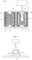
Figure 2 is exemplary of a possible act in embodiments, and -
Figure 3 essentially corresponds to a cross-sectional view along line III-III inFigure 2 reproduced in an enlarged scale. - In the ensuing description one or more specific details are illustrated, aimed at providing an in-depth understanding of examples of embodiments. The embodiments may be obtained without one or more of the specific details, or with other methods, components, materials, etc. In other cases, known structures, materials, or operations are not illustrated or described in detail so that certain aspects of embodiments will not be obscured.
- Reference to "an embodiment" or "one embodiment" in the framework of the present description is intended to indicate that a particular configuration, structure, or characteristic described in relation to the embodiment is comprised in at least one embodiment. Hence, phrases such as "in an embodiment" or "in one embodiment" that may be present in one or more points of the present description do not necessarily refer to one and the same embodiment. Moreover, particular conformations, structures, or characteristics may be combined in any adequate way in one or more embodiments.
- The references used herein are provided merely for convenience and hence do not define the extent of protection or the scope of the embodiments.
-
Figure 1 is a schematic representation of asemiconductor device 10 such as an integrated circuit observed in a plan (top) view. - As current in the art, together with other elements/features not visible in the figure, a
device 10 as exemplified herein may comprise a so-calledleadframe 12 having a (central, for instance)die pad area 14 and (at least) one semiconductor chip or die 16 attached onto thedie pad area 14 of theleadframe 12 via a soft-solder process. - "Soft solder" is a conventional designation in the art to designate solders such as, for instance, Tin-lead (Sn-Pb) solders, which are commercially available with tin concentrations between 5% and 70% by weight.
- A
package 18 can be molded onto the semiconductor die ordice 16 attached onto thedie pad area 14 of theleadframe 12 to provide a device package having the external (distal) tips of the leads in theleadframe 12 protruding from thepackage 18. - The general structure and manufacturing process of a
semiconductor device 10 as exemplified inFigure 1 (including the provision of various additional elements such as wire bonding coupling the leads of the leadframe to the semiconductor die or dice, and so on, not visible in the figure) are well known to those of skill in the art, which makes it unnecessary to provide a more detailed description herein. - A conventional solution for manufacturing a device such as the
semiconductor device 10 exemplified herein may involve providing aleadframe 12 in the form of (ribbon-like) strip of metal material such as copper. Such a strip may comprise plural sections indicated 12 inFigure 2 . Each of these includes a respectivedie pad area 14 onto which respective semiconductor dice can be attached. - The various sections of the ribbon-like structure can be eventually separated ("singulated") prior to or following molding of
respective packages 18 to provide individual devices. - A conventional solution in implementing a process as discussed previously involves forming onto the metal material (copper, for instance) of the leadframe 12 a so-called enhancing layer having higher affinity with the
molding compound 18 which is eventually molded onto theleadframe 12 and the semiconductor die ordice 16 attached thereon. - Such a molding compound may conventionally comprise resin material such as epoxy resin molding compound (EMC = Epoxy Molding Compound).
- As exemplified in
Figure 3 , providing the enhancing layer (over the portion of theleadframe 12 onto which the package compound is expected to be molded) may involve providing onto the basic material of the leadframe 12 (a metal such as copper, for instance) a coating (as exemplified at 20 inFigure 3 ) of another material (a metal such as silver, for instance) which is processed to form the enhancinglayer 22. - Materials such as silver being "precious" (and thus expensive) materials suggest that such a material is not applied a continuous layer/coating but rather applied spot-like in order to limit use of the (precious) metal plating to where effectively needed.
- The shaded areas indicated as 20 in
Figure 1 are exemplary of areas which may receive silver (Ag) applied spot-like thereon. - For instance, according to the treatment process designated NEAP 4.0 (NEAP = Non-Etching Adhesion Promoter) an upper layer (10-100nm) of silver oxide (AgOx) is formed "on top" of the
silver coating 20 as exemplified at 22. - As discussed previously, while promoting good adhesion with the package compound, the
enhancing layer 22 was found to adversely affect the attachment process of the semiconductor die or dice 16 onto thedie pad 14 of theleadframe 12. - Even without wishing to be bound to any specific theory in that respect, the enhancing
layer 22 may negatively affect "wettability" of the leadframe material (copper 12 coated by silver 20) by soft-solder attach material. - A composition of Pb 95%/Sn 5 % or sometimes 1-2% Ag and Sn balance may be exemplary of such a soft-solder attach material.
- As schematically represented in
Figures 2 and 3 , one or more embodiments may contemplate selectively removing theenhancing layer 22 at the region of thedie pad 14 onto which the semiconductor die ordice 16 is attached. - The wording "at" is intended to highlight the fact that selective removal of the
enhancing layer 22 does not necessarily have to involve the entirety of die pad area onto which the semiconductor die ordice 16 is attached. An increase of the area where (soft-solder) attach may take place without being adversely affected by the enhancing layer was however found to be beneficial. - Laser beam ablation (as indicated by L in
Figures 2 and 3 ) was found to be effective in performing such a selective removal of the enhancing layer with the capability of restoring the original wettability of the underlying leadframe material (for instance "pure"silver 20, as in the case exemplified inFigure 3 ). - Selective removal of the enhancing
layer 22 by laser beam ablation was found to result in "cleaning" the surface of the leadframe from which the enhancing layer is removed (for instance the surface of thesilver coating 20 inFigure 3 ) with an effect of that surface being melted and/or roughened. - As in common English usage, a surface being "roughened" indicates that such a surface is made rough.
- This was found to be beneficial in (further) promoting adhesion of the soft-solder material onto the leadframe and facilitating anchoring of the semiconductor die or dice 16 thereon, with reduced risk of delamination.
- Again, without wishing to be bound to any specific theory in that respect, such a surface melting/roughening may result in the contact surface of the soft-solder material to the leadframe being increased, thus giving rise to a synergistic increased wettability/increased contact surface resulting from (selective) removal of the enhancing layer.
- Experiments performed by the applicants show that laser beam radiation at a wavelength at about 1064 nm as produced by a YAG laser with specific power of 100 watt @ 1 mH (pulsed with pulse duration of 15 pSec) may provide firm soft-solder die attachment onto a silver-coated leadframe while an AgOx enhancing layer left in place onto the portions of the leadframe eventually contacted by the package molding compound facilitate satisfactory package delamination performance as desired.
- As exemplified herein, a method of manufacturing semiconductor devices (for instance, 10) may comprise:
- providing a leadframe (for instance, 12) having a die pad area (for instance, 14),
- attaching onto said die pad area at least one semiconductor die (for instance, 16) via soft-solder die attach material,
- forming a device package (for instance, 18) by molding package material onto the at least one semiconductor die attached onto said die pad area of the leadframe,
- providing onto said leadframe an enhancing layer (for instance, 22) countering device package delamination,
- removing (for instance, L) said enhancing layer from at least a portion of the die pad area, and
- attaching said at least one semiconductor die onto said die pad area via soft-solder die attach material provided where said enhancing layer has been removed.
- A method as exemplified herein may comprise removing said enhancing layer from said die pad area via laser beam ablation.
- In a method as exemplified herein, said enhancing layer may comprise processed silver, optionally Non-Etching Adhesion Promoter (NEAP)-processed.
- A method as exemplified herein may comprise:
- forming said leadframe of a first metal material,
- forming onto said leadframe a layer of a second metal material, and
- processing the surface of said second metal material opposite the first metal material to provide said enhancing layer.
- In a method as exemplified herein, said first metal material may comprises copper.
- In a method as exemplified herein, said second material may comprise silver.
- A semiconductor device (for instance, 10) as exemplified herein may comprise:
- a leadframe (for instance, 12) having a die pad area (for instance, 14),
- at least one semiconductor die (for instance, 16) attached onto said die pad area (14) via soft-solder die attach material,
- a device package (for instance, 18) of package material molded onto the at least one semiconductor die attached onto said die pad area of the leadframe, wherein:
- an enhancing layer (for instance, 22) is provided on said leadframe, the enhancing layer countering device package delamination, wherein said die pad area of the leadframe is at least partially exempt (for instance, L) from said enhancing layer, and
- the at least one semiconductor die is attached onto said die pad area via soft-solder die attach material provided where the die pad area of the leadframe is exempt from said enhancing layer.
- In a device as exemplified herein, where exempt from said enhancing layer, the die pad area of the leadframe may have a roughened surface wetted by said soft-solder die attach material.
- In a device as exemplified herein:
- said leadframe may comprise a first metal material, optionally copper, having formed thereon a layer of a second metal material, optionally silver, and
- said enhancing layer may comprise a processed (optionally Non-Etching Adhesion Promoter or NEAP)-processed layer of said second metal material.
- Without prejudice to the underlying principles, the details and embodiments may vary, even significantly, with respect to what has been described by way of example only without departing from the scope of protection.
- The extent of protection is defined by the annexed claims.
Claims (9)
- A method of manufacturing semiconductor devices (10), the method comprising:- providing a leadframe (12) having a die pad area (14),- attaching onto said die pad area (14) at least one semiconductor die (16) via soft-solder die attach material,- forming a device package (18) by molding package material onto the at least one semiconductor die (16) attached onto said die pad area (14) of the leadframe (12),wherein the method comprises:- providing onto said leadframe an enhancing layer (22) countering device package delamination,- removing (L) said enhancing layer from at least a portion of the die pad area (14), and- attaching said at least one semiconductor die (16) onto said die pad area (14) via soft-solder die attach material provided where said enhancing layer (22) has been removed.
- The method of claim 1, comprising removing said enhancing layer (22) from said die pad area (14) via laser beam ablation (L).
- The method of claim 1 or claim 2, wherein said enhancing layer (22) comprises processed silver (20).
- The method of any of the previous claims, comprising:- forming said leadframe (12) of a first metal material,- forming onto said leadframe (12) a layer of a second metal material (20), and- processing the surface of said second metal material (20) opposite the first metal material (12) to provide said enhancing layer (22).
- The method of claim 4, wherein said first metal material (12) comprises copper.
- The method of claim 4 or claim 5, wherein said second material (20, 22) comprises silver.
- A semiconductor device (10), comprising:- a leadframe (12) having a die pad area (14),- at least one semiconductor die (16) attached onto said die pad area (14) via soft-solder die attach material,- a device package (18) of package material molded onto the at least one semiconductor die (16) attached onto said die pad area (14) of the leadframe (12), wherein:- an enhancing layer (22) is provided on said leadframe (12), the enhancing layer (22) countering device package delamination, wherein said die pad area (14) of the leadframe (12) is at least partially exempt from said enhancing layer (22), and- the at least one semiconductor die is attached onto said die pad area via soft-solder die attach material provided where the die pad area (14) of the leadframe (12) is exempt from said enhancing layer (22).
- The device (10) of claim 7, in which, where exempt from said enhancing layer (22), the die pad area (14) of the leadframe has a roughened surface wetted by said soft-solder die attach material.
- The device (10) of claim 7 or claim 8, wherein:- said leadframe (12) comprises a first metal material, preferably copper, having formed thereon a layer of a second metal material (20), preferably silver, and- said enhancing layer (22) comprises a processed layer of said second metal material (20).
Applications Claiming Priority (1)
| Application Number | Priority Date | Filing Date | Title |
|---|---|---|---|
| IT102019000009501A IT201900009501A1 (en) | 2019-06-19 | 2019-06-19 | DIE ATTACHMENT PROCESS FOR SEMICONDUCTOR DEVICES AND CORRESPONDING SEMICONDUCTOR DEVICE |
Publications (2)
| Publication Number | Publication Date |
|---|---|
| EP3754703A1 true EP3754703A1 (en) | 2020-12-23 |
| EP3754703B1 EP3754703B1 (en) | 2022-08-03 |
Family
ID=68234200
Family Applications (1)
| Application Number | Title | Priority Date | Filing Date |
|---|---|---|---|
| EP20179296.7A Active EP3754703B1 (en) | 2019-06-19 | 2020-06-10 | A die attachment method for semiconductor devices and corresponding semiconductor device |
Country Status (4)
| Country | Link |
|---|---|
| US (1) | US11640931B2 (en) |
| EP (1) | EP3754703B1 (en) |
| CN (2) | CN112117199B (en) |
| IT (1) | IT201900009501A1 (en) |
Cited By (1)
| Publication number | Priority date | Publication date | Assignee | Title |
|---|---|---|---|---|
| IT202100031007A1 (en) * | 2021-12-10 | 2023-06-10 | St Microelectronics Srl | Method of attaching die into semiconductor devices and corresponding semiconductor device |
Families Citing this family (2)
| Publication number | Priority date | Publication date | Assignee | Title |
|---|---|---|---|---|
| IT201900009501A1 (en) * | 2019-06-19 | 2020-12-19 | St Microelectronics Srl | DIE ATTACHMENT PROCESS FOR SEMICONDUCTOR DEVICES AND CORRESPONDING SEMICONDUCTOR DEVICE |
| US20250273540A1 (en) | 2024-02-28 | 2025-08-28 | Stmicroelectronics International N.V. | Method of manufacturing semiconductor devices and corresponding semiconductor device |
Citations (5)
| Publication number | Priority date | Publication date | Assignee | Title |
|---|---|---|---|---|
| US7382059B2 (en) * | 2005-11-18 | 2008-06-03 | Semiconductor Components Industries, L.L.C. | Semiconductor package structure and method of manufacture |
| US20090250796A1 (en) * | 2008-04-04 | 2009-10-08 | Gem Services, Inc. | Semiconductor device package having features formed by stamping |
| JP5156658B2 (en) * | 2009-01-30 | 2013-03-06 | 株式会社日立製作所 | Electronic components for LSI |
| CN103594448A (en) * | 2013-11-15 | 2014-02-19 | 杰群电子科技(东莞)有限公司 | Lead frame |
| US9653385B1 (en) * | 2016-05-26 | 2017-05-16 | Sdi Corporation | Lead frame |
Family Cites Families (17)
| Publication number | Priority date | Publication date | Assignee | Title |
|---|---|---|---|---|
| KR100266726B1 (en) * | 1995-09-29 | 2000-09-15 | 기타지마 요시토시 | Leadframes and Semiconductor Devices with the Leadframes |
| US6943434B2 (en) | 2002-10-03 | 2005-09-13 | Fairchild Semiconductor Corporation | Method for maintaining solder thickness in flipchip attach packaging processes |
| US8993221B2 (en) * | 2012-02-10 | 2015-03-31 | Pixelligent Technologies, Llc | Block co-polymer photoresist |
| SG140574A1 (en) * | 2006-08-30 | 2008-03-28 | United Test & Assembly Ct Ltd | Method of producing a semiconductor package |
| JP5415106B2 (en) * | 2008-03-21 | 2014-02-12 | 住友化学株式会社 | Manufacturing method of resin package |
| DE102009008738A1 (en) * | 2009-02-12 | 2010-08-19 | Osram Opto Semiconductors Gmbh | Semiconductor device and method for manufacturing a semiconductor device |
| US20120153444A1 (en) * | 2009-06-18 | 2012-06-21 | Rohm Co., Ltd | Semiconductor device |
| WO2013018357A1 (en) * | 2011-08-01 | 2013-02-07 | 日本特殊陶業株式会社 | Semiconductor power module, method for manufacturing semiconductor power module, and circuit board |
| JP5975911B2 (en) * | 2013-03-15 | 2016-08-23 | ルネサスエレクトロニクス株式会社 | Semiconductor device |
| CN104576596B (en) * | 2013-10-25 | 2019-01-01 | 日月光半导体制造股份有限公司 | Semiconductor substrate and method for manufacturing the same |
| TWI610411B (en) | 2014-08-14 | 2018-01-01 | 艾馬克科技公司 | Laser assisted bonding for semiconductor die interconnect |
| US9941219B2 (en) * | 2014-09-19 | 2018-04-10 | Intel Corporation | Control of warpage using ABF GC cavity for embedded die package |
| JP7016677B2 (en) * | 2017-11-21 | 2022-02-07 | 新光電気工業株式会社 | Manufacturing method of lead frame, semiconductor device, lead frame |
| CN108436270B (en) * | 2018-03-26 | 2020-09-18 | 中国人民解放军陆军装甲兵学院 | Surface pretreatment method for aluminum alloy laser welding |
| US12564071B2 (en) * | 2019-02-27 | 2026-02-24 | Texas Instruments Incorporated | Laser ablation surface treatment for microelectronic assembly |
| IT201900009501A1 (en) * | 2019-06-19 | 2020-12-19 | St Microelectronics Srl | DIE ATTACHMENT PROCESS FOR SEMICONDUCTOR DEVICES AND CORRESPONDING SEMICONDUCTOR DEVICE |
| IT201900022641A1 (en) * | 2019-12-02 | 2021-06-02 | St Microelectronics Srl | PROCEDURE FOR MANUFACTURING SEMICONDUCTOR DEVICES, CORRESPONDING SEMICONDUCTOR DEVICE AND APPARATUS |
-
2019
- 2019-06-19 IT IT102019000009501A patent/IT201900009501A1/en unknown
-
2020
- 2020-06-10 EP EP20179296.7A patent/EP3754703B1/en active Active
- 2020-06-11 US US16/899,342 patent/US11640931B2/en active Active
- 2020-06-18 CN CN202010562192.0A patent/CN112117199B/en active Active
- 2020-06-18 CN CN202021138926.4U patent/CN212412003U/en active Active
Patent Citations (5)
| Publication number | Priority date | Publication date | Assignee | Title |
|---|---|---|---|---|
| US7382059B2 (en) * | 2005-11-18 | 2008-06-03 | Semiconductor Components Industries, L.L.C. | Semiconductor package structure and method of manufacture |
| US20090250796A1 (en) * | 2008-04-04 | 2009-10-08 | Gem Services, Inc. | Semiconductor device package having features formed by stamping |
| JP5156658B2 (en) * | 2009-01-30 | 2013-03-06 | 株式会社日立製作所 | Electronic components for LSI |
| CN103594448A (en) * | 2013-11-15 | 2014-02-19 | 杰群电子科技(东莞)有限公司 | Lead frame |
| US9653385B1 (en) * | 2016-05-26 | 2017-05-16 | Sdi Corporation | Lead frame |
Cited By (1)
| Publication number | Priority date | Publication date | Assignee | Title |
|---|---|---|---|---|
| IT202100031007A1 (en) * | 2021-12-10 | 2023-06-10 | St Microelectronics Srl | Method of attaching die into semiconductor devices and corresponding semiconductor device |
Also Published As
| Publication number | Publication date |
|---|---|
| US20200402895A1 (en) | 2020-12-24 |
| CN112117199A (en) | 2020-12-22 |
| CN212412003U (en) | 2021-01-26 |
| CN112117199B (en) | 2025-12-19 |
| EP3754703B1 (en) | 2022-08-03 |
| US11640931B2 (en) | 2023-05-02 |
| IT201900009501A1 (en) | 2020-12-19 |
Similar Documents
| Publication | Publication Date | Title |
|---|---|---|
| EP3754703B1 (en) | A die attachment method for semiconductor devices and corresponding semiconductor device | |
| US8435867B2 (en) | Method of manufacturing semiconductor device and method of manufacturing electronic device | |
| DE68905267T2 (en) | SEMICONDUCTOR ARRANGEMENT OF METAL BUMPER TYPE AND METHOD FOR THE PRODUCTION THEREOF. | |
| KR100720607B1 (en) | Semiconductor device | |
| WO2011123220A2 (en) | Packaging process to create wettable lead flank during board assembly | |
| US11594504B2 (en) | Nickel alloy for semiconductor packaging | |
| US20230187296A1 (en) | Die attachment method for semiconductor devices and corresponding semiconductor device | |
| US10937744B2 (en) | Semiconductor packages including roughening features | |
| US20170365575A1 (en) | Packaged IC With Solderable Sidewalls | |
| US10707154B2 (en) | Semiconductor device and method for manufacturing the same | |
| US12125803B2 (en) | Method of manufacturing semiconductor devices, corresponding apparatus and semiconductor device | |
| JP2017117840A (en) | Semiconductor device | |
| US7425503B1 (en) | Apparatus and method for enhanced thermal conductivity packages for high powered semiconductor devices | |
| JP2019096836A (en) | Semiconductor device and method for manufacturing the same | |
| CN114078716B (en) | Semiconductor devices and their manufacturing methods | |
| JP2003249616A (en) | Electronic component lead cutting method | |
| US20070087587A1 (en) | Method for manufacturing circuit board for semiconductor package | |
| JPH09148509A (en) | Lead frame for semiconductor device and surface treatment method thereof | |
| JPS63187654A (en) | Lead frame for electronic component | |
| US20250149410A1 (en) | Semiconductor device and method of manufacturing the same | |
| CN121666102A (en) | Semiconductor packages with wettable side wings and related methods | |
| JPS6363622B2 (en) | ||
| JPH0445978B2 (en) | ||
| JPS61139055A (en) | Semiconductor device | |
| JP2000061684A (en) | Bonding material in place of Pb and mounted electronic parts plated with alloy for mounting bonding with the bonding material |
Legal Events
| Date | Code | Title | Description |
|---|---|---|---|
| PUAI | Public reference made under article 153(3) epc to a published international application that has entered the european phase |
Free format text: ORIGINAL CODE: 0009012 |
|
| STAA | Information on the status of an ep patent application or granted ep patent |
Free format text: STATUS: THE APPLICATION HAS BEEN PUBLISHED |
|
| AK | Designated contracting states |
Kind code of ref document: A1 Designated state(s): AL AT BE BG CH CY CZ DE DK EE ES FI FR GB GR HR HU IE IS IT LI LT LU LV MC MK MT NL NO PL PT RO RS SE SI SK SM TR |
|
| AX | Request for extension of the european patent |
Extension state: BA ME |
|
| STAA | Information on the status of an ep patent application or granted ep patent |
Free format text: STATUS: REQUEST FOR EXAMINATION WAS MADE |
|
| 17P | Request for examination filed |
Effective date: 20210603 |
|
| RBV | Designated contracting states (corrected) |
Designated state(s): AL AT BE BG CH CY CZ DE DK EE ES FI FR GB GR HR HU IE IS IT LI LT LU LV MC MK MT NL NO PL PT RO RS SE SI SK SM TR |
|
| GRAP | Despatch of communication of intention to grant a patent |
Free format text: ORIGINAL CODE: EPIDOSNIGR1 |
|
| STAA | Information on the status of an ep patent application or granted ep patent |
Free format text: STATUS: GRANT OF PATENT IS INTENDED |
|
| INTG | Intention to grant announced |
Effective date: 20220324 |
|
| GRAS | Grant fee paid |
Free format text: ORIGINAL CODE: EPIDOSNIGR3 |
|
| GRAA | (expected) grant |
Free format text: ORIGINAL CODE: 0009210 |
|
| STAA | Information on the status of an ep patent application or granted ep patent |
Free format text: STATUS: THE PATENT HAS BEEN GRANTED |
|
| AK | Designated contracting states |
Kind code of ref document: B1 Designated state(s): AL AT BE BG CH CY CZ DE DK EE ES FI FR GB GR HR HU IE IS IT LI LT LU LV MC MK MT NL NO PL PT RO RS SE SI SK SM TR |
|
| REG | Reference to a national code |
Ref country code: AT Ref legal event code: REF Ref document number: 1509442 Country of ref document: AT Kind code of ref document: T Effective date: 20220815 Ref country code: CH Ref legal event code: EP |
|
| REG | Reference to a national code |
Ref country code: DE Ref legal event code: R096 Ref document number: 602020004301 Country of ref document: DE |
|
| REG | Reference to a national code |
Ref country code: IE Ref legal event code: FG4D |
|
| REG | Reference to a national code |
Ref country code: LT Ref legal event code: MG9D |
|
| REG | Reference to a national code |
Ref country code: NL Ref legal event code: MP Effective date: 20220803 |
|
| PG25 | Lapsed in a contracting state [announced via postgrant information from national office to epo] |
Ref country code: SE Free format text: LAPSE BECAUSE OF FAILURE TO SUBMIT A TRANSLATION OF THE DESCRIPTION OR TO PAY THE FEE WITHIN THE PRESCRIBED TIME-LIMIT Effective date: 20220803 Ref country code: RS Free format text: LAPSE BECAUSE OF FAILURE TO SUBMIT A TRANSLATION OF THE DESCRIPTION OR TO PAY THE FEE WITHIN THE PRESCRIBED TIME-LIMIT Effective date: 20220803 Ref country code: PT Free format text: LAPSE BECAUSE OF FAILURE TO SUBMIT A TRANSLATION OF THE DESCRIPTION OR TO PAY THE FEE WITHIN THE PRESCRIBED TIME-LIMIT Effective date: 20221205 Ref country code: NO Free format text: LAPSE BECAUSE OF FAILURE TO SUBMIT A TRANSLATION OF THE DESCRIPTION OR TO PAY THE FEE WITHIN THE PRESCRIBED TIME-LIMIT Effective date: 20221103 Ref country code: NL Free format text: LAPSE BECAUSE OF FAILURE TO SUBMIT A TRANSLATION OF THE DESCRIPTION OR TO PAY THE FEE WITHIN THE PRESCRIBED TIME-LIMIT Effective date: 20220803 Ref country code: LV Free format text: LAPSE BECAUSE OF FAILURE TO SUBMIT A TRANSLATION OF THE DESCRIPTION OR TO PAY THE FEE WITHIN THE PRESCRIBED TIME-LIMIT Effective date: 20220803 Ref country code: LT Free format text: LAPSE BECAUSE OF FAILURE TO SUBMIT A TRANSLATION OF THE DESCRIPTION OR TO PAY THE FEE WITHIN THE PRESCRIBED TIME-LIMIT Effective date: 20220803 Ref country code: FI Free format text: LAPSE BECAUSE OF FAILURE TO SUBMIT A TRANSLATION OF THE DESCRIPTION OR TO PAY THE FEE WITHIN THE PRESCRIBED TIME-LIMIT Effective date: 20220803 Ref country code: ES Free format text: LAPSE BECAUSE OF FAILURE TO SUBMIT A TRANSLATION OF THE DESCRIPTION OR TO PAY THE FEE WITHIN THE PRESCRIBED TIME-LIMIT Effective date: 20220803 |
|
| REG | Reference to a national code |
Ref country code: AT Ref legal event code: MK05 Ref document number: 1509442 Country of ref document: AT Kind code of ref document: T Effective date: 20220803 |
|
| PG25 | Lapsed in a contracting state [announced via postgrant information from national office to epo] |
Ref country code: PL Free format text: LAPSE BECAUSE OF FAILURE TO SUBMIT A TRANSLATION OF THE DESCRIPTION OR TO PAY THE FEE WITHIN THE PRESCRIBED TIME-LIMIT Effective date: 20220803 Ref country code: IS Free format text: LAPSE BECAUSE OF FAILURE TO SUBMIT A TRANSLATION OF THE DESCRIPTION OR TO PAY THE FEE WITHIN THE PRESCRIBED TIME-LIMIT Effective date: 20221203 Ref country code: HR Free format text: LAPSE BECAUSE OF FAILURE TO SUBMIT A TRANSLATION OF THE DESCRIPTION OR TO PAY THE FEE WITHIN THE PRESCRIBED TIME-LIMIT Effective date: 20220803 Ref country code: GR Free format text: LAPSE BECAUSE OF FAILURE TO SUBMIT A TRANSLATION OF THE DESCRIPTION OR TO PAY THE FEE WITHIN THE PRESCRIBED TIME-LIMIT Effective date: 20221104 |
|
| PG25 | Lapsed in a contracting state [announced via postgrant information from national office to epo] |
Ref country code: SM Free format text: LAPSE BECAUSE OF FAILURE TO SUBMIT A TRANSLATION OF THE DESCRIPTION OR TO PAY THE FEE WITHIN THE PRESCRIBED TIME-LIMIT Effective date: 20220803 Ref country code: RO Free format text: LAPSE BECAUSE OF FAILURE TO SUBMIT A TRANSLATION OF THE DESCRIPTION OR TO PAY THE FEE WITHIN THE PRESCRIBED TIME-LIMIT Effective date: 20220803 Ref country code: DK Free format text: LAPSE BECAUSE OF FAILURE TO SUBMIT A TRANSLATION OF THE DESCRIPTION OR TO PAY THE FEE WITHIN THE PRESCRIBED TIME-LIMIT Effective date: 20220803 Ref country code: CZ Free format text: LAPSE BECAUSE OF FAILURE TO SUBMIT A TRANSLATION OF THE DESCRIPTION OR TO PAY THE FEE WITHIN THE PRESCRIBED TIME-LIMIT Effective date: 20220803 Ref country code: AT Free format text: LAPSE BECAUSE OF FAILURE TO SUBMIT A TRANSLATION OF THE DESCRIPTION OR TO PAY THE FEE WITHIN THE PRESCRIBED TIME-LIMIT Effective date: 20220803 |
|
| REG | Reference to a national code |
Ref country code: DE Ref legal event code: R097 Ref document number: 602020004301 Country of ref document: DE |
|
| PG25 | Lapsed in a contracting state [announced via postgrant information from national office to epo] |
Ref country code: SK Free format text: LAPSE BECAUSE OF FAILURE TO SUBMIT A TRANSLATION OF THE DESCRIPTION OR TO PAY THE FEE WITHIN THE PRESCRIBED TIME-LIMIT Effective date: 20220803 Ref country code: EE Free format text: LAPSE BECAUSE OF FAILURE TO SUBMIT A TRANSLATION OF THE DESCRIPTION OR TO PAY THE FEE WITHIN THE PRESCRIBED TIME-LIMIT Effective date: 20220803 |
|
| PLBE | No opposition filed within time limit |
Free format text: ORIGINAL CODE: 0009261 |
|
| STAA | Information on the status of an ep patent application or granted ep patent |
Free format text: STATUS: NO OPPOSITION FILED WITHIN TIME LIMIT |
|
| PG25 | Lapsed in a contracting state [announced via postgrant information from national office to epo] |
Ref country code: AL Free format text: LAPSE BECAUSE OF FAILURE TO SUBMIT A TRANSLATION OF THE DESCRIPTION OR TO PAY THE FEE WITHIN THE PRESCRIBED TIME-LIMIT Effective date: 20220803 |
|
| 26N | No opposition filed |
Effective date: 20230504 |
|
| PG25 | Lapsed in a contracting state [announced via postgrant information from national office to epo] |
Ref country code: SI Free format text: LAPSE BECAUSE OF FAILURE TO SUBMIT A TRANSLATION OF THE DESCRIPTION OR TO PAY THE FEE WITHIN THE PRESCRIBED TIME-LIMIT Effective date: 20220803 |
|
| PG25 | Lapsed in a contracting state [announced via postgrant information from national office to epo] |
Ref country code: MC Free format text: LAPSE BECAUSE OF FAILURE TO SUBMIT A TRANSLATION OF THE DESCRIPTION OR TO PAY THE FEE WITHIN THE PRESCRIBED TIME-LIMIT Effective date: 20220803 |
|
| PG25 | Lapsed in a contracting state [announced via postgrant information from national office to epo] |
Ref country code: MC Free format text: LAPSE BECAUSE OF FAILURE TO SUBMIT A TRANSLATION OF THE DESCRIPTION OR TO PAY THE FEE WITHIN THE PRESCRIBED TIME-LIMIT Effective date: 20220803 |
|
| REG | Reference to a national code |
Ref country code: CH Ref legal event code: PL |
|
| REG | Reference to a national code |
Ref country code: BE Ref legal event code: MM Effective date: 20230630 |
|
| PG25 | Lapsed in a contracting state [announced via postgrant information from national office to epo] |
Ref country code: LU Free format text: LAPSE BECAUSE OF NON-PAYMENT OF DUE FEES Effective date: 20230610 |
|
| REG | Reference to a national code |
Ref country code: IE Ref legal event code: MM4A |
|
| PG25 | Lapsed in a contracting state [announced via postgrant information from national office to epo] |
Ref country code: LU Free format text: LAPSE BECAUSE OF NON-PAYMENT OF DUE FEES Effective date: 20230610 |
|
| PG25 | Lapsed in a contracting state [announced via postgrant information from national office to epo] |
Ref country code: IE Free format text: LAPSE BECAUSE OF NON-PAYMENT OF DUE FEES Effective date: 20230610 |
|
| PG25 | Lapsed in a contracting state [announced via postgrant information from national office to epo] |
Ref country code: IE Free format text: LAPSE BECAUSE OF NON-PAYMENT OF DUE FEES Effective date: 20230610 Ref country code: CH Free format text: LAPSE BECAUSE OF NON-PAYMENT OF DUE FEES Effective date: 20230630 |
|
| PG25 | Lapsed in a contracting state [announced via postgrant information from national office to epo] |
Ref country code: IT Free format text: LAPSE BECAUSE OF FAILURE TO SUBMIT A TRANSLATION OF THE DESCRIPTION OR TO PAY THE FEE WITHIN THE PRESCRIBED TIME-LIMIT Effective date: 20220803 Ref country code: FR Free format text: LAPSE BECAUSE OF NON-PAYMENT OF DUE FEES Effective date: 20230630 Ref country code: BE Free format text: LAPSE BECAUSE OF NON-PAYMENT OF DUE FEES Effective date: 20230630 |
|
| PG25 | Lapsed in a contracting state [announced via postgrant information from national office to epo] |
Ref country code: BG Free format text: LAPSE BECAUSE OF FAILURE TO SUBMIT A TRANSLATION OF THE DESCRIPTION OR TO PAY THE FEE WITHIN THE PRESCRIBED TIME-LIMIT Effective date: 20220803 |
|
| PG25 | Lapsed in a contracting state [announced via postgrant information from national office to epo] |
Ref country code: BG Free format text: LAPSE BECAUSE OF FAILURE TO SUBMIT A TRANSLATION OF THE DESCRIPTION OR TO PAY THE FEE WITHIN THE PRESCRIBED TIME-LIMIT Effective date: 20220803 |
|
| GBPC | Gb: european patent ceased through non-payment of renewal fee |
Effective date: 20240610 |
|
| PG25 | Lapsed in a contracting state [announced via postgrant information from national office to epo] |
Ref country code: GB Free format text: LAPSE BECAUSE OF NON-PAYMENT OF DUE FEES Effective date: 20240610 |
|
| PGFP | Annual fee paid to national office [announced via postgrant information from national office to epo] |
Ref country code: DE Payment date: 20250520 Year of fee payment: 6 |
|
| PG25 | Lapsed in a contracting state [announced via postgrant information from national office to epo] |
Ref country code: CY Free format text: LAPSE BECAUSE OF FAILURE TO SUBMIT A TRANSLATION OF THE DESCRIPTION OR TO PAY THE FEE WITHIN THE PRESCRIBED TIME-LIMIT; INVALID AB INITIO Effective date: 20200610 |
|
| PG25 | Lapsed in a contracting state [announced via postgrant information from national office to epo] |
Ref country code: HU Free format text: LAPSE BECAUSE OF FAILURE TO SUBMIT A TRANSLATION OF THE DESCRIPTION OR TO PAY THE FEE WITHIN THE PRESCRIBED TIME-LIMIT; INVALID AB INITIO Effective date: 20200610 |
|
| REG | Reference to a national code |
Ref country code: DE Ref legal event code: R079 Ref document number: 602020004301 Country of ref document: DE Free format text: PREVIOUS MAIN CLASS: H01L0023495000 Ipc: H10W0070400000 |
|
| PG25 | Lapsed in a contracting state [announced via postgrant information from national office to epo] |
Ref country code: TR Free format text: LAPSE BECAUSE OF FAILURE TO SUBMIT A TRANSLATION OF THE DESCRIPTION OR TO PAY THE FEE WITHIN THE PRESCRIBED TIME-LIMIT Effective date: 20220803 |